ksz8863mll/fll/rll - integrated 3-port 10/100...
TRANSCRIPT

KSZ8863MLL/FLL/RLLIntegrated 3-Port 10/100 Managed Switch
with PHYs
Features
• Advanced Switch Features- IEEE 802.1q VLAN Support for Up to 16 Groups
(Full Range of VLAN IDs)- VLAN ID Tag/Untag Options, Per Port Basis- IEEE 802.1p/q Tag Insertion or Removal on a
Per Port Basis (Egress)- Programmable Rate Limiting at the Ingress and
Egress on a Per Port Basis- Broadcast Storm Protection with Percent Con-
trol (Global and Per Port Basis)- IEEE 802.1d Rapid Spanning Tree Protocol
Support- Tail Tag Mode (1 byte Added before FCS) Sup-
port at Port 3 to Inform the Processor which Ingress Port Receives the Packet and its Prior-ity
- Bypass Feature that Automatically Sustains the Switch Function between Port 1 and Port 2 when CPU (Port 3 Interface) Goes to the Sleep Mode
- Self-Address Filtering- Individual MAC Address for Port 1 and Port 2- Supports RMII Interface and 50 MHz Reference
Clock Output- IGMP Snooping (IPv4) Support for Multicast
Packet Filtering- IPv4/IPv6 QoS Support- MAC Filtering Function to Forward Unknown
Unicast Packets to Specified Port• Comprehensive Configuration Register Access
- Serial Management Interface (SMI) to All Inter-nal Registers
- MII Management (MIIM) Interface to PHY Reg-isters
- High Speed SPI and I2C Interface to All Internal Registers
- I/O Pins Strapping and EEPROM to Program Selective Registers in Unmanaged Switch Mode
- Control Registers Configurable on the Fly (Port-Priority, 802.1p/d/q, AN…)
• QoS/CoS Packet Prioritization Support- Per Port, 802.1p and DiffServ-Based- Re-Mapping of 802.1p Priority Field Per Port
basis, Four Priority Levels• Proven Integrated 3-Port 10/100 Ethernet Switch
- 3rd Generation Switch with Three MACs and Two PHYs Fully Compliant with IEEE 802.3u Standard
- Non-Blocking Switch Fabric Ensures Fast Packet Delivery by Utilizing a 1k MAC Address Lookup Table and a Store-and-Forward Archi-tecture
- Full-Duplex IEEE 802.3x Flow Control (PAUSE) with Force Mode Option
- Half-Duplex Back Pressure Flow Control- HP Auto MDI-X for Reliable Detection of and
Correction for Straight-Through and Crossover Cables with Disable and Enable Option
- LinkMD® TDR-Based Cable Diagnostics Permit Identification of Faulty Copper Cabling
- MII Interface Supports Both MAC Mode and PHY Mode
- Comprehensive LED Indicator Support for Link, Activity, Full-/Half-Duplex and 10/100 Speed
- HBM ESD Rating 4 kV• Switch Monitoring Features
- Port Mirroring/Monitoring/Sniffing: Ingress and/or Egress Traffic to Any Port or MII
- MIB Counters for Fully Compliant Statistics Gathering 34 MIB Counters Per Port
- Loopback Modes for Remote Diagnostic of Fail-ure
• Low Power Dissipation- Full-Chip Software Power-Down (Register Con-
figuration Not Saved) - Energy-Detect Mode Support- Dynamic Clock Tree Shutdown Feature- Per Port Based Software Power-Save on PHY
(Idle Link Detection, Register Configuration Pre-served)
- Voltages: Single 3.3V Supply with Internal 1.8V LDO for 3.3V VDDIO
- Optional 3.3V, 2.5V, and 1.8V for VDDIO- Transceiver Power 3.3V for VDDA_3.3
• Industrial Temperature Range: –40°C to +85°C• Available in a 48-Pin LQFP, Lead-Free Package
Applications
• VoIP Phone• Set-Top/Game Box• Automotive• Industrial Control• IPTV POF• SOHO Residential Gateway• Broadband Gateway/Firewall/VPN• Integrated DSL/Cable Modem• Wireless LAN Access Point + Gateway• Standalone 10/100 Switch
2017 Microchip Technology Inc. DS00002335B-page 1

KSZ8863MLL/FLL/RLL
TO OUR VALUED CUSTOMERS
It is our intention to provide our valued customers with the best documentation possible to ensure successful use of your Microchipproducts. To this end, we will continue to improve our publications to better suit your needs. Our publications will be refined andenhanced as new volumes and updates are introduced.
If you have any questions or comments regarding this publication, please contact the Marketing Communications Department viaE-mail at [email protected]. We welcome your feedback.
Most Current Data SheetTo obtain the most up-to-date version of this data sheet, please register at our Worldwide Web site at:
http://www.microchip.com
You can determine the version of a data sheet by examining its literature number found on the bottom outside corner of any page. The last character of the literature number is the version number, (e.g., DS30000000A is version A of document DS30000000).
ErrataAn errata sheet, describing minor operational differences from the data sheet and recommended workarounds, may exist for cur-rent devices. As device/documentation issues become known to us, we will publish an errata sheet. The errata will specify therevision of silicon and revision of document to which it applies.
To determine if an errata sheet exists for a particular device, please check with one of the following:• Microchip’s Worldwide Web site; http://www.microchip.com• Your local Microchip sales office (see last page)
When contacting a sales office, please specify which device, revision of silicon and data sheet (include -literature number) you areusing.
Customer Notification SystemRegister on our web site at www.microchip.com to receive the most current information on all of our products.
DS00002335B-page 2 2017 Microchip Technology Inc.

2017 Microchip Technology Inc. DS00002335B-page 3
KSZ8863MLL/FLL/RLL
Table of Contents
1.0 Introduction ..................................................................................................................................................................................... 42.0 Pin Description and Configuration .................................................................................................................................................. 53.0 Functional Description .................................................................................................................................................................. 114.0 Register Descriptions .................................................................................................................................................................... 365.0 Operational Characteristics ........................................................................................................................................................... 716.0 Electrical Characteristics ............................................................................................................................................................... 727.0 Timing Specifications .................................................................................................................................................................... 748.0 Reset Circuit ................................................................................................................................................................................. 849.0 Selection of Isolation Transformers .............................................................................................................................................. 8510.0 Package Outline .......................................................................................................................................................................... 86Appendix A: Data Sheet Revision History ........................................................................................................................................... 87The Microchip Web Site ...................................................................................................................................................................... 88Customer Change Notification Service ............................................................................................................................................... 88Customer Support ............................................................................................................................................................................... 88Product Identification System ............................................................................................................................................................. 89

KSZ8863MLL/FLL/RLL
DS00002335B-page 4 2017 Microchip Technology Inc.
1.0 INTRODUCTION
1.1 General Description
KSZ8863MLL, KSZ8863FLL, and KSZ8863RLL are highly integrated 3-port switch-on-a-chip ICs in the industry’s small-est footprint. They are designed to enable a new generation of low port count, cost-sensitive, and power-efficient 10/100 Mbps switch systems. Low power consumption, advanced power management, and sophisticated QoS features(for example, IPv6 priority classification support) make these devices ideal for IPTV, IP-STB, VoIP, automotive, andindustrial applications.
The KSZ8863 family is designed to support the GREEN requirement in today’s switch systems. Advanced power man-agement schemes include software power down, per port power down, and energy detect mode that shuts down thetransceiver when a port is idle.
KSZ8863MLL/FLL/RLL also offers a bypass mode that enables system-level power saving. In this mode, the processorconnected to the switch through the MII interface can be shut down without impacting the normal switch operation.
The configurations provided by the KSZ8863 family enable the flexibility to meet the requirements of different applica-tions:
• KSZ8863MLL: Two 10/100BASE-T/TX transceivers and one MII interface
• KSZ8863RLL: Two 10/100BASE-T/TX transceivers and one RMII interface
• KSZ8863FLL: One 100BASE-FX, one 10/100BASE-T/TX transceivers, and one MII interface
The devices are available in RoHS-compliant 48-pin LQFP packages. Industrial-grade and automotive-grade are alsoavailable.
FIGURE 1-1: SYSTEM BLOCK DIAGRAM
1K LOOK-UPENGINE
QUEUEMANAGEMENT
BUFFERMANAGEMENT
FRAMEBUFFERS
MIBCOUNTERS
EEPROMINTERFACE
YTI
ROI
RP ,
GNI
GGA
T NA
LV ,
LO
RTN
OC
WOL
F ,OF
IF
10/100MAC 1
10/100MAC 2
10/100MAC 3
10/100T/TX/FXPHY 1
10/100T/TX
PHY 2
HP AUTOMDIX
HP AUTOMDIX
2x MII/RMII
SPISPI
CONTROLREGISTERS
MIIM
SMI
STRAP INCONFIGURATION
LEDDRIVERS
I2C
P1 LED[1:0]
P2 LED[1:0]

KSZ8863MLL/FLL/RLL
2.0 PIN DESCRIPTION AND CONFIGURATION
FIGURE 2-1: 48-PIN 7 MM X 7 MM LQFP ASSIGNMENT, (TOP VIEW)
SM
TXD
33/E
N_R
EFC
LKO
_3S
MTX
EN
3X
2X1
NC
SM
TXD
32S
MTX
D31
SM
TXD
30
RXM1RXP1TXM1TXP1
VDDA_3.3ISET
VDDA_1.8RXM2
13 14 15 16 17 18 19 20
12345678
48-pinLQFP
RXP2AGNDTXM2TXP2
9101112
GN
DV
DD
IOS
MTX
C3/
RE
FCLK
I_3
SM
TXE
R3/
MII_
LIN
K_3
21 22 23 24
SCL_MDCINTRNSCRS3SCOL3VDDCGNDSMRXC3SMRXD30
3635343332313029
SMRXD31SMRXD32SMRXD33/REFCLKO_3SMRXDV3
28272625
P1L
ED
0P
2LE
D1
P2L
ED
0R
STN
FXS
D1
P1L
ED
1V
DD
CO
GN
D
48 47 46 45 44 43 42 41
VD
DIO
SP
ISN
SP
IQS
DA
_MD
IO
40 39 38 37
2017 Microchip Technology Inc. DS00002335B-page 5
KSZ8863MLL/FLL/RLL
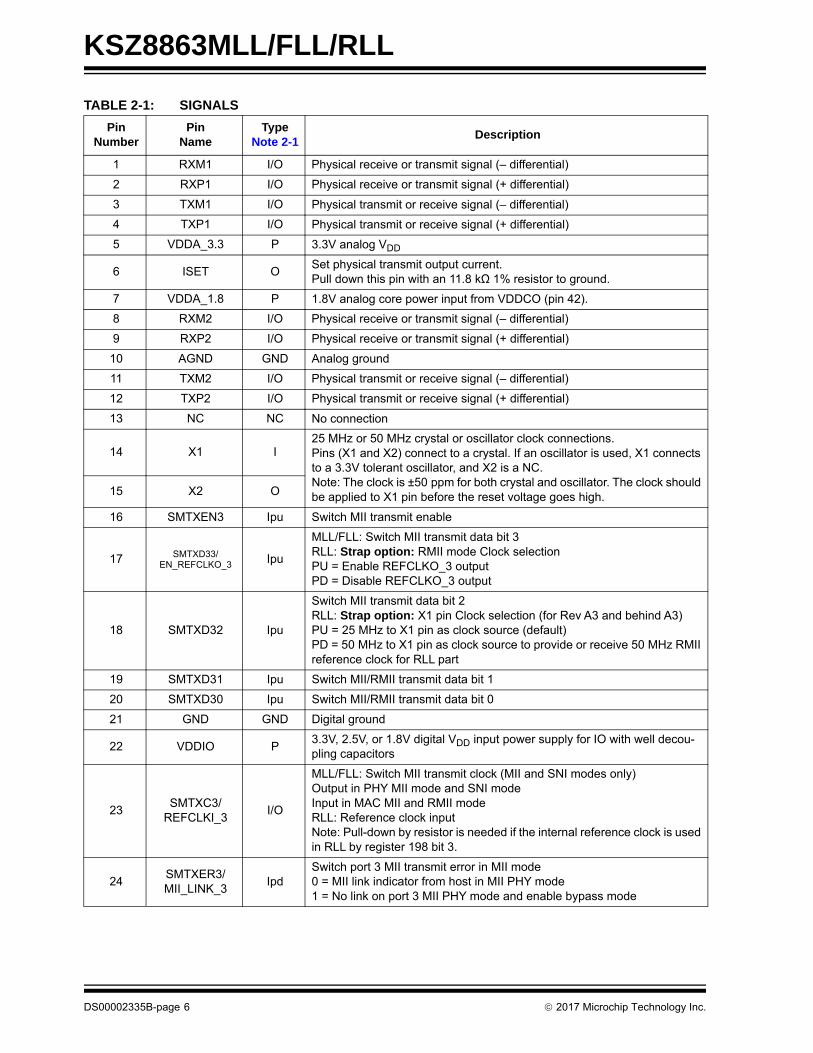
TABLE 2-1: SIGNALS
Pin Number
PinName
TypeNote 2-1
Description
1 RXM1 I/O Physical receive or transmit signal (– differential)
2 RXP1 I/O Physical receive or transmit signal (+ differential)
3 TXM1 I/O Physical transmit or receive signal (– differential)
4 TXP1 I/O Physical transmit or receive signal (+ differential)
5 VDDA_3.3 P 3.3V analog VDD
6 ISET OSet physical transmit output current.Pull down this pin with an 11.8 kΩ 1% resistor to ground.
7 VDDA_1.8 P 1.8V analog core power input from VDDCO (pin 42).
8 RXM2 I/O Physical receive or transmit signal (– differential)
9 RXP2 I/O Physical receive or transmit signal (+ differential)
10 AGND GND Analog ground
11 TXM2 I/O Physical transmit or receive signal (– differential)
12 TXP2 I/O Physical transmit or receive signal (+ differential)
13 NC NC No connection
14 X1 I25 MHz or 50 MHz crystal or oscillator clock connections.Pins (X1 and X2) connect to a crystal. If an oscillator is used, X1 connects to a 3.3V tolerant oscillator, and X2 is a NC.Note: The clock is ±50 ppm for both crystal and oscillator. The clock should be applied to X1 pin before the reset voltage goes high.15 X2 O
16 SMTXEN3 Ipu Switch MII transmit enable
17 SMTXD33/EN_REFCLKO_3 Ipu
MLL/FLL: Switch MII transmit data bit 3RLL: Strap option: RMII mode Clock selection PU = Enable REFCLKO_3 output PD = Disable REFCLKO_3 output
18 SMTXD32 Ipu
Switch MII transmit data bit 2RLL: Strap option: X1 pin Clock selection (for Rev A3 and behind A3)PU = 25 MHz to X1 pin as clock source (default)PD = 50 MHz to X1 pin as clock source to provide or receive 50 MHz RMII reference clock for RLL part
19 SMTXD31 Ipu Switch MII/RMII transmit data bit 1
20 SMTXD30 Ipu Switch MII/RMII transmit data bit 0
21 GND GND Digital ground
22 VDDIO P3.3V, 2.5V, or 1.8V digital VDD input power supply for IO with well decou-pling capacitors
23SMTXC3/
REFCLKI_3I/O
MLL/FLL: Switch MII transmit clock (MII and SNI modes only)Output in PHY MII mode and SNI modeInput in MAC MII and RMII modeRLL: Reference clock inputNote: Pull-down by resistor is needed if the internal reference clock is used in RLL by register 198 bit 3.
24SMTXER3/MII_LINK_3
IpdSwitch port 3 MII transmit error in MII mode0 = MII link indicator from host in MII PHY mode1 = No link on port 3 MII PHY mode and enable bypass mode
DS00002335B-page 6 2017 Microchip Technology Inc.

KSZ8863MLL/FLL/RLL
25 SMRXDV3 Ipu/O
Switch MII/RMII receive data validStrap option: Force duplex mode (P1DPX)PU = Port 1 default to full-duplex mode if P1ANEN = 1 and auto-negotia-tion fails. Force port 1 in full-duplex mode if P1ANEN = 0.PD = Port 1 default to half-duplex mode if P1ANEN = 1 and auto-negotia-tion fails. Force port 1 in half-duplex mode if P1ANEN = 0.
26SMRXD33/
REFCLKO_3Ipu/O
MLL/FLL: Switch MII receive data bit 3RLL: Output reference clock in RMII mode.Strap option: enable auto-negotiation on port 2 (P2ANEN)PU = EnablePD = Disable
27 SMRXD32 Ipu/O
Switch MII receive data bit 2Strap option: Force the speed on port 2 (P2SPD)PU = Force port 2 to 100BT if P2ANEN = 0PD = Force port 2 to 10BT if P2ANEN = 0
28 SMRXD31 Ipu/O
Switch MII/RMII receive data bit 1Strap option: Force duplex mode (P2DPX)PU = Port 2 default to full-duplex mode if P2ANEN = 1 and auto-negotia-tion fails. Force port 2 in full-duplex mode if P2ANEN = 0.PD = Port 2 set to half-duplex mode if P2ANEN = 1 and auto-negotiation fails. Force port 2 in half-duplex mode if P2ANEN = 0.
29 SMRXD30 Ipu/O
Switch MII/RMII receive data bit 0Strap option: Force flow control on port 2 (P2FFC)PU = Always enable (force) port 2 flow control feature.PD = Port 2 flow control feature enable is determined by auto-negotiation result.
30 SMRXC3 I/OSwitch MII receive clock.Output in PHY MII modeInput in MAC MII mode
31 GND GND Digital ground
32 VDDC P 1.8V digital core power input from VDDCO (pin 42)
33 SCOL3 Ipu/O Switch MII collision detect
34 SCRS3 Ipu/O Switch MII carrier sense
35 INTRN OpuInterruptActive-low signal to host CPU to indicate an interrupt status bit is set when lost link. Refer to register 187 and 188.
36 SCL_MDC I/OSPI Slave mode/I2C Slave mode: clock inputI2C Master mode: clock outputMIIM clock input
37 SDA_MDIO Ipu/O
SPI Slave mode: serial data inputI2C Master/Slave mode: serial data input/outputMIIM: Data input/outputNote: An external pull-up is needed on this pin when it is in use.
38 SPIQ Ipd/O
SPI Slave mode: serial data outputNote: An external pull-up is needed on this pin when it is in use.Strap option: Force flow control on port 1 (P1FFC)PU = Always enable (force) port 1 flow control featurePD = Port 1 flow control feature enable is determined by auto-negotiation result.
TABLE 2-1: SIGNALS (CONTINUED)
Pin Number
PinName
TypeNote 2-1
Description
2017 Microchip Technology Inc. DS00002335B-page 7

KSZ8863MLL/FLL/RLL
39 SPISN Ipd
SPI Slave mode: chip select (active-low)When SPISN is high, KSZ8863MLL/FLL/RLL is deselected and SPIQ is held in a high impedance state.A high-to-low transition is used to initiate SPI data transfer.Note: An external pull-up is needed on this pin when using SPI or MDC/MDIO-MIIM/SMI mode.
40 VDDIO P3.3V, 2.5V, or 1.8V digital VDD input power supply for IO with well decou-pling capacitors
41 GND GND Digital ground
42 VDDCO P
1.8V core power voltage output (internal 1.8V LDO regulator output)This 1.8V output pin provides power to both VDDA_1.8 and VDDC input pins. Note: Internally, 1.8V LDO regulator input comes from VDDIO. Do not con-nect an external power supply to VDDCO pin. The ferrite bead is requested between analog and digital 1.8V core power.
43 P1LED1 Ipu/O
Port 1 LED Indicators:Default: Speed (refer to register 195 bit [5:4])Strap option: Force the speed on port 1 (P1SPD)PU = Force port 1 to 100BT if P1ANEN = 0PD = Force port 1 to 10BT if P1ANEN = 0
44 P1LED0 Ipd/O
Port 1 LED Indicators:Default: Link/Act. (refer to register 195 bit [5:4])Strap option: Enable auto-negotiation on port 1 (P1ANEN)PU = Enable (better to pull up in design)PD = Disable (default)
TABLE 2-1: SIGNALS (CONTINUED)
Pin Number
PinName
TypeNote 2-1
Description
DS00002335B-page 8 2017 Microchip Technology Inc.

KSZ8863MLL/FLL/RLL
45 P2LED1 Ipu/O
Port 2 LED Indicators:Default: Speed (refer to register 195 bit [5:4])Strap option: Serial bus configuration
Port 2 LED Indicators:Default: Link/Act. (refer to register 195 bit [5:4])Strap option: Serial bus configurationSerial bus configuration pins to select mode of access to KSZ8863MLL/FLL/RLL internal registers.
[P2LED1, P2LED0] = [0, 0] — I2C Master (EEPROM) mode(If EEPROM is not detected, the KSZ8863MLL/FLL/RLL is configured with the default values of its internal registers and the values of its strap-in pins.)
[P2LED1, P2LED0] = [0, 1] — I2C Slave modeThe external I2C Master drives the SCL_MDC clock. The KSZ8863MLL/FLL/RLL device addresses are:1011_1111 <read>1011_1110 <write>
[P2LED1, P2LED0] = [1, 0] — SPI Slave mode
[P2LED1, P2LED0] = [1, 1] – SMI/MIIM modeIn SMI mode, KSZ8863MLL/FLL/RLL provides access to all its internal 8-bit registers through its SCL_MDC and SDA_MDIO pins.In MIIM mode, KSZ8863MLL/FLL/RLL provides access to its 16-bit MIIM registers through its SDC_MDC and SDA_MDIO pins.
46 P2LED0 Ipu/O
47 RSTN Ipu Hardware reset pin (active-low)
48 FXSD1 IMLL/RLL: No connection or connect to analog ground by 1 kΩ pull-down resistor.FLL: Fiber signal detect
TABLE 2-1: SIGNALS (CONTINUED)
Pin Number
PinName
TypeNote 2-1
Description
Interface Signals Type Description
SPIQ O Not used (tri-stated)
SCL_MDC O I2C clock
SDA_MDIO I/O I2C data I/O
SPISN I Not used
Interface Signals Type Description
SPIQ O Not used (tri-stated)
SCL_MDC I I2C clock
SDA_MDIO I/O I2C data I/O
SPISN I Not used
Interface Signals Type Description
SPIQ O SPI data out
SCL_MDC I SPI clock
SDA_MDIO I SPI data in
SPISN I SPI chip select
2017 Microchip Technology Inc. DS00002335B-page 9

KSZ8863MLL/FLL/RLL
Note 2-1 P = power supplyGND = GroundI = InputO = OutputI/O = Bi-directionalIpu/O = Input with internal pull-up during reset; output pin otherwise.Ipu = Input with internal pull-up.Ipd = Input with internal pull-down.Opu = Output with internal pull-up.Opd = Output with internal pull-down.Speed: Low (100BASE-TX), High (10BASE-T)Full-Duplex: Low (full-duplex), High (half-duplex)Activity: Toggle (transmit/receive activity)Link: Low (link), High (no link)
DS00002335B-page 10 2017 Microchip Technology Inc.

KSZ8863MLL/FLL/RLL
3.0 FUNCTIONAL DESCRIPTION
KSZ8863MLL/FLL/RLL contains two 10/100 physical layer transceivers and three MAC units with an integrated layer 2managed switch.
KSZ8863MLL/FLL/RLL has the flexibility to reside in either a managed or unmanaged design. In a managed design, thehost processor has complete control of KSZ8863MLL/FLL/RLL via the SMI interface, MIIM interface, SPI bus, or I2Cbus. An unmanaged design is achieved through I/O strapping and/or EEPROM programming at system reset time.
On the media side, KSZ8863MLL/FLL/RLL supports IEEE 802.3 10BASE-T and 100BASE-TX on both PHY ports. Phys-ical signal transmission and reception are enhanced through the use of patented analog circuitries that make the designmore efficient and allow for lower power consumption and smaller chip die size.
3.1 Physical Layer Transceiver
3.1.1 100BASE-TX TRANSMIT
The 100BASE-TX transmit function performs parallel-to-serial conversion, 4B/5B coding, scrambling, NRZ-to-NRZI con-version, and MLT3 encoding and transmission.
The circuitry starts with a parallel-to-serial conversion, which converts the MII data from the MAC into a 125 MHz serialbit stream. The data and control stream is then converted into 4B/5B coding, followed by a scrambler. The serializeddata is further converted from NRZ-to-NRZI format, and then transmitted in MLT3 current output. The output current isset by an external 1% 11.8 kΩ resistor for the 1:1 transformer ratio.
The output signal has a typical rise/fall time of 4 ns and complies with the ANSI TP-PMD standard regarding amplitudebalance, overshoot, and timing jitter. The wave-shaped 10BASE-T output is also incorporated into the 100BASE-TXtransmitter.
3.1.2 100BASE-TX RECEIVE
The 100BASE-TX receiver function performs adaptive equalization, DC restoration, MLT3-to-NRZI conversion, data andclock recovery, NRZI-to-NRZ conversion, de-scrambling, 4B/5B decoding, and serial-to-parallel conversion.
The receiving side starts with the equalization filter to compensate for inter-symbol interference (ISI) over the twistedpair cable. Since the amplitude loss and phase distortion is a function of the cable length, the equalizer must adjust itscharacteristics to optimize performance. In this design, the variable equalizer makes an initial estimation based on com-parisons of incoming signal strength against some known cable characteristics, and then tunes itself for optimization.This is an ongoing process and self-adjusts against environmental changes such as temperature variations.
Next, the equalized signal goes through a DC restoration and data conversion block. The DC restoration circuit is usedto compensate for the effect of baseline wander and to improve the dynamic range. The differential data conversioncircuit converts the MLT3 format back to NRZI. The slicing threshold is also adaptive.
The clock recovery circuit extracts the 125 MHz clock from the edges of the NRZI signal. This recovered clock is thenused to convert the NRZI signal into the NRZ format. This signal is sent through the de-scrambler followed by the 4B/5B decoder. Finally, the NRZ serial data is converted to the MII format and provided as the input data to the MAC.
3.1.3 PLL CLOCK SYNTHESIZER
KSZ8863MLL/FLL/RLL generates 125 MHz, 62.5 MHz, and 31.25 MHz clocks for system timing. Internal clocks aregenerated from an external 25 MHz or 50 MHz crystal or oscillator. KSZ8863RLL can generate a 50 MHz referenceclock for the RMII interface.
3.1.4 SCRAMBLER/DE-SCRAMBLER (100BASE-TX ONLY)
The purpose of the scrambler is to spread the power spectrum of the signal to reduce electromagnetic interference (EMI)and baseline wander. Transmitted data is scrambled through the use of an 11-bit wide linear feedback shift register(LFSR). The scrambler generates a 2047-bit non-repetitive sequence, and the receiver then de-scrambles the incomingdata stream using the same sequence as at the transmitter.
3.1.5 100BASE-FX OPERATION
The 100BASE-FX operation is similar to the 100BASE-TX operation with the differences being that the scrambler/de-scrambler and MLT3 encoder/decoder are bypassed on transmission and reception. In addition, auto-negotiation isbypassed and auto MDI/MDI-X is disabled.
2017 Microchip Technology Inc. DS00002335B-page 11

KSZ8863MLL/FLL/RLL
3.1.6 100BASE-FX SIGNAL DETECTION
In 100BASE-FX operation, FXSD (fiber signal detect), input pin 48, is usually connected to the fiber transceiver SD (sig-nal detect) output pin. The fiber signal threshold can be selected by register 192 bit 6 for port 1. When FXSD is less thanthe threshold, no fiber signal is detected and a far-end fault (FEF) is generated. When FXSD is over the threshold, thefiber signal is detected.
Alternatively, the designer may choose not to implement the FEF feature. In this case, the FXSD input pin is tied highto force 100BASE-FX mode.
100BASE-FX signal detection is summarized in Table 3-1:
To ensure proper operation, a resistive voltage divider is recommended to adjust the fiber transceiver SD output voltageswing to match the FXSD pin’s input voltage threshold.
3.1.7 100BASE-FX FAR-END FAULT
A far-end fault (FEF) occurs when the signal detection is logically false on the receive side of the fiber transceiver. TheKSZ8863FLL detects a FEF when its FXSD input is below the Fiber Signal Threshold. When a FEF is detected,KSZ8863FLL signals its fiber link partner that a FEF has occurred by sending 84 1’s followed by a zero in the idle periodbetween frames. By default, FEF is enabled.
3.1.8 10BASE-T TRANSMIT
The 10BASE-T driver is incorporated with the 100BASE-TX driver to allow for transmission using the same magnetics.They are internally wave-shaped and pre-emphasized into outputs with a typical 2.3V amplitude. The harmonic contentsare at least 27 dB below the fundamental frequency when driven by an all-ones Manchester-encoded signal.
3.1.9 10BASE-T RECEIVE
On the receive side, input buffers and level detecting squelch circuits are employed. A differential input receiver circuitand a phase-locked loop (PLL) perform the decoding function. The Manchester-encoded data stream is separated intoclock signal and NRZ data. A squelch circuit rejects signals with levels less than 400 mV or with short pulse widths toprevent noise at the RXP-or-RXM input from falsely triggering the decoder. When the input exceeds the squelch limit,the PLL locks onto the incoming signal and KSZ8863MLL/FLL/RLL decodes a data frame. The receiver clock is main-tained active during idle periods in between data reception.
3.1.10 MDI/MDI-X AUTO CROSSOVER
To eliminate the need for crossover cables between similar devices, KSZ8863MLL/FLL/RLL supports HP Auto MDI/MDI-X and IEEE 802.3u standard MDI/MDI-X auto crossover. HP Auto MDI/MDI-X is the default.
The auto-sense function detects remote transmit and receive pairs and correctly assigns transmit and receive pairs forthe KSZ8863MLL/FLL/RLL device. This feature is extremely useful when end users are unaware of cable types, andalso, saves on an additional uplink configuration connection. The auto-crossover feature can be disabled through theport control registers, or MIIM PHY registers.
The IEEE 802.3u standard MDI and MDI-X definitions are illustrated in Table 3-2.
TABLE 3-1: FX SIGNAL THRESHOLD
Register 192 Bit 7, Bit 6 (Port 1) Fiber Signal Threshold at FXSD
1 2.0V
0 1.2V
TABLE 3-2: MDI/MDI-X PIN DEFINITIONS
MDI MDI-X
RJ-45 Pins Signals RJ-45 Pins Signals
1 TD+ 1 RD+
2 TD– 2 RD–
3 RD+ 3 TD+
6 RD– 6 TD–
DS00002335B-page 12 2017 Microchip Technology Inc.

KSZ8863MLL/FLL/RLL
3.1.10.1 Straight Cable
A straight cable connects an MDI device to an MDI-X device, or an MDI-X device to an MDI device. Figure 3-1 depictsa typical straight cable connection between a NIC card (MDI) and a switch, or hub (MDI-X).
FIGURE 3-1: TYPICAL STRAIGHT CABLE CONNECTION
Receive PairTransmit Pair
Receive Pair
1
2
3
4
5
6
7
8
1
2
3
4
5
6
7
8
Transmit Pair
Modular Connector(RJ-45)
NIC
StraightCable
10/100 EthernetMedia Dependent Interface
10/100 EthernetMedia Dependent Interface
Modular Connector(RJ-45)
HUB(Repeater or Switch)
2017 Microchip Technology Inc. DS00002335B-page 13

KSZ8863MLL/FLL/RLL
3.1.10.2 Crossover Cable
A crossover cable connects an MDI device to another MDI device, or an MDI-X device to another MDI-X device.Figure 3-2 shows a typical crossover cable connection between two switches or hubs (two MDI-X devices).
3.1.11 AUTO-NEGOTIATION
KSZ8863MLL/FLL/RLL conforms to the auto-negotiation protocol defined in Clause 28 of the IEEE 802.3u specification.
Auto-negotiation allows unshielded twisted pair (UTP) link partners to select the best common mode of operation. Inauto-negotiation, link partners advertise their capabilities across the link to each other. If auto-negotiation is not sup-ported or the KSZ8863MLL/FLL/RLL link partner is forced to bypass auto-negotiation, KSZ8863MLL/FLL/RLL sets itsoperating mode by observing the signal at its receiver. This is known as parallel detection, and allows KSZ8863MLL/FLL/RLL to establish a link by listening for a fixed signal protocol in the absence of auto-negotiation advertisement pro-tocol.
The link up process is shown in Figure 3-3.
FIGURE 3-2: TYPICAL CROSSOVER CABLE CONNECTION
Receive Pair Receive Pair
Transmit Pair
1
2
3
4
5
6
7
8
1
2
3
4
5
6
7
8
Transmit Pair
10/100 EthernetMedia Dependent Interface
10/100 EthernetMedia Dependent Interface
Modular Connector (RJ-45)HUB
(Repeater or Switch)
Modular Connector (RJ-45)HUB
(Repeater or Switch)
CrossoverCable
DS00002335B-page 14 2017 Microchip Technology Inc.

KSZ8863MLL/FLL/RLL
FIGURE 3-3: AUTO-NEGOTIATION AND PARALLEL OPERATION
3.1.12 LINKMD® CABLE DIAGNOSTICS
KSZ8863MLL/FLL/RLL supports LinkMD. The LinkMD feature utilizes time domain reflectometry (TDR) to analyze thecabling plant for common cabling problems such as open circuits, short circuits, and impedance mismatches.
LinkMD works by sending a pulse of known amplitude and duration down the MDI and MDI-X pairs and then analyzesthe shape of the reflected signal. Timing the pulse duration gives an indication of the distance to the cabling fault. Inter-nal circuitry displays the TDR information in a user-readable digital format.
Cable diagnostics are only valid for copper connections and do not support fiber optic operation.
3.1.12.1 Access
LinkMD is initiated through accessing the PHY special control/status registers 26, 42 and the LinkMD result registers27, 43 for ports 1 and 2 respectively; and in conjunction with the port registers control 13 for ports 1 and 2 respectivelyto disable Auto MDI/MDIX.
Alternatively, the MIIM PHY registers 0 and 29 can be used for LinkMD access.
3.1.12.2 Usage
The following is a sample procedure for using LinkMD with registers 42, 43, 45 on port 2:
1. Disable auto MDI/MDI-X by writing a ‘1’ to register 45, bit [2] to enable manual control over the differential pairused to transmit the LinkMD pulse.
START AUTO-NEGOTIATION
FORCE LINK SETTING
LISTEN FOR 10BASE-T LINK PULSES
LISTEN FOR 100BASE-TXIDLES
ATTEMPT AUTO-NEGOTIATION
LINK MODE SET
BYPASS AUTO-NEGOTIATIONAND SET LINK MODE
LINK MODE SET?
PARALLELOPERATIONNO
YES
YES
NO
JOIN FLOW
2017 Microchip Technology Inc. DS00002335B-page 15
KSZ8863MLL/FLL/RLL
2. Start cable diagnostic test by writing a ‘1’ to register 42, bit [4]. This enable bit is self-clearing.
3. Wait (poll) for register 42, bit [4] to return a ‘0’, indicating cable diagnostic test is complete.
4. Read cable diagnostic test results in register 42, bits [6:5]. The results are as follows:
00 = normal condition (valid test)
01 = open condition detected in cable (valid test)
10 = short condition detected in cable (valid test)
11 = cable diagnostic test failed (invalid test)
The ‘11’ case, invalid test, occurs when KSZ8863MLL/FLL/RLL is unable to shut down the link partner. In this instance,the test is not run because it is impossible for KSZ8863MLL/FLL/RLL to determine if the detected signal is a reflectionof the signal generated or a signal from another source.
5. Get the distance to fault by concatenating register 42, bit [0] and register 43, bits [7:0]; and multiplying the resultby a constant of 0.4. The distance to the cable fault can be determined by the following formula:
EQUATION 3-1:
Concatenated values of registers 42 and 43 are converted to decimal before multiplying by 0.4.
The constant (0.4) may be calibrated for different cabling conditions, including cables with a velocity of propagation thatvaries significantly from the norm.
3.2 Power Management
KSZ8863MLL/FLL/RLL supports enhanced power management feature in low power state with energy detection toensure low-power dissipation during device idle periods. There are five operation modes under the power managementfunction, which is controlled by two bits in register 195 (0xC3) and one bit in register 29 (0x1D), 45(0x2D) as shownbelow:
• Register 195 bit [1:0] = 00 Normal Operation Mode
• Register 195 bit [1:0] = 01 Energy Detect Mode
• Register 195 bit [1:0] = 10 Soft Power Down Mode
• Register 195 bit [1:0] = 11 Power Saving Mode
• Register 29, 45 bit 3 = 1 Port Based Power Down Mode
Table 3-3 indicates all internal function blocks status under four different power management operation modes.
3.2.1 NORMAL OPERATION MODE
This is the default setting bit [1:0] = 00 in register 195 after the chip power-up or hardware reset. When KSZ8863MLL/FLL/RLL is in this normal operation mode, all PLL clocks are running, PHY and MAC are on, and the host interface isready for CPU read or write.
TABLE 3-3: INTERNAL FUNCTION BLOCK STATUS
KSZ8863MLL/FLL/RLL Function Blocks
Power Management Operation Modes
Normal ModePower Saving
ModeEnergy Detect
ModeSoft Power Down
Mode
Internal PLL Clock Enabled Enabled Disabled Disabled
Tx/Rx PHY EnabledRx unused block
disabledEnergy detect at Rx Disabled
MAC Enabled Enabled Disabled Disabled
Host Interface Enabled Enabled Disabled Disabled
D Dis cetan·
to cable fault in meters 0.4 Register 26 bit [0] Register 27 bits [7:0] =
DS00002335B-page 16 2017 Microchip Technology Inc.

KSZ8863MLL/FLL/RLL
During the normal operation mode, the host CPU can set the bit [1:0] in register 195 to transit the current normal oper-ation mode to any one of the other three power management operation modes.
3.2.2 POWER SAVING MODE
The power saving mode is entered when auto-negotiation mode is enabled, cable is disconnected, and bit [1:0] = 11 inregister 195 is set. When KSZ8863MLL/FLL/RLL is in this mode, all PLL clocks are enabled, MAC is on, all internal reg-ister values are not changed, and the host interface is ready for CPU read or write. In this mode, it mainly controls thePHY transceiver on or off based on line status to achieve power saving. The PHY remains transmitting and only turnsoff the unused receiver block. Once the activity resumes due to plugging a cable or attempting by the far end to establisha link, KSZ8863MLL/FLL/RLL can automatically enable the PHY power-up to normal power state from power savingmode.
During the power saving mode, the host CPU can set bit [1:0] = 0 in register 195 to transit the current power savingmode to any one of the other three power management operation modes.
3.2.3 ENERGY DETECT MODE
The energy detect mode provides a mechanism to save more power than in the normal operation mode whenKSZ8863MLL/FLL/RLL is not connected to an active link partner. In this mode, the device saves up to 87% of the power.If the cable is not plugged, KSZ8863MLL/FLL/RLL can automatically enter a low-power state, that is, the energy detectmode. In this mode, KSZ8863MLL/FLL/RLL keeps transmitting 120 ns width pulses at a rate of 1 pulse/second. Oncethe activity resumes due to plugging a cable or attempting by the far end to establish a link, KSZ8863MLL/FLL/RLL canautomatically power up to normal power state in energy detect mode.
Energy detect mode consists of two states: normal power state and low power state. In low power state, KSZ8863MLL/FLL/RLL reduces the power consumption by disabling all circuitries except the energy detect circuitry of the receiver.The energy detect mode is entered by setting bit [1:0] = 01 in register 195. When KSZ8863MLL/FLL/RLL is in this mode,it monitors the cable energy. If there is no energy on the cable for a time longer than the pre-configured value at bit [7:0]Go-Sleep time in register 196, KSZ8863MLL/FLL/RLL goes into a low power state. When KSZ8863MLL/FLL/RLL is inlow power state, it keeps monitoring the cable energy. Once the energy is detected from the cable, KSZ8863MLL/FLL/RLL enters the normal power state. When KSZ8863MLL/FLL/RLL is in the normal power state, it can transmit or receivepacket from the cable.
It saves about 87% of the power when the MII interface is in PHY mode (register 53 bit 7 = 0), pin SMTXER3/MII_LINK_3is connected to High, register 195 bit [1:0] = 01, bit 2 = 1(Disable PLL), and no cables are connected.
3.2.4 SOFT POWER DOWN MODE
The soft power down mode is entered by setting bit [1:0] = 10 in register 195. When KSZ8863MLL/FLL/RLL is in thismode, all PLL clocks are disabled, PHY and MAC are off, and all internal register values are not changed. When thehost set bit [1:0] = 00 in register 195, this device reverts from current soft power down mode to normal operation mode.
3.2.5 PORT-BASED POWER DOWN MODE
In addition, KSZ8863MLL/FLL/RLL features a per-port power down mode. To save power, a PHY port that is not in usecan be powered down via the port control register 29 or 45 bit 3, or the MIIM PHY register. It saves about 15 mA per port.
3.3 MAC and Switch
3.3.1 ADDRESS LOOKUP
The internal lookup table stores MAC addresses and their associated information. It contains a 1K unicast address tableplus switching information.
KSZ8863MLL/FLL/RLL is guaranteed to learn 1K addresses and distinguishes itself from hash-based lookup tables,which depending on the operating environment and probabilities, may not guarantee the absolute number of addressesit can learn.
3.3.2 LEARNING
The internal lookup engine updates its table with a new entry if the following conditions are met:
• The received packet's Source Address (SA) does not exist in the lookup table.
• The received packet is good; the packet has no receiving errors and is of legal length.
2017 Microchip Technology Inc. DS00002335B-page 17
KSZ8863MLL/FLL/RLL
The lookup engine inserts the qualified SA into the table, along with the port number and time stamp. If the table is full,the last entry of the table is deleted to make room for the new entry.
3.3.3 MIGRATION
The internal lookup engine also monitors whether a station has moved. If a station has moved, it updates the tableaccordingly. Migration happens when the following conditions are met:
• The received packet’s SA is in the table, but the associated source port information is different.
• The received packet is good; the packet has no receiving errors and is of legal length.
The lookup engine updates the existing record in the table with the new source port information.
3.3.4 AGING
The lookup engine updates the time stamp information of a record whenever the corresponding SA appears. The timestamp is used in the aging process. If a record is not updated for a period of time, the lookup engine removes the recordfrom the table. The lookup engine constantly performs the aging process and continuously removes aging records. Theaging period is about 200 seconds. This feature can be enabled or disabled through register 3 (0x03) bit [2].
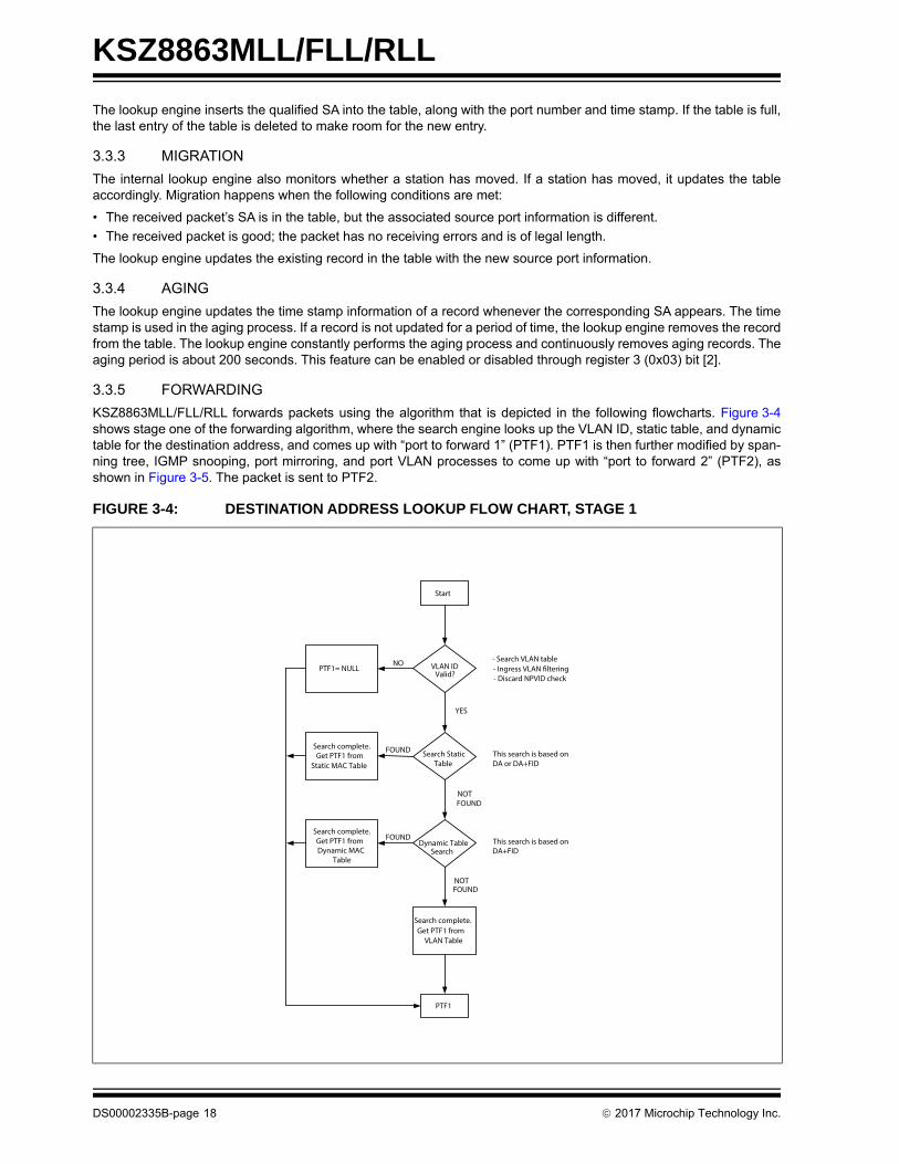
3.3.5 FORWARDING
KSZ8863MLL/FLL/RLL forwards packets using the algorithm that is depicted in the following flowcharts. Figure 3-4shows stage one of the forwarding algorithm, where the search engine looks up the VLAN ID, static table, and dynamictable for the destination address, and comes up with “port to forward 1” (PTF1). PTF1 is then further modified by span-ning tree, IGMP snooping, port mirroring, and port VLAN processes to come up with “port to forward 2” (PTF2), asshown in Figure 3-5. The packet is sent to PTF2.
FIGURE 3-4: DESTINATION ADDRESS LOOKUP FLOW CHART, STAGE 1
Start
VLAN IDValid?
PTF1= NULL
Search StaticTable
Search complete.Get PTF1 from
Static MAC Table
Dynamic TableSearch
Search complete.Get PTF1 from
VLAN Table
Search complete.Get PTF1 fromDynamic MAC
Table
PTF1
- Search VLAN table- Ingress VLAN filtering- Discard NPVID check
YES
NO
FOUND
NOTFOUND
FOUND
NOTFOUND
This search is based onDA or DA+FID
This search is based onDA+FID
DS00002335B-page 18 2017 Microchip Technology Inc.

KSZ8863MLL/FLL/RLL
KSZ8863MLL/FLL/RLL does not forward the following packets:
1. Error packets: These include framing errors, Frame Check Sequence (FCS) errors, alignment errors, and illegalsize packet errors.
2. IEEE802.3x PAUSE frames: KSZ8863MLL/FLL/RLL intercepts these packets and performs full duplex flow con-trol accordingly.
3. “Local” packets: Based on destination address (DA) lookup. If the destination port from the lookup table matchesthe port from which the packet originated, the packet is defined as local.
3.3.6 SWITCHING ENGINE
KSZ8863MLL/FLL/RLL features a high-performance switching engine to move data to and from the MAC’s packet buf-fers. It operates in store and forward mode, while the efficient switching mechanism reduces overall latency.
The switching engine has a 32-kb internal frame buffer. This buffer pool is shared among all three ports. There are atotal of 256 buffers available. Each buffer is sized at 128 bytes.
3.3.7 MAC OPERATION
KSZ8863MLL/FLL/RLL strictly abides by IEEE 802.3 standards to maximize compatibility.
3.3.7.1 Inter Packet Gap (IPG)
If a frame is successfully transmitted, the 96 bits time IPG is measured between the two consecutive MTXEN. If thecurrent packet is experiencing collision, the 96 bits time IPG is measured from MCRS and the next MTXEN.
3.3.7.2 Back-Off Algorithm
KSZ8863MLL/FLL/RLL implements the IEEE 802.3 standard for the binary exponential back-off algorithm and theoptional “aggressive mode” back-off. After 16 collisions, the packet is optionally dropped depending on the switch con-figuration for register 4 (0x04) bit [3].
FIGURE 3-5: DESTINATION ADDRESS RESOLUTION FLOW CHART, STAGE 2
Spanning TreeProcess
PTF1
IGMP Process
Port MirrorProcess
Port VLANMembership
Check
PTF2
- Check receiving port's receive enable bit- Check destination port's transmit enable bit- Check whether packets are special (BPDU or specified)
- RX Mirror- TX Mirror- RX or TX Mirror- RX and TX Mirror
- Applied to MAC #1 and MAC #2- MAC #3 is reserved for microprocessor- IGMP will be forwarded to port 3
2017 Microchip Technology Inc. DS00002335B-page 19

KSZ8863MLL/FLL/RLL
3.3.7.3 Late Collision
If a transmit packet experiences collisions after 512 bit times of the transmission, the packet is dropped.
3.3.7.4 Illegal Frames
KSZ8863MLL/FLL/RLL discards frames less than 64 bytes and can be programmed to accept frames up to 1518 bytes,1536 bytes, or 1916 bytes. These maximum frame size settings are programmed in register 4 (0x04). SinceKSZ8863MLL/FLL/RLL supports VLAN tags, the maximum sizing is adjusted when these tags are present.
3.3.7.5 Full-Duplex Flow Control
KSZ8863MLL/FLL/RLL supports the standard IEEE 802.3x flow control frames on both transmit and receive sides.
On the receive side, if KSZ8863MLL/FLL/RLL receives a pause control frame, KSZ8863MLL/FLL/RLL does not transmitthe next normal frame until the timer, specified in the pause control frame, expires. If another pause frame is receivedbefore the current timer expires, the timer is updated with the new value in the second pause frame. During this period(while it is flow controlled), only flow control packets from KSZ8863MLL/FLL/RLL are transmitted.
On the transmit side, KSZ8863MLL/FLL/RLL has intelligent and efficient ways to determine when to invoke flow control.The flow control is based on availability of the system resources, including available buffers, available transmit queuesand available receive queues.
KSZ8863MLL/FLL/RLL will flow control a port that has just received a packet if the destination port resource is busy.KSZ8863MLL/FLL/RLL issues a flow control frame (XOFF) containing the maximum pause time defined by the IEEE802.3x standard. Once the resource is freed up, KSZ8863MLL/FLL/RLL sends out the other flow control frame (XON)with zero pause time to turn off the flow control (turn on transmission to the port). A hysteresis feature is provided toprevent the flow control mechanism from being constantly activated and deactivated.
KSZ8863MLL/FLL/RLL flow controls all ports if the receive queue becomes full.
3.3.7.6 Half-Duplex Backpressure
A half-duplex backpressure option (not in IEEE 802.3 standards) is also provided. The activation and deactivation con-ditions are the same as a full-duplex flow control. If backpressure is required, KSZ8863MLL/FLL/RLL sends preamblesto defer the other stations' transmission (carrier sense deference).
To avoid jabber and excessive deference (as defined in the IEEE 802.3 standard), after a certain time, KSZ8863MLL/FLL/RLL discontinues the carrier sense and then raises it again quickly. This short silent time (no carrier sense) preventsother stations from sending out packets, thus keeping other stations in a carrier sense deferred state. If the port haspackets to send during a backpressure situation, the carrier sense type backpressure is interrupted and those packetsare transmitted instead. If there are no additional packets to send, carrier sense type backpressure is activated againuntil switch resources free up. If a collision occurs, the binary exponential back-off algorithm is skipped and carrier senseis generated immediately, thus reducing the chance of further collisions and maintaining carrier sense to prevent packetreception.
To ensure that no packet is lost in 10BASE-T or 100BASE-TX half-duplex modes, the user must enable the following:
• Aggressive back-off (register 3 (0x03), bit [0])
• No excessive collision drop (register 4 (0x04), bit [3])
Note that these bits are not set as defaults because it is not the IEEE standard.
3.3.7.7 Broadcast Storm Protection
KSZ8863MLL/FLL/RLL has an intelligent option to protect the switch system from receiving too many broadcast pack-ets. As the broadcast packets are forwarded to all ports except the source port, an excessive number of switchresources (bandwidth and available space in transmit queues) may be utilized. KSZ8863MLL/FLL/RLL can opt toinclude “multicast packets” for storm control. The broadcast storm rate parameters are programmed globally and canbe enabled or disabled on a per-port basis. The rate is based on a 67 ms interval for 100BT and a 500 ms interval for10BT. At the beginning of each interval, the counter is cleared to zero, and the rate limit mechanism starts to count thenumber of bytes during the interval. The rate definition is described in register 6 (0x06) and 7 (0x07). The default settingis 0x63 (99 decimal). This is equal to a rate of 1%, calculated as follows:
148,800 frames/sec × 67 ms/interval × 1% = 99 frames/interval (approx.) = 0x63
Note: The 148,800 frames/sec is based on 64-byte block of packets in 100BASE-TX with 12 bytes of IPG and 8 bytesof preamble between two packets.
DS00002335B-page 20 2017 Microchip Technology Inc.

KSZ8863MLL/FLL/RLL
3.3.7.8 Port Individual MAC Address and Source Port Filtering
KSZ8863MLL/FLL/RLL provides individual MAC address for port 1 and port 2. They can be set at registers 142-147 and148-153. The packet is filtered if its source address matches the MAC address of port 1 or port 2 when register 21 and37 bit 6 is set to 1, respectively. For example, the packet is dropped after it completes the loop of a ring network.
3.3.8 MII INTERFACE OPERATION
The Media Independent Interface (MII) is specified in Clause 22 of the IEEE 802.3u standard. It provides a commoninterface between physical layer and MAC layer devices. The MII provided by KSZ8863MLL/FLL is connected to thedevice’s third MAC; the MII default is PHY mode and can be set to MAC mode with the register 53 bit 7. The interfacecontains two distinct groups of signals: one for transmission and the other for reception. Table 3-4 describes the signalsused by the MII bus.
The MII operates in either PHY mode or MAC mode. The data interface is nibble-wide and runs at ¼ the network bit rate(not encoded). Additional signals on the transmit side indicate when data is valid or when an error occurs during trans-mission. Similarly, the receive side has signals that convey when the data is valid and without physical layer errors. Forhalf-duplex operation, the SCOL signal indicates if a collision has occurred during transmission.
KSZ8863MLL/FLL does not provide the MRXER signal for PHY mode operation, and the MTXER signal for MAC modeoperation. Normally, MRXER indicates a receive error coming from the physical layer device and MTXER indicates atransmit error from the MAC device. Because the switch filters error frames, these MII error signals are not used byKSZ8863MLL/FLL. So, for PHY mode operation, if the device interfacing with KSZ8863MLL/FLL has an MRXER inputpin, it needs to be tied low. And, for MAC mode operation, if the device interfacing with KSZ8863MLL/FLL has anMTXER input pin, it also needs to be tied low.
KSZ8863MLL/FLL provides a bypass feature in the MII PHY mode. Pin SMTXER3/MII_LINK is used for MII link status.If the host is powered down, pin MII_LINK goes to high. In this case, no new ingress frames from port 1 or port 2 aresent out through port 3, and the frames for port 3 already in packet memory are flushed out.
3.3.9 RMII INTERFACE OPERATION
The Reduced Media Independent Interface (RMII) specifies a low pin count Media Independent Interface (MII). RMIIprovides a common interface between physical layer and MAC layer devices, and has the following key characteristics:
• Ports 10 Mbps and 100 Mbps data rates
• Uses a single 50 MHz clock reference (provided internally or externally)
TABLE 3-4: MII SIGNALS
PHY Mode Connections
Pin Description
MAC Mode Connections
External MACController Signals
KSZ8863MLL/FLLPHY Signals
External PHY Signals
KSZ8863MLL/FLLMAC Signals
MTXEN SMTXEN3 Transmit Enable MTXEN SMRXDV3
MTXER SMTXER3 Transmit Error MTXER (NOT USED)
MTXD3 SMTXD33 Transmit Data Bit 3 MTXD3 SMRXD33
MTXD2 SMTXD32 Transmit Data Bit 2 MTXD2 SMRXD32
MTXD1 SMTXD31 Transmit Data Bit 1 MTXD1 SMRXD31
MTXD0 SMTXD30 Transmit Data Bit 0 MTXD0 SMRXD30
MTXC SMTXC3 Transmit Clock MTXC SMRXC3
MCOL SCOL3 Collision Detection MCOL SCOL3
MCRS SCRS3 Carrier Sense MCRS SCRS3
MRXDV SMRXDV3 Receive Data Valid MRXDV SMTXEN3
MRXER (NOT USED) Receive Error MRXER SMTXER3
MRXD3 SMRXD33 Receive Data Bit 3 MRXD3 SMTXD33
MRXD2 SMRXD32 Receive Data Bit 2 MRXD2 SMTXD32
MRXD1 SMRXD31 Receive Data Bit 1 MRXD1 SMTXD31
MRXD0 SMRXD30 Receive Data Bit 0 MRXD0 SMTXD30
MRXC SMRXC3 Receive Clock MRXC SMTXC3
2017 Microchip Technology Inc. DS00002335B-page 21
KSZ8863MLL/FLL/RLL
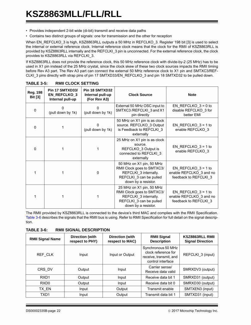
• Provides independent 2-bit wide (di-bit) transmit and receive data paths
• Contains two distinct groups of signals: one for transmission and the other for reception
When EN_REFCLKO_3 is high, KSZ8863RLL outputs a 50 MHz in REFCLKO_3. Register 198 bit [3] is used to selectthe internal or external reference clock. Internal reference clock means that the clock for the RMII of KSZ8863RLL isprovided by KSZ8863RLL internally and the REFCLKI_3 pin is unconnected. For the external reference clock, the clockprovides to KSZ8863RLL via REFCLKI_3.
If KSZ8863RLL does not provide the reference clock, this 50 MHz reference clock with divide-by-2 (25 MHz) has to beused in X1 pin instead of the 25 MHz crystal, since the clock skew of these two clock sources impacts the RMII timingbefore Rev A3 part. The Rev A3 part can connect the external 50 MHz reference clock to X1 pin and SMTXC3/REF-CLKI_3 pins directly with strap pins of pin 17 SMTXD33/EN_REFCLKO_3 and pin 18 SMTXD32 to be pulled down.
The RMII provided by KSZ8863RLL is connected to the device’s third MAC and complies with the RMII Specification.Table 3-6 describes the signals that the RMII bus is using. Refer to RMII Specification for full detail on the signal descrip-tion.
TABLE 3-5: RMII CLOCK SETTING
Reg. 198 Bit [3]
Pin 17 SMTXD33/EN_REFCLKO_3Internal pull-up
Pin 18 SMTXD32Internal pull-up
(For Rev A3)Clock Source Note
00
(pull down by 1k)0
(pull down by 1k)
External 50 MHz OSC input to SMTXC3 /REFCLKI_3 and X1
pin directly
EN_REFCLKO_3 = 0 to disable REFCLKO_3 for
better EMI
0 10
(pull down by 1k)
50 MHz on X1 pin is as clock source. REFCLKO_3 Output is Feedback to REFCLKI_3
externally
EN_REFCLKO_3 = 1 to enable REFCLKO_3
0 1 1
25 MHz on X1 pin is as clock source.
REFCLKO_3 Output is connected to REFCLKI_3
externally
EN_REFCLKO_3 = 1 to enable REFCLKO_3
1 1 0
50 MHz on X1 pin, 50 MHz RMII Clock goes to SMTXC3/
REFCLKI_3 internally.REFCLKI_3 can be pulled
down by a resistor.
EN_REFCLKO_3 = 1 to enable REFCLKO_3 and no
feedback to REFCLKI_3
1 1 1
25 MHz on X1 pin, 50 MHz RMII Clock goes to SMTXC3/
REFCLKI_3 internally.REFCLKI_3 can be pulled
down by a resistor.
EN_REFCLKO_3 = 1 to enable REFCLKO_3 and no
feedback to REFCLKI_3
TABLE 3-6: RMII SIGNAL DESCRIPTION
RMII Signal NameDirection (with respect to PHY)
Direction (with respect to MAC)
RMII Signal Description
KSZ8863RLL RMII Signal Direction
REF_CLK Input Input or Output
Synchronous 50 MHz clock reference for
receive, transmit, and control interface
REFCLKI_3 (input)
CRS_DV Output InputCarrier sense/
Receive data validSMRXDV3 (output)
RXD1 Output Input Receive data bit 1 SMRXD31 (output)
RXD0 Output Input Receive data bit 0 SMRXD30 (output)
TX_EN Input Output Transmit enable SMTXEN3 (input)
TXD1 Input Output Transmit data bit 1 SMTXD31 (input)
DS00002335B-page 22 2017 Microchip Technology Inc.
KSZ8863MLL/FLL/RLL
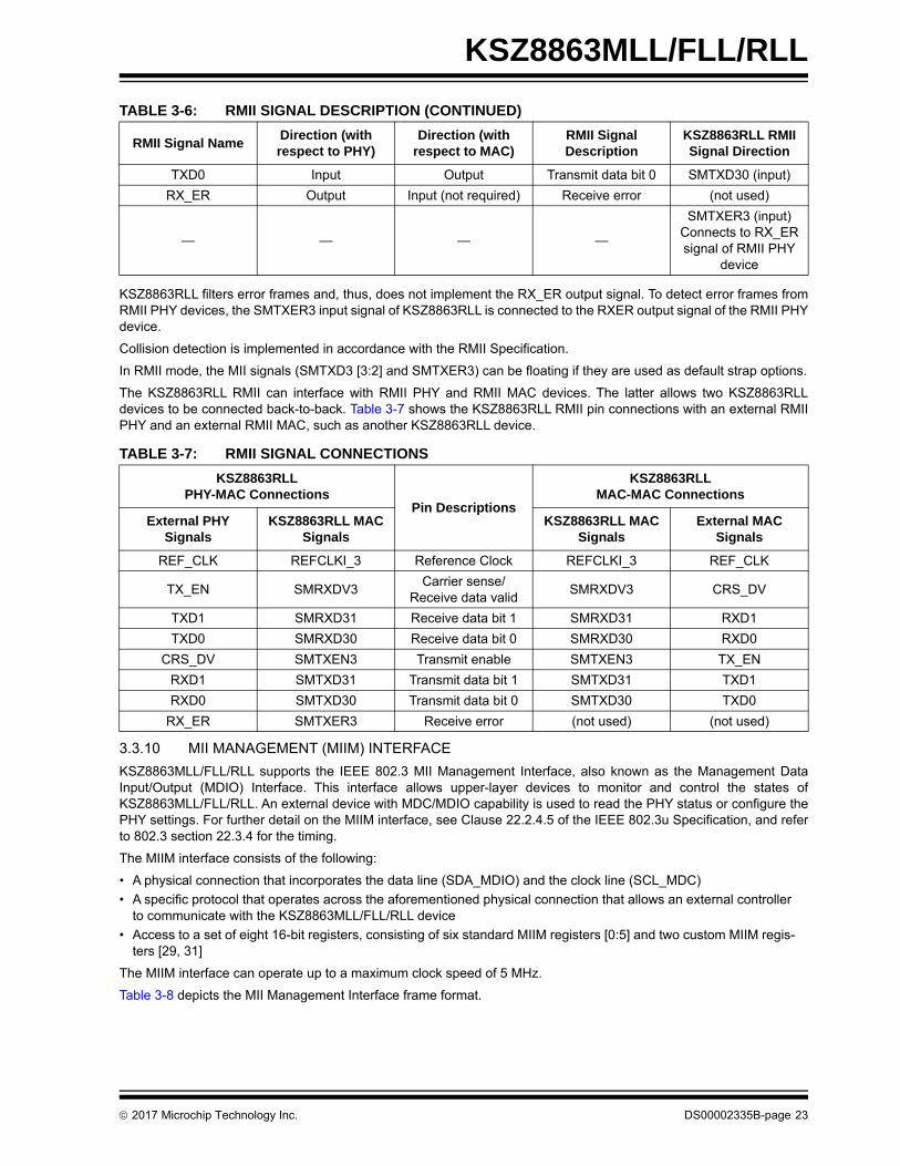
KSZ8863RLL filters error frames and, thus, does not implement the RX_ER output signal. To detect error frames fromRMII PHY devices, the SMTXER3 input signal of KSZ8863RLL is connected to the RXER output signal of the RMII PHYdevice.
Collision detection is implemented in accordance with the RMII Specification.
In RMII mode, the MII signals (SMTXD3 [3:2] and SMTXER3) can be floating if they are used as default strap options.
The KSZ8863RLL RMII can interface with RMII PHY and RMII MAC devices. The latter allows two KSZ8863RLLdevices to be connected back-to-back. Table 3-7 shows the KSZ8863RLL RMII pin connections with an external RMIIPHY and an external RMII MAC, such as another KSZ8863RLL device.
3.3.10 MII MANAGEMENT (MIIM) INTERFACE
KSZ8863MLL/FLL/RLL supports the IEEE 802.3 MII Management Interface, also known as the Management DataInput/Output (MDIO) Interface. This interface allows upper-layer devices to monitor and control the states ofKSZ8863MLL/FLL/RLL. An external device with MDC/MDIO capability is used to read the PHY status or configure thePHY settings. For further detail on the MIIM interface, see Clause 22.2.4.5 of the IEEE 802.3u Specification, and referto 802.3 section 22.3.4 for the timing.
The MIIM interface consists of the following:
• A physical connection that incorporates the data line (SDA_MDIO) and the clock line (SCL_MDC)
• A specific protocol that operates across the aforementioned physical connection that allows an external controller to communicate with the KSZ8863MLL/FLL/RLL device
• Access to a set of eight 16-bit registers, consisting of six standard MIIM registers [0:5] and two custom MIIM regis-ters [29, 31]
The MIIM interface can operate up to a maximum clock speed of 5 MHz.
Table 3-8 depicts the MII Management Interface frame format.
TXD0 Input Output Transmit data bit 0 SMTXD30 (input)
RX_ER Output Input (not required) Receive error (not used)
— — — —
SMTXER3 (input)Connects to RX_ER signal of RMII PHY
device
TABLE 3-7: RMII SIGNAL CONNECTIONS
KSZ8863RLLPHY-MAC Connections
Pin Descriptions
KSZ8863RLLMAC-MAC Connections
External PHY Signals
KSZ8863RLL MAC Signals
KSZ8863RLL MAC Signals
External MAC Signals
REF_CLK REFCLKI_3 Reference Clock REFCLKI_3 REF_CLK
TX_EN SMRXDV3Carrier sense/
Receive data validSMRXDV3 CRS_DV
TXD1 SMRXD31 Receive data bit 1 SMRXD31 RXD1
TXD0 SMRXD30 Receive data bit 0 SMRXD30 RXD0
CRS_DV SMTXEN3 Transmit enable SMTXEN3 TX_EN
RXD1 SMTXD31 Transmit data bit 1 SMTXD31 TXD1
RXD0 SMTXD30 Transmit data bit 0 SMTXD30 TXD0
RX_ER SMTXER3 Receive error (not used) (not used)
TABLE 3-6: RMII SIGNAL DESCRIPTION (CONTINUED)
RMII Signal NameDirection (with respect to PHY)
Direction (with respect to MAC)
RMII Signal Description
KSZ8863RLL RMII Signal Direction
2017 Microchip Technology Inc. DS00002335B-page 23
KSZ8863MLL/FLL/RLL
3.3.11 SERIAL MANAGEMENT INTERFACE (SMI)
The SMI is the KSZ8863MLL/FLL/RLL non-standard MIIM interface that provides access to all KSZ8863MLL/FLL/RLLconfiguration registers. This interface allows an external device to completely monitor and control the states ofKSZ8863MLL/FLL/RLL.
The SMI interface consists of the following:
• A physical connection that incorporates the data line (SDA_MDIO) and the clock line (SCL_MDC)
• A specific protocol that operates across the aforementioned physical connection that allows an external controller to communicate with the KSZ8863MLL/FLL/RLL device
• Access to all KSZ8863MLL/FLL/RLL configuration registers. Register access includes the Global, Port, and Advanced Control Registers 0-198 (0x00 – 0xC6), and indirect access to the standard MIIM registers [0:5] and custom MIIM registers [29, 31].
Table 3-9 depicts the SMI frame format.
SMI register read access is selected when OP Code is set to “00” and bit 4 of the PHY address is set to ‘1’. SMI registerwrite access is selected when OP Code is set to “00” and bit 4 of the PHY address is set to ‘0’. PHY address bit [3] isundefined for SMI register access, and hence can be set to either ‘0’ or ‘1’ in read or write operations.
To access the KSZ8873MLL/FLL/RLL registers 0-196 (0x00 – 0xC6), the following applies:
• PHYAD[2:0] and REGAD[4:0] are concatenated to form the 8-bit address; that is, PHYAD[2:0], REGAD[4:0] = bits [7:0] of the 8-bit address.
• TA bits [1:0] are ‘Z0’ that means the processor MDIO pin is changed to input Hi-Z from output mode and the fol-lowing ‘0’ is the read response from the device.
• TA bits [1:0] are set to ‘10’ when write registers.
• Registers are 8 data bits wide.
- For read operation, data bits [15:8] are read back as 0’s.
- For write operation, data bits [15:8] are not defined, and hence can be set to either ‘0’ or ‘1’.
The SMI register access is the same as the MIIM register access, except for the register access requirements presentedin this section.
3.4 Advanced Switch Functions
3.4.1 BYPASS MODE
KSZ8863MLL/FLL/RLL also offers a bypass mode that enables system-level power saving. When the CPU (connectedto port 3) enters a power saving mode of power down or sleeping mode, the CPU can control pin 24 SMTXER3/MII_LINK_3, which can be tied high so that KSZ8863MLL/FLL/RLL detects this change and automatically switches tothe bypass mode. In this mode, the switch function between port 1 and port 2 is sustained. The packets with DA to port3 are dropped and bypass the internal buffer memory, making the buffer memory more efficient for data transfer betweenport 1 and port 2.
TABLE 3-8: MII MANAGEMENT FRAME FORMAT
PreambleStart of Frame
Read/Write OP
Code
PHY Address Bits [4:0]
REG Address Bits [4:0]
TA Data Bits[15:0] Idle
Read 32 1’s 01 10 AAAAA RRRRR Z0 DDDDDDDD_DDDDDDDD Z
Write 32 1’s 01 01 AAAAA RRRRR 10 DDDDDDDD_DDDDDDDD Z
TABLE 3-9: SERIAL MANAGEMENT INTERFACE (SMI) FRAME FORMAT
PreambleStart of Frame
Read/Write OP
Code
PHY Address Bits [4:0]
REG Address Bits [4:0]
TA Data Bits [15:0] Idle
Read 32 1’s 01 00 1xRRR RRRRR Z0 0000_0000_DDDD_DDDD Z
Write 32 1’s 01 00 0xRRR RRRRR 10 xxxx_xxxx_DDDD_DDDD Z
DS00002335B-page 24 2017 Microchip Technology Inc.

KSZ8863MLL/FLL/RLL
3.4.2 IEEE 802.1Q VLAN SUPPORT
KSZ8863MLL/FLL/RLL supports 16 active VLANs out of the 4096 possible VLANs specified in the IEEE 802.1Q spec-ification. KSZ8863MLL/FLL/RLL provides a 16-entries VLAN table that converts the 12-bits VLAN ID (VID) to the 4-bitsFilter ID (FID) for address lookup. If a non-tagged or null-VID-tagged packet is received, the ingress port default VID isused for lookup. In VLAN mode, the lookup process starts with VLAN Table lookup to determine whether the VID is valid.If the VID is not valid, the packet is dropped and its address is not learned. If the VID is valid, the FID is retrieved forfurther lookup. The FID and Destination Address (FID+DA) are used to determine the destination port. The FID andSource Address (FID+SA) are used for address learning.
Advanced VLAN features, such as “Ingress VLAN filtering” and “Discard Non PVID packets,” are also supported byKSZ8863MLL/FLL/RLL. These features can be set on a per-port basis and are defined in register 18, 34, and 50 forports 1, 2, and 3, respectively.
3.4.3 QOS PRIORITY SUPPORT
KSZ8863MLL/FLL/RLL provides Quality of Service (QoS) for applications such as VoIP and video conferencing. Offer-ing four priority queues per port, the per-port transmit queue can be split into four priority queues: Queue 3 is the highestpriority queue and Queue 0 is the lowest priority queue. Bit [0] of registers 16, 32, and 48 is used to enable split transmitqueues for ports 1, 2, and 3, respectively. If a port's transmit queue is not split, high priority and low priority packets haveequal priority in the transmit queue.
There is an additional option to either always deliver high priority packets first or use weighted fair queuing for the fourpriority queues. This global option is set and explained in bit [3] of register 5.
3.4.4 PORT-BASED PRIORITY
With port-based priority, each ingress port is individually classified as a high priority receiving port. All packets receivedat the high-priority receiving port are marked as high priority and are sent to the high-priority transmit queue if the cor-responding transmit queue is split. Bits [4:3] of registers 16, 32, and 48 are used to enable port-based priority for ports1, 2, and 3, respectively.
3.4.5 802.1P-BASED PRIORITY
For 802.1p-based priority, KSZ8863MLL/FLL/RLL examines the ingress (incoming) packets to determine whether theyare tagged. If tagged, the 3-bit priority field in the VLAN tag is retrieved and compared against the “priority mapping”value, as specified by the registers 12 and 13. The “priority mapping” value is programmable.
TABLE 3-10: FID+DA LOOKUP IN VLAN MODE
DA Found in Static MAC
Table?
Use FID Flag?
FID Match?FID+DA Found in
Dynamic MAC Table?
Action
No Don’t care Don’t care NoBroadcast to the membership ports defined
in the VLAN Table bits [18:16]
No Don’t care Don’t care YesSend to the destination port defined in the Dynamic MAC Address Table bits [53:52]
Yes 0 Don’t care Don’t careSend to the destination port(s) defined in the Static MAC Address Table bits [50:48]
Yes 1 No NoBroadcast to the membership ports defined
in the VLAN Table bits [18:16]
Yes 1 No YesSend to the destination port defined in the Dynamic MAC Address Table bits [53:52]
Yes 1 Yes Don’t careSend to the destination port(s) defined in the Static MAC Address Table bits [50:48]
TABLE 3-11: FID+SA LOOKUP IN VLAN MODE
FID+SA Found in Dynamic MAC Table? Action
No Learn and add FID+SA to the Dynamic MAC Address Table
Yes Update time stamp
2017 Microchip Technology Inc. DS00002335B-page 25

KSZ8863MLL/FLL/RLL
Figure 3-6 illustrates how the 802.1p priority field is embedded in the 802.1Q VLAN tag.
The 802.1p-based priority is enabled with bit [5] of registers 16, 32, and 48 for ports 1, 2, and 3, respectively.
KSZ8863MLL/FLL/RLL provides the option to insert or remove the header of the priority tagged frame at each individualegress port. This header, consisting of the 2 bytes VLAN Protocol ID (VPID) and the 2-byte Tag Control Information field(TCI), is also referred to as the IEEE 802.1Q VLAN tag.
Tag Insertion is enabled by bit [2] of the port registers control 0 and the register 194 to select which source port (ingressport) PVID can be inserted on the egress port for ports 1, 2, and 3, respectively. At the egress port, untagged packetsare tagged with the ingress port’s default tag. The default tags are programmed in register sets 19,20, 35,36, and51,52 for ports 1, 2, and 3, respectively; and the source port VID has to be inserted at selected egress ports by bit [5:0]of register 194. KSZ8863MLL/FLL/RLL does not add tags to already tagged packets.
Tag Removal is enabled by bit [1] of registers 16, 32, and 48 for ports 1, 2, and 3, respectively. At the egress port, taggedpackets will have their 802.1Q VLAN Tags removed. KSZ8863MLL/FLL/RLL does not modify untagged packets.
The CRC is recalculated for both tag insertion and tag removal.
The 802.1p Priority Field Re-mapping is a QoS feature that allows KSZ8863MLL/FLL/RLL to set the “User Priority Ceil-ing” at any ingress port. If the ingress packet’s priority field has a higher priority value than the default tag’s priority fieldof the ingress port, the packet’s priority field is replaced with the default tag’s priority field.
3.4.6 DIFFSERV-BASED PRIORITY
DiffServ-based priority uses the ToS registers (registers 96 to 111) in the Advanced Control Registers section. The ToSpriority control registers implement a fully decoded, 64-bit Differentiated Services Code Point (DSCP) register to deter-mine packet priority from the 6-bit ToS field in the IP header. When the most significant 6 bits of the ToS field are fullydecoded, the resultant of the 64 possibilities is compared with the corresponding bits in the DSCP register to determinepriority.
3.5 Spanning Tree Support
To support spanning tree, port 3 is designated as the processor port.
The other ports (port 1 and port 2) can be configured in one of the five spanning tree states via “transmit enable,” “receiveenable,” and “learning disable” register settings in registers 18 and 34 for ports 1 and 2, respectively. Table 3-12 showsthe port setting and software actions taken for each of the five spanning tree states.
FIGURE 3-6: 802.1P PRIORITY FIELD FORMAT
Preamble DA TCI
8 6 6 2
length LLC Data FCS
2 46-1500 4
1
Tagged Packet Type(8100 for Ethernet) 802.1p C
FI VLAN ID
Bytes
Bits 16 3 12
802.1q VLAN Tag
2
SA VPID
DS00002335B-page 26 2017 Microchip Technology Inc.

KSZ8863MLL/FLL/RLL
3.6 Rapid Spanning Tree Support
There are three operational states of the Discarding, Learning, and Forwarding assigned to each port for RSTP:
Discarding ports do not participate in the active topology and do not learn MAC addresses.
Discarding state: The state includes three states of the disable, blocking, and listening of STP.
Port setting: “transmit enable = 0, receive enable = 0, learning disable = 1"
Software action: The processor should not send any packets to the port. The switch may still send specific packets tothe processor (packets that match some entries in the static table with “overriding bit” set), and the processor shoulddiscard those packets. When disabling the port’s learning capability (learning disable=’1’), set the register 2 bit 5 and bit4 flushes rapidly the port related entries in the dynamic MAC table and static MAC table.
Note: The processor is connected to port 3 via the MII interface. Address learning is disabled on the port in this state.
Ports in Learning states learn MAC addresses, but do not forward user traffic.
Learning state: Only packets to and from the processor are forwarded. Learning is enabled.
Port setting: “transmit enable = 0, receive enable = 0, learning disable = 0”
TABLE 3-12: SPANNING TREE STATES
Disable State Port Setting Software Action
The port should not for-ward or receive any pack-ets. Learning is disabled.
“transmit enable = 0, receive enable = 0, learning disable =1”
The processor should not send any packets to the port. The switch may still send specific packets to the processor (packets that match some entries in the “static MAC table” with “overrid-ing bit” set) and the processor should discard those packets. Address learning is disabled on the port in this state.
Blocking State Port Setting Software Action
Only packets to the pro-cessor are forwarded. Learning is disabled.
“transmit enable = 0, receive enable = 0, learning disable =1”
The processor should not send any packets to the port(s) in this state. The processor should program the “Static MAC table” with the entries that it needs to receive (for example, BPDU packets). The “overriding” bit should also be set so that the switch will forward those specific packets to the processor. Address learning is disabled on the port in this state.
Listening State Port Setting Software Action
Only packets to and from the processor are for-warded. Learning is dis-abled.
“transmit enable = 0, receive enable = 0, learning disable =1”
The processor should program the “Static MAC table” with the entries that it needs to receive (for example, BPDU packets). The “overriding” bit should be set so that the switch will forward those specific packets to the processor. The processor may send packets to the port(s) in this state. See Section 3.7, "Tail Tagging Mode" for details. Address learning is disabled on the port in this state.
Learning State Port Setting Software Action
Only packets to and from the processor are for-warded. Learning is enabled.
“transmit enable = 0, receive enable = 0,
learning disable = 0”
The processor should program the “Static MAC table” with the entries that it needs to receive (for example, BPDU packets). The “overriding” bit should be set so that the switch will forward those specific packets to the processor. The processor may send packets to the port(s) in this state. See Section 3.7, "Tail Tagging Mode" for details. Address learning is enabled on the port in this state.
Forwarding State Port Setting Software Action
Packets are forwarded and received normally. Learn-ing is enabled.
“transmit enable = 1, receive enable = 1, learning disable = 0”
The processor programs the “Static MAC table” with the entries that it needs to receive (for example, BPDU packets). The “overriding” bit is set so that the switch forwards those specific packets to the processor. The processor can send packets to the port(s) in this state. See Section 3.7, "Tail Tagging Mode" for details. Address learning is enabled on the port in this state.
2017 Microchip Technology Inc. DS00002335B-page 27
KSZ8863MLL/FLL/RLL
Software action: The processor should program the static MAC table with the entries that it needs to receive (for exam-ple, BPDU packets). The “overriding” bit should be set so that the switch forwards those specific packets to the proces-sor. The processor may send packets to the port(s) in this state, see Section 3.7, "Tail Tagging Mode" for details.Address learning is enabled on the port in this state.
Ports in Forwarding states fully participate in both data forwarding and MAC learning.
Forwarding state: Packets are forwarded and received normally. Learning is enabled.
Port setting: “transmit enable = 1, receive enable = 1, learning disable = 0”
Software action: The processor should program the static MAC table with the entries that it needs to receive (for exam-ple, BPDU packets). The “overriding” bit should be set so that the switch forwards those specific packets to the proces-sor. The processor may send packets to the port(s) in this state, see Section 3.7, "Tail Tagging Mode" for details.Address learning is enabled on the port in this state.
RSTP uses only one type of BPDU called RSTP BPDUs, which are similar to STP Configuration BPDUs with the excep-tion of a type field set to “version 2” for RSTP and “version 0” for STP, and a flag field carrying additional information.
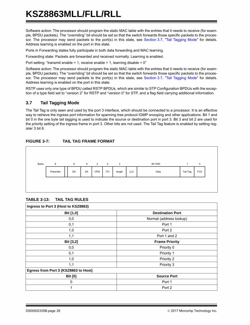
3.7 Tail Tagging Mode
The Tail Tag is only seen and used by the port 3 interface, which should be connected to a processor. It is an effectiveway to retrieve the ingress port information for spanning tree protocol IGMP snooping and other applications. Bit 1 andbit 0 in the one byte tail tagging is used to indicate the source or destination port in port 3. Bit 3 and bit 2 are used forthe priority setting of the ingress frame in port 3. Other bits are not used. The Tail Tag feature is enabled by setting reg-ister 3 bit 6.
FIGURE 3-7: TAIL TAG FRAME FORMAT
TABLE 3-13: TAIL TAG RULES
Ingress to Port 3 (Host to KSZ8863)
Bit [1,0] Destination Port
0,0 Normal (address lookup)
0,1 Port 1
1,0 Port 2
1,1 Port 1 and 2
Bit [3,2] Frame Priority
0,0 Priority 0
0,1 Priority 1
1,0 Priority 2
1,1 Priority 3
Egress from Port 3 (KSZ8863 to Host)
Bit [0] Source Port
0 Port 1
1 Port 2
Preamble DA TCI
8 6 6 2
length LLC Data Tail Tag
2 46-1500 1
FCS
4Bytes 2
SA VPID
DS00002335B-page 28 2017 Microchip Technology Inc.

KSZ8863MLL/FLL/RLL
3.8 IGMP Support
For Internet Group Management Protocol (IGMP) support in layer 2, KSZ8863MLL/FLL/RLL provides two components:
3.8.1 IGMP SNOOPING
KSZ8863MLL/FLL/RLL traps IGMP packets and forwards them only to the processor (port 3). The IGMP packets areidentified as IP packets (either Ethernet IP packets, or IEEE 802.3 SNAP IP packets) with IP version = 0x4 and protocolversion number = 0x2.
3.8.2 IGMP SEND BACK TO THE SUBSCRIBED PORT
Once the host responds to the received IGMP packet, the host should knows the original IGMP ingress port and sendback the IGMP packet to this port only. Otherwise this IGMP packet is broadcasted to all ports to downgrade the perfor-mance.
Enabling the tail tag mode, the host will know the IGMP packet received port from tail tag bits [0] and can send back theresponse IGMP packet to this subscribed port by setting the bits [1,0] in the tail tag. Enable “Tail tag mode” by settingregister 3 bit 6. The tail tag is removed automatically when the IGMP packet is sent out from the subscribed port.
3.9 Port Mirroring Support
KSZ8863MLL/FLL/RLL supports “Port Mirroring” as follows:
• “Receive only” mirror on a port
- All packets received on the port are mirrored on the sniffer port. For example, port 1 is programmed as the “receive sniff” and port 3 is programmed as the “sniffer port.” A packet received on port 1 is destined to port 2 after the internal lookup. KSZ8863MLL/FLL/RLL forwards the packet to both port 2 and port 3. KSZ8863MLL/FLL/RLL can also optionally forward “bad” received packets to the “sniffer port.”
• “Transmit only” mirror on a port
- All packets transmitted on the port are mirrored on the sniffer port. For example, port 1 is programmed as the “transmit sniff” and port 3 is programmed as the “sniffer port.” A packet received on port 2 is destined to port 1 after the internal lookup. KSZ8863MLL/FLL/RLL forwards the packet to both port 1 and port 3.
• “Receive and transmit” mirror on two ports
- All packets received on port A and transmitted on port B are mirrored on the sniffer port. To turn on the “AND” feature, set register 5 bit [0] to ‘1’. For example, port 1 is programmed as the “receive sniff,” port 2 is pro-grammed as the “transmit sniff,” and port 3 is programmed as the “sniffer port.” A packet received on port 1 is destined to port 2 after the internal lookup. KSZ8863MLL/FLL/RLL forwards the packet to both port 2 and port 3.
Multiple ports can be selected as the “receive sniff” or the “transmit sniff.” In addition, any port can be selected as the“sniffer port.” All these per-port features can be selected through registers 17, 33, and 49 for ports 1, 2, and 3, respec-tively.
3.10 Rate Limiting Support
KSZ8863MLL/FLL/RLL provides a fine resolution hardware rate limiting from 64 kbps to 99 Mbps. The rate step is64 kbps when the rate range is from 64 kbps to 960 kbps, and 1 Mbps for 1 Mbps to 100 Mbps (100BT) or to 10 Mbps(10BT) (refer to Data Rate Limit Table). The rate limit is independent on the “receive side” and on the “transmit side” ona per-port basis. For 10BASE-T, a rate setting above 10 Mbps means the rate is not limited. On the receive side, thedata receive rate for each priority at each port can be limited by setting up Ingress Rate Control Registers. On the trans-mit side, the data transmit rate for each priority queue at each port can be limited by setting up Egress Rate ControlRegisters. The size of each frame has options to include a minimum IFG (Inter Frame Gap) or a Preamble byte, in addi-tion to the data field (from packet DA to FCS).
For ingress rate limiting, KSZ8863MLL/FLL/RLL provides options to selectively choose frames from all types, multicast,broadcast, and flooded unicast frames. KSZ8863MLL/FLL/RLL counts the data rate from those selected type of frames.Packets are dropped at the ingress port when the data rate exceeds the specified rate limit.
For egress rate limiting, the Leaky Bucket algorithm is applied to each output priority queue for shaping output traffic.Inter frame gap is stretched on a per-frame base to generate smooth, non-burst egress traffic. The throughput of eachoutput priority queue is limited by the egress rate specified.
2017 Microchip Technology Inc. DS00002335B-page 29

KSZ8863MLL/FLL/RLL
If any egress queue receives more traffic than the specified egress rate throughput, packets may be accumulated in theoutput queue and packet memory. After the memory of the queue or the port is used up, packet dropping or flow controlis triggered. As a result of congestion, the actual egress rate may be dominated by flow control or dropping at the ingressend, and may be therefore slightly less than the specified egress rate.
To reduce congestion, it is a good practice to make sure the egress bandwidth exceeds the ingress bandwidth.
3.11 Unicast MAC Address Filtering
The unicast MAC address filtering function works in conjunction with the static MAC address table. First, the static MACaddress table is used to assign a dedicated MAC address to a specific port. If a unicast MAC address is not recordedin the static table, it is also not learned in the dynamic MAC table. KSZ8863MLL/FLL/RLL is then configured with theoption to either filter or forward unicast packets for an unknown MAC address. This option is enabled and configured inregister 14.
This function is useful in preventing the broadcast of unicast packets that could degrade the quality of the port in appli-cations such as voice over Internet Protocol (VoIP).
3.12 Configuration Interface
KSZ8863MLL/FLL/RLL can operate as both a managed switch and an unmanaged switch.
In unmanaged mode, KSZ8863MLL/FLL/RLL is typically programmed using an EEPROM. If no EEPROM is present,KSZ8863MLL/FLL/RLL is configured using its default register settings. Some default settings are configured via strap-in pin options. The strap-in pins are indicated in the “Pin Description and I/O Assignment” table.
3.12.1 I2C MASTER SERIAL BUS CONFIGURATION
With an additional I2C (“2-wire”) EEPROM, KSZ8863MLL/FLL/RLL can perform more advanced switch features like“broadcast storm protection” and “rate control” without the need of an external processor.
For the KSZ8863MLL/FLL/RLL I2C Master configuration, the EEPROM stores the configuration data for register 0 toregister 198 (as defined in the KSZ8863MLL/FLL/RLL register map) with the exception of the “Read Only” status regis-ters. After the deassertion of reset, KSZ8863MLL/FLL/RLL sequentially reads in the configuration data for all 199 reg-isters, starting from register 0.
The following is a sample procedure for programming KSZ8863MLL/FLL/RLL with a pre-configured EEPROM:
1. Connect KSZ8863MLL/FLL/RLL to the EEPROM by joining the SCL and SDA signals of the respective devices.
2. Enable I2C Master mode by setting the KSZ8863MLL/FLL/RLL strap-in pins, P2LED [1:0] to “00”.
3. Check to ensure that the KSZ8863MLL/FLL/RLL reset signal input (RSTN) is properly connected to the externalreset source at the board level.
4. Program the desired configuration data into the EEPROM.
5. Place the EEPROM on the board and power up the board.
FIGURE 3-8: EEPROM CONFIGURATION TIMING DIAGRAM
....
....
....
RST_N
SCL
SDA
tprgm<15 ms
DS00002335B-page 30 2017 Microchip Technology Inc.
KSZ8863MLL/FLL/RLL
6. Assert an active-low reset to the RSTN pin of KSZ8863MLL/FLL/RLL. After reset is deasserted, KSZ8863MLL/FLL/RLL begins reading the configuration data from the EEPROM. KSZ8863MLL/FLL/RLL checks that the firstbyte read from the EEPROM is “88”. If this value is correct, EEPROM configuration continues. If not, EEPROMconfiguration access is denied and all other data sent from the EEPROM is ignored by KSZ8863MLL/FLL/RLL.
3.12.2 I2C SLAVE SERIAL BUS CONFIGURATION
In managed mode, KSZ8863MLL/FLL/RLL can be configured as an I2C Slave device. In this mode, an I2C Masterdevice (external controller or CPU) has complete programming access to the KSZ8863MLL/FLL/RLL’s 198 registers.Programming access includes Global registers, Port registers, Advanced Control registers, and indirect access to the“Static MAC Table,” “VLAN Table,” “Dynamic MAC Table,” and “MIB Counters.” The tables and counters are indirectlyaccessed via registers 121 to 131.
In I2C Slave mode, KSZ8863MLL/FLL/RLL operates like other I2C Slave devices. Addressing the KSZ8863MLL/FLL/RLL’s 8-bit registers is similar to addressing the Microchip AT24C02 EEPROM’s memory locations. Details of I2C reador write operations and related timing information can be found in the AT24C02 data sheet.
Two fixed 8-bit device addresses are used to address KSZ8863MLL/FLL/RLL in I2C Slave mode: one for read operationand the other for write operation. The addresses are as follows:
• 1011_1111 <read>
• 1011_1110 <write>
The following is a sample procedure for programming KSZ8863MLL/FLL/RLL using the I2C Slave serial bus:
1. Enable I2C Slave mode by setting the KSZ8863MLL/FLL/RLL strap-in pins P2LED [1:0] to “01”.
2. Power up the board and assert reset to the KSZ8863MLL/FLL/RLL device. Configure the desired register settingsin KSZ8863MLL/FLL/RLL using the I2C write operation.
3. Read back and verify the register settings in KSZ8863MLL/FLL/RLL using the I2C read operation.
Some of the configuration settings, such as “Aging Enable,” “Auto Negotiation Enable,” “Force Speed,” and “Powerdown,” can be programmed after the switch has been started.
3.12.3 SPI SLAVE SERIAL BUS CONFIGURATION
In managed mode, KSZ8863MLL/FLL/RLL can be configured as an SPI slave device. In this mode, an SPI masterdevice (external controller or CPU) has complete programming access to the KSZ8863MLL/FLL/RLL’s 198 registers.Programming access includes Global registers, Port registers, Advanced Control registers, and indirect access to the“Static MAC Table,” “VLAN Table,” “Dynamic MAC Table,” and “MIB Counters”. The tables and counters are indirectlyaccessed via registers 121 to 131.
KSZ8863MLL/FLL/RLL supports two standard SPI commands: ‘0000_0011’ for data read and ‘0000_0010’ for datawrite. KSZ8863MLL/FLL/RLL also supports SPI multiple read and multiple write to expedite register read back and reg-ister configuration, respectively.
SPI multiple read is initiated when the master device continues to drive the KSZ8863MLL/FLL/RLL SPISN input pin (SPISlave Select signal) low after a byte (a register) is read. The KSZ8863MLL/FLL/RLL internal address counter incrementsautomatically to the next byte (next register) after the read. The next byte at the next register address is shifted out ontothe KSZ8863MLL/FLL/RLL SPIQ output pin. SPI multiple read continues until the SPI master device terminates it bydeasserting the SPISN signal to KSZ8863MLL/FLL/RLL.
Similarly, SPI multiple write is initiated when the master device continues to drive the KSZ8863MLL/FLL/RLL SPISNinput pin low after a byte (a register) is written. The KSZ8863MLL/FLL/RLL internal address counter increments auto-matically to the next byte (next register) after the write. The next byte that is sent from the master device to theKSZ8863MLL/FLL/RLL SDA input pin is written to the next register address. SPI multiple write continues until the SPImaster device terminates it by deasserting the SPISN signal to KSZ8863MLL/FLL/RLL.
For both SPI multiple read and multiple write, the KSZ8863MLL/FLL/RLL internal address counter wraps back to registeraddress zero once the highest register address is reached. This feature allows all 198 KSZ8863MLL/FLL/RLL registersto be read, or written with a single SPI command from any initial register address.
KSZ8863MLL/FLL/RLL can support SPI bus up to a maximum of 25 MHz. A high performance SPI master is recom-mended to prevent internal counter overflow.
The following is a sample procedure for programming KSZ8863MLL/FLL/RLL using the SPI bus:
1. At the board level, connect the KSZ8863MLL/FLL/RLL pins as follows (Table 3-14):
2017 Microchip Technology Inc. DS00002335B-page 31
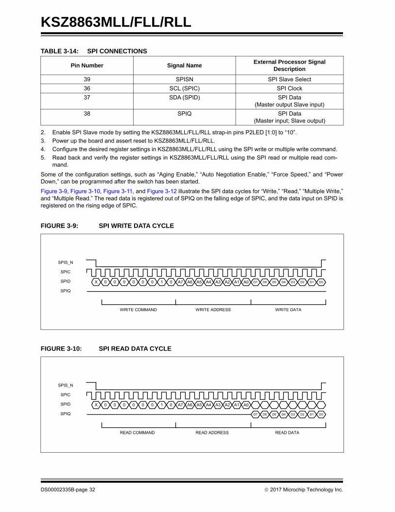
KSZ8863MLL/FLL/RLL
2. Enable SPI Slave mode by setting the KSZ8863MLL/FLL/RLL strap-in pins P2LED [1:0] to “10”.
3. Power up the board and assert reset to KSZ8863MLL/FLL/RLL.
4. Configure the desired register settings in KSZ8863MLL/FLL/RLL using the SPI write or multiple write command.
5. Read back and verify the register settings in KSZ8863MLL/FLL/RLL using the SPI read or multiple read com-mand.
Some of the configuration settings, such as “Aging Enable,” “Auto Negotiation Enable,” “Force Speed,” and “PowerDown,” can be programmed after the switch has been started.
Figure 3-9, Figure 3-10, Figure 3-11, and Figure 3-12 illustrate the SPI data cycles for “Write,” “Read,” “Multiple Write,”and “Multiple Read.” The read data is registered out of SPIQ on the falling edge of SPIC, and the data input on SPID isregistered on the rising edge of SPIC.
TABLE 3-14: SPI CONNECTIONS
Pin Number Signal NameExternal Processor Signal
Description
39 SPISN SPI Slave Select
36 SCL (SPIC) SPI Clock
37 SDA (SPID) SPI Data(Master output Slave input)
38 SPIQ SPI Data(Master input; Slave output)
FIGURE 3-9: SPI WRITE DATA CYCLE
FIGURE 3-10: SPI READ DATA CYCLE
SPIQ
SPIC
SPID
SPIS_N
0 0 0 0 0 0 1 0X A7 A6 A5 A4 A3 A2 A1 A0
WRITE COMMAND WRITE ADDRESS WRITE DATA
D2 D0D1D3D4D5D6D7
SPIQ
SPIC
SPID
SPIS_N
0 0 0 0 0 0 1 0X A7 A6 A5 A4 A3 A2 A1 A0
READ COMMAND READ ADDRESS READ DATA
D2 D0D1D3D4D5D6D7
DS00002335B-page 32 2017 Microchip Technology Inc.
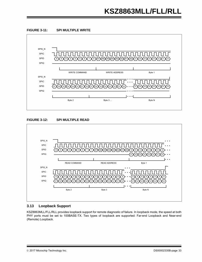
KSZ8863MLL/FLL/RLL
3.13 Loopback Support
KSZ8863MLL/FLL/RLL provides loopback support for remote diagnostic of failure. In loopback mode, the speed at bothPHY ports must be set to 100BASE-TX. Two types of loopback are supported: Far-end Loopback and Near-end(Remote) Loopback.
FIGURE 3-11: SPI MULTIPLE WRITE
FIGURE 3-12: SPI MULTIPLE READ
SPIQ
SPIC
SPID
SPIS_N
0 0 0 0 0 0 1 0X A7 A6 A5 A4 A3 A2 A1 A0
WRITE COMMAND WRITE ADDRESS Byte 1
D2 D0D1D3D4D5D6D7
SPIQ
SPIC
SPID
SPIS_N
D7 D6 D5 D4 D4 D2 D1 D0 D7 D6 D5 D4 D3 D2 D1 D0
Byte 2 Byte 3 ... Byte N
D2 D0D1D3D4D5D6D7
SPIQ
SPIC
SPID
SPIS_N
0 0 0 0 0 0 1 1X A7 A6 A5 A4 A3 A2 A1 A0
D7 D6 D5 D4 D3 D2 D1 D0
READ COMMAND READ ADDRESS Byte 1
X X X X X X X X X X X X X X X X
Byte 2 Byte 3 Byte N
X X X X X X X X
X X X X X X X X
D7 D6 D5 D4 D3 D2 D1 D0D7 D6 D5 D4 D3 D2 D1 D0 D7 D6 D5 D4 D3 D2 D1 D0SPIQ
SPIC
SPID
SPIS_N
2017 Microchip Technology Inc. DS00002335B-page 33

KSZ8863MLL/FLL/RLL
3.13.1 FAR-END LOOPBACK
Far-end loopback is conducted between KSZ8863MLL/FLL/RLL’s two PHY ports. The loopback is limited to few pack-ages a time for diagnostic purpose and cannot support large traffic. The loopback path starts at the “Originating” PHYport’s receive inputs (RXP/RXM), wraps around at the “loopback” PHY port’s PMD/PMA, and ends at the “Originating”PHY port’s transmit outputs (TXP/TXM).
Bit [0] of registers 29 and 45 is used to enable far-end loopback for ports 1 and 2, respectively. Alternatively, the MIIManagement register 0, bit [14] can be used to enable far-end loopback.
The far-end loopback path is illustrated in Figure 3-13.
3.13.2 NEAR-END (REMOTE) LOOPBACK
Near-end (Remote) loopback is conducted at either PHY port 1 or PHY port 2 of KSZ8863MLL/FLL/RLL. The loopbackpath starts at the PHY port’s receive inputs (RXPx/RXMx), wraps around at the same PHY port’s PMD/PMA, and endsat the PHY port’s transmit outputs (TXPx/TXMx).
Bit [1] of registers 26 and 42 is used to enable near-end loopback for ports 1 and 2, respectively. Alternatively, the MIIManagement register 31, bit [1] can be used to enable near-end loopback.
The near-end loopback paths are illustrated in Figure 3-14.
FIGURE 3-13: FAR-END LOOPBACK PATH
PMD/PMA
PCS
MAC
Switch
MAC
PCS
PMD/PMA
TXP /TXM
RXP /RXM
OriginatingPHY Port
Loop BackPHY Port
DS00002335B-page 34 2017 Microchip Technology Inc.

KSZ8863MLL/FLL/RLL
FIGURE 3-14: NEAR-END (REMOTE) LOOPBACK PATH
TXP1/TXM1
RXP1/RXM1
RXP2/RXM2
TXP2/TXM2
PHY Port 1
PHYPort 2
PMD/PMA
PCS
MAC
Switch
MAC
PCS
PMD/PMA
2017 Microchip Technology Inc. DS00002335B-page 35

KSZ8863MLL/FLL/RLL
4.0 REGISTER DESCRIPTIONS
4.1 MII Management (MIIM) Registers
The MIIM interface is used to access the MII PHY registers defined in this section. The SPI, I2C, and SMI interfaces canalso be used to access some of these registers. The latter three interfaces use a different mapping mechanism than theMIIM interface.
The “PHYADs” by default are assigned “0x1” for PHY1 (port 1) and “0x2” for PHY2 (port 2). Additionally, these “PHYADs”can be programmed to the PHY addresses specified in bits [7:3] of register 15 (0x0F): Global Control 13.
The “REGAD” supported are 0x0-0x5, 0x1D, and 0x1F.
TABLE 4-1: MIIM REGISTERS FOR KSZ8863MLL/FLL/RLL
Register Number Description
PHYAD = 0x1, REGAD = 0x0 PHY1 Basic Control Register
PHYAD = 0x1, REGAD = 0x1 PHY1 Basic Status Register
PHYAD = 0x1, REGAD = 0x2 PHY1 Physical Identifier I
PHYAD = 0x1, REGAD = 0x3 PHY1 Physical Identifier II
PHYAD = 0x1, REGAD = 0x4 PHY1 Auto-Negotiation Advertisement Register
PHYAD = 0x1, REGAD = 0x5 PHY1 Auto-Negotiation Link Partner Ability Register
PHYAD = 0x1, 0x6 – 0x1C PHY1 Not supported
PHYAD = 0x1, 0x1D PHY1 Not supported
PHYAD = 0x1, 0x1E PHY1 Not supported
PHYAD = 0x1, 0x1F PHY1 Special Control/Status
PHYAD = 0x2, REGAD = 0x0 PHY2 Basic Control Register
PHYAD = 0x2, REGAD = 0x1 PHY2 Basic Status Register
PHYAD = 0x2, REGAD = 0x2 PHY2 Physical Identifier I
PHYAD = 0x2, REGAD = 0x3 PHY2 Physical Identifier II
PHYAD = 0x2, REGAD = 0x4 PHY2 Auto-Negotiation Advertisement Register
PHYAD = 0x2, REGAD = 0x5 PHY2 Auto-Negotiation Link Partner Ability Register
PHYAD = 0x2, 0x6 – 0x1C PHY2 Not supported
PHYAD = 0x2, 0x1D PHY2 LinkMD Control/Status
PHYAD = 0x2, 0x1E PHY2 Not supported
PHYAD = 0x2, 0x1F PHY2 Special Control/Status
DS00002335B-page 36 2017 Microchip Technology Inc.

KSZ8863MLL/FLL/RLL
4.2 Register Descriptions
TABLE 4-2: REGISTER DESCRIPTIONS
Bit Name R/W Description Default Reference
PHY1 Register 0 (PHYAD = 0x1, REGAD = 0x0): MII Basic ControlPHY2 Register 0 (PHYAD = 0x2, REGAD = 0x0): MII Basic Control
15 Soft Reset RO Not Supported 0 —
14 Loopback R/W
1 = Perform loopback, as indicated:Port 1 Loopback (reg. 29, bit 0 = ‘1’)Start: RXP2/RXM2 (port 2)Loopback: PMD/PMA of port 1’s PHYEnd: TXP2/TXM2 (port 2)Port 2 Loopback (reg. 45, bit 0 = ‘1’)Start: RXP1/RXM1 (port 1)Loopback: PMD/PMA of port 2’s PHYEnd: TXP1/TXM1 (port 1)0 = Normal operation
0Reg. 29, bit 0Reg. 45, bit 0
13 Force 100 R/W1 = 100 Mbps0 = 10 Mbps
0Reg. 28, bit 6Reg. 44, bit 6
12 AN Enable R/W1 = Auto-negotiation enabled0 = Auto-negotiation disabled
1Reg. 28, bit 7Reg. 44, bit 7
11 Power Down R/W1 = Power down0 = Normal operation
0Reg. 29, bit 3Reg. 45, bit 3
10 Isolate RO Not Supported 0 —
9 Restart AN R/W1 = Restart auto-negotiation0 = Normal operation
0Reg. 29, bit 5Reg. 45, bit 5
8Force Full-Duplex
R/W1 = Full-duplex0 = Half-duplex
0Reg. 28, bit 5Reg. 44, bit 5
7 Collision Test RO Not Supported 0 —
6 Reserved RO — 0 —
5 Hp_mdix R/W1 = HP Auto MDI/MDI-X mode0 = Microchip Auto MDI/MDI-X mode
1Reg. 31, bit 7Reg. 47, bit 7
4 Force MDI R/W1 = Force MDI (transmit on RXP/RXM pins)0 = Normal operation (transmit on TXP/TXM pins)
0Reg. 29, bit 1Reg. 45, bit 1
3Disable MDIX
R/W1 = Disable auto MDI-X0 = Enable auto MDI-X
0Reg. 29, bit 2Reg. 45, bit 2
2Disable Far-End Fault
R/W1 = Disable far-end fault detection0 = Normal operation
0 Reg. 29, bit 4
1Disable Transmit
R/W1 = Disable transmit0 = Normal operation
0Reg. 29, bit 6Reg. 45, bit 6
0 Disable LED R/W1 = Disable LED0 = Normal operation
0Reg. 29, bit 7 Reg. 45, bit 7
PHY1 Register 1 (PHYAD = 0x1, REGAD = 0x1): MII Basic StatusPHY2 Register 1 (PHYAD = 0x2, REGAD = 0x1): MII Basic Status
15 T4 Capable RO 0 = Not 100BASE-T4 capable 0 —
14100 Full Capable
RO1 = 100BASE-TX full-duplex capable0 = Not capable of 100BASE-TX full-duplex
1 Always 1
13100 Half Capable
RO1 = 100BASE-TX half-duplex capable0 = Not 100BASE-TX half-duplex capable
1 Always 1
1210 Full Capable
RO1 = 10BASE-T full-duplex capable0 = Not 10BASE-T full-duplex capable
1 Always 1
2017 Microchip Technology Inc. DS00002335B-page 37

KSZ8863MLL/FLL/RLL
1110 Half Capable
RO1 = 10BASE-T half-duplex capable0 = Not 10BASE-T half-duplex capable
1 Always 1
10-7 Reserved RO — 0000 —
6Preamble Suppressed
RO Not Supported 0 —
5 AN Complete RO1 = Auto-negotiation complete0 = Auto-negotiation not completed
0Reg. 30, bit 6Reg. 46, bit 6
4Far-End Fault
RO1 = Far-end fault detected0 = No far-end fault detected
0 Reg. 31, bit 0
3 AN Capable RO1 = Auto-negotiation capable0 = Not auto-negotiation capable
1Reg. 28, bit 7Reg. 44, bit 7
2 Link Status RO1 = Link is up0 = Link is down
0Reg. 30, bit 5Reg. 46, bit 5
1 Jabber Test RO Not Supported 0 —
0Extended Capable
RO 0 = Not extended register capable 0 —
PHY1 Register 2 (PHYAD = 0x1, REGAD = 0x2): PHYID HighPHY2 Register 2 (PHYAD = 0x2, REGAD = 0x2): PHYID High
15-0 PHYID High RO High order PHYID bits 0x0022 —
PHY1 Register 3 (PHYAD = 0x1, REGAD = 0x3): PHYID LowPHY2 Register 3 (PHYAD = 0x2, REGAD = 0x3): PHYID Low
15-0 PHYID Low RO Low order PHYID bits 0x1430 —
PHY1 Register 4 (PHYAD = 0x1, REGAD = 0x4): Auto-Negotiation Advertisement AbilityPHY2 Register 4 (PHYAD = 0x2, REGAD = 0x4): Auto-Negotiation Advertisement Ability
15 Next Page RO Not Supported 0 —
14 Reserved RO — 0 —
13 Remote Fault RO Not Supported 0 —
12-11 Reserved RO — 00 —
10 Pause R/W1 = Advertise pause ability0 = Do not advertise pause ability
1Reg. 28, bit 4Reg. 44, bit 4
9 Reserved R/W — 0 —
8 Adv 100 Full R/W1 = Advertise 100 full-duplex ability0 = Do not advertise 100 full-duplex ability
1Reg. 28, bit 3Reg. 44, bit 3
7 Adv 100 Half R/W1 = Advertise 100 half-duplex ability0 = Do not advertise 100 half-duplex ability
1Reg. 28, bit 2Reg. 44, bit 2
6 Adv 10 Full R/W1 = Advertise 10 full-duplex ability0 = Do not advertise 10 full-duplex ability
1Reg. 28, bit 1Reg. 44, bit 1
5 Adv 10 Half R/W1 = Advertise 10 half-duplex ability0 = Do not advertise 10 half-duplex ability
1Reg. 28, bit 0Reg. 44, bit 0
4-0Selector Field
RO 802.3 00001 —
PHY1 Register 5 (PHYAD = 0x1, REGAD = 0x5): Auto-Negotiation Link Partner AbilityPHY2 Register 5 (PHYAD = 0x2, REGAD = 0x5): Auto-Negotiation Link Partner Ability
15 Next Page RO Not Supported 0 —
14 LP ACK RO Not Supported 0 —
13 Remote Fault RO Not Supported 0 —
12-11 Reserved RO — 00 —
TABLE 4-2: REGISTER DESCRIPTIONS (CONTINUED)
Bit Name R/W Description Default Reference
DS00002335B-page 38 2017 Microchip Technology Inc.
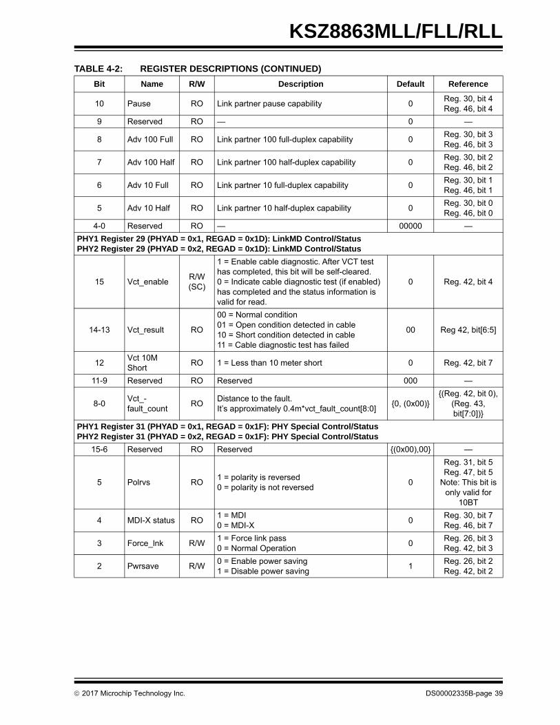
KSZ8863MLL/FLL/RLL
10 Pause RO Link partner pause capability 0Reg. 30, bit 4Reg. 46, bit 4
9 Reserved RO — 0 —
8 Adv 100 Full RO Link partner 100 full-duplex capability 0Reg. 30, bit 3Reg. 46, bit 3
7 Adv 100 Half RO Link partner 100 half-duplex capability 0Reg. 30, bit 2Reg. 46, bit 2
6 Adv 10 Full RO Link partner 10 full-duplex capability 0Reg. 30, bit 1Reg. 46, bit 1
5 Adv 10 Half RO Link partner 10 half-duplex capability 0Reg. 30, bit 0Reg. 46, bit 0
4-0 Reserved RO — 00000 —
PHY1 Register 29 (PHYAD = 0x1, REGAD = 0x1D): LinkMD Control/StatusPHY2 Register 29 (PHYAD = 0x2, REGAD = 0x1D): LinkMD Control/Status
15 Vct_enableR/W(SC)
1 = Enable cable diagnostic. After VCT test has completed, this bit will be self-cleared.0 = Indicate cable diagnostic test (if enabled) has completed and the status information is valid for read.
0 Reg. 42, bit 4
14-13 Vct_result RO
00 = Normal condition01 = Open condition detected in cable10 = Short condition detected in cable11 = Cable diagnostic test has failed
00 Reg 42, bit[6:5]
12Vct 10M Short
RO 1 = Less than 10 meter short 0 Reg. 42, bit 7
11-9 Reserved RO Reserved 000 —
8-0Vct_-fault_count
RODistance to the fault.It’s approximately 0.4m*vct_fault_count[8:0]
0, (0x00)(Reg. 42, bit 0),
(Reg. 43, bit[7:0])
PHY1 Register 31 (PHYAD = 0x1, REGAD = 0x1F): PHY Special Control/StatusPHY2 Register 31 (PHYAD = 0x2, REGAD = 0x1F): PHY Special Control/Status
15-6 Reserved RO Reserved (0x00),00 —
5 Polrvs RO1 = polarity is reversed0 = polarity is not reversed
0
Reg. 31, bit 5Reg. 47, bit 5
Note: This bit isonly valid for
10BT
4 MDI-X status RO1 = MDI 0 = MDI-X
0Reg. 30, bit 7Reg. 46, bit 7
3 Force_lnk R/W1 = Force link pass0 = Normal Operation
0Reg. 26, bit 3Reg. 42, bit 3
2 Pwrsave R/W0 = Enable power saving1 = Disable power saving
1Reg. 26, bit 2Reg. 42, bit 2
TABLE 4-2: REGISTER DESCRIPTIONS (CONTINUED)
Bit Name R/W Description Default Reference
2017 Microchip Technology Inc. DS00002335B-page 39
KSZ8863MLL/FLL/RLL
4.3 Memory Map (8-Bit Registers)
1Remote Loopback
R/W
1 = Perform Remote loopback, as follows: Port 1 (reg. 26, bit 1 = ‘1’)Start: RXP1/RXM1 (port 1)Loopback: PMD/PMA of port 1’s PHYEnd: TXP1/TXM1 (port 1)Port 2 (reg. 42, bit 1 = ‘1’)Start: RXP2/RXM2 (port 2)Loopback: PMD/PMA of port 2’s PHYEnd: TXP2/TXM2 (port 2)0 = Normal Operation
0Reg. 26, bit 1Reg. 42, bit 1
0 Reserved R/WReservedDo not change the default value.
0 —
TABLE 4-3: GLOBAL REGISTERS
Register (Decimal) Register (Hex) Description
0-1 0x00-0x01 Chip ID Register
2-15 0x02-0x0F Global Control Register
TABLE 4-4: PORT REGISTERS
Register (Decimal) Register (Hex) Description
16-29 0x10-0x1D Port 1 Control Registers, including MII PHY Registers
30-31 0x1E-0x1F Port 1 Status Registers, including MII PHY Registers
32-45 0x20-0x2D Port 2 Control Registers, including MII PHY Registers
46-47 0x2E-0x2F Port 2 Status Registers, including MII PHY Registers
48-57 0x30-0x39 Port 3 Control Registers
58-62 0x3A-0x3E Reserved
63 0x3F Port 3 Status Register
64-95 0x40-0x5F Reserved
TABLE 4-5: ADVANCED CONTROL REGISTERS
Register (Decimal) Register (Hex) Description
96-111 0x60-0x6F TOS Priority Control Registers
112-117 0x70-0x75 Switch Engine’s MAC Address Registers
118-120 0x76-0x78 User Defined Registers
121-122 0x79-0x7A Indirect Access Control Registers
123-131 0x7B-0x83 Indirect Data Registers
142-153 0x8E-0x99 Station Address
154-165 0x9A-0xA5 Egress Data Rate Limit
166 0xA6 Device Mode Indicator
167-170 0xA7-0xAA High Priority Packet Buffer Reserved
171-174 0xAB-0xAE PM Usage Flow Control Select Mode
175-186 0xAF-0xBA TXQ Split
187-188 0xBB-0xBC Link Change Interrupt Register
189 0xBD Force Pause Off Iteration Limit Enable
TABLE 4-2: REGISTER DESCRIPTIONS (CONTINUED)
Bit Name R/W Description Default Reference
DS00002335B-page 40 2017 Microchip Technology Inc.
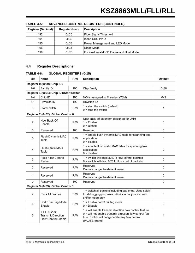
KSZ8863MLL/FLL/RLL
4.4 Register Descriptions
192 0xC0 Fiber Signal Threshold
194 0xC2 Insert SRC PVID
195 0xC3 Power Management and LED Mode
196 0xC4 Sleep Mode
198 0xC6 Forward Invalid VID Frame and Host Mode
TABLE 4-6: GLOBAL REGISTERS (0-15)
Bit Name R/W Description Default
Register 0 (0x00): Chip ID0
7-0 Family ID RO Chip family 0x88
Register 1 (0x01): Chip ID1/Start Switch
7-4 Chip ID RO 0x3 is assigned to M series. (73M) 0x3
3-1 Revision ID RO Revision ID —
0 Start Switch R/W1 = start the switch (default)0 = stop the switch
1
Register 2 (0x02): Global Control 0
7New Back-Off Enable
R/WNew back-off algorithm designed for UNH1 = Enable0 = Disable
0
6 Reserved RO Reserved 0
5Flush Dynamic MAC Table
R/W1 = enable flush dynamic MAC table for spanning tree application0 = disable
0
4Flush Static MAC Table
R/W1 = enable flush static MAC table for spanning tree application0 = disable
0
3Pass Flow Control Packet
R/W1 = switch will pass 802.1x flow control packets0 = switch will drop 802.1x flow control packets
0
2 Reserved R/WReservedDo not change the default value.
0
1 Reserved R/WReservedDo not change the default value.
0
0 Reserved RO Reserved 0
Register 3 (0x03): Global Control 1
7 Pass All Frames R/W1 = switch all packets including bad ones. Used solely for debugging purposes. Works in conjunction with sniffer mode only.
0
6Port 3 Tail Tag Mode Enable
R/W1 = Enable port 3 tail tag mode.0 = Disable.
0
5IEEE 802.3x Transmit Direction Flow Control Enable
R/W
1 = will enable transmit direction flow control feature.0 = will not enable transmit direction flow control fea-ture. Switch will not generate any flow control (PAUSE) frame.
1
TABLE 4-5: ADVANCED CONTROL REGISTERS (CONTINUED)
Register (Decimal) Register (Hex) Description
2017 Microchip Technology Inc. DS00002335B-page 41

KSZ8863MLL/FLL/RLL
4IEEE 802.3x Receive Direction Flow Control Enable
R/W
1 = will enable receive direction flow control feature.0 = will not enable receive direction flow control fea-ture. Switch will not react to any flow control (PAUSE) frame it receives.
1
3Frame Length Field Check
R/W
1 = will check frame length field in the IEEE packets. If the actual length does not match, the packet will be dropped (for Length/Type field < 1500).0 = will not check
0
2 Aging Enable R/W1 = enable age function in the chip0 = disable age function in the chip
1
1 Fast Age Enable R/W 1 = turn on fast age (800 µs) 0
0Aggressive Back-Off Enable
R/W1 = enable more aggressive back off algorithm in half-duplex mode to enhance performance. This is not an IEEE standard.
0
Register 4 (0x04): Global Control 2
7Unicast Port-VLAN Mismatch Discard
R/W
This feature is used with port-VLAN (described in reg. 17, reg. 33, etc.)1 = all packets can not cross VLAN boundary0 = unicast packets (excluding unknown/multicast/ broadcast) can cross VLAN boundaryNote: Port mirroring is not supported if this bit is set to “0”.
1
6Multicast Storm Protection Disable
R/W
1 = Broadcast Storm Protection does not include multicast packets. Only DA = FF-FF-FF-FF-FF-FF packets will be regulated.0 = Broadcast Storm Protection includes DA = FF-FF-FF-FF-FF-FF and DA[40] = 1 packets.
1
5 Back Pressure Mode R/W1 = carrier sense based back pressure is selected0 = collision based back pressure is selected
1
4Flow Control and Back Pressure Fair Mode
R/W
1 = Fair mode is selected. In this mode, if a flow con-trol port and a non-flow control port talk to the same destination port, packets from the non-flow control port may be dropped. This is to prevent the flow con-trol port from being flow controlled for an extended period of time.0 = In this mode, if a flow control port and a non-flow control port talk to the same destination port, the flow control port will be flow controlled. This may not be “fair” to the flow control port.
1
3No Excessive Collision Drop
R/W
1 = the switch will not drop packets when 16 or more collisions occur.0 = the switch will drop packets when 16 or more colli-sions occur.
0
2Huge Packet Support
R/W
1 = will accept packet sizes up to 1916 bytes (inclu-sive). This bit setting will override setting from bit 1 of this register.0 = the max packet size will be determined by bit 1 of this register.
0
1Legal Maximum Packet Size Check Enable
R/W
0 = will accept packet sizes up to 1536 bytes (inclu-sive).1 = 1522 bytes for tagged packets, 1518 bytes for untagged packets. Any packets larger than the speci-fied value will be dropped.
0
TABLE 4-6: GLOBAL REGISTERS (0-15) (CONTINUED)
Bit Name R/W Description Default
DS00002335B-page 42 2017 Microchip Technology Inc.
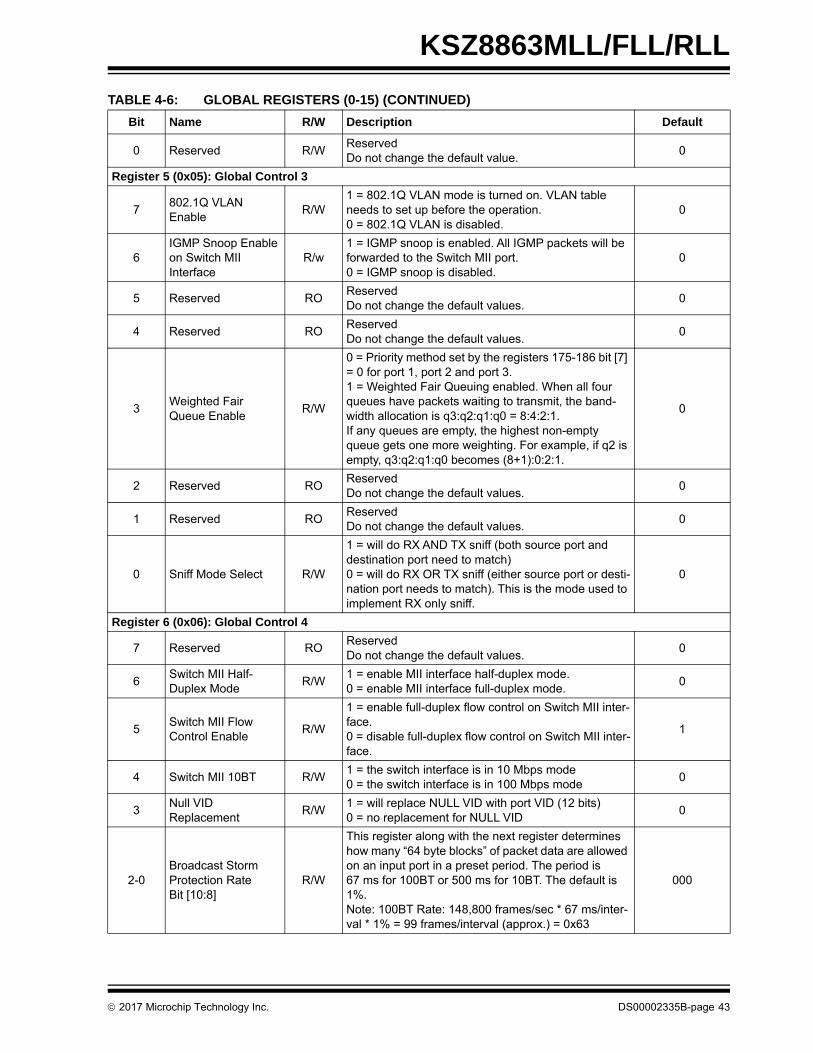
KSZ8863MLL/FLL/RLL
0 Reserved R/WReservedDo not change the default value.
0
Register 5 (0x05): Global Control 3
7802.1Q VLAN Enable
R/W1 = 802.1Q VLAN mode is turned on. VLAN table needs to set up before the operation.0 = 802.1Q VLAN is disabled.
0
6IGMP Snoop Enable on Switch MII Interface
R/w1 = IGMP snoop is enabled. All IGMP packets will be forwarded to the Switch MII port.0 = IGMP snoop is disabled.
0
5 Reserved ROReservedDo not change the default values.
0
4 Reserved ROReservedDo not change the default values.
0
3Weighted Fair Queue Enable
R/W
0 = Priority method set by the registers 175-186 bit [7] = 0 for port 1, port 2 and port 3.1 = Weighted Fair Queuing enabled. When all four queues have packets waiting to transmit, the band-width allocation is q3:q2:q1:q0 = 8:4:2:1.If any queues are empty, the highest non-empty queue gets one more weighting. For example, if q2 is empty, q3:q2:q1:q0 becomes (8+1):0:2:1.
0
2 Reserved ROReservedDo not change the default values.
0
1 Reserved ROReservedDo not change the default values.
0
0 Sniff Mode Select R/W
1 = will do RX AND TX sniff (both source port and destination port need to match)0 = will do RX OR TX sniff (either source port or desti-nation port needs to match). This is the mode used to implement RX only sniff.
0
Register 6 (0x06): Global Control 4
7 Reserved ROReservedDo not change the default values.
0
6Switch MII Half-Duplex Mode
R/W1 = enable MII interface half-duplex mode.0 = enable MII interface full-duplex mode.
0
5Switch MII Flow Control Enable
R/W
1 = enable full-duplex flow control on Switch MII inter-face.0 = disable full-duplex flow control on Switch MII inter-face.
1
4 Switch MII 10BT R/W1 = the switch interface is in 10 Mbps mode0 = the switch interface is in 100 Mbps mode
0
3Null VID Replacement
R/W1 = will replace NULL VID with port VID (12 bits)0 = no replacement for NULL VID
0
2-0Broadcast Storm Protection RateBit [10:8]
R/W
This register along with the next register determines how many “64 byte blocks” of packet data are allowed on an input port in a preset period. The period is 67 ms for 100BT or 500 ms for 10BT. The default is 1%.Note: 100BT Rate: 148,800 frames/sec * 67 ms/inter-val * 1% = 99 frames/interval (approx.) = 0x63
000
TABLE 4-6: GLOBAL REGISTERS (0-15) (CONTINUED)
Bit Name R/W Description Default
2017 Microchip Technology Inc. DS00002335B-page 43

KSZ8863MLL/FLL/RLL
Register 7 (0x07): Global Control 5
7-0Broadcast Storm Protection RateBit [7:0]
R/W
This register along with the previous register deter-mines how many “64 byte blocks” of packet data are allowed on an input port in a preset period. The period is 67 ms for 100BT or 500 ms for 10BT. The default is 1%.Note: 100BT Rate: 148,800 frames/sec * 67 ms/inter-val * 1% = 99 frames/interval (approx.) = 0x63
0x63
Register 8 (0x08): Global Control 6
7-0 Factory Testing ROReservedDo not change the default values.
0x00
Register 9 (0x09): Global Control 7
7-0 Factory Testing ROReservedDo not change the default values.
0x24
Register 10 (0x0A): Global Control 8
7-0 Factory Testing ROReservedDo not change the default values.
0x35
Register 11 (0x0B): Global Control 9
7-6CPU interface Clock Selection
R/W
00 = 31.25 MHz supports SPI speed below 6 MHz01 = 62.5 MHz supports SPI speed between 6 MHz to 12.5 MHz10 = 125 MHz supports SPI speed above 12.5 MHzNote: Lower clock speed will save more power con-sumption, It is better set to 31.25 MHz if SPI doesn’t request a high speed.
10
5-4 Reserved RO N/A Don’t Change 00
3-2 Reserved RO N/A Don’t Change 10
1 Reserved RO N/A Don’t Change 0
0 Reserved RO N/A Don’t Change 0
Register 12 (0x0C): Global Control 10
7-6 Tag_0x3 R/WIEEE 802.1p mapping. The value in this field is used as the frame’s priority when its IEEE 802.1p tag has a value of 0x3.
01
5-4 Tag_0x2 R/WIEEE 802.1p mapping. The value in this field is used as the frame’s priority when its IEEE 802.1p tag has a value of 0x2.
01
3-2 Tag_0x1 R/WIEEE 802.1p mapping. The value in this field is used as the frame’s priority when its IEEE 802.1p tag has a value of 0x1.
00
1-0 Tag_0x0 R/WIEEE 802.1p mapping. The value in this field is used as the frame’s priority when its IEEE 802.1p tag has a value of 0x0.
00
Register 13 (0x0D): Global Control 11
7-6 Tag_0x7 R/WIEEE 802.1p mapping. The value in this field is used as the frame’s priority when its IEEE 802.1p tag has a value of 0x7.
11
5-4 Tag_0x6 R/WIEEE 802.1p mapping. The value in this field is used as the frame’s priority when its IEEE 802.1p tag has a value of 0x6.
11
TABLE 4-6: GLOBAL REGISTERS (0-15) (CONTINUED)
Bit Name R/W Description Default
DS00002335B-page 44 2017 Microchip Technology Inc.
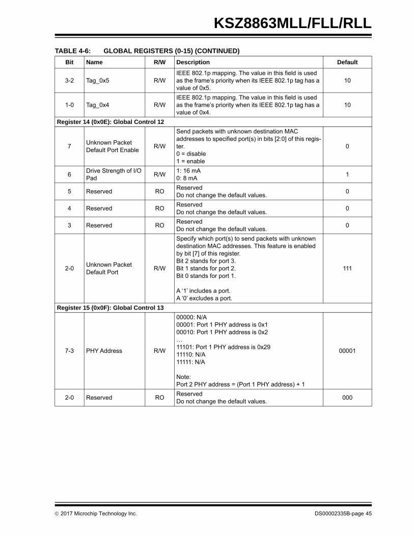
KSZ8863MLL/FLL/RLL
3-2 Tag_0x5 R/WIEEE 802.1p mapping. The value in this field is used as the frame’s priority when its IEEE 802.1p tag has a value of 0x5.
10
1-0 Tag_0x4 R/WIEEE 802.1p mapping. The value in this field is used as the frame’s priority when its IEEE 802.1p tag has a value of 0x4.
10
Register 14 (0x0E): Global Control 12
7Unknown Packet Default Port Enable
R/W
Send packets with unknown destination MAC addresses to specified port(s) in bits [2:0] of this regis-ter.0 = disable1 = enable
0
6Drive Strength of I/O Pad
R/W1: 16 mA0: 8 mA
1
5 Reserved ROReservedDo not change the default values.
0
4 Reserved ROReservedDo not change the default values.
0
3 Reserved ROReservedDo not change the default values.
0
2-0Unknown Packet Default Port
R/W
Specify which port(s) to send packets with unknown destination MAC addresses. This feature is enabled by bit [7] of this register.Bit 2 stands for port 3.Bit 1 stands for port 2.Bit 0 stands for port 1.
A ‘1’ includes a port.A ‘0’ excludes a port.
111
Register 15 (0x0F): Global Control 13
7-3 PHY Address R/W
00000: N/A00001: Port 1 PHY address is 0x100010: Port 1 PHY address is 0x2…11101: Port 1 PHY address is 0x2911110: N/A11111: N/A
Note:Port 2 PHY address = (Port 1 PHY address) + 1
00001
2-0 Reserved ROReservedDo not change the default values.
000
TABLE 4-6: GLOBAL REGISTERS (0-15) (CONTINUED)
Bit Name R/W Description Default
2017 Microchip Technology Inc. DS00002335B-page 45
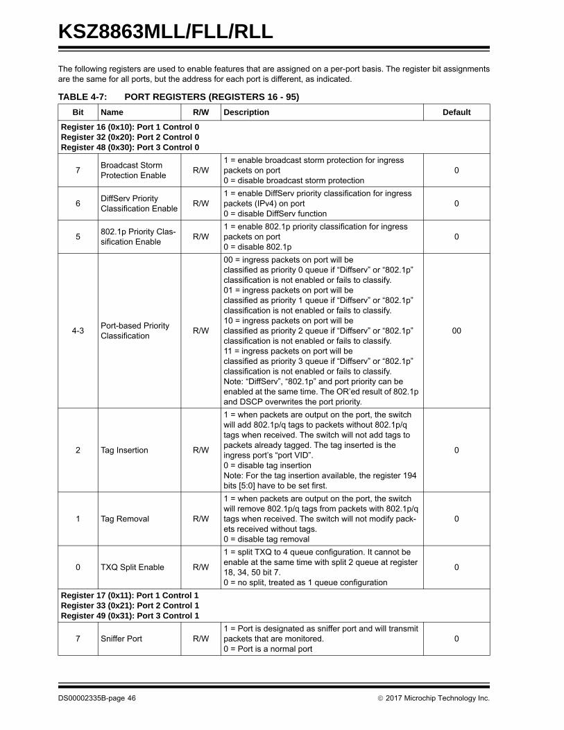
KSZ8863MLL/FLL/RLL
The following registers are used to enable features that are assigned on a per-port basis. The register bit assignmentsare the same for all ports, but the address for each port is different, as indicated.
TABLE 4-7: PORT REGISTERS (REGISTERS 16 - 95)
Bit Name R/W Description Default
Register 16 (0x10): Port 1 Control 0Register 32 (0x20): Port 2 Control 0Register 48 (0x30): Port 3 Control 0
7Broadcast Storm Protection Enable
R/W1 = enable broadcast storm protection for ingress packets on port0 = disable broadcast storm protection
0
6DiffServ Priority Classification Enable
R/W1 = enable DiffServ priority classification for ingress packets (IPv4) on port0 = disable DiffServ function
0
5802.1p Priority Clas-sification Enable
R/W1 = enable 802.1p priority classification for ingress packets on port0 = disable 802.1p
0
4-3Port-based Priority Classification
R/W
00 = ingress packets on port will beclassified as priority 0 queue if “Diffserv” or “802.1p” classification is not enabled or fails to classify.01 = ingress packets on port will be classified as priority 1 queue if “Diffserv” or “802.1p” classification is not enabled or fails to classify.10 = ingress packets on port will beclassified as priority 2 queue if “Diffserv” or “802.1p” classification is not enabled or fails to classify.11 = ingress packets on port will be classified as priority 3 queue if “Diffserv” or “802.1p” classification is not enabled or fails to classify.Note: “DiffServ”, “802.1p” and port priority can be enabled at the same time. The OR’ed result of 802.1p and DSCP overwrites the port priority.
00
2 Tag Insertion R/W
1 = when packets are output on the port, the switch will add 802.1p/q tags to packets without 802.1p/q tags when received. The switch will not add tags to packets already tagged. The tag inserted is the ingress port’s “port VID”.0 = disable tag insertionNote: For the tag insertion available, the register 194 bits [5:0] have to be set first.
0
1 Tag Removal R/W
1 = when packets are output on the port, the switch will remove 802.1p/q tags from packets with 802.1p/q tags when received. The switch will not modify pack-ets received without tags.0 = disable tag removal
0
0 TXQ Split Enable R/W
1 = split TXQ to 4 queue configuration. It cannot be enable at the same time with split 2 queue at register 18, 34, 50 bit 7.0 = no split, treated as 1 queue configuration
0
Register 17 (0x11): Port 1 Control 1Register 33 (0x21): Port 2 Control 1Register 49 (0x31): Port 3 Control 1
7 Sniffer Port R/W1 = Port is designated as sniffer port and will transmit packets that are monitored.0 = Port is a normal port
0
DS00002335B-page 46 2017 Microchip Technology Inc.

KSZ8863MLL/FLL/RLL
6 Receive Sniff R/W
1 = All packets received on the port will be marked as “monitored packets” and forwarded to the designated “sniffer port”0 = no receive monitoring
0
5 Transmit Sniff R/W
1 = All packets transmitted on the port will be marked as “monitored packets” and forwarded to the desig-nated “sniffer port”0 = no transmit monitoring
0
4 Double Tag R/W
1 = All packets will be tagged with port default tag of ingress port regardless of the original packets are tagged or not0 = do not double tagged on all packets
0
3 User Priority Ceiling R/W
1 = if the packet’s “user priority field” is greater than the “user priority field” in the port default tag register, replace the packet’s “user priority field” with the “user priority field” in the port default tag register.0 = do not compare and replace the packet’s ‘user pri-ority field”
0
2-0Port VLAN Membership
R/W
Define the port’s egress port VLAN membership. The port can only communicate within the membership. Bit 2 stands for port 3, bit 1 stands for port 2, bit 0 stands for port 1.An ‘1’ includes a port in the membership.An ‘0’ excludes a port from membership.
111
Register 18 (0x12): Port 1 Control 2Register 34 (0x22): Port 2 Control 2Register 50 (0x32): Port 3 Control 2
7Enable 2 Queue Split of Tx Queue
R/W
1 = EnableIt cannot be enable at the same time with split 4 queue at register 16, 32, and 48 bit 0.0 = Disable
0
6Ingress VLAN Filtering
R/W
1 = the switch will discard packets whose VID port membership in VLAN table bits [18:16] does not include the ingress port.0 = no ingress VLAN filtering.
0
5Discard non-PVID Packets
R/W1 = the switch will discard packets whose VID does not match ingress port default VID.0 = no packets will be discarded
0
4 Force Flow Control R/W
1 = will always enable full-duplex flow control on the port, regardless of AN result.0 = full-duplex flow control is enabled based on AN result.
Pin value during reset:
For port 1, SPIQ pin (default is
PD)For port 2,
SMRXD30 pinFor port 3, this
bit has no meaning. Flow
Control is set by Reg. 6, bit 5.
3Back Pressure Enable
R/W1 = enable port’s half-duplex back pressure0 = disable port’s half-duplex back pressure
0
TABLE 4-7: PORT REGISTERS (REGISTERS 16 - 95) (CONTINUED)
Bit Name R/W Description Default
2017 Microchip Technology Inc. DS00002335B-page 47
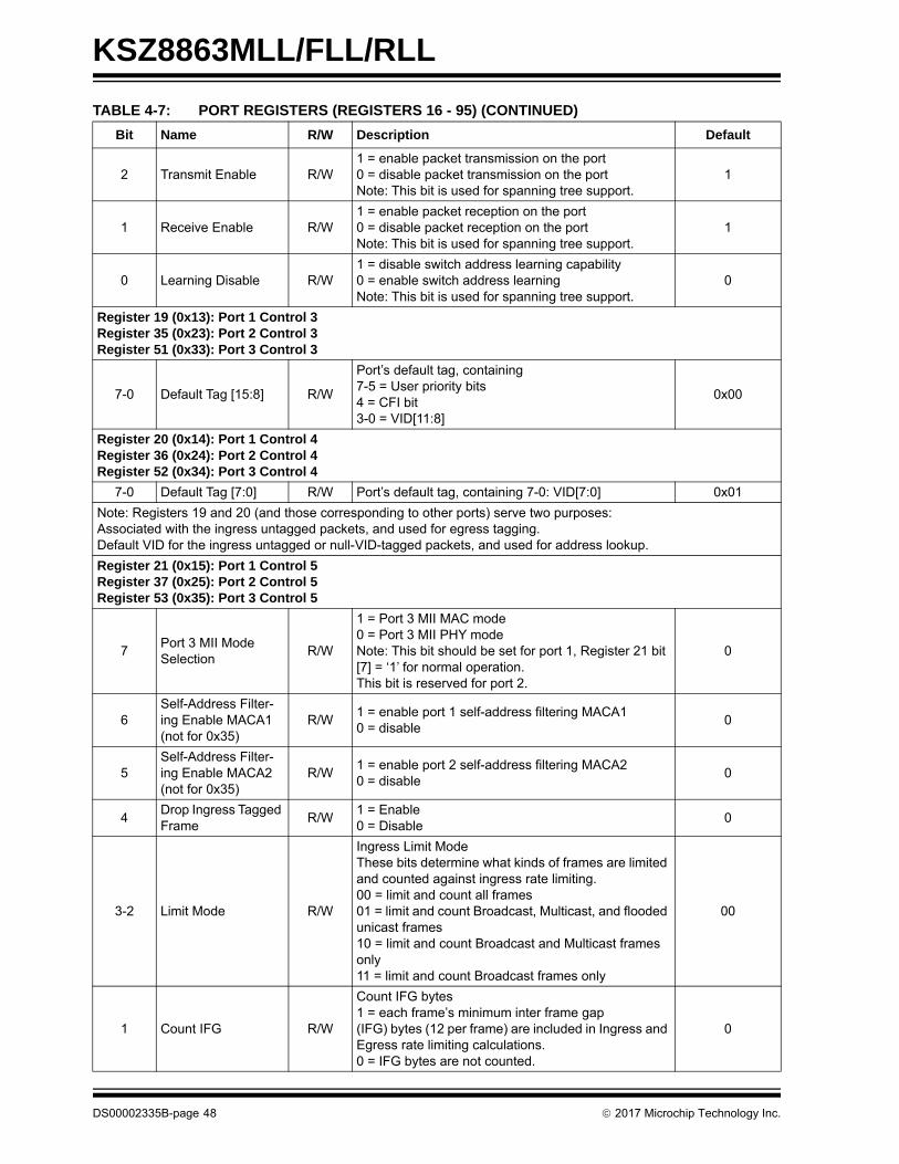
KSZ8863MLL/FLL/RLL
2 Transmit Enable R/W1 = enable packet transmission on the port0 = disable packet transmission on the portNote: This bit is used for spanning tree support.
1
1 Receive Enable R/W1 = enable packet reception on the port0 = disable packet reception on the portNote: This bit is used for spanning tree support.
1
0 Learning Disable R/W1 = disable switch address learning capability0 = enable switch address learningNote: This bit is used for spanning tree support.
0
Register 19 (0x13): Port 1 Control 3Register 35 (0x23): Port 2 Control 3Register 51 (0x33): Port 3 Control 3
7-0 Default Tag [15:8] R/W
Port’s default tag, containing7-5 = User priority bits4 = CFI bit3-0 = VID[11:8]
0x00
Register 20 (0x14): Port 1 Control 4Register 36 (0x24): Port 2 Control 4Register 52 (0x34): Port 3 Control 4
7-0 Default Tag [7:0] R/W Port’s default tag, containing 7-0: VID[7:0] 0x01
Note: Registers 19 and 20 (and those corresponding to other ports) serve two purposes:Associated with the ingress untagged packets, and used for egress tagging.Default VID for the ingress untagged or null-VID-tagged packets, and used for address lookup.
Register 21 (0x15): Port 1 Control 5Register 37 (0x25): Port 2 Control 5Register 53 (0x35): Port 3 Control 5
7Port 3 MII Mode Selection
R/W
1 = Port 3 MII MAC mode0 = Port 3 MII PHY modeNote: This bit should be set for port 1, Register 21 bit [7] = ‘1’ for normal operation.This bit is reserved for port 2.
0
6Self-Address Filter-ing Enable MACA1(not for 0x35)
R/W1 = enable port 1 self-address filtering MACA10 = disable
0
5Self-Address Filter-ing Enable MACA2(not for 0x35)
R/W1 = enable port 2 self-address filtering MACA20 = disable
0
4Drop Ingress Tagged Frame
R/W1 = Enable0 = Disable
0
3-2 Limit Mode R/W
Ingress Limit ModeThese bits determine what kinds of frames are limited and counted against ingress rate limiting.00 = limit and count all frames01 = limit and count Broadcast, Multicast, and flooded unicast frames10 = limit and count Broadcast and Multicast frames only11 = limit and count Broadcast frames only
00
1 Count IFG R/W
Count IFG bytes1 = each frame’s minimum inter frame gap(IFG) bytes (12 per frame) are included in Ingress and Egress rate limiting calculations.0 = IFG bytes are not counted.
0
TABLE 4-7: PORT REGISTERS (REGISTERS 16 - 95) (CONTINUED)
Bit Name R/W Description Default
DS00002335B-page 48 2017 Microchip Technology Inc.

KSZ8863MLL/FLL/RLL
0 Count Pre R/W
Count Preamble bytes1 = each frame’s preamble bytes (8 per frame) are included in Ingress and Egress rate limiting calcula-tions.0 = preamble bytes are not counted.
0
Register 22 [6:0] (0x16): Port 1 Q0 Ingress Data Rate LimitRegister 38 [6:0] (0x26): Port 2 Q0 Ingress Data Rate LimitRegister 54 [6:0] (0x36): Port 3 Q0 Ingress Data Rate Limit
7RMII REFCLK INVERT
R/W1: Port 3 inverted refclk selected0: Port 3 original refclk selectedNote: Bit 7 is reserved for port 1 and port 2
0Note: Not applied to
Reg.22 and 38(Port 1, Port 2)
6-0Q0 Ingress Data Rate Limit
R/WIngress data rate limit for priority 0 framesIngress traffic from this priority queue is shaped according to the ingress Data Rate Selected Table.
0
Register 23 [6:0] (0x17): Port 1 Q1 Ingress Data Rate LimitRegister 39 [6:0] (0x27): Port 2 Q1 Ingress Data Rate LimitRegister 55 [6:0] (0x37): Port 3 Q1 Ingress Data Rate Limit
7 Reserved R/WReservedDo not change the default values.
0
6-0Q1 Ingress Data Rate Limit
R/WIngress data rate limit for priority 1 framesIngress traffic from this priority queue is shaped according to the ingress Data Rate Selected Table.
0
Register 24 [6:0] (0x18): Port 1 Q2 Ingress Data Rate LimitRegister 40 [6:0] (0x28): Port 2 Q2 Ingress Data Rate LimitRegister 56 [6:0] (0x38): Port 3 Q2 Ingress Data Rate Limit
7 Reserved R/WReservedDo not change the default values.
0
6-0Q2 Ingress Data Rate Limit
R/WIngress data rate limit for priority 2 framesIngress traffic from this priority queue is shaped according to ingress Data Rate Selection Table.
0
Register 25 [6:0] (0x19): Port 1 Q3 Ingress Data Rate LimitRegister 41 [6:0] (0x29): Port 2 Q3 Ingress Data Rate LimitRegister 57 [6:0] (0x39): Port 3 Q3 Ingress Data Rate Limit
7 Reserved ROReservedDo not change the default values.
0
6-0Q3 Ingress Data Rate Limit
R/WIngress data rate limit for priority 3 framesIngress traffic from this priority queue is shaped according to ingress Data Rate Selection Table.
0
Note: Most of the contents in registers 26-31 and registers 42-47 for ports 1 and 2, respectively, can also be accessed with the MIIM PHY registers.
Register 26 (0x1A): Port 1 PHY Special Control/StatusRegister 42 (0x2A): Port 2 PHY Special Control/StatusRegister 58 (0x3A): Reserved, Not Applicable to Port 3
7 Vct 10M Short RO 1 = Less than 10 meter short 0
6-5 Vct_result RO
00 = Normal condition01 = Open condition detected in cable10 = Short condition detected in cable11 = Cable diagnostic test has failed
00
TABLE 4-7: PORT REGISTERS (REGISTERS 16 - 95) (CONTINUED)
Bit Name R/W Description Default
2017 Microchip Technology Inc. DS00002335B-page 49
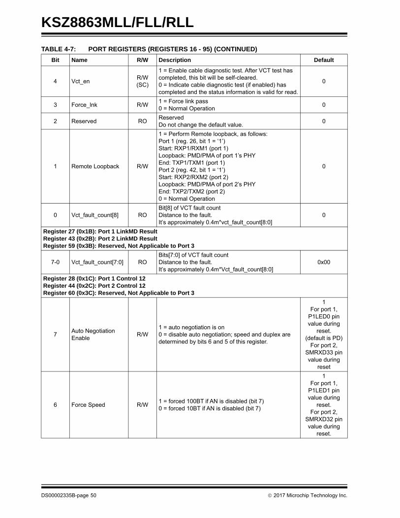
KSZ8863MLL/FLL/RLL
4 Vct_enR/W(SC)
1 = Enable cable diagnostic test. After VCT test has completed, this bit will be self-cleared.0 = Indicate cable diagnostic test (if enabled) has completed and the status information is valid for read.
0
3 Force_lnk R/W1 = Force link pass0 = Normal Operation
0
2 Reserved ROReservedDo not change the default value.
0
1 Remote Loopback R/W
1 = Perform Remote loopback, as follows:Port 1 (reg. 26, bit 1 = ‘1’)Start: RXP1/RXM1 (port 1)Loopback: PMD/PMA of port 1’s PHYEnd: TXP1/TXM1 (port 1)Port 2 (reg. 42, bit 1 = ‘1’)Start: RXP2/RXM2 (port 2)Loopback: PMD/PMA of port 2’s PHYEnd: TXP2/TXM2 (port 2)0 = Normal Operation
0
0 Vct_fault_count[8] ROBit[8] of VCT fault countDistance to the fault. It’s approximately 0.4m*vct_fault_count[8:0]
0
Register 27 (0x1B): Port 1 LinkMD ResultRegister 43 (0x2B): Port 2 LinkMD ResultRegister 59 (0x3B): Reserved, Not Applicable to Port 3
7-0 Vct_fault_count[7:0] ROBits[7:0] of VCT fault countDistance to the fault.It’s approximately 0.4m*Vct_fault_count[8:0]
0x00
Register 28 (0x1C): Port 1 Control 12Register 44 (0x2C): Port 2 Control 12Register 60 (0x3C): Reserved, Not Applicable to Port 3
7Auto Negotiation Enable
R/W1 = auto negotiation is on0 = disable auto negotiation; speed and duplex are determined by bits 6 and 5 of this register.
1For port 1,
P1LED0 pin value during
reset.(default is PD)
For port 2, SMRXD33 pin value during
reset
6 Force Speed R/W1 = forced 100BT if AN is disabled (bit 7)0 = forced 10BT if AN is disabled (bit 7)
1For port 1,
P1LED1 pin value during
reset.For port 2,
SMRXD32 pin value during
reset.
TABLE 4-7: PORT REGISTERS (REGISTERS 16 - 95) (CONTINUED)
Bit Name R/W Description Default
DS00002335B-page 50 2017 Microchip Technology Inc.

KSZ8863MLL/FLL/RLL
5 Force Duplex R/W
1 = forced full-duplex if (1) AN is disabled or (2) AN is enabled but failed.0 = forced half-duplex if (1) AN is disabled or (2) AN is enabled but failed.Note: This bit or strap pin should be set to ‘0’ for the correct duplex mode indication of LED and register status when the link-up is AN to force mode.
1For port 1,
SMRXDV3 pin value during
reset.For port 2,
SMRXD31 pin value during
reset.
4Advertise Flow Control Capability
R/W1 = advertise flow control (pause) capability0 = suppress flow control (pause) capability from transmission to link partner
1
3Advertise 100BT Full-Duplex Capability
R/W1 = advertise 100BT full-duplex capability0 = suppress 100BT full-duplex capability from trans-mission to link partner
1
2Advertise 100BT Half-Duplex Capability
R/W1 = advertise 100BT half-duplex capability0 = suppress 100BT half-duplex capability from trans-mission to link partner
1
1Advertise 10BT Full-Duplex Capability
R/W1 = advertise 10BT full-duplex capability0 = suppress 10BT full-duplex capability from trans-mission to link partner
1
0Advertise 10BT Half-Duplex Capability
R/W1 = advertise 10BT half-duplex capability0 = suppress 10BT half-duplex capability from trans-mission to link partner
1
Register 29 (0x1D): Port 1 Control 13Register 45 (0x2D): Port 2 Control 13Register 61 (0x3D): Reserved, Not Applicable to Port 3
7 LED Off R/W
1 = turn off all port’s LEDs (LEDx_1, LEDx_0, where “x” is the port number). These pins will be driven high if this bit is set to one.0 = normal operation
0
6 Txdis R/W1 = disable the port’s transmitter0 = normal operation
0
5 Restart AN R/W1 = restart auto-negotiation0 = normal operation
0
4Disable Far-End Fault
R/W
1 = disable far-end fault detection and pattern trans-mission.0 = enable far-end fault detection and pattern trans-mission
0
3 Power Down R/W1 = power down0 = normal operation
0
2Disable Auto MDI/MDI-X
R/W1 = disable auto MDI/MDI-X function0 = enable auto MDI/MDI-X function
0
1 Force MDI R/W
If auto MDI/MDI-X is disabled,1 = force PHY into MDI mode (transmit on RXP/RXM pins)0 = force PHY into MDI-X mode (transmit on TXP/TXM pins)
0
TABLE 4-7: PORT REGISTERS (REGISTERS 16 - 95) (CONTINUED)
Bit Name R/W Description Default
2017 Microchip Technology Inc. DS00002335B-page 51

KSZ8863MLL/FLL/RLL
0 Loopback R/W
1 = perform loopback, as indicated:Port 1 Loopback (reg. 29, bit 0 = ‘1’)Start: RXP2/RXM2 (port 2)Loopback: PMD/PMA of port 1’s PHYEnd: TXP2/TXM2 (port 2)Port 2 Loopback (reg. 45, bit 0 = ‘1’)Start: RXP1/RXM1 (port 1)Loopback: PMD/PMA of port 2’s PHYEnd: TXP1/TXM1 (port 1)0 = normal operation
0
Register 30 (0x1E): Port 1 Status 0Register 46 (0x2E): Port 2 Status 0Register 62 (0x3E): Reserved, Not Applicable to Port 3
7 MDI-X Status RO1 = MDI0 = MDI-X
0
6 AN Done RO1 = auto-negotiation completed0 = auto-negotiation not completed
0
5 Link Good RO1 = link good0 = link not good
0
4Partner Flow Con-trol Capability
RO1 = link partner flow control (pause) capable0 = link partner not flow control (pause) capable
0
3Partner 100BT Full-Duplex Capability
RO1 = link partner 100BT full-duplex capable0 = link partner not 100BT full-duplex capable
0
2Partner 100BT Half-Duplex Capability
RO1 = link partner 100BT half-duplex capable0 = link partner not 100BT half-duplex capable
0
1Partner 10BT Full-Duplex Capability
RO1 = link partner 10BT full-duplex capable0 = link partner not 10BT full-duplex capable
0
0Partner 10BT Half-Duplex Capability
RO1 = link partner 10BT half-duplex capable0 = link partner not 10BT half-duplex capable
0
Register 31 (0x1F): Port 1 Status 1Register 47 (0x2F): Port 2 Status 1Register 63 (0x3F): Port 3 Status 1
7 Hp_mdix R/W1 = HP Auto MDI/MDI-X mode0 = Microchip Auto MDI/MDI-X mode
1Note: Only ports 1 and 2 are PHY
ports.This bit is not applicable to port 3 (MII).
6 Reserved ROReservedDo not change the default value.
0
5 Polrvs RO1 = polarity is reversed0 = polarity is not reversed
0Note: This bit is not applicable to
port 3 (MII).This bit is only valid for 10BT
4Transmit Flow Control Enable
RO1 = transmit flow control feature is active0 = transmit flow control feature is inactive
0
3Receive Flow Control Enable
RO1 = receive flow control feature is active0 = receive flow control feature is inactive
0
TABLE 4-7: PORT REGISTERS (REGISTERS 16 - 95) (CONTINUED)
Bit Name R/W Description Default
DS00002335B-page 52 2017 Microchip Technology Inc.
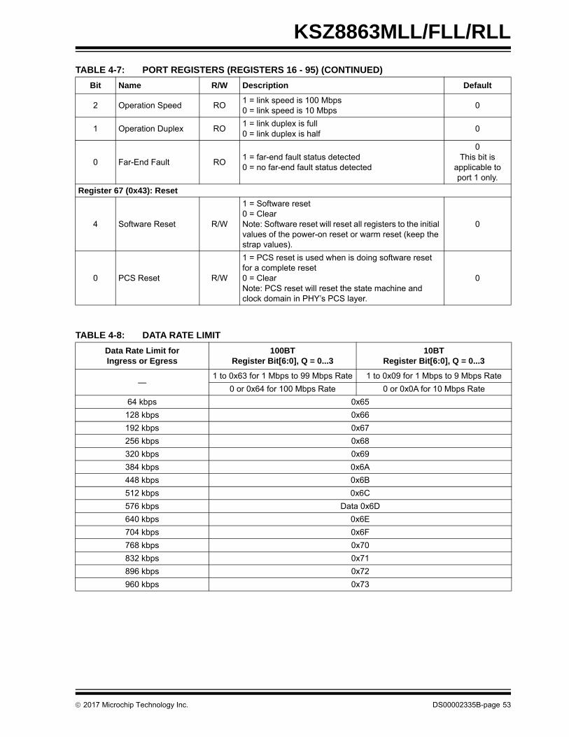
KSZ8863MLL/FLL/RLL
2 Operation Speed RO1 = link speed is 100 Mbps0 = link speed is 10 Mbps
0
1 Operation Duplex RO1 = link duplex is full0 = link duplex is half
0
0 Far-End Fault RO1 = far-end fault status detected0 = no far-end fault status detected
0This bit is
applicable to port 1 only.
Register 67 (0x43): Reset
4 Software Reset R/W
1 = Software reset0 = ClearNote: Software reset will reset all registers to the initial values of the power-on reset or warm reset (keep the strap values).
0
0 PCS Reset R/W
1 = PCS reset is used when is doing software reset for a complete reset0 = ClearNote: PCS reset will reset the state machine and clock domain in PHY’s PCS layer.
0
TABLE 4-8: DATA RATE LIMIT
Data Rate Limit for Ingress or Egress
100BTRegister Bit[6:0], Q = 0...3
10BTRegister Bit[6:0], Q = 0...3
—1 to 0x63 for 1 Mbps to 99 Mbps Rate 1 to 0x09 for 1 Mbps to 9 Mbps Rate
0 or 0x64 for 100 Mbps Rate 0 or 0x0A for 10 Mbps Rate
64 kbps 0x65
128 kbps 0x66
192 kbps 0x67
256 kbps 0x68
320 kbps 0x69
384 kbps 0x6A
448 kbps 0x6B
512 kbps 0x6C
576 kbps Data 0x6D
640 kbps 0x6E
704 kbps 0x6F
768 kbps 0x70
832 kbps 0x71
896 kbps 0x72
960 kbps 0x73
TABLE 4-7: PORT REGISTERS (REGISTERS 16 - 95) (CONTINUED)
Bit Name R/W Description Default
2017 Microchip Technology Inc. DS00002335B-page 53
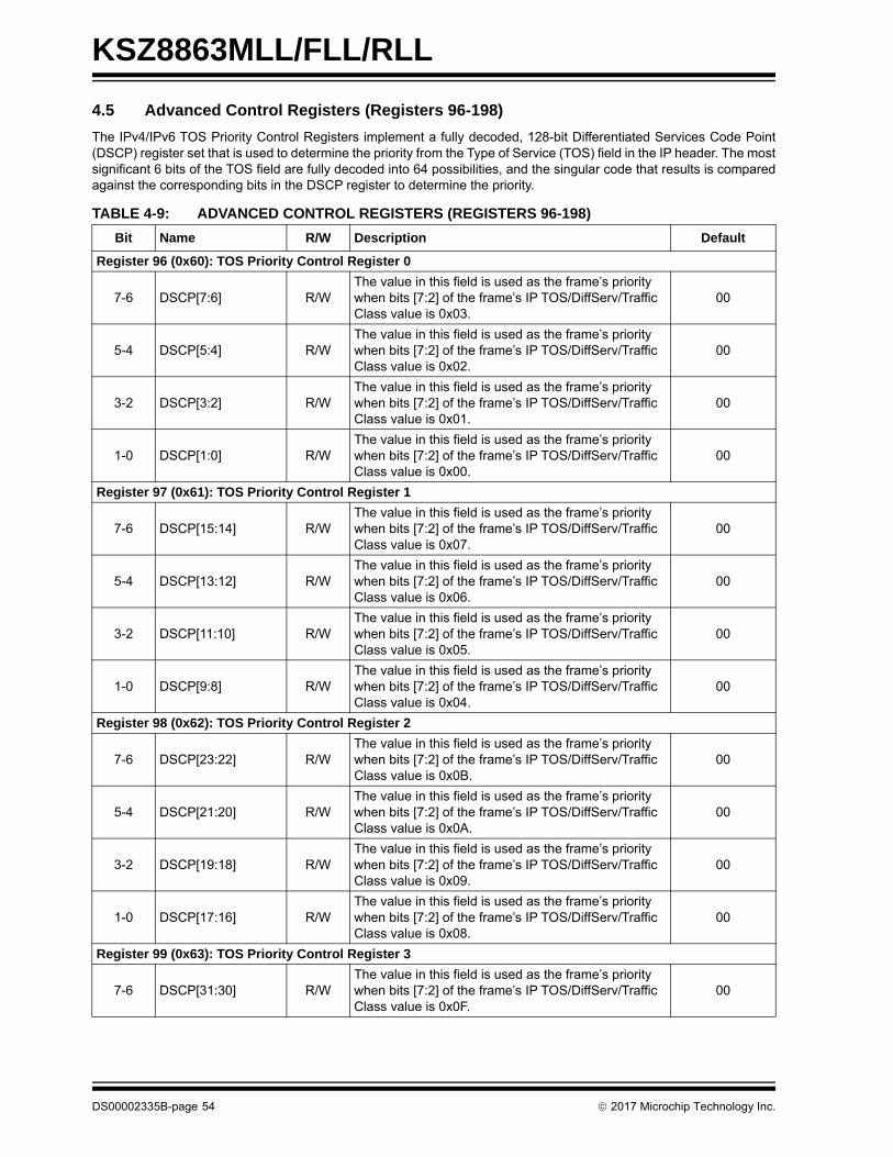
KSZ8863MLL/FLL/RLL
4.5 Advanced Control Registers (Registers 96-198)
The IPv4/IPv6 TOS Priority Control Registers implement a fully decoded, 128-bit Differentiated Services Code Point(DSCP) register set that is used to determine the priority from the Type of Service (TOS) field in the IP header. The mostsignificant 6 bits of the TOS field are fully decoded into 64 possibilities, and the singular code that results is comparedagainst the corresponding bits in the DSCP register to determine the priority.
TABLE 4-9: ADVANCED CONTROL REGISTERS (REGISTERS 96-198)
Bit Name R/W Description Default
Register 96 (0x60): TOS Priority Control Register 0
7-6 DSCP[7:6] R/WThe value in this field is used as the frame’s priority when bits [7:2] of the frame’s IP TOS/DiffServ/Traffic Class value is 0x03.
00
5-4 DSCP[5:4] R/WThe value in this field is used as the frame’s priority when bits [7:2] of the frame’s IP TOS/DiffServ/Traffic Class value is 0x02.
00
3-2 DSCP[3:2] R/WThe value in this field is used as the frame’s priority when bits [7:2] of the frame’s IP TOS/DiffServ/Traffic Class value is 0x01.
00
1-0 DSCP[1:0] R/WThe value in this field is used as the frame’s priority when bits [7:2] of the frame’s IP TOS/DiffServ/Traffic Class value is 0x00.
00
Register 97 (0x61): TOS Priority Control Register 1
7-6 DSCP[15:14] R/WThe value in this field is used as the frame’s priority when bits [7:2] of the frame’s IP TOS/DiffServ/Traffic Class value is 0x07.
00
5-4 DSCP[13:12] R/WThe value in this field is used as the frame’s priority when bits [7:2] of the frame’s IP TOS/DiffServ/Traffic Class value is 0x06.
00
3-2 DSCP[11:10] R/WThe value in this field is used as the frame’s priority when bits [7:2] of the frame’s IP TOS/DiffServ/Traffic Class value is 0x05.
00
1-0 DSCP[9:8] R/WThe value in this field is used as the frame’s priority when bits [7:2] of the frame’s IP TOS/DiffServ/Traffic Class value is 0x04.
00
Register 98 (0x62): TOS Priority Control Register 2
7-6 DSCP[23:22] R/WThe value in this field is used as the frame’s priority when bits [7:2] of the frame’s IP TOS/DiffServ/Traffic Class value is 0x0B.
00
5-4 DSCP[21:20] R/WThe value in this field is used as the frame’s priority when bits [7:2] of the frame’s IP TOS/DiffServ/Traffic Class value is 0x0A.
00
3-2 DSCP[19:18] R/WThe value in this field is used as the frame’s priority when bits [7:2] of the frame’s IP TOS/DiffServ/Traffic Class value is 0x09.
00
1-0 DSCP[17:16] R/WThe value in this field is used as the frame’s priority when bits [7:2] of the frame’s IP TOS/DiffServ/Traffic Class value is 0x08.
00
Register 99 (0x63): TOS Priority Control Register 3
7-6 DSCP[31:30] R/WThe value in this field is used as the frame’s priority when bits [7:2] of the frame’s IP TOS/DiffServ/Traffic Class value is 0x0F.
00
DS00002335B-page 54 2017 Microchip Technology Inc.
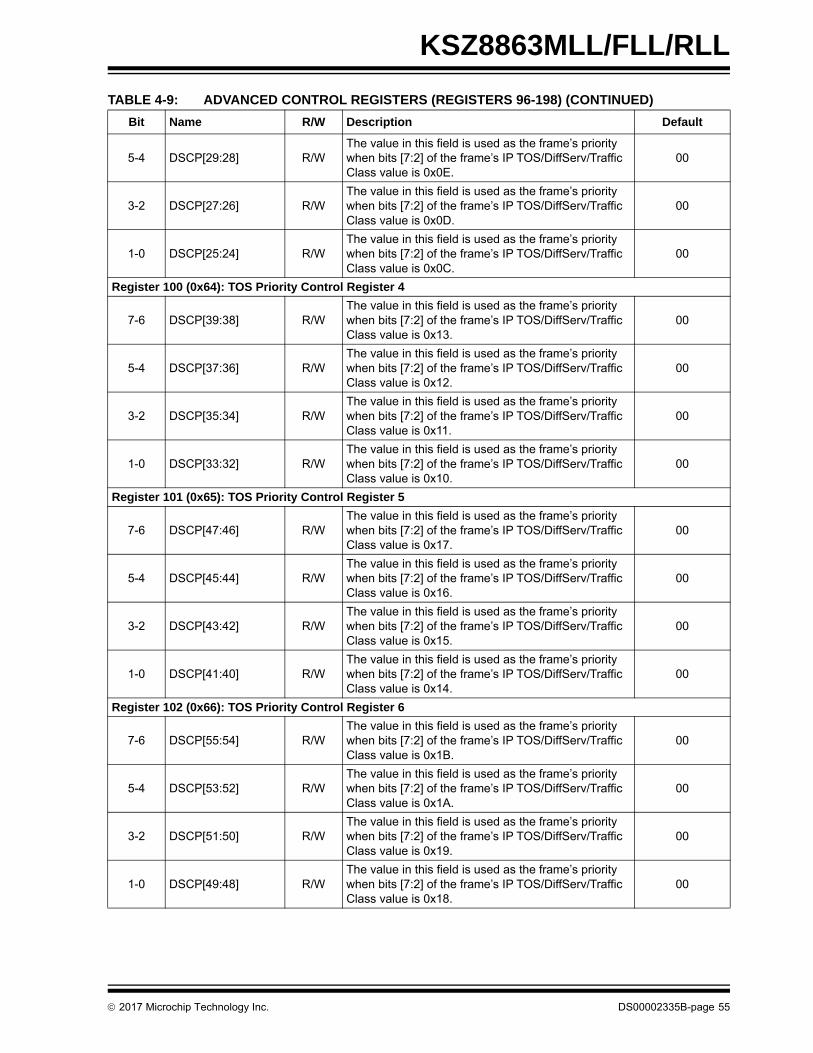
KSZ8863MLL/FLL/RLL
5-4 DSCP[29:28] R/WThe value in this field is used as the frame’s priority when bits [7:2] of the frame’s IP TOS/DiffServ/Traffic Class value is 0x0E.
00
3-2 DSCP[27:26] R/WThe value in this field is used as the frame’s priority when bits [7:2] of the frame’s IP TOS/DiffServ/Traffic Class value is 0x0D.
00
1-0 DSCP[25:24] R/WThe value in this field is used as the frame’s priority when bits [7:2] of the frame’s IP TOS/DiffServ/Traffic Class value is 0x0C.
00
Register 100 (0x64): TOS Priority Control Register 4
7-6 DSCP[39:38] R/WThe value in this field is used as the frame’s priority when bits [7:2] of the frame’s IP TOS/DiffServ/Traffic Class value is 0x13.
00
5-4 DSCP[37:36] R/WThe value in this field is used as the frame’s priority when bits [7:2] of the frame’s IP TOS/DiffServ/Traffic Class value is 0x12.
00
3-2 DSCP[35:34] R/WThe value in this field is used as the frame’s priority when bits [7:2] of the frame’s IP TOS/DiffServ/Traffic Class value is 0x11.
00
1-0 DSCP[33:32] R/WThe value in this field is used as the frame’s priority when bits [7:2] of the frame’s IP TOS/DiffServ/Traffic Class value is 0x10.
00
Register 101 (0x65): TOS Priority Control Register 5
7-6 DSCP[47:46] R/WThe value in this field is used as the frame’s priority when bits [7:2] of the frame’s IP TOS/DiffServ/Traffic Class value is 0x17.
00
5-4 DSCP[45:44] R/WThe value in this field is used as the frame’s priority when bits [7:2] of the frame’s IP TOS/DiffServ/Traffic Class value is 0x16.
00
3-2 DSCP[43:42] R/WThe value in this field is used as the frame’s priority when bits [7:2] of the frame’s IP TOS/DiffServ/Traffic Class value is 0x15.
00
1-0 DSCP[41:40] R/WThe value in this field is used as the frame’s priority when bits [7:2] of the frame’s IP TOS/DiffServ/Traffic Class value is 0x14.
00
Register 102 (0x66): TOS Priority Control Register 6
7-6 DSCP[55:54] R/WThe value in this field is used as the frame’s priority when bits [7:2] of the frame’s IP TOS/DiffServ/Traffic Class value is 0x1B.
00
5-4 DSCP[53:52] R/WThe value in this field is used as the frame’s priority when bits [7:2] of the frame’s IP TOS/DiffServ/Traffic Class value is 0x1A.
00
3-2 DSCP[51:50] R/WThe value in this field is used as the frame’s priority when bits [7:2] of the frame’s IP TOS/DiffServ/Traffic Class value is 0x19.
00
1-0 DSCP[49:48] R/WThe value in this field is used as the frame’s priority when bits [7:2] of the frame’s IP TOS/DiffServ/Traffic Class value is 0x18.
00
TABLE 4-9: ADVANCED CONTROL REGISTERS (REGISTERS 96-198) (CONTINUED)
Bit Name R/W Description Default
2017 Microchip Technology Inc. DS00002335B-page 55
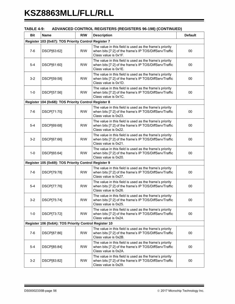
KSZ8863MLL/FLL/RLL
Register 103 (0x67): TOS Priority Control Register 7
7-6 DSCP[63:62] R/WThe value in this field is used as the frame’s priority when bits [7:2] of the frame’s IP TOS/DiffServ/Traffic Class value is 0x1F.
00
5-4 DSCP[61:60] R/WThe value in this field is used as the frame’s priority when bits [7:2] of the frame’s IP TOS/DiffServ/Traffic Class value is 0x1E.
00
3-2 DSCP[59:58] R/WThe value in this field is used as the frame’s priority when bits [7:2] of the frame’s IP TOS/DiffServ/Traffic Class value is 0x1D.
00
1-0 DSCP[57:56] R/WThe value in this field is used as the frame’s priority when bits [7:2] of the frame’s IP TOS/DiffServ/Traffic Class value is 0x1C.
00
Register 104 (0x68): TOS Priority Control Register 8
7-6 DSCP[71:70] R/WThe value in this field is used as the frame’s priority when bits [7:2] of the frame’s IP TOS/DiffServ/Traffic Class value is 0x23.
00
5-4 DSCP[69:68] R/WThe value in this field is used as the frame’s priority when bits [7:2] of the frame’s IP TOS/DiffServ/Traffic Class value is 0x22.
00
3-2 DSCP[67:66] R/WThe value in this field is used as the frame’s priority when bits [7:2] of the frame’s IP TOS/DiffServ/Traffic Class value is 0x21.
00
1-0 DSCP[65:64] R/WThe value in this field is used as the frame’s priority when bits [7:2] of the frame’s IP TOS/DiffServ/Traffic Class value is 0x20.
00
Register 105 (0x69): TOS Priority Control Register 9
7-6 DSCP[79:78] R/WThe value in this field is used as the frame’s priority when bits [7:2] of the frame’s IP TOS/DiffServ/Traffic Class value is 0x27.
00
5-4 DSCP[77:76] R/WThe value in this field is used as the frame’s priority when bits [7:2] of the frame’s IP TOS/DiffServ/Traffic Class value is 0x26.
00
3-2 DSCP[75:74] R/WThe value in this field is used as the frame’s priority when bits [7:2] of the frame’s IP TOS/DiffServ/Traffic Class value is 0x25.
00
1-0 DSCP[73:72] R/WThe value in this field is used as the frame’s priority when bits [7:2] of the frame’s IP TOS/DiffServ/Traffic Class value is 0x24.
00
Register 106 (0x6A): TOS Priority Control Register 10
7-6 DSCP[87:86] R/WThe value in this field is used as the frame’s priority when bits [7:2] of the frame’s IP TOS/DiffServ/Traffic Class value is 0x2B.
00
5-4 DSCP[85:84] R/WThe value in this field is used as the frame’s priority when bits [7:2] of the frame’s IP TOS/DiffServ/Traffic Class value is 0x2A.
00
3-2 DSCP[83:82] R/WThe value in this field is used as the frame’s priority when bits [7:2] of the frame’s IP TOS/DiffServ/Traffic Class value is 0x29.
00
TABLE 4-9: ADVANCED CONTROL REGISTERS (REGISTERS 96-198) (CONTINUED)
Bit Name R/W Description Default
DS00002335B-page 56 2017 Microchip Technology Inc.

KSZ8863MLL/FLL/RLL
1-0 DSCP[81:80] R/WThe value in this field is used as the frame’s priority when bits [7:2] of the frame’s IP TOS/DiffServ/Traffic Class value is 0x28.
00
Register 107 (0x6B): TOS Priority Control Register 11
7-6 DSCP[95:94] R/WThe value in this field is used as the frame’s priority when bits [7:2] of the frame’s IP TOS/DiffServ/Traffic Class value is 0x2F.
00
5-4 DSCP[93:92] R/WThe value in this field is used as the frame’s priority when bits [7:2] of the frame’s IP TOS/DiffServ/Traffic Class value is 0x2E.
00
3-2 DSCP[91:90] R/WThe value in this field is used as the frame’s priority when bits [7:2] of the frame’s IP TOS/DiffServ/Traffic Class value is 0x2D.
00
1-0 DSCP[89:88] R/WThe value in this field is used as the frame’s priority when bits [7:2] of the frame’s IP TOS/DiffServ/Traffic Class value is 0x2C.
00
Register 108 (0x6C): TOS Priority Control Register 12
7-6 DSCP[103:102] R/WThe value in this field is used as the frame’s priority when bits [7:2] of the frame’s IP TOS/DiffServ/Traffic Class value is 0x33.
00
5-4 DSCP[101:100] R/WThe value in this field is used as the frame’s priority when bits [7:2] of the frame’s IP TOS/DiffServ/Traffic Class value is 0x32.
00
3-2 DSCP[99:98] R/WThe value in this field is used as the frame’s priority when bits [7:2] of the frame’s IP TOS/DiffServ/Traffic Class value is 0x31.
00
1-0 DSCP[97:96] R/WThe value in this field is used as the frame’s priority when bits [7:2] of the frame’s IP TOS/DiffServ/Traffic Class value is 0x30.
00
Register 109 (0x6D): TOS Priority Control Register 13
7-6 DSCP[111:110] R/WThe value in this field is used as the frame’s priority when bits [7:2] of the frame’s IP TOS/DiffServ/Traffic Class value is 0x37.
00
5-4 DSCP[109:108] R/WThe value in this field is used as the frame’s priority when bits [7:2] of the frame’s IP TOS/DiffServ/Traffic Class value is 0x36.
00
3-2 DSCP[107:106] R/WThe value in this field is used as the frame’s priority when bits [7:2] of the frame’s IP TOS/DiffServ/Traffic Class value is 0x35.
00
1-0 DSCP[105:104] R/WThe value in this field is used as the frame’s priority when bits [7:2] of the frame’s IP TOS/DiffServ/Traffic Class value is 0x34.
00
Register 110 (0x6E): TOS Priority Control Register 14
7-6 DSCP[119:118] R/WThe value in this field is used as the frame’s priority when bits [7:2] of the frame’s IP TOS/DiffServ/Traffic Class value is 0x3B.
00
5-4 DSCP[117:116] R/WThe value in this field is used as the frame’s priority when bits [7:2] of the frame’s IP TOS/DiffServ/Traffic Class value is 0x3A.
00
TABLE 4-9: ADVANCED CONTROL REGISTERS (REGISTERS 96-198) (CONTINUED)
Bit Name R/W Description Default
2017 Microchip Technology Inc. DS00002335B-page 57

KSZ8863MLL/FLL/RLL
3-2 DSCP[115:114] R/WThe value in this field is used as the frame’s priority when bits [7:2] of the frame’s IP TOS/DiffServ/Traffic Class value is 0x39.
00
1-0 DSCP[113:112] R/WThe value in this field is used as the frame’s priority when bits [7:2] of the frame’s IP TOS/DiffServ/Traffic Class value is 0x38.
00
Register 111 (0x6F): TOS Priority Control Register 15
7-6 DSCP[127:126] R/WThe value in this field is used as the frame’s priority when bits [7:2] of the frame’s IP TOS/DiffServ/Traffic Class value is 0x3F.
00
5-4 DSCP[125:124] R/WThe value in this field is used as the frame’s priority when bits [7:2] of the frame’s IP TOS/DiffServ/Traffic Class value is 0x3E.
00
3-2 DSCP[123:122] R/WThe value in this field is used as the frame’s priority when bits [7:2] of the frame’s IP TOS/DiffServ/Traffic Class value is 0x3D.
00
1-0 DSCP[121:120] R/WThe value in this field is used as the frame’s priority when bits [7:2] of the frame’s IP TOS/DiffServ/Traffic Class value is 0x3C.
00
Registers 112 to 117 contain the switch engine’s MAC address. This 48-bit address is used as the Source Address for the MAC’s full duplex flow control (PAUSE) frame.
Register 112 (0x70): MAC Address Register 0
7-0 MACA[47:40] R/W — 0x00
Register 113 (0x71): MAC Address Register 1
7-0 MACA[39:32] R/W — 0x10
Register 114 (0x72): MAC Address Register 2
7-0 MACA[31:24] R/W — 0xA1
Register 115 (0x73): MAC Address Register 3
7-0 MACA[23:16] R/W — 0xFF
Register 116 (0x74): MAC Address Register 4
7-0 MACA[15:8] R/W — 0xFF
Register 117 (0x75): MAC Address Register 5
7-0 MACA[7:0] R/W — 0xFF
Registers 118 to 120 are User Defined Registers (UDRs). These are general purpose read/write registers that can be used to pass user defined control and status information between the KSZ8863 and the external processor.
Register 118 (0x76): User Defined Register 1
7-0 UDR1 R/W — 0x00
Register 119 (0x77): User Defined Register 2
7-0 UDR2 R/W — 0x00
Register 120 (0x78): User Defined Register 3
7-0 UDR3 R/W — 0x00
Registers 121 to 131 provide read and write access to the static MAC address table, VLAN table, dynamic MAC address table, and MIB counters.
Register 121 (0x79): Indirect Access Control 0
7-5 Reserved R/WReservedDo not change the default values.
000
4Read High/Write Low
R/W1 = read cycle0 = write cycle
0
TABLE 4-9: ADVANCED CONTROL REGISTERS (REGISTERS 96-198) (CONTINUED)
Bit Name R/W Description Default
DS00002335B-page 58 2017 Microchip Technology Inc.
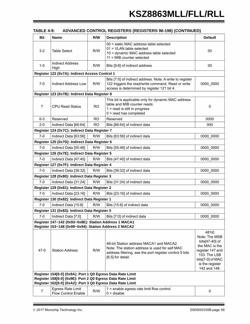
KSZ8863MLL/FLL/RLL
3-2 Table Select R/W
00 = static MAC address table selected01 = VLAN table selected10 = dynamic MAC address table selected11 = MIB counter selected
00
1-0Indirect Address High
R/W Bits [9:8] of indirect address 00
Register 122 (0x7A): Indirect Access Control 1
7-0 Indirect Address Low R/WBits [7:0] of indirect address. Note: A write to register 122 triggers the read/write command. Read or write access is determined by register 121 bit 4.
0000_0000
Register 123 (0x7B): Indirect Data Register 8
7 CPU Read Status RO
This bit is applicable only for dynamic MAC address table and MIB counter reads.1 = read is still in progress0 = read has completed
0
6-3 Reserved RO Reserved 0000
2-0 Indirect Data [66:64] RO Bits [66:64] of indirect data 000
Register 124 (0x7C): Indirect Data Register 7
7-0 Indirect Data [63:56] R/W Bits [63:56] of indirect data 0000_0000
Register 125 (0x7D): Indirect Data Register 6
7-0 Indirect Data [55:48] R/W Bits [55:48] of indirect data 0000_0000
Register 126 (0x7E): Indirect Data Register 5
7-0 Indirect Data [47:40] R/W Bits [47:40] of indirect data 0000_0000
Register 127 (0x7F): Indirect Data Register 4
7-0 Indirect Data [39:32] R/W Bits [39:32] of indirect data 0000_0000
Register 128 (0x80): Indirect Data Register 3
7-0 Indirect Data [31:24] R/W Bits [31:24] of indirect data 0000_0000
Register 129 (0x81): Indirect Data Register 2
7-0 Indirect Data [23:16] R/W Bits [23:16] of indirect data 0000_0000
Register 130 (0x82): Indirect Data Register 1
7-0 Indirect Data [15:8] R/W Bits [15:8] of indirect data 0000_0000
Register 131 (0x83): Indirect Data Register 0
7-0 Indirect Data [7:0] R/W Bits [7:0] of indirect data 0000_0000
Register 147~142 (0x93~0x8E): Station Address 1 MACA1Register 153~148 (0x99~0x94): Station Address 2 MACA2
47-0 Station Address R/W
48-bit Station address MACA1 and MACA2.Note: The station address is used for self MAC address filtering, see the port register control 5 bits [6,5] for detail.
48’h0Note: The MSB bits[47-40] of
the MAC is the register 147 and
153. The LSB bits[7-0] of MAC
is the register 142 and 148.
Register 154[6:0] (0x9A): Port 1 Q0 Egress Data Rate LimitRegister 158[6:0] (0x9E): Port 2 Q0 Egress Data Rate LimitRegister 162[6:0] (0xA2): Port 3 Q0 Egress Data Rate Limit
7Egress Rate Limit Flow Control Enable
R/W1 = enable egress rate limit flow control. 0 = disable
0
TABLE 4-9: ADVANCED CONTROL REGISTERS (REGISTERS 96-198) (CONTINUED)
Bit Name R/W Description Default
2017 Microchip Technology Inc. DS00002335B-page 59
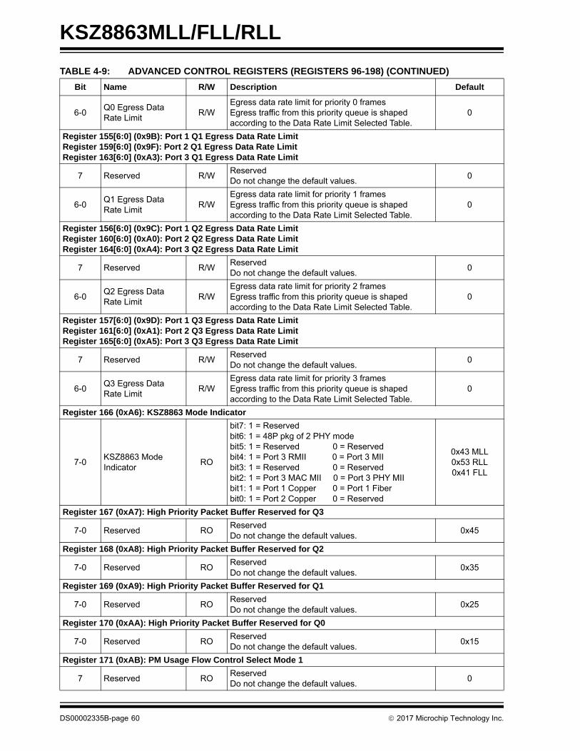
KSZ8863MLL/FLL/RLL
6-0Q0 Egress Data Rate Limit
R/WEgress data rate limit for priority 0 framesEgress traffic from this priority queue is shaped according to the Data Rate Limit Selected Table.
0
Register 155[6:0] (0x9B): Port 1 Q1 Egress Data Rate LimitRegister 159[6:0] (0x9F): Port 2 Q1 Egress Data Rate LimitRegister 163[6:0] (0xA3): Port 3 Q1 Egress Data Rate Limit
7 Reserved R/WReservedDo not change the default values.
0
6-0Q1 Egress Data Rate Limit
R/WEgress data rate limit for priority 1 framesEgress traffic from this priority queue is shaped according to the Data Rate Limit Selected Table.
0
Register 156[6:0] (0x9C): Port 1 Q2 Egress Data Rate LimitRegister 160[6:0] (0xA0): Port 2 Q2 Egress Data Rate LimitRegister 164[6:0] (0xA4): Port 3 Q2 Egress Data Rate Limit
7 Reserved R/WReservedDo not change the default values.
0
6-0Q2 Egress Data Rate Limit
R/WEgress data rate limit for priority 2 framesEgress traffic from this priority queue is shaped according to the Data Rate Limit Selected Table.
0
Register 157[6:0] (0x9D): Port 1 Q3 Egress Data Rate LimitRegister 161[6:0] (0xA1): Port 2 Q3 Egress Data Rate LimitRegister 165[6:0] (0xA5): Port 3 Q3 Egress Data Rate Limit
7 Reserved R/WReservedDo not change the default values.
0
6-0Q3 Egress Data Rate Limit
R/WEgress data rate limit for priority 3 framesEgress traffic from this priority queue is shaped according to the Data Rate Limit Selected Table.
0
Register 166 (0xA6): KSZ8863 Mode Indicator
7-0KSZ8863 Mode Indicator
RO
bit7: 1 = Reserved bit6: 1 = 48P pkg of 2 PHY mode bit5: 1 = Reserved 0 = Reservedbit4: 1 = Port 3 RMII 0 = Port 3 MIIbit3: 1 = Reserved 0 = Reservedbit2: 1 = Port 3 MAC MII 0 = Port 3 PHY MIIbit1: 1 = Port 1 Copper 0 = Port 1 Fiberbit0: 1 = Port 2 Copper 0 = Reserved
0x43 MLL0x53 RLL0x41 FLL
Register 167 (0xA7): High Priority Packet Buffer Reserved for Q3
7-0 Reserved ROReservedDo not change the default values.
0x45
Register 168 (0xA8): High Priority Packet Buffer Reserved for Q2
7-0 Reserved ROReservedDo not change the default values.
0x35
Register 169 (0xA9): High Priority Packet Buffer Reserved for Q1
7-0 Reserved ROReservedDo not change the default values.
0x25
Register 170 (0xAA): High Priority Packet Buffer Reserved for Q0
7-0 Reserved ROReservedDo not change the default values.
0x15
Register 171 (0xAB): PM Usage Flow Control Select Mode 1
7 Reserved ROReservedDo not change the default values.
0
TABLE 4-9: ADVANCED CONTROL REGISTERS (REGISTERS 96-198) (CONTINUED)
Bit Name R/W Description Default
DS00002335B-page 60 2017 Microchip Technology Inc.

KSZ8863MLL/FLL/RLL
6 Reserved ROReservedDo not change the default values.
0
5-0 Reserved ROReservedDo not change the default values.
0x18
Register 172 (0xAC): PM Usage Flow Control Select Mode 2
7-6 Reserved ROReservedDo not change the default values.
0
5-0 Reserved ROReservedDo not change the default values.
0x10
Register 173 (0xAD): PM Usage Flow Control Select Mode 3
7-6 Reserved ROReservedDo not change the default values.
0
5-0 Reserved ROReservedDo not change the default values.
0x08
Register 174 (0xAE): PM Usage Flow Control Select Mode 4
7-4 Reserved ROReservedDo not change the default values.
0
3-0 Reserved ROReservedDo not change the default values.
0x05
Register 175 (0xAF): TXQ Split for Q3 in Port 1
7 Priority Select R/W
0 = enable straight priority with Reg 176/177/178 bits[7]=0 and Reg 5 bit[3]=0 for higher priority first1 = priority ratio is 8:4:2:1 for 4 queues and 2:1 for 2 queues with Reg 176/177/178 bits[7]=1.
1
6-0 Reserved ROReservedDo not change the default values.
8
Register 176 (0xB0): TXQ Split for Q2 in Port 1
7 Priority Select R/W
0 = enable straight priority with Reg 175/177/178 bits[7]=0 and Reg 5 bit[3]=0 for higher priority first1 = priority ratio is 8:4:2:1 for 4 queues and 2:1 for 2 queues with Reg 175/177/178 bits[7]=1.
1
6-0 Reserved ROReservedDo not change the default values.
4
Register 177 (0xB1): TXQ Split for Q1 in Port 1
7 Priority Select R/W
0 = enable straight priority with Reg 175/176/178 bits[7]=0 and Reg 5 bit[3]=0 for higher priority first1 = priority ratio is 8:4:2:1 for 4 queues and 2:1 for 2 queues with Reg 175/176/178 bits[7]=1.
1
6-0 Reserved ROReservedDo not change the default values.
2
Register 178 (0xB2): TXQ Split for Q0 in Port 1
7 Priority Select R/W
0 = enable straight priority with Reg 175/176/177 bits[7]=0 and Reg 5 bit[3]=0 for higher priority first1 = priority ratio is 8:4:2:1 for 4 queues and 2:1 for 2 queues with Reg 175/176/177 bits[7]=1.
1
6-0 Reserved ROReservedDo not change the default values.
1
TABLE 4-9: ADVANCED CONTROL REGISTERS (REGISTERS 96-198) (CONTINUED)
Bit Name R/W Description Default
2017 Microchip Technology Inc. DS00002335B-page 61

KSZ8863MLL/FLL/RLL
Register 179 (0xB3): TXQ Split for Q3 in Port 2
7 Priority Select R/W
0 = enable straight priority with Reg 180/181/182 bits[7]=0 and Reg 5 bit[3]=0 for higher priority first1 = priority ratio is 8:4:2:1 for 4 queues and 2:1 for 2 queues with Reg 180/181/182 bits[7]=1.
1
6-0 Reserved ROReservedDo not change the default values.
8
Register 180 (0xB4): TXQ Split for Q2 in Port 2
7 Priority Select R/W
0 = enable straight priority with Reg 179/181/182 bits[7]=0 and Reg 5 bit[3]=0 for higher priority first1 = priority ratio is 8:4:2:1 for 4 queues and 2:1 for 2 queues with Reg 179/181/182 bits[7]=1.
1
6-0 Reserved ROReservedDo not change the default values.
4
Register 181 (0xB5): TXQ Split for Q1 in Port 2
7 Priority Select R/W
0 = enable straight priority with Reg 179/180/182 bits[7]=0 and Reg 5 bit[3]=0 for higher priority first1 = priority ratio is 8:4:2:1 for 4 queues and 2:1 for 2 queues with Reg 179/180/182 bits[7]=1.
1
6-0 Reserved ROReservedDo not change the default values.
2
Register 182 (0xB6): TXQ Split for Q0 in Port 2
7 Priority Select R/W
0 = enable straight priority with Reg 179/180/181 bits[7]=0 and Reg 5 bit[3]=0 for higher priority first1 = priority ratio is 8:4:2:1 for 4 queues and 2:1 for 2 queues with Reg 179/180/181 bits[7]=1.
1
6-0 Reserved ROReservedDo not change the default values.
1
Register 183 (0xB7): TXQ Split for Q3 Port 3
7 Priority Select R/W
0 = enable straight priority with Reg 184/185/186 bits[7]=0 and Reg 5 bit[3]=0 for higher priority first1 = priority ratio is 8:4:2:1 for 4 queues and 2:1 for 2 queues with Reg 184/185/186 bits[7]=1.
1
6-0 Reserved ROReservedDo not change the default values.
8
Register 184 (0xB8): TXQ Split for Q2 Port 3
7 Priority Select R/W
0 = enable straight priority with Reg 183/185/186 bits[7]=0 and Reg 5 bit[3]=0 for higher priority first1 = priority ratio is 8:4:2:1 for 4 queues and 2:1 for 2 queues with Reg 183/185/186 bits[7]=1.
1
6-0 Reserved ROReservedDo not change the default values.
4
Register 185 (0xB9): TXQ Split for Q1 in Port 3
7 Priority Select R/W
0 = enable straight priority with Reg 183/184/186 bits[7]=0 and Reg 5 bit[3]=0 for higher priority first1 = priority ratio is 8:4:2:1 for 4 queues and 2:1 for 2 queues with Reg 183/184/186 bits[7]=1.
1
6-0 Reserved ROReservedDo not change the default values.
2
TABLE 4-9: ADVANCED CONTROL REGISTERS (REGISTERS 96-198) (CONTINUED)
Bit Name R/W Description Default
DS00002335B-page 62 2017 Microchip Technology Inc.
KSZ8863MLL/FLL/RLL
Register 186 (0xBA): TXQ Split for Q0 in Port 3
7 Priority Select R/W
0 = enable straight priority with Reg 183/184/185 bits[7]=0 and Reg 5 bit[3]=0 for higher priority first1 = priority ratio is 8:4:2:1 for 4 queues and 2:1 for 2 queues with Reg 183/184/185 bits[7]=1.
1
6-0 Reserved ROReservedDo not change the default values.
1
Register 187 (0xBB): Interrupt Enable Register
7-0Interrupt Enable Register
R/W
Interrupt enable register corresponding to bits in Register 188Note: Set register 187 first and then set register 188 (W1C= Write ‘1’ Clear) to wait the interrupt at pin 35 INTRN for the link to be changed.
0x00
Register 188 (0xBC): Link Change Interrupt
7P1 or P2 Link Change (LC) Interrupt
R/WSet to 1 when P1 or P2 link changes in analog inter-face (W1C).
0
6-3 Reserved R/WReservedDo not change the default values.
0
2P3 Link Change (LC) Interrupt
R/W Set to 1 when P3 link changes in MII interface (W1C). 0
1P2 Link Change (LC) Interrupt
R/WSet to 1 when P2 link changes in analog interface (W1C).
0
0P1 MII Link Change (LC) Interrupt
R/WSet to 1 when P1 link changes in analog interface or MII interface (W1C).
0
Register 189 (0xBD): Force Pause Off Iteration Limit Enable
7-0Force Pause Off Iter-ation Limit Enable
R/W1 = Enable. It is 160 ms before requesting to invalidate flow control.0 = Disable
0
Register 192 (0xC0): Fiber Signal Threshold
7Port 2 Fiber Signal Threshold
R/W1 = Threshold is 2.0V0 = Threshold is 1.2V
0
6Port 1 Fiber Signal Threshold
R/W1 = Threshold is 2.0V0 = Threshold is 1.2V
0
5-0 Reserved ROReservedDo not change the default value.
0
Register 193 (0xC1): Internal 1.8V LDO Control
7 Reserved ROReservedDo not change the default value.
0
6Internal 1.8V LDO Disable
R/W1 = Disable internal 1.8V LDO0 = Enable internal 1.8V LDO
0
5-0 Reserved ROReservedDo not change the default value.
0
Register 194 (0xC2): Insert SRC PVID
7-6 Reserved ROReservedDo not change the default value.
00
5Insert SRC Port 1 PVID at Port 2
R/W1= insert SRC port 1 PVID for untagged frame at egress port 2
0
4Insert SRC Port 1 PVID at Port 3
R/W1= insert SRC port 1 PVID for untagged frame at egress port 3
0
TABLE 4-9: ADVANCED CONTROL REGISTERS (REGISTERS 96-198) (CONTINUED)
Bit Name R/W Description Default
2017 Microchip Technology Inc. DS00002335B-page 63
KSZ8863MLL/FLL/RLL
3Insert SRC Port 2 PVID at Port 1
R/W1= insert SRC port 2 PVID for untagged frame at egress port 1
0
2Insert SRC Port 2 PVID at Port 3
R/W1= insert SRC port 2 PVID for untagged frame at egress port 3
0
1Insert SRC Port 3 PVID at Port 1
R/W1= insert SRC port 3 PVID for untagged frame at egress port 1
0
0Insert SRC Port 3 PVID at Port 2
R/W1= insert SRC port 3 PVID for untagged frame at egress port 2
0
Register 195 (0xC3): Power Management and LED Mode
7CPU Interface Power Down
R/W
CPU interface clock tree power down enable.1 = Enable0 = DisableNote: Power save a little bit when MII interface is used and the traffic is stopped in the power management with normal mode
0
6 Switch Power Down R/W
Switch clock tree power down enable.1 = Enable0 = DisableNote: Power save a little bit when MII interface is used and the traffic is stopped in the power management with normal mode
0
5-4 LED Mode Selection R/W
00 = LED0: Link/ACT, LED1: Speed01 = LED0: Link, LED1: ACT10 = LED0: Link/ACT, LED1: Duplex11 = LED0: Link, LED1: Duplex
00
3 LED Output Mode R/W
1 = the internal stretched energy signal from the ana-log module will be negated and output to LED1 and the internal device ready signal will be negated and output to LED0.0 = the LED1/LED0 pins will indicate the regular LED outputs.Note. This is for debugging purpose.
0
2 PLL Off Enable R/W
1 = PLL power down enable0 = disableNote: This bit is used in Energy Detect mode with pin 27 MII_LINK_3 pull-up in the bypass mode for saving power
0
1-0Power Management Mode
R/W
Power management mode00 = Normal Mode 01 = Energy Detection Mode 10 = Software Power Down Mode 11 = Power Saving Mode
00
Register 196(0xC4): Sleep Mode
7-0 Sleep Mode R/W
This value is used to control the minimum period the no energy event has to be detected consecutively before the device enters the low power state when the ED mode is on.The unit is 20 ms. The default go_sleep time is 1.6 seconds.
0x50
Register 198 (0xC6): Forward Invalid VID Frame and Host Mode
7 Reserved ROReservedDo not change the default value.
0
TABLE 4-9: ADVANCED CONTROL REGISTERS (REGISTERS 96-198) (CONTINUED)
Bit Name R/W Description Default
DS00002335B-page 64 2017 Microchip Technology Inc.
KSZ8863MLL/FLL/RLL
4.6 Static MAC Address Table
KSZ8863 supports both a static and a dynamic MAC address table. In response to a Destination Address (DA) look-up,KSZ8863 searches both tables to make a packet forwarding decision. In response to a Source Address (SA) look-up,only the dynamic table is searched for aging, migration, and learning purposes.
The static DA look-up result takes precedence over the dynamic DA look-up result. If there is a DA match in both tables,the result from the static table is used. The entries in the static table will not be aged out by KSZ8863.
The static table is accessed with an external processor via the SMI, SPI, or I2C interfaces. The external processor per-forms all addition, modification, and deletion of static MAC table entries.
Examples:
1. Static Address Table Read (Read the 2nd Entry)
Write to reg. 121 (0x79) with 0x10 // Read static table selected
Write to reg. 122 (0x7A) with 0x01 // Trigger the read operation
Then,
Read reg. 124 (0x7C), static table bits [57:56]
Read reg. 125 (0x7D), static table bits [55:48]
Read reg. 126 (0x7E), static table bits [47:40]
Read reg. 127 (0x7F), static table bits [39:32]
6-4Forward Invid VID Frame
R/W Forwarding ports for frame with invalid VID 3b’0
3P3 RMII Clock Selection
R/W1 = Internal0 = External
0
2P1 RMII Clock Selection
R/W1 = Internal0 = External
0
1-0 Host Interface Mode R/W
00 = I2C master mode01 = I2C slave mode10 = SPI slave mode11 = SMI mode
Strapped value of P2LED1, P2LED0.
TABLE 4-10: FORMAT OF STATIC MAC TABLE (8 ENTRIES)
Bit Name R/W Description Default
57-57 FID R/W Filter VLAN ID – identifies one of the 16 active VLANs 0000
53 Use FID R/W1 = use (FID+MAC) for static table look ups0 = use MAC only for static table look ups
0
52 Override R/W1 = override port setting “transmit enable=0” or “receive enable=0” setting0 = no override
0
51 Valid R/W1 = this entry is valid, the lookup result will be used0 = this entry is not valid
0
50-48 Forwarding Ports R/W
These 3 bits control the forwarding port(s):001, forward to port 1010, forward to port 2100, forward to port 3011, forward to port 1 and port 2110, forward to port 2 and port 3101, forward to port 1 and port 3111, broadcasting (excluding the ingress port)
000
47-0 MAC Address R/W 48-bit MAC Address0x0000_0000
_0000
TABLE 4-9: ADVANCED CONTROL REGISTERS (REGISTERS 96-198) (CONTINUED)
Bit Name R/W Description Default
2017 Microchip Technology Inc. DS00002335B-page 65
KSZ8863MLL/FLL/RLL
Read reg. 128 (0x80), static table bits [31:24]
Read reg. 129 (0x81), static table bits [23:16]
Read reg. 130 (0x82), static table bits [15:8]
Read reg. 131 (0x83), static table bits [7:0]
2. Static Address Table Write (Write the 8th Entry)
Write to reg. 124 (0x7C), static table bits [57:56]
Write to reg. 125 (0x7D), static table bits [55:48]
Write to reg. 126 (0x7E), static table bits [47:40]
Write to reg. 127 (0x7F), static table bits [39:32]
Write to reg. 128 (0x80), static table bits [31:24]
Write to reg. 129 (0x81), static table bits [23:16]
Write to reg. 130 (0x82), static table bits [15:8]
Write to reg. 131 (0x83), static table bits [7:0]
Write to reg. 121 (0x79) with 0x00 // Write static table selected
Write to reg. 122 (0x7A) with 0x07 // Trigger the write operation
4.7 VLAN Table
KSZ8863 uses the VLAN table to perform look-ups. If 802.1Q VLAN mode is enabled (register 5, bit 7 = 1), this table isused to retrieve the VLAN information that is associated with the ingress packet. This information includes FID (filter ID),VID (VLAN ID), and VLAN membership as described in Table 4-11.
If 802.1Q VLAN mode is enabled, KSZ8863 assigns a VID to every ingress packet. If the packet is untagged or taggedwith a null VID, the packet is assigned with the default port VID of the ingress port. If the packet is tagged with a non-null VID, the VID in the tag is used. The look-up process starts from the VLAN table look-up. If the VID is not valid, thepacket are dropped and no address learning takes place. If the VID is valid, the FID is retrieved. The FID+DA andFID+SA look-ups are performed. The FID+DA look-up determines the forwarding ports. If FID+DA fails, the packet isbroadcasted to all the members (excluding the ingress port) of the VLAN. If FID+SA fails, the FID+SA is learned.
Examples:
1. VLAN Table Read (read the 3rd entry)
Write to reg. 121 (0x79) with 0x14 // Read VLAN table selected
Write to reg. 122 (0x7A) with 0x02 // Trigger the read operation
Then,
Read reg. 129 (0x81), VLAN table bits [19:16]
Read reg. 130 (0x82), VLAN table bits [15:8]
TABLE 4-11: FORMAT OF STATIC VLAN TABLE (16 ENTRIES)
Bit Name R/W Description Default
19 Valid R/W1 = entry is valid0 = entry is invalid
1
18-16 Membership R/W
Specify which ports are members of the VLAN. If a DA lookup fails (no match in both static and dynamic tables), the packet associated with this VLAN will be forwarded to ports specified in this field. For example, 101 means port 3 and 1 are in this VLAN.
111
15-12 FID R/W
Filter ID. KSZ8863 supports 16 active VLANs repre-sented by these four bit fields. FID is the mapped ID. If 802.1Q VLAN is enabled, the look up will be based on FID+DA and FID+SA.
0x0
11-0 VID R/W IEEE 802.1Q 12 bits VLAN ID 0x001
DS00002335B-page 66 2017 Microchip Technology Inc.
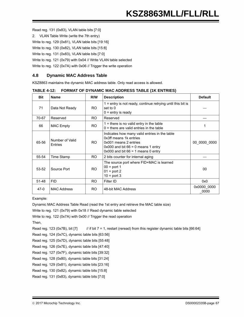
KSZ8863MLL/FLL/RLL
Read reg. 131 (0x83), VLAN table bits [7:0]
2. VLAN Table Write (write the 7th entry)
Write to reg. 129 (0x81), VLAN table bits [19:16]
Write to reg. 130 (0x82), VLAN table bits [15:8]
Write to reg. 131 (0x83), VLAN table bits [7:0]
Write to reg. 121 (0x79) with 0x04 // Write VLAN table selected
Write to reg. 122 (0x7A) with 0x06 // Trigger the write operation
4.8 Dynamic MAC Address Table
KSZ8863 maintains the dynamic MAC address table. Only read access is allowed.
Example:
Dynamic MAC Address Table Read (read the 1st entry and retrieve the MAC table size)
Write to reg. 121 (0x79) with 0x18 // Read dynamic table selected
Write to reg. 122 (0x7A) with 0x00 // Trigger the read operation
Then,
Read reg. 123 (0x7B), bit [7] // if bit 7 = 1, restart (reread) from this register dynamic table bits [66:64]
Read reg. 124 (0x7C), dynamic table bits [63:56]
Read reg. 125 (0x7D), dynamic table bits [55:48]
Read reg. 126 (0x7E), dynamic table bits [47:40]
Read reg. 127 (0x7F), dynamic table bits [39:32]
Read reg. 128 (0x80), dynamic table bits [31:24]
Read reg. 129 (0x81), dynamic table bits [23:16]
Read reg. 130 (0x82), dynamic table bits [15:8]
Read reg. 131 (0x83), dynamic table bits [7:0]
TABLE 4-12: FORMAT OF DYNAMIC MAC ADDRESS TABLE (1K ENTRIES)
Bit Name R/W Description Default
71 Data Not Ready RO1 = entry is not ready, continue retrying until this bit is set to 00 = entry is ready
—
70-67 Reserved RO Reserved —
66 MAC Empty RO1 = there is no valid entry in the table0 = there are valid entries in the table
1
65-56Number of Valid Entries
RO
Indicates how many valid entries in the table0x3ff means 1k entries0x001 means 2 entries0x000 and bit 66 = 0 means 1 entry0x000 and bit 66 = 1 means 0 entry
00_0000_0000
55-54 Time Stamp RO 2 bits counter for internal aging —
53-52 Source Port RO
The source port where FID+MAC is learned00 = port 101 = port 210 = port 3
00
51-48 FID RO Filter ID 0x0
47-0 MAC Address RO 48-bit MAC Address0x0000_0000
_0000
2017 Microchip Technology Inc. DS00002335B-page 67

KSZ8863MLL/FLL/RLL
4.9 Management Information Base (MIB) Counters
KSZ8863 provides 34 MIB counters per port. These counters are used to monitor the port activity for network manage-ment. The MIB counters have two format groups: “Per Port” and “All Port Dropped Packet.”
“Per Port” MIB counters are read using indirect memory access. The base address offsets and address ranges for allthree ports are:
• Port 1, base is 0x00 and range is (0x00-0x1f)
• Port 2, base is 0x20 and range is (0x20-0x3f)
• Port 3, base is 0x40 and range is (0x40-0x5f)
Port 1 MIB counters are read using the indirect memory offsets in Table 4-14.
TABLE 4-13: FORMAT OF “PER PORT” MIB COUNTERS
Bit Name R/W Description Default
31 Overflow RO1 = counter overflow0 = no counter overflow
0
30 Count Valid RO1 = counter value is valid0 = counter value is not valid
0
29-0 Counter Values RO Counter value 0
TABLE 4-14: PORT 1’S “PER PORT” MIB COUNTERS INDIRECT MEMORY OFFSETS
Offset Counter Name Description
0x0 RxLoPriorityByte Rx lo-priority (default) octet count including bad packets
0x1 RxHiPriorityByte Rx hi-priority octet count including bad packets
0x2 RxUndersizePkt Rx undersize packets w/ good CRC
0x3 RxFragments Rx fragment packets w/ bad CRC, symbol errors or alignment errors
0x4 RxOversize Rx oversize packets w/ good CRC (max: 1536 or 1522 bytes)
0x5 RxJabbersRx packets longer than 1522 bytes w/ either CRC errors, alignment errors, or symbol errors (depends on max packet size setting)
0x6 RxSymbolError Rx packets w/ invalid data symbol and legal packet size.
0x7 RxCRCErrorRx packets within (64,1522) bytes w/ an integral number of bytes and a bad CRC (upper limit depends on max packet size setting)
0x8 RxAlignmentErrorRx packets within (64,1522) bytes w/ a non-integral number of bytes and a bad CRC (upper limit depends on max packet size setting)
0x9 RxControl8808PktsNumber of MAC control frames received by a port with 88-08h in Ether-Type field
0xA RxPausePktsNumber of PAUSE frames received by a port. PAUSE frame is qualified with EtherType (88-08h), DA, control opcode (00-01), data length (64B min), and a valid CRC
0xB RxBroadcastRx good broadcast packets (not including error broadcast packets or valid multicast packets)
0xC RxMulticastRx good multicast packets (not including MAC control frames, error multicast packets or valid broadcast packets)
0xD RxUnicast Rx good unicast packets
0xE Rx64Octets Total Rx packets (bad packets included) that were 64 octets in length
0xF Rx65to127OctetsTotal Rx packets (bad packets included) that are between 65 and 127 octets in length
0x10 Rx128to255OctetsTotal Rx packets (bad packets included) that are between 128 and 255 octets in length
0x11 Rx256to511OctetsTotal Rx packets (bad packets included) that are between 256 and 511 octets in length
DS00002335B-page 68 2017 Microchip Technology Inc.
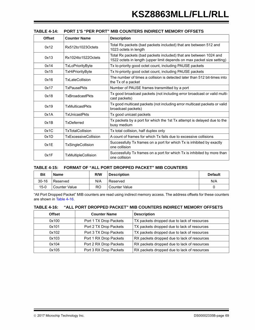
KSZ8863MLL/FLL/RLL
“All Port Dropped Packet” MIB counters are read using indirect memory access. The address offsets for these countersare shown in Table 4-16.
0x12 Rx512to1023OctetsTotal Rx packets (bad packets included) that are between 512 and 1023 octets in length
0x13 Rx1024to1522OctetsTotal Rx packets (bad packets included) that are between 1024 and 1522 octets in length (upper limit depends on max packet size setting)
0x14 TxLoPriorityByte Tx lo-priority good octet count, including PAUSE packets
0x15 TxHiPriorityByte Tx hi-priority good octet count, including PAUSE packets
0x16 TxLateCollisionThe number of times a collision is detected later than 512 bit-times into the Tx of a packet
0x17 TxPausePkts Number of PAUSE frames transmitted by a port
0x18 TxBroadcastPktsTx good broadcast packets (not including error broadcast or valid multi-cast packets)
0x19 TxMulticastPktsTx good multicast packets (not including error multicast packets or valid broadcast packets)
0x1A TxUnicastPkts Tx good unicast packets
0x1B TxDeferredTx packets by a port for which the 1st Tx attempt is delayed due to the busy medium
0x1C TxTotalCollision Tx total collision, half duplex only
0x1D TxExcessiveCollision A count of frames for which Tx fails due to excessive collisions
0x1E TxSingleCollisionSuccessfully Tx frames on a port for which Tx is inhibited by exactly one collision
0x1F TxMultipleCollisionSuccessfully Tx frames on a port for which Tx is inhibited by more than one collision
TABLE 4-15: FORMAT OF “ALL PORT DROPPED PACKET” MIB COUNTERS
Bit Name R/W Description Default
30-16 Reserved N/A Reserved N/A
15-0 Counter Value RO Counter Value 0
TABLE 4-16: “ALL PORT DROPPED PACKET” MIB COUNTERS INDIRECT MEMORY OFFSETS
Offset Counter Name Description
0x100 Port 1 TX Drop Packets TX packets dropped due to lack of resources
0x101 Port 2 TX Drop Packets TX packets dropped due to lack of resources
0x102 Port 3 TX Drop Packets TX packets dropped due to lack of resources
0x103 Port 1 RX Drop Packets RX packets dropped due to lack of resources
0x104 Port 2 RX Drop Packets RX packets dropped due to lack of resources
0x105 Port 3 RX Drop Packets RX packets dropped due to lack of resources
TABLE 4-14: PORT 1’S “PER PORT” MIB COUNTERS INDIRECT MEMORY OFFSETS
Offset Counter Name Description
2017 Microchip Technology Inc. DS00002335B-page 69

KSZ8863MLL/FLL/RLL
Examples:
1. MIB Counter Read (Read port 1 “Rx64Octets” Counter)
Write to reg. 121 (0x79) with 0x1c // Read MIB counters selected
Write to reg. 122 (0x7A) with 0x0e // Trigger the read operation
Then
Read reg. 128 (0x80), overflow bit [31] // If bit 31 = 1, there was a counter overflow
valid bit [30] // If bit 30 = 0, restart (reread) from this register
counter bits [29:24]
Read reg. 129 (0x81), counter bits [23:16]
Read reg. 130 (0x82), counter bits [15:8]
Read reg. 131 (0x83), counter bits [7:0]
2. MIB Counter Read (Read port 2 “Rx64Octets” Counter)
Write to reg. 121 (0x79) with 0x1c // Read MIB counter selected
Write to reg. 122 (0x7A) with 0x2e // Trigger the read operation
Then,
Read reg. 128 (0x80), overflow bit [31] // If bit 31 = 1, there was a counter overflow
valid bit [30] // If bit 30 = 0, restart (reread) from this register
counter bits [29:24]
Read reg. 129 (0x81), counter bits [23:16]
Read reg. 130 (0x82), counter bits [15:8]
Read reg. 131 (0x83), counter bits [7:0]
3. MIB Counter Read (Read “Port1 TX Drop Packets” Counter)
Write to reg. 121 (0x79) with 0x1d // Read MIB counter selected
Write to reg. 122 (0x7A) with 0x00 // Trigger the read operation
Then
Read reg. 130 (0x82), counter bits [15:8]
Read reg. 131 (0x83), counter bits [7:0]
4.9.1 ADDITIONAL MIB COUNTER INFORMATION
“Per Port” MIB counters are designed as “read clear.” These counters are cleared after they are read.
“All Port Dropped Packet” MIB counters are not cleared after they are accessed and do not indicate overflow or validity;therefore, the application must keep track of overflow and valid conditions.
To read out all the counters, the best performance over the SPI bus is (160+3) x 8 x 200 = 260 ms, where there are 160registers, 3 overheads, 8 clocks per access, at 5 MHz. In the heaviest condition, the counters overflow in 2 minutes. Itis recommended that the software reads all the counters at least every 30 seconds.
A high performance SPI master is also recommended to prevent counters overflow.
DS00002335B-page 70 2017 Microchip Technology Inc.

KSZ8863MLL/FLL/RLL
5.0 OPERATIONAL CHARACTERISTICS
5.1 Absolute Maximum Ratings*
Supply Voltage (VIN)(VDDA_1.8, VDDC) ....................................................................................................................................... –0.5V to +2.4V
(VDDA_3.3, VDDIO) ...................................................................................................................................... –0.5V to +4.0V
Input Voltage ............................................................................................................................................. –0.5V to +4.0V
Output Voltage .......................................................................................................................................... –0.5V to +4.0V
Lead Temperature (soldering, 10s) ....................................................................................................................... +260°C
Storage Temperature (TS)...................................................................................................................... –55°C to +150°C
HBM ESD Rating ....................................................................................................................................................... 4 kV
*Exceeding the absolute maximum rating may damage the device. Stresses greater than the absolute maximum ratingmay cause permanent damage to the device. Operation of the device at these or any other conditions above those spec-ified in the operating sections of this specification is not implied. Maximum conditions for extended periods may affectreliability.
5.2 Operating Ratings**
Supply Voltage
(VDDA_1.8, VDDC) ................................................................................................................................... +1.67V to +1.94V
(VDDA_3.3).......................................................................................................................................... +3.135V to +3.465V
(VDDIO) ................................................................................................................................................ +1.71V to +3.465V
Ambient Temperature (TA)
(Commercial)................................................................................................................................................ 0°C to +70°C
(Industrial) ................................................................................................................................................ –40°C to +85°C
Junction Temperature (TJ)..................................................................................................................................... +125°C
Thermal Resistance LQFP (Note 5-1) (ΘJA) ..................................................................................................+52.83°C/W
Thermal Resistance LQFP (Note 5-1) (ΘJC)..................................................................................................+19.12°C/W
**The device is not guaranteed to function outside its operating ratings.
Note 5-1 No heat spreader (HS) in this package.
Note: Do not drive input signals without power supplied to the device.
2017 Microchip Technology Inc. DS00002335B-page 71
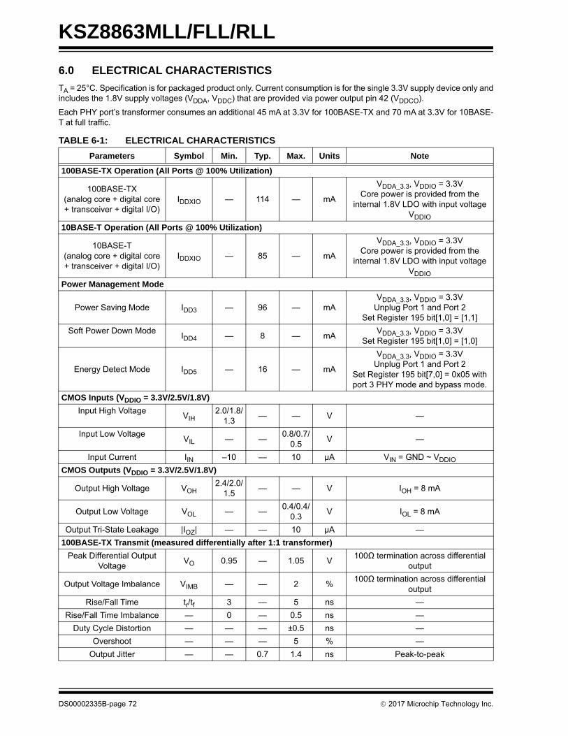
KSZ8863MLL/FLL/RLL
6.0 ELECTRICAL CHARACTERISTICS
TA = 25°C. Specification is for packaged product only. Current consumption is for the single 3.3V supply device only andincludes the 1.8V supply voltages (VDDA, VDDC) that are provided via power output pin 42 (VDDCO).
Each PHY port’s transformer consumes an additional 45 mA at 3.3V for 100BASE-TX and 70 mA at 3.3V for 10BASE-T at full traffic.
TABLE 6-1: ELECTRICAL CHARACTERISTICS
Parameters Symbol Min. Typ. Max. Units Note
100BASE-TX Operation (All Ports @ 100% Utilization)
100BASE-TX (analog core + digital core + transceiver + digital I/O)
IDDXIO — 114 — mA
VDDA_3.3, VDDIO = 3.3VCore power is provided from the
internal 1.8V LDO with input voltage VDDIO
10BASE-T Operation (All Ports @ 100% Utilization)
10BASE-T (analog core + digital core + transceiver + digital I/O)
IDDXIO — 85 — mA
VDDA_3.3, VDDIO = 3.3VCore power is provided from the
internal 1.8V LDO with input voltage VDDIO
Power Management Mode
Power Saving Mode IDD3 — 96 — mAVDDA_3.3, VDDIO = 3.3V
Unplug Port 1 and Port 2Set Register 195 bit[1,0] = [1,1]
Soft Power Down ModeIDD4 — 8 — mA
VDDA_3.3, VDDIO = 3.3VSet Register 195 bit[1,0] = [1,0]
Energy Detect Mode IDD5 — 16 — mA
VDDA_3.3, VDDIO = 3.3VUnplug Port 1 and Port 2
Set Register 195 bit[7,0] = 0x05 with port 3 PHY mode and bypass mode.
CMOS Inputs (VDDIO = 3.3V/2.5V/1.8V)
Input High VoltageVIH
2.0/1.8/1.3
— — V —
Input Low VoltageVIL — —
0.8/0.7/0.5
V —
Input Current IIN –10 — 10 µA VIN = GND ~ VDDIO
CMOS Outputs (VDDIO = 3.3V/2.5V/1.8V)
Output High Voltage VOH2.4/2.0/
1.5— — V IOH = 8 mA
Output Low Voltage VOL — —0.4/0.4/
0.3V IOL = 8 mA
Output Tri-State Leakage |IOZ| — — 10 µA —
100BASE-TX Transmit (measured differentially after 1:1 transformer)
Peak Differential Output Voltage
VO 0.95 — 1.05 V100Ω termination across differential
output
Output Voltage Imbalance VIMB — — 2 %100Ω termination across differential
output
Rise/Fall Time tr/tf 3 — 5 ns —
Rise/Fall Time Imbalance — 0 — 0.5 ns —
Duty Cycle Distortion — — — ±0.5 ns —
Overshoot — — — 5 % —
Output Jitter — — 0.7 1.4 ns Peak-to-peak
DS00002335B-page 72 2017 Microchip Technology Inc.

KSZ8863MLL/FLL/RLL
10BASE-T Receive
Squelch Threshold VSQ — 400 — mV 5 MHz square wave
10BASE-T Transmit (measured differentially after 1:1 transformer)
Peak Differential Output Voltage
VP — 2.4 — V100Ω termination across differential
output
Output Jitter — — 1.4 11 ns Peak-to-peak
TABLE 6-1: ELECTRICAL CHARACTERISTICS (CONTINUED)
Parameters Symbol Min. Typ. Max. Units Note
2017 Microchip Technology Inc. DS00002335B-page 73

KSZ8863MLL/FLL/RLL
7.0 TIMING SPECIFICATIONS
7.1 EEPROM Timing
FIGURE 7-1: EEPROM INTERFACE INPUT TIMING DIAGRAM
FIGURE 7-2: EEPROM INTERFACE OUTPUT TIMING DIAGRAM
TABLE 7-1: EEPROM TIMING PARAMETERS
Symbol Parameter Min. Typ. Max. Units
tcyc1 Clock cycle — 16384 — ns
ts1 Setup time 20 — — ns
th1 Hold time 20 — — ns
tov1 Output valid 4096 4112 4128 ns
SCL
SDA
tcyc1ts1 th1Receive Timing
SCL
SDA
tcyc1Transmit Timing
tov1
DS00002335B-page 74 2017 Microchip Technology Inc.
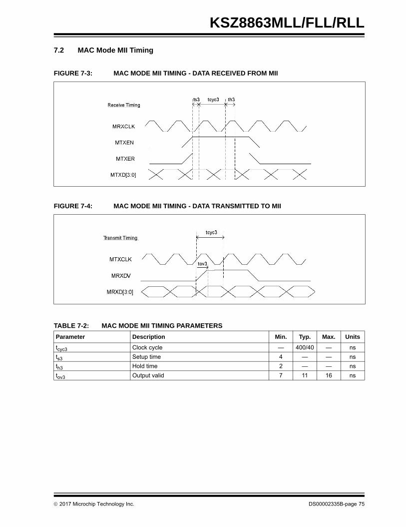
KSZ8863MLL/FLL/RLL
7.2 MAC Mode MII Timing
FIGURE 7-3: MAC MODE MII TIMING - DATA RECEIVED FROM MII
FIGURE 7-4: MAC MODE MII TIMING - DATA TRANSMITTED TO MII
TABLE 7-2: MAC MODE MII TIMING PARAMETERS
Parameter Description Min. Typ. Max. Units
tcyc3 Clock cycle — 400/40 — ns
ts3 Setup time 4 — — ns
th3 Hold time 2 — — ns
tov3 Output valid 7 11 16 ns
2017 Microchip Technology Inc. DS00002335B-page 75

KSZ8863MLL/FLL/RLL
7.3 PHY Mode MII Timing
FIGURE 7-5: PHY MODE MII TIMING - DATA RECEIVED FROM MII
FIGURE 7-6: PHY MODE MII TIMING - DATA TRANSMITTED TO MII
TABLE 7-3: PHY MODE MII TIMING PARAMETERS
Parameter Description Min. Typ. Max. Units
tcyc4 Clock cycle — 400/40 — ns
ts4 Setup time 10 — — ns
th4 Hold time 0 — — ns
tov4 Output valid 18 — 19 ns
DS00002335B-page 76 2017 Microchip Technology Inc.
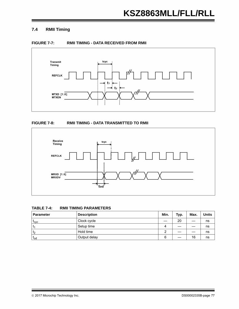
KSZ8863MLL/FLL/RLL
7.4 RMII Timing
FIGURE 7-7: RMII TIMING - DATA RECEIVED FROM RMII
FIGURE 7-8: RMII TIMING - DATA TRANSMITTED TO RMII
TABLE 7-4: RMII TIMING PARAMETERS
Parameter Description Min. Typ. Max. Units
tcyc Clock cycle — 20 — ns
t1 Setup time 4 — — ns
t2 Hold time 2 — — ns
tod Output delay 6 — 16 ns
REFCLK
tcyc
MTXD [1:0]MTXEN
t1
t2
TransmitTiming
REFCLK
tcyc
tod
MRXD [1:0]MRXDV
ReceiveTiming
2017 Microchip Technology Inc. DS00002335B-page 77
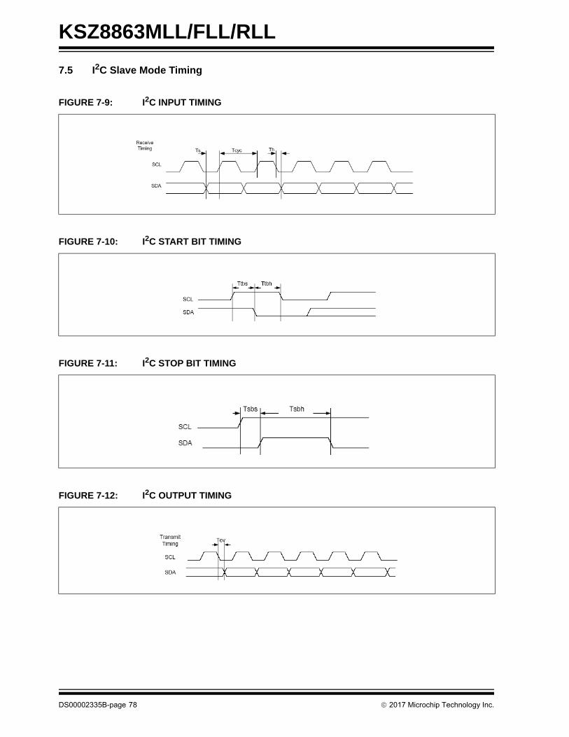
KSZ8863MLL/FLL/RLL
7.5 I2C Slave Mode Timing
FIGURE 7-9: I2C INPUT TIMING
FIGURE 7-10: I2C START BIT TIMING
FIGURE 7-11: I2C STOP BIT TIMING
FIGURE 7-12: I2C OUTPUT TIMING
DS00002335B-page 78 2017 Microchip Technology Inc.

KSZ8863MLL/FLL/RLL
Note that data is only allowed to change during SCL low-time, except the start and stop bits.
TABLE 7-5: I2C TIMING PARAMETERS
Parameter Description Min. Typ. Max. Units
tcyc Clock cycle 400 — — ns
ts Setup time 33 — Half-Cycle
ns
th Hold time 0 — — ns
ttbs Start bit setup time 33 — — ns
ttbh Start bit hold time 33 — — ns
tsbs Stop bit setup time 2 — — ns
tsbh Stop bit hold time 33 — — ns
tov Output valid 64 — 96 ns
2017 Microchip Technology Inc. DS00002335B-page 79
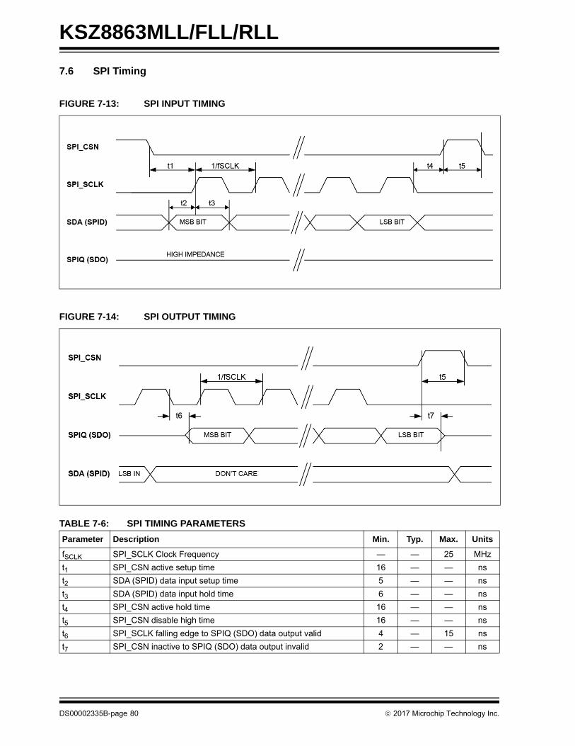
KSZ8863MLL/FLL/RLL
7.6 SPI Timing
FIGURE 7-13: SPI INPUT TIMING
FIGURE 7-14: SPI OUTPUT TIMING
TABLE 7-6: SPI TIMING PARAMETERS
Parameter Description Min. Typ. Max. Units
fSCLK SPI_SCLK Clock Frequency — — 25 MHz
t1 SPI_CSN active setup time 16 — — ns
t2 SDA (SPID) data input setup time 5 — — ns
t3 SDA (SPID) data input hold time 6 — — ns
t4 SPI_CSN active hold time 16 — — ns
t5 SPI_CSN disable high time 16 — — ns
t6 SPI_SCLK falling edge to SPIQ (SDO) data output valid 4 — 15 ns
t7 SPI_CSN inactive to SPIQ (SDO) data output invalid 2 — — ns
DS00002335B-page 80 2017 Microchip Technology Inc.

KSZ8863MLL/FLL/RLL
7.7 Auto-Negotiation Timing
FIGURE 7-15: AUTO-NEGOTIATION TIMING
TABLE 7-7: AUTO-NEGOTIATION TIMING PARAMETERS
Parameter Description Min. Typ. Max. Units
tBTB FLP burst to FLP burst 8 16 24 ms
tFLPW FLP burst width — 2 — ms
tPW Clock/Data pulse width — 100 — ns
tCTD Clock pulse to data pulse 55.5 64 69.5 µs
tCTC Clock pulse to clock pulse 111 128 139 µs
— Number of clock/data pulses per burst 17 — 33 —
Auto-Negotiation - Fast Link Pulse Timing
tPWTX+/TX-
ClockPulse
DataPulse
ClockPulse
tPW
tCTD
tCTC
tFLPW
tBTB
TX+/TX-
DataPulse
FLP Burst
FLP Burst
2017 Microchip Technology Inc. DS00002335B-page 81

KSZ8863MLL/FLL/RLL
7.8 MDC/MDIO Timing
FIGURE 7-16: MDC/MDIO TIMING
TABLE 7-8: MDC/MDIO TIMING PARAMETERS
Parameter Description Min. Typ. Max. Units
tP MDC period — 400 — ns
tMD1 MDIO (PHY Input) setup to rising edge of MDC 10 — — ns
tMD2 MDIO (PHY Input) hold from rising edge of MDC 4 — — ns
tMD3 MDIO (PHY Output) delay from rising edge of MDC — 222 — ns
DS00002335B-page 82 2017 Microchip Technology Inc.

KSZ8863MLL/FLL/RLL
7.9 Reset Timing
The KSZ8863MLL/FLL/RLL reset timing requirement is summarized in Figure 7-17 and Table 7-9.
After the deassertion of reset, wait a minimum of 100 µs before starting programming on the managed interface (I2Cslave, SPI slave, SMI, MIIM).
FIGURE 7-17: RESET TIMING
TABLE 7-9: RESET TIMING PARAMETERS
Parameter Description Min. Typ. Max. Units
tSR Stable supply voltages to reset high 10 — — ms
tCS Configuration setup time 50 — — ns
tCH Configuration hold time 50 — — ns
tRC Reset to strap-in pin output 50 — — ns
tVR 3.3V rise time 100 — — µs
SUPPLYVOLTAGES
RST#
STRAP-INVALUE
STRAP-IN /OUTPUT PIN
tVRtSR
tCS tCH
tRC
2017 Microchip Technology Inc. DS00002335B-page 83

KSZ8863MLL/FLL/RLL
8.0 RESET CIRCUIT
Figure 8-1 shows a reset circuit recommended for powering up the KSZ8863MLL/FLL/RLL if reset is triggered only bythe power supply.
Figure 8-2 shows a reset circuit recommended for applications where reset is driven by another device (for example,the CPU or an FPGA). At power-on-reset, R, C, and D1 provide the necessary ramp rise time to reset the KSZ8863MLL/FLL/RLL device. The RST_OUT_N from the CPU/FPGA provides the warm reset after power-up.
FIGURE 8-1: RECOMMENDED RESET CIRCUIT
FIGURE 8-2: RECOMMENDED RESET CIRCUIT FOR CPU/FPGA RESET OUTPUT
VCC
R10k
C10μF
D1KSZ8863
RST
D1: 1N4148
VCC
R10k
D2C10μF
D1CPU/FPGA
RST_OUT_n
KSZ8863
RST
D1, D2: 1N4148
DS00002335B-page 84 2017 Microchip Technology Inc.

KSZ8863MLL/FLL/RLL
9.0 SELECTION OF ISOLATION TRANSFORMERS
A 1:1 isolation transformer is required at the line interface. Use one with integrated common-mode chokes for designsexceeding FCC requirements.
Table 9-1 lists recommended transformer characteristics.
TABLE 9-1: TRANSFORMER SELECTION CRITERIA
Parameter Value Test Conditions
Turns Ratio 1 CT : 1 CT —
Open-Circuit Inductance (min.) 350 µH 100 mV, 100 kHz, 8 mA
Leakage Inductance (max.) 0.4 µH 1 MHz (min.)
Interwinding Capacitance (max.) 12 pF —
D.C. Resistance (max.) 0.9Ω —
Insertion Loss (max.) –1.0 dB 0 MHz to 65 MHz
HIPOT (min.) 1500 VRMS —
TABLE 9-2: QUALIFIED SINGLE-PORT MAGNETICS
Manufacturer Part Number Auto MDI-X
Bel Fuse S558-5999-U7 Yes
Bel Fuse (MagJack) SI-46001 Yes
Bel Fuse (MagJack) SI-50170 Yes
Delta LF8505 Yes
LanKom LF-H41S Yes
Pulse H1102 Yes
Pulse (Low Cost) H1260 Yes
Datatronic NT79075 Yes
Transpower HB726 Yes
YCL LF-H41S Yes
TDK (MagJack) TLA-6T718 Yes
TABLE 9-3: TYPICAL REFERENCE CRYSTAL CHARACTERISTICS
Characteristic Value
Frequency 25.00000 MHz
Frequency Tolerance (max.) ±50 ppm
Load Capacitance (max.) 20 pF
Series Resistance 40Ω
2017 Microchip Technology Inc. DS00002335B-page 85
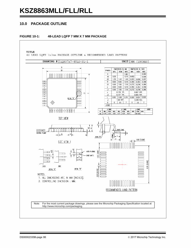
KSZ8863MLL/FLL/RLL
DS00002335B-page 86 2017 Microchip Technology Inc.
10.0 PACKAGE OUTLINE
FIGURE 10-1: 48-LEAD LQFP 7 MM X 7 MM PACKAGE
Note: For the most current package drawings, please see the Microchip Packaging Specification located at http://www.microchip.com/packaging.

2017 Microchip Technology Inc. DS00002335B-page 87
KSZ8863MLL/FLL/RLL
APPENDIX A: DATA SHEET REVISION HISTORY
TABLE A-1: REVISION HISTORY
Revision Section/Figure/Entry Correction
DS00002335A (1-10-17)
—Converted Micrel data sheet KSZ8863MLL/FLL/RLL to Microchip DS00002335A. Minor text changes throughout.
Table 3-5 Updated with a note of RMII interface operation.
Operating Ratings**Update added VDDA_3.3 data.
Updated junction thermal resistance.
DS00002335B (10-19-17)
Table 4-2Changed PHY1 Register 29 (PHYAD = 0x1, REGAD = 0x1D) from “Not support” to “LinkMD Control/Status”.
Table 4-7Changed Register 27 (0x1B) from “Not supported” to “LinkMD Result”.
Figure 7-13 and Figure 7-14Updated the SPI input and output timing illustra-tions.
Table 7-6 Updated the SPI timing parameters.
— Minor text changes throughout.
KSZ8863MLL/FLL/RLL
DS00002335B-page 88 2017 Microchip Technology Inc.
THE MICROCHIP WEB SITE
Microchip provides online support via our WWW site at www.microchip.com. This web site is used as a means to makefiles and information easily available to customers. Accessible by using your favorite Internet browser, the web site con-tains the following information:
• Product Support – Data sheets and errata, application notes and sample programs, design resources, user’s guides and hardware support documents, latest software releases and archived software
• General Technical Support – Frequently Asked Questions (FAQ), technical support requests, online discussion groups, Microchip consultant program member listing
• Business of Microchip – Product selector and ordering guides, latest Microchip press releases, listing of semi-nars and events, listings of Microchip sales offices, distributors and factory representatives
CUSTOMER CHANGE NOTIFICATION SERVICE
Microchip’s customer notification service helps keep customers current on Microchip products. Subscribers will receivee-mail notification whenever there are changes, updates, revisions or errata related to a specified product family ordevelopment tool of interest.
To register, access the Microchip web site at www.microchip.com. Under “Support”, click on “Customer Change Notifi-cation” and follow the registration instructions.
CUSTOMER SUPPORT
Users of Microchip products can receive assistance through several channels:
• Distributor or Representative
• Local Sales Office
• Field Application Engineer (FAE)
• Technical Support
Customers should contact their distributor, representative or field application engineer (FAE) for support. Local salesoffices are also available to help customers. A listing of sales offices and locations is included in the back of this docu-ment.
Technical support is available through the web site at: http://microchip.com/support
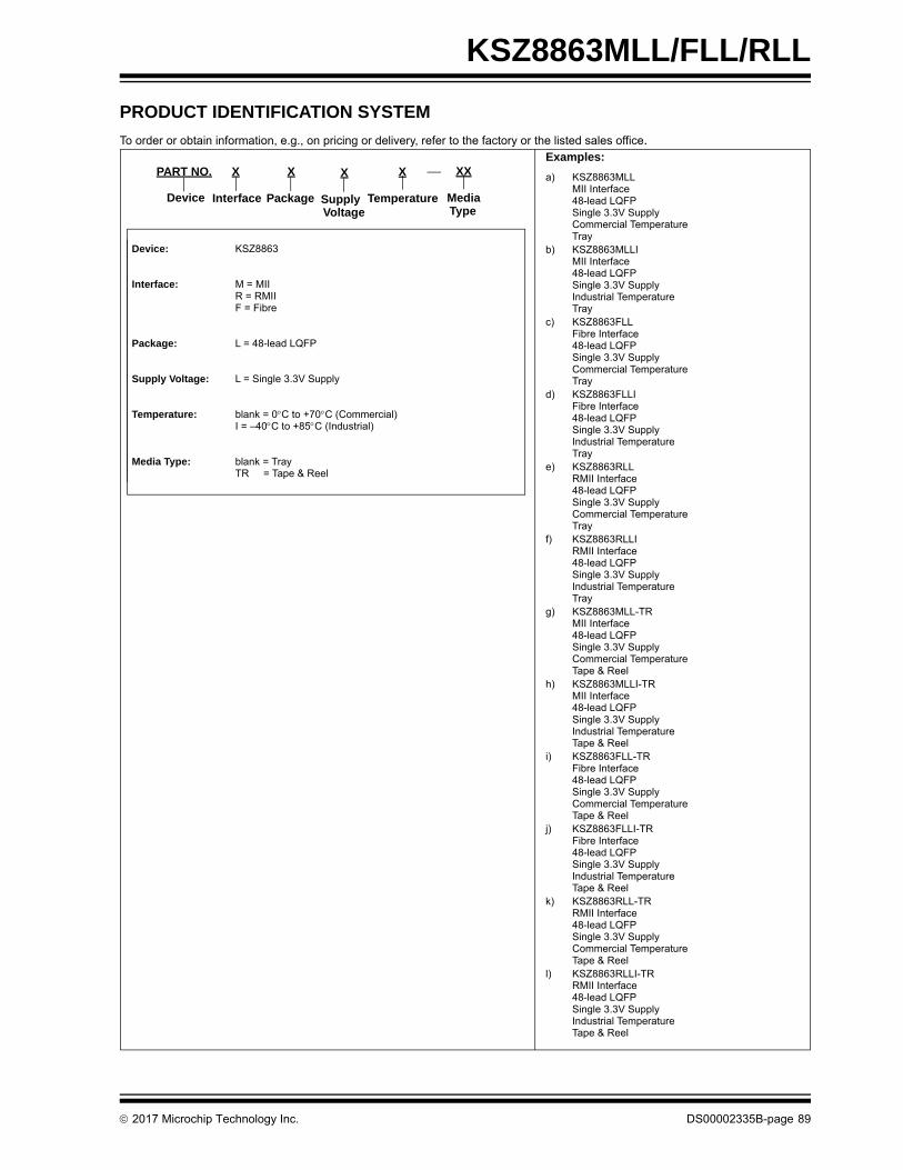
KSZ8863MLL/FLL/RLL
PRODUCT IDENTIFICATION SYSTEM
To order or obtain information, e.g., on pricing or delivery, refer to the factory or the listed sales office.
Device: KSZ8863
Interface: M = MIIR = RMIIF = Fibre
Package: L = 48-lead LQFP
Supply Voltage: L = Single 3.3V Supply
Temperature: blank = 0C to +70C (Commercial)I = –40C to +85C (Industrial)
Media Type: blank = TrayTR = Tape & Reel
Examples:
a) KSZ8863MLLMII Interface48-lead LQFPSingle 3.3V SupplyCommercial TemperatureTray
b) KSZ8863MLLIMII Interface48-lead LQFPSingle 3.3V SupplyIndustrial TemperatureTray
c) KSZ8863FLLFibre Interface48-lead LQFPSingle 3.3V SupplyCommercial TemperatureTray
d) KSZ8863FLLIFibre Interface48-lead LQFPSingle 3.3V SupplyIndustrial TemperatureTray
e) KSZ8863RLLRMII Interface48-lead LQFPSingle 3.3V SupplyCommercial TemperatureTray
f) KSZ8863RLLIRMII Interface48-lead LQFPSingle 3.3V SupplyIndustrial TemperatureTray
g) KSZ8863MLL-TRMII Interface48-lead LQFPSingle 3.3V SupplyCommercial TemperatureTape & Reel
h) KSZ8863MLLI-TRMII Interface48-lead LQFPSingle 3.3V SupplyIndustrial TemperatureTape & Reel
i) KSZ8863FLL-TRFibre Interface48-lead LQFPSingle 3.3V SupplyCommercial TemperatureTape & Reel
j) KSZ8863FLLI-TRFibre Interface48-lead LQFPSingle 3.3V SupplyIndustrial TemperatureTape & Reel
k) KSZ8863RLL-TRRMII Interface48-lead LQFPSingle 3.3V SupplyCommercial TemperatureTape & Reel
l) KSZ8863RLLI-TRRMII Interface48-lead LQFPSingle 3.3V SupplyIndustrial TemperatureTape & Reel
PART NO. X X
PackageInterfaceDevice
X
Temperature
X
SupplyVoltage
XX
MediaType
2017 Microchip Technology Inc. DS00002335B-page 89

KSZ8863MLL/FLL/RLL
NOTES:
DS00002335B-page 90 2017 Microchip Technology Inc.
2017 Microchip Technology Inc. DS00002335B-page 91
Information contained in this publication regarding device applications and the like is provided only for your convenience and may besuperseded by updates. It is your responsibility to ensure that your application meets with your specifications. MICROCHIP MAKES NOREPRESENTATIONS OR WARRANTIES OF ANY KIND WHETHER EXPRESS OR IMPLIED, WRITTEN OR ORAL, STATUTORY OROTHERWISE, RELATED TO THE INFORMATION, INCLUDING BUT NOT LIMITED TO ITS CONDITION, QUALITY, PERFORMANCE,MERCHANTABILITY OR FITNESS FOR PURPOSE. Microchip disclaims all liability arising from this information and its use. Use ofMicrochip devices in life support and/or safety applications is entirely at the buyer’s risk, and the buyer agrees to defend, indemnify andhold harmless Microchip from any and all damages, claims, suits, or expenses resulting from such use. No licenses are conveyed, implic-itly or otherwise, under any Microchip intellectual property rights unless otherwise stated.
Trademarks
The Microchip name and logo, the Microchip logo, AnyRate, AVR, AVR logo, AVR Freaks, BeaconThings, BitCloud, CryptoMemory, CryptoRF, dsPIC, FlashFlex, flexPWR, Heldo, JukeBlox, KEELOQ, KEELOQ logo, Kleer, LANCheck, LINK MD, maXStylus, maXTouch, MediaLB, megaAVR, MOST, MOST logo, MPLAB, OptoLyzer, PIC, picoPower, PICSTART, PIC32 logo, Prochip Designer, QTouch, RightTouch, SAM-BA, SpyNIC, SST, SST Logo, SuperFlash, tinyAVR, UNI/O, and XMEGA are registered trademarks of Microchip Technology Incorporated in the U.S.A. and other countries.
ClockWorks, The Embedded Control Solutions Company, EtherSynch, Hyper Speed Control, HyperLight Load, IntelliMOS, mTouch, Precision Edge, and Quiet-Wire are registered trademarks of Microchip Technology Incorporated in the U.S.A.
Adjacent Key Suppression, AKS, Analog-for-the-Digital Age, Any Capacitor, AnyIn, AnyOut, BodyCom, chipKIT, chipKIT logo, CodeGuard, CryptoAuthentication, CryptoCompanion, CryptoController, dsPICDEM, dsPICDEM.net, Dynamic Average Matching, DAM, ECAN, EtherGREEN, In-Circuit Serial Programming, ICSP, Inter-Chip Connectivity, JitterBlocker, KleerNet, KleerNet logo, Mindi, MiWi, motorBench, MPASM, MPF, MPLAB Certified logo, MPLIB, MPLINK, MultiTRAK, NetDetach, Omniscient Code Generation, PICDEM, PICDEM.net, PICkit, PICtail, PureSilicon, QMatrix, RightTouch logo, REAL ICE, Ripple Blocker, SAM-ICE, Serial Quad I/O, SMART-I.S., SQI, SuperSwitcher, SuperSwitcher II, Total Endurance, TSHARC, USBCheck, VariSense, ViewSpan, WiperLock, Wireless DNA, and ZENA are trademarks of Microchip Technology Incorporated in the U.S.A. and other countries.
SQTP is a service mark of Microchip Technology Incorporated in the U.S.A.
Silicon Storage Technology is a registered trademark of Microchip Technology Inc. in other countries.
GestIC is a registered trademark of Microchip Technology Germany II GmbH & Co. KG, a subsidiary of Microchip Technology Inc., in other countries.
All other trademarks mentioned herein are property of their respective companies.
© 2017, Microchip Technology Incorporated, All Rights Reserved.
ISBN: 978-1-5224-2264-8
Note the following details of the code protection feature on Microchip devices:
• Microchip products meet the specification contained in their particular Microchip Data Sheet.
• Microchip believes that its family of products is one of the most secure families of its kind on the market today, when used in the intended manner and under normal conditions.
• There are dishonest and possibly illegal methods used to breach the code protection feature. All of these methods, to our knowledge, require using the Microchip products in a manner outside the operating specifications contained in Microchip’s Data Sheets. Most likely, the person doing so is engaged in theft of intellectual property.
• Microchip is willing to work with the customer who is concerned about the integrity of their code.
• Neither Microchip nor any other semiconductor manufacturer can guarantee the security of their code. Code protection does not mean that we are guaranteeing the product as “unbreakable.”
Code protection is constantly evolving. We at Microchip are committed to continuously improving the code protection features of ourproducts. Attempts to break Microchip’s code protection feature may be a violation of the Digital Millennium Copyright Act. If such actsallow unauthorized access to your software or other copyrighted work, you may have a right to sue for relief under that Act.
Microchip received ISO/TS-16949:2009 certification for its worldwide headquarters, design and wafer fabrication facilities in Chandler and Tempe, Arizona; Gresham, Oregon and design centers in California and India. The Company’s quality system processes and procedures are for its PIC® MCUs and dsPIC® DSCs, KEELOQ® code hopping devices, Serial EEPROMs, microperipherals, nonvolatile memory and analog products. In addition, Microchip’s quality system for the design and manufacture of development systems is ISO 9001:2000 certified.
QUALITYMANAGEMENTSYSTEMCERTIFIEDBYDNV
== ISO/TS16949==

DS00002335B-page 92 2017 Microchip Technology Inc.
AMERICASCorporate Office2355 West Chandler Blvd.Chandler, AZ 85224-6199Tel: 480-792-7200 Fax: 480-792-7277Technical Support: http://www.microchip.com/supportWeb Address: www.microchip.com
AtlantaDuluth, GA Tel: 678-957-9614 Fax: 678-957-1455
Austin, TXTel: 512-257-3370
BostonWestborough, MA Tel: 774-760-0087 Fax: 774-760-0088
ChicagoItasca, IL Tel: 630-285-0071 Fax: 630-285-0075
DallasAddison, TX Tel: 972-818-7423 Fax: 972-818-2924
DetroitNovi, MI Tel: 248-848-4000
Houston, TX Tel: 281-894-5983
IndianapolisNoblesville, IN Tel: 317-773-8323Fax: 317-773-5453Tel: 317-536-2380
Los AngelesMission Viejo, CA Tel: 949-462-9523Fax: 949-462-9608Tel: 951-273-7800
Raleigh, NC Tel: 919-844-7510
New York, NY Tel: 631-435-6000
San Jose, CA Tel: 408-735-9110Tel: 408-436-4270
Canada - TorontoTel: 905-695-1980 Fax: 905-695-2078
ASIA/PACIFICAsia Pacific OfficeSuites 3707-14, 37th FloorTower 6, The GatewayHarbour City, Kowloon
Hong KongTel: 852-2943-5100Fax: 852-2401-3431
Australia - SydneyTel: 61-2-9868-6733Fax: 61-2-9868-6755
China - BeijingTel: 86-10-8569-7000 Fax: 86-10-8528-2104
China - ChengduTel: 86-28-8665-5511Fax: 86-28-8665-7889
China - ChongqingTel: 86-23-8980-9588Fax: 86-23-8980-9500
China - DongguanTel: 86-769-8702-9880
China - GuangzhouTel: 86-20-8755-8029
China - HangzhouTel: 86-571-8792-8115 Fax: 86-571-8792-8116
China - Hong Kong SARTel: 852-2943-5100 Fax: 852-2401-3431
China - NanjingTel: 86-25-8473-2460Fax: 86-25-8473-2470
China - QingdaoTel: 86-532-8502-7355Fax: 86-532-8502-7205
China - ShanghaiTel: 86-21-3326-8000 Fax: 86-21-3326-8021
China - ShenyangTel: 86-24-2334-2829Fax: 86-24-2334-2393
China - ShenzhenTel: 86-755-8864-2200 Fax: 86-755-8203-1760
China - WuhanTel: 86-27-5980-5300Fax: 86-27-5980-5118
China - XianTel: 86-29-8833-7252Fax: 86-29-8833-7256
ASIA/PACIFICChina - XiamenTel: 86-592-2388138 Fax: 86-592-2388130
China - ZhuhaiTel: 86-756-3210040 Fax: 86-756-3210049
India - BangaloreTel: 91-80-3090-4444 Fax: 91-80-3090-4123
India - New DelhiTel: 91-11-4160-8631Fax: 91-11-4160-8632
India - PuneTel: 91-20-3019-1500
Japan - OsakaTel: 81-6-6152-7160 Fax: 81-6-6152-9310
Japan - TokyoTel: 81-3-6880- 3770 Fax: 81-3-6880-3771
Korea - DaeguTel: 82-53-744-4301Fax: 82-53-744-4302
Korea - SeoulTel: 82-2-554-7200Fax: 82-2-558-5932 or 82-2-558-5934
Malaysia - Kuala LumpurTel: 60-3-6201-9857Fax: 60-3-6201-9859
Malaysia - PenangTel: 60-4-227-8870Fax: 60-4-227-4068
Philippines - ManilaTel: 63-2-634-9065Fax: 63-2-634-9069
SingaporeTel: 65-6334-8870Fax: 65-6334-8850
Taiwan - Hsin ChuTel: 886-3-5778-366Fax: 886-3-5770-955
Taiwan - KaohsiungTel: 886-7-213-7830
Taiwan - TaipeiTel: 886-2-2508-8600 Fax: 886-2-2508-0102
Thailand - BangkokTel: 66-2-694-1351Fax: 66-2-694-1350
EUROPEAustria - WelsTel: 43-7242-2244-39Fax: 43-7242-2244-393
Denmark - CopenhagenTel: 45-4450-2828 Fax: 45-4485-2829
Finland - EspooTel: 358-9-4520-820
France - ParisTel: 33-1-69-53-63-20 Fax: 33-1-69-30-90-79
Germany - GarchingTel: 49-8931-9700Germany - HaanTel: 49-2129-3766400
Germany - HeilbronnTel: 49-7131-67-3636
Germany - KarlsruheTel: 49-721-625370
Germany - MunichTel: 49-89-627-144-0 Fax: 49-89-627-144-44
Germany - RosenheimTel: 49-8031-354-560
Israel - Ra’anana Tel: 972-9-744-7705
Italy - Milan Tel: 39-0331-742611 Fax: 39-0331-466781
Italy - PadovaTel: 39-049-7625286
Netherlands - DrunenTel: 31-416-690399 Fax: 31-416-690340
Norway - TrondheimTel: 47-7289-7561
Poland - WarsawTel: 48-22-3325737
Romania - BucharestTel: 40-21-407-87-50
Spain - MadridTel: 34-91-708-08-90Fax: 34-91-708-08-91
Sweden - GothenbergTel: 46-31-704-60-40
Sweden - StockholmTel: 46-8-5090-4654
UK - WokinghamTel: 44-118-921-5800Fax: 44-118-921-5820
Worldwide Sales and Service
10/10/17