ksb2 manual rev g3 - elecraft manual rev g.pdf · 2 parts inventory the table below lists all parts...
TRANSCRIPT
Elecraft • www.elecraft.com • 831-662-8345
EL E C R A F T KS B2 S S B A D A P T E R
Assembly and Operating Instructions
Revision G, July 2, 2011. Copyright © 2011, Elecraft; All Rights Reserved
Introduction
The KSB2 option provides the Elecraft K2 with single-sideband transceive capability. With the KSB2installed, the operator can use digital communications modes such as RTTY, packet, SSTV and PSK31 inaddition to SSB voice.
The KSB2 includes a 7-pole crystal filter optimized for SSB transmit and receive. This filter is always usedfor SSB transmit. During receive, either the fixed SSB filter or the variable-bandwidth CW crystal filter canbe specified for each of the remaining SSB filter settings (FL2-FL4). The SSB filter can also be used forreceive in CW mode if desired. The BFO is individually programmable for each filter, allowingconsiderable flexibly in optimizing settings for SSB, CW, or digital modes. Transmit and receive BFOsettings can be adjusted independently in SSB modes if desired.
Other features of the KSB2 include a programmable speech compressor and basic VOX (voice-operatedtransmit) capability. In addition, the K2 provides a Carrier Balance mode in which the SSB transmit signalis routed directly to the receiver. This mode facilitates carrier balance adjustment, and can also be used withheadphones to listen to mic audio whenever the mic gain or compression level is changed.
A wide variety of 8-pin microphones can be used with the KSB2. A mic configuration jumper block isprovided on the Front Panel PC board (see Microphone Configuration for details).
This manual supercedes relevant sections of the K2 Owner's Manual.
Specifications
Crystal Filter Bandwidth approx. 2.3 kHz @ -6 dB; 6/60 dB shape factor approx. 2:1Carrier Rejection -40 dB or better (typ)Speech Compressor Compression ratios: 1:1, 2:1, 3:1, 4:1Current Drain 10-15 mASize 4.1 x 2.2 inches (10.4 x 5.6 cm)
i Caution: Some components in this kit can be damaged by static discharge. Beforehandling any transistors or integrated circuits, always put on an anti-static wrist strap or touch anygrounded, unpainted metal surface.
2
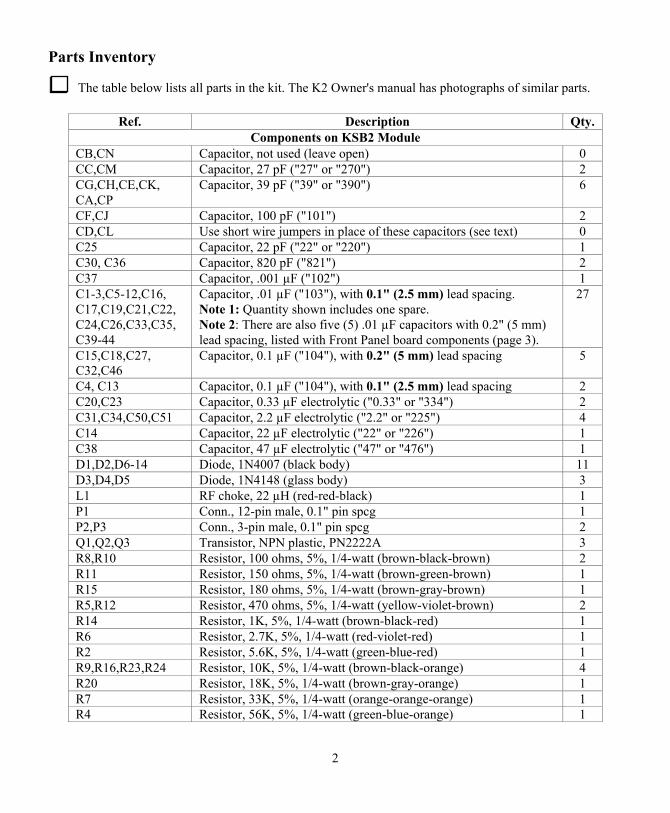
Parts Inventory
The table below lists all parts in the kit. The K2 Owner's manual has photographs of similar parts.
Ref. Description Qty.Components on KSB2 Module
CB,CN Capacitor, not used (leave open) 0CC,CM Capacitor, 27 pF ("27" or "270") 2CG,CH,CE,CK,CA,CP
Capacitor, 39 pF ("39" or "390") 6
CF,CJ Capacitor, 100 pF ("101") 2CD,CL Use short wire jumpers in place of these capacitors (see text) 0C25 Capacitor, 22 pF ("22" or "220") 1C30, C36 Capacitor, 820 pF ("821") 2C37 Capacitor, .001 µF ("102") 1C1-3,C5-12,C16,C17,C19,C21,C22,C24,C26,C33,C35,C39-44
Capacitor, .01 µF ("103"), with 0.1" (2.5 mm) lead spacing.Note 1: Quantity shown includes one spare.Note 2: There are also five (5) .01 µF capacitors with 0.2" (5 mm)lead spacing, listed with Front Panel board components (page 3).
27
C15,C18,C27,C32,C46
Capacitor, 0.1 µF ("104"), with 0.2" (5 mm) lead spacing 5
C4, C13 Capacitor, 0.1 µF ("104"), with 0.1" (2.5 mm) lead spacing 2C20,C23 Capacitor, 0.33 µF electrolytic ("0.33" or "334") 2C31,C34,C50,C51 Capacitor, 2.2 µF electrolytic ("2.2" or "225") 4C14 Capacitor, 22 µF electrolytic ("22" or "226") 1C38 Capacitor, 47 µF electrolytic ("47" or "476") 1D1,D2,D6-14 Diode, 1N4007 (black body) 11D3,D4,D5 Diode, 1N4148 (glass body) 3L1 RF choke, 22 µH (red-red-black) 1P1 Conn., 12-pin male, 0.1" pin spcg 1P2,P3 Conn., 3-pin male, 0.1" pin spcg 2Q1,Q2,Q3 Transistor, NPN plastic, PN2222A 3R8,R10 Resistor, 100 ohms, 5%, 1/4-watt (brown-black-brown) 2R11 Resistor, 150 ohms, 5%, 1/4-watt (brown-green-brown) 1R15 Resistor, 180 ohms, 5%, 1/4-watt (brown-gray-brown) 1R5,R12 Resistor, 470 ohms, 5%, 1/4-watt (yellow-violet-brown) 2R14 Resistor, 1K, 5%, 1/4-watt (brown-black-red) 1R6 Resistor, 2.7K, 5%, 1/4-watt (red-violet-red) 1R2 Resistor, 5.6K, 5%, 1/4-watt (green-blue-red) 1R9,R16,R23,R24 Resistor, 10K, 5%, 1/4-watt (brown-black-orange) 4R20 Resistor, 18K, 5%, 1/4-watt (brown-gray-orange) 1R7 Resistor, 33K, 5%, 1/4-watt (orange-orange-orange) 1R4 Resistor, 56K, 5%, 1/4-watt (green-blue-orange) 1
3
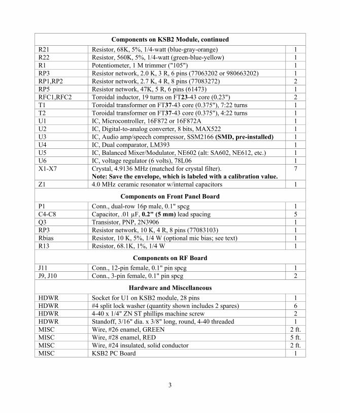
Components on KSB2 Module, continued
R21 Resistor, 68K, 5%, 1/4-watt (blue-gray-orange) 1R22 Resistor, 560K, 5%, 1/4-watt (green-blue-yellow) 1R1 Potentiometer, 1 M trimmer ("105") 1RP3 Resistor network, 2.0 K, 3 R, 6 pins (77063202 or 980663202) 1RP1,RP2 Resistor network, 2.7 K, 4 R, 8 pins (77083272) 2RP5 Resistor network, 47K, 5 R, 6 pins (61473) 1RFC1,RFC2 Toroidal inductor, 19 turns on FT23-43 core (0.23") 2T1 Toroidal transformer on FT37-43 core (0.375"), 7:22 turns 1T2 Toroidal transformer on FT37-43 core (0.375"), 4:22 turns 1U1 IC, Microcontroller, 16F872 or 16F872A 1U2 IC, Digital-to-analog converter, 8 bits, MAX522 1U3 IC, Audio amp/speech compressor, SSM2166 (SMD, pre-installed) 1U4 IC, Dual comparator, LM393 1U5 IC, Balanced Mixer/Modulator, NE602 (alt: SA602, NE612, etc.) 1U6 IC, voltage regulator (6 volts), 78L06 1X1-X7 Crystal, 4.9136 MHz (matched for crystal filter).
Note: Save the envelope, which is labeled with a calibration value.7
Z1 4.0 MHz ceramic resonator w/internal capacitors 1
Components on Front Panel Board
P1 Conn., dual-row 16p male, 0.1" spcg 1C4-C8 Capacitor, .01 µF, 0.2" (5 mm) lead spacing 5Q3 Transistor, PNP, 2N3906 1RP3 Resistor network, 10 K, 4 R, 8 pins (77083103) 1Rbias Resistor, 10 K, 5%, 1/4 W (optional mic bias; see text) 1R13 Resistor, 68.1K, 1%, 1/4 W 1
Components on RF Board
J11 Conn., 12-pin female, 0.1" pin spcg 1J9, J10 Conn., 3-pin female, 0.1" pin spcg 2
Hardware and Miscellaneous
HDWR Socket for U1 on KSB2 module, 28 pins 1HDWR #4 split lock washer (quantity shown includes 2 spares) 6HDWR 4-40 x 1/4" ZN ST phillips machine screw 2HDWR Standoff, 3/16" dia. x 3/8" long, round, 4-40 threaded 1MISC Wire, #26 enamel, GREEN 2 ft.MISC Wire, #28 enamel, RED 5 ft.MISC Wire, #24 insulated, solid conductor 2 ft.MISC KSB2 PC Board 1

4
Firmware Upgrades
If you received new main-processor firmware (U6 on the K2 control board) along with your SSB adapter,you should install and test it before proceeding with assembly. The SSB adapter requires main processorfirmware revision 1.04A or later. (Hold any button on power-up to check your revision number.) Seeseparate instructions that were supplied with the firmware upgrade.
BFO Crystals
If you have a field-test K2 (s/n 1-100), you should have received two replacement BFO crystals. These arerequired to allow proper SSB operation. Install the new BFO crystals and any associated componentsbefore proceeding with KSB2 assembly. See separate instruction sheet.
Assembly Overview
The KSB2 module plugs into the K2 RF board at approximately the location shown below.
RF Board
SSB Adapter
As indicated in the parts list, most of the parts in the kit will be installed on the KSB2 PC board. A smallgroup of parts will be installed on the K2's RF board, and a few on the Front Panel board. The last step inthe assembly process is to wire the microphone connector for your particular mic (P1, Front Panel).

5
The KSB2 PC board uses close-spaced components in the crystal filter area to minimize stray signalpickup. Some capacitors are assigned letters rather than numbers, and some components are not labeled.
Place the KSB2 PC board in front of you as shown below. At the far right end of the board, you'll find anarea with a very symmetrical layout. This area contains the SSB crystal filter and filter switchingcomponents. In the middle of this area are a number of capacitors that are labeled only with letters (A, B,C, D, E, F, G, H, J, K, L, M, N, P). For example, "A" corresponds to capacitor "CA" in the parts list.
Above and below the crystal filter are the filter switching components. Some of the diodes and capacitorsare not labeled on the board itself, but can be identified in the parts placement drawing below.The only other unlabeled components are P2 and P3, which will be installed on the bottom of the board.These are indicated in the upper-right and lower-right corners, below.
All .01 µF capacitors with 0.1" lead spacing use a special symbol with a line between the two pads todistinguish them from small-value capacitors of the same physical size.
U3 (bottom left-hand corner) is a surface-mount device (SMD) and has been pre-installed.
Parts Placement Drawing

6
KSB2 PC Board Assembly
i A fine-point, temperature-controlled soldering iron (700-800 deg. F, 340-370 deg.C) is required to assemble this kit, due to the high density of the PC board layout. A high-wattage iron or one with a wide tip may damage components, pads, or traces. Use aminimum amount of solder to avoid ground shorts.
i To avoid difficulties in soldering adjacent components, install components only inthe order described below. Double-check all values before soldering, since removingsmall parts from double-sided PC boards can be difficult.
Using the parts list (page 3), identify all of the components that are to be installed on the K2's FrontPanel and RF boards and separate them from the remaining items. Note: The .01 µF capacitors with smalllead spacing (0.1", 2.5 mm) are only used on the KSB2 module, while the .01 µF capacitors with the widerlead spacing (0.2", 5 mm) will be installed on the Front Panel board.
Install 12-pin male connector P1 on the bottom of the PC board in the position indicated by itscomponent outline. Do not solder yet. The drawing below shows how P1 should appear viewed from theleft end of the board, with the component side up.
P1 (on bottom)
Component side (top)
Solder just one pin of P1 on the top of the board, near the middle of the connector (pin 6 or 7). Verifythat P1 is now perpendicular to the PC board and is seated completely flat. If not, re-heat the soldered pinand press down on all of P1's pins until the connector drops into place. Once the connector is seatedcorrectly, solder the remaining pins. This connector must not be tilted or installed at the wrong height.
i All component leads should be kept short to avoid stray signal coupling. The leads on smallcapacitors do not need to be straightened, but keep their mounted height at about 1/8" (3 mm) or less.
Install C30 and C36 (820 pF, "821"), near P1 on the top side of the board. Be careful not to confuseC30 or C36 with C18, which is farther from P1 and has wider lead spacing.
Install C25 (22 pF, "22" or "220"), which is near the right end of P1 (viewed from the top side).
7
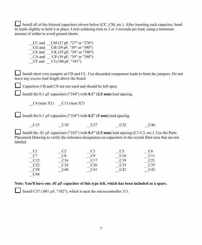
Install all of the lettered capacitors shown below (CC, CM, etc.). After inserting each capacitor, bendits leads slightly to hold it in place. Limit soldering time to 2 or 3 seconds per lead, using a minimumamount of solder to avoid ground shorts.
__CC and __CM (27 pF, "27" or "270")__CG and __CH (39 pF, "39" or "390")__CE and __ CK (39 pF, "39" or "390")__CA and __ CP (39 pF, "39" or "390")__CF and __ CJ (100 pF, "101")
Install short wire jumpers at CD and CL. Use discarded component leads to form the jumpers. Do notleave any excess lead length above the board.
Capacitors CB and CN are not used and should be left open.
Install the 0.1 µF capacitors ("104") with 0.1" (2.5 mm) lead spacing.
__C4 (near X1) __C13 (near X7)
Install the 0.1 µF capacitors ("104") with 0.2" (5 mm) lead spacing.
__C15 __C18 __C27 __C32 __C46
Install the .01 µF capacitors ("103") with 0.1" (2.5 mm) lead spacing (C1-C3, etc.). Use the PartsPlacement Drawing to verify the reference designators on capacitors in the crystal filter area that are notlabeled.
__C1 __C2 __C3 __C5 __C6__C7 __C8 __C9 __C10 __C11__C12 __C16 __C17 __C19 __C21__C22 __C24 __C26 __C33 __C35__C39 __C40 __C41 __C42 __C43__C44
Note: You'll have one .01 µF capacitor of this type left, which has been included as a spare.
Install C37 (.001 µF, "102"), which is near the microcontroller, U1.
8
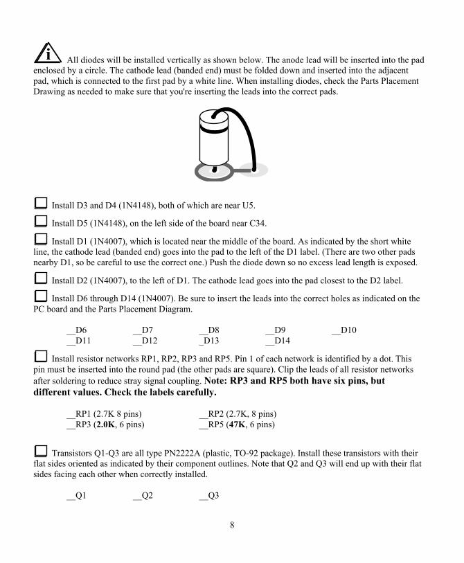
i All diodes will be installed vertically as shown below. The anode lead will be inserted into the padenclosed by a circle. The cathode lead (banded end) must be folded down and inserted into the adjacentpad, which is connected to the first pad by a white line. When installing diodes, check the Parts PlacementDrawing as needed to make sure that you're inserting the leads into the correct pads.
Install D3 and D4 (1N4148), both of which are near U5.
Install D5 (1N4148), on the left side of the board near C34.
Install D1 (1N4007), which is located near the middle of the board. As indicated by the short whiteline, the cathode lead (banded end) goes into the pad to the left of the D1 label. (There are two other padsnearby D1, so be careful to use the correct one.) Push the diode down so no excess lead length is exposed.
Install D2 (1N4007), to the left of D1. The cathode lead goes into the pad closest to the D2 label.
Install D6 through D14 (1N4007). Be sure to insert the leads into the correct holes as indicated on thePC board and the Parts Placement Diagram.
__D6 __D7 __D8 __D9 __D10__D11 __D12 _D13 __D14
Install resistor networks RP1, RP2, RP3 and RP5. Pin 1 of each network is identified by a dot. Thispin must be inserted into the round pad (the other pads are square). Clip the leads of all resistor networksafter soldering to reduce stray signal coupling. Note: RP3 and RP5 both have six pins, butdifferent values. Check the labels carefully.
__RP1 (2.7K 8 pins) __RP2 (2.7K, 8 pins)__RP3 (2.0K, 6 pins) __RP5 (47K, 6 pins)
Transistors Q1-Q3 are all type PN2222A (plastic, TO-92 package). Install these transistors with theirflat sides oriented as indicated by their component outlines. Note that Q2 and Q3 will end up with their flatsides facing each other when correctly installed.
__Q1 __Q2 __Q3

9
U3 is a surface-mount IC that should already be installed on the top side of the board (SSM-2166).Examine U3 with a magnifying glass to verify that all leads are soldered.
Install U6, the 78L06 voltage regulator IC. This device has a plastic package like a transistor. The flatside must face the U6 label as indicated by the component outline.
Install the 28-pin socket for U1. The notched end goes towards the left edge of the board.
Install the 8-pin DIP ICs, U2 through U5. A portion of the part number of each IC is printed on theboard. Compare this number with the number printed on each IC before installation. In all cases, pin 1 ofthe IC (the notched or dimpled end) goes into the round pad (the remaining pads are square).
__U2 (MAX522) __U4 (LM393) __U5 (NE602)
Clip the leads of U5 after soldering to reduce stray coupling. Other IC leads need not be clipped.
Install all of the electrolytic capacitors as indicated by their board outlines. The negative lead isidentified on the case. The positive lead must be inserted into the pad marked "+". The electrolyticcapacitors may all be identical in appearance, so check the values carefully before installation.
__C20 (0.33 µF) __C23 (0.33 µF) __C14 (22 µF) __C31 (2.2 µF)__C34 (2.2 µF) __C38 (47 µF) __C50 (2.2 µF) __C51 (2.2 µF)
Install L1, a solenoidal RF choke, to the right of P1.
The carrier-balance control, R1, is located near the front edge of the board. Press R1 down as far as atwill go, and make sure it is parallel to the board before soldering. Set R1 to its mid-point after soldering.
Install ceramic resonator Z1 near the microcontroller (U1).
Install R5 (470 ohms, yellow-violet-brown), which is located on the far right edge of the board.
Install the remaining resistors on the bottom side of the board. To avoid lead trimming problems, pre-form and trim each resistor's leads before installation. The leads should be just long enough to be visible onthe component side (top). Solder the resistors on the bottom side only. Note: R16's leads will be obscuredby the socket for U1. Trim the leads of R16 so that it sits flat on the bottom of the board.
__R8, __R10 (100 ohms, brown-black-brown)__R11 (150 ohms, brown-green-brown)__R15 (180 ohms, brown-gray-brown)__R12 (470 ohms, yellow-violet-brown)__R14 (1K, brown-black-red)__R6 (2.7K, red-violet-red)__R2 (5.6K, green-blue-red)__R16, __R9 (10K, brown-black-orange; see note on lead trimming above)__R7 (33K, orange-orange-orange)
10
__R4 (56K, green-blue-orange)__R20 (18K, brown-gray-orange)__R21 (68K, blue-gray-orange)__R22 (560K, green-blue-yellow)__R23, __R24 (10K, brown-black-orange)
Re-check the values of capacitors CG and CH (39 pF). Once the crystals are installed (following steps)it is difficult to gain access to these two capacitors.
Locate the envelope containing the matched SSB filter crystals (X1-X7). On the outside of theenvelope you'll find a calibration number that ranges between 3.2 and 3.9. Record the number: ______.Note: If the envelope is unmarked, use 3.6.
Using the number recorded in the previous step, look up the corresponding LSB and USB transmitBFO frequencies in the table below. Record these frequencies in Table 3 (page 20) in the two spacesprovided in the BF1t column.
Xtal Cal # 3.2 3.3 3.4 3.5 3.6 3.7 3.8 3.9LSB 4913.1 4913.2 4913.3 4913.4 4913.5 4913.6 4913.7 4913.8USB 4915.9 4916.0 4916.1 4916.2 4916.3 4916.4 4916.5 4916.6
Install all 7 crystals, making sure that they are flush with the top of the PC board and are not tilted.There should be no excess lead length.
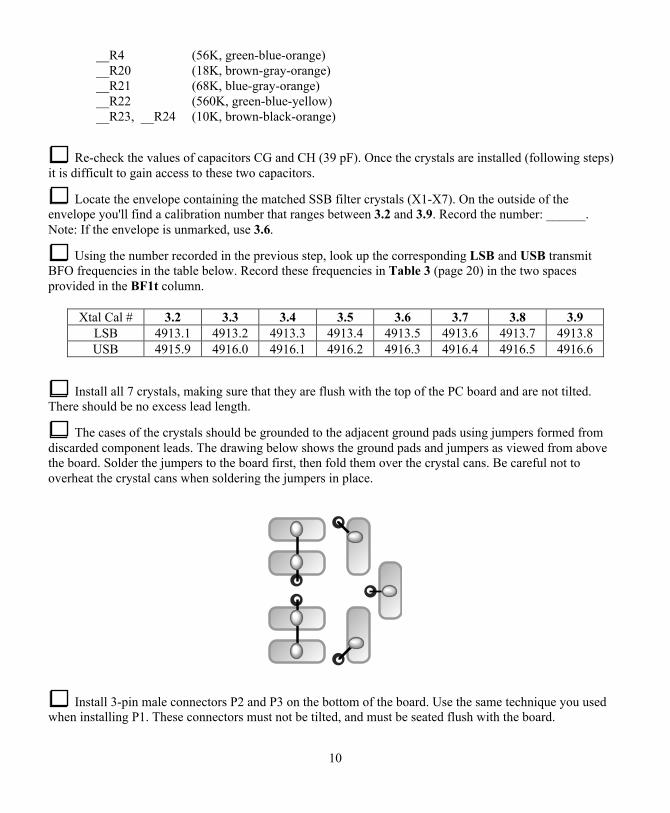
The cases of the crystals should be grounded to the adjacent ground pads using jumpers formed fromdiscarded component leads. The drawing below shows the ground pads and jumpers as viewed from abovethe board. Solder the jumpers to the board first, then fold them over the crystal cans. Be careful not tooverheat the crystal cans when soldering the jumpers in place.
Install 3-pin male connectors P2 and P3 on the bottom of the board. Use the same technique you usedwhen installing P1. These connectors must not be tilted, and must be seated flush with the board.

11
i T1 and T2 are toroidal transformers, with two numbered windings: 1–2 and 3–4. These numbersare printed next to the pads on the PC board, and they also appear on the schematic drawing.
T1 will be wound on a ferrite core (FT37-43, 3/8” [9.5 mm] diameter). For the larger winding, 3-4,use 22 turns of red enamel wire (13”, 33 cm). This winding will occupy about 80 to 90% of the core, asshown in the drawing below. (The drawing shows only 14 turns on the 3-4 winding.) Each pass through thecore counts as one turn. Some turns of the 1-2 winding may cross over those of the 3-4 winding.
Green
4
3
12
Red
Carefully strip and tin the leads of T1’s 3-4 winding as follows: First, cut the leads to about 1/2" (12mm) long. Next, completely remove the enamel insulation from the leads to within 1/8” (3 mm) of the core.You can use a small amount of solder on your iron's tip to heat-strip the insulation (preferred method), oruse a butane lighter or sand-paper. If you scrape the insulation off, be careful not to nick the wire.
T1’s other winding, 1–2, uses 7 turns of green enamel wire (5”, 13 cm). (The drawing shows only 4turns.) Wind the 1–2 winding on top of the 3–4 winding, using about 20% of the core. Strip and tin theleads of the 1–2 winding.
Install T1 vertically as shown by its component outline, with the 1–2 winding facing the edge of theboard. Pull the leads taut on the bottom so that the transformer is held firmly in place. Make sure that theexposed part of each lead is shiny and has no remaining insulation.
Trim and solder all four leads of T1. When soldering, make sure that the solder binds well to theleads. If the lead appears to be an “island” in a small pool of solder, chances are it is not making goodcontact. Measure from leads 1 to 2 and 3 to 4 using an ohmmeter to be sure the leads are making contact.
Wind T2 in the same manner as T1, with 22 turns on the 3-4 winding (red) but only 4 turns on the1–2 winding (green).
Install T2. It will be rotated 180 degrees with respect to T1, with its 1–2 winding (green) facing theclosest edge of the board.

12
i Very small ferrite cores are used for RFC1 and RFC2 to minimize stray signal coupling. Thesecores are a little harder to work with than larger cores, and are also more fragile. If you find it necessary tohold them with a vice, use only plastic or rubber jaws and a minimum of pressure.
Inductor RFC1 is wound with 19 turns of red enamel wire (9" [23 cm]) on an FT23-43 core. Sincethis winding completely fills the core, you may end up with one or two turns overlapping each other on theends, which is acceptable. The edges of the core are sharp, so while winding, try to avoid scraping the wireagainst the core. Prepare the leads as you did with T1 and T2, but leave them long (about 1").
Install RFC1 on the top of the board, even though the component outline appears on the bottom (inthe crystal filter area). The component outline identifies the proper holes to use. Insert the leads into theseholes from the top, then pull the toroid down until it is seated on the board between RP1 and X3. Beforesoldering, look at the leads with a magnifying glass (if necessary) to make sure that all insulation isremoved where the leads intersect the pads. Solder RFC1 on the bottom and clip the excess lead length.
Wind and install RFC2 in the same manner as RFC1.
Use an ohmmeter to verify continuity (< 1 ohm) between the pads for RFC1. Do the same for RFC2.
In the middle of the board, directly above the "C23" label, you'll find two pads connected by a whiteline. Install a 1/4" (6 mm) tall U-shaped ground jumper between these two pads, on the top side of theboard. The jumper can be formed from a discarded component lead. (One of the thick leads from a 1N4007diode is ideal.) This jumper can be used as a ground point for test instruments.
Re-check the orientation of the following using the Parts Placement drawing:
__ ICs __ Resistor Networks __ Diodes__ Transistors __ Electrolytic capacitors
Carefully examine both sides of the board for solder bridges and cold solder joints.
i Before handling microcontroller U1, touch an unpainted, grounded surface. U1 is a CMOS IC thatcan be damaged by static discharge.
Install U1 in its socket. The notched or dimpled end of U1 should be nearest the left edge of theboard. (Pin 1 is indicated by a round pad on the board.)

13
KSB2 Module Installation
Remove the top and bottom covers. (Do not remove the heat sink.)
Disconnect and remove the frequency counter probe.
Locate the 5-crystal CW filter on the K2 RF board (X7 through X11). If any ground wires are solderedto the tops of these crystals, re-locate them to the sides of the crystals, about 1/4" (6 mm) up from thesurface of the PC board. Note: There are two ground pads for each of these crystals (one on either side).For best performance, solder two wires to each crystal. (Early revisions of the K2 manual called for the useof just one wire each, soldered to the tops of the cans, resulting in worse rejection of out-of-band signals.)
Locate the 2nd crystal filter on the RF board (X5 and X6). The ground wires on these two crystalsshould be positioned approximately as shown below to maintain clearance from the SSB adapter.(Grounding of these crystals is non-critical, so either top or side grounding will work.)
Remove jumpers W2 and W3 on the RF board (near the 5-crystal filter). It is best to de-solder thesejumpers and remove them completely rather than just cut them at both ends. If the SSB adapter must beremoved later, W2 and W3 can be re-installed, or you can insert jumpers between pins 1 and 3 of J9/J10.
Desolder and remove C167 from the RF board. C167 is located near the SSB option connector, J11.Save C167 in case you need to remove the SSB adapter at a later date.
Install the 12-pin female connector on the RF board at J11(labeled "SSB") as shown by its outline. Donot solder yet. The side view of J11, below, shows how it should appear once properly seated.
J11
Solder just one pin near the middle of J11. If the connector is not sitting completely flat against the RFboard, reheat this pin and press the connector down. Then solder the remaining pins of J11.
Install 3-pin female connectors on the RF board at J9 and J10, using the same technique used with J11.

14
Install the 3/8" (9.5 mm) standoff on the top of the RF board as shown below, using three split lockwashers and a 1/4" (6 mm) machine screw. The hole for the standoff is near the BFO test point (TP2).
i If you have difficulty getting the screw threads started into the standoff, hold the standoff withpliers on one side while pushing and turning the screw from the other with a phillips screwdriver. Once thelock washers start to compress, the screw will mate adequately with the standoff.
If your K2 serial number is 2999 or lower, you should make the 2nd XFIL modification to the K2 RFboard at this time. This equalizes the pitch of LSB and USB signals on receive, and provides optimalsensitivity in all operating modes. (It has no effect on transmit.) The parts for the modification can bepurchased from Elecraft (part #XFILMDKT ). Instructions can be found in this PDF document:
http://www.elecraft.com/Apps/new_fil_docs/k2_2nd_xfil_ssb_mod.pdf
If you don’t have web access, call or write for a printed copy of the instructions.
Note: The modification has already been incorporated into K2's with serial number 3000 and higher. Youmay also have made this modification already if you upgraded your K2 to revision B.
Plug the SSB module into the RF board. P1 on the SSB module mates with J11 on the RF board, andP2-P3 on the SSB module mate with J9-J10. Note that J11 will be obscured by the SSB adapter as you plugit in, so you won't be able to see whether the pins of P1 are mating correctly. However, if you line up thepins on P2-P3 with J9-J10, the alignment of P1 and J11 should also be correct. Also look at the hole labeled"TP2" on the SSB module: you should see the BFO test point centered below this hole.
Secure the SSB adapter to the RF board standoff using a 4-40 screw and one split lock washer.
Re-install the bottom cover (6 screws).
15
Initial Test
Turn on the K2 and verify that you see the usual ELECRAFT display. If you see INFO 080 or nodisplay, you may have the SSB adapter plugged in incorrectly. If it appears to be installed correctly, unplugthe adapter and look for a short to ground on one of the pins of P1.
Tap the MENU button, then use the BAND + / BAND - buttons to get to the SSBA and SSBCmenu entries. If you see "- -" displayed for SSBA and SSBC , the SSB adapter's microcontroller is notcommunicating with the main processor on the Control board. Make sure U1 on the SSB adapter is notplugged in backwards. Also verify that R12 is installed (470 ohms).
Tap MODE to select CW mode. Set the RF GAIN to max; AF GAIN, mid-way; preamp ON.
Switch to 40 meters using BAND + / BAND - . Connect an antenna and headphones or speaker.
Verify that the K2 performs the same on CW receive as it did prior to installing the SSB adapter. Thefilters you had set up should sound the same, and there should be no loss of signal strength. If signalsappear to be weaker, see Troubleshooting.
BFO Test
Connect the K2's internal frequency counter cable to TP2 (BFO) through the hole labeled "TP2" nearthe center of the SSB module. Tap the MENU button and scroll to the CAL menu entry. Then hold EDITand scroll the CAL parameter until you see CAL FCTR . Hold EDIT a second time to activate thefrequency counter display. You should now see a BFO frequency reading between 4910 and 4918 kHz onthe LCD. The last digit may flicker. If the reading is 0000.00 or out of range, the SSB adapter may beloading down the BFO signal. Check C42, RP3, L1, C25, and C26 on the adapter. Look for shorts or opensin this part of the circuit. Also see Troubleshooting.
Receive-Mode SSB Filter Test
Selecting the Fixed-Bandwidth SSB Filter
If you're still in CAL FCTR mode, tap MENU . Select 40 meters using BAND + / BAND - .
Switch to LSB mode using the MODE button, and use XFIL to select FL1.
Use the menu to select CAL FIL and activate the filter setup display. You'll see filter FL1's settingdisplayed. If a bandwidth number appears after FL1, e.g. FL1 2.20L , it indicates that the variable-bandwidth CW filter is presently being used for SSB receive. The small "L" indicates LSB mode.
Use the VFO knob to change the setting for FL1 to FL1 OP1L . (OP1 is the next available settingafter 2.49 . "OP1" refers to the first option filter, in this case the fixed filter on the SSB adapter.) Youshould hear a pronounced difference in the receiver's audio when you go from 2.49 to OP1 , since thiscauses the SSB adapter to switch between the CW filter and the SSB filter. Leave the filter set forFL1 OP1L . Note: OP2 - OP5 also select OP1 since only one fixed filter is available on the KSB2.

16
BFO Setup for LSB/USB
Tap the BAND - button to see the BFO setting for the first SSB filter (BF1). You should see a displaysimilar to BF1t120L . The BFO frequency control parameter (in this case 120 ) has a range of 000-255.(A lower-case letter t appears in the BFO display for BF1, e.g. BF1t120L . This is a reminder that ontransmit, BFO setting BF1 is always used, regardless of how you set the BFO for FL2 through FL4.)
Tap DISP LAY to show the present LSB BFO frequency in kHz. Adjust the VFO knob until the BFOis as close as possible to the LSB/BF1t freq. from Table 3. Then tap BAND - to return to the BFOparameter display.
Tap MODE to select USB mode. You should now see a display similar to BF1t200U .
Tap DISP LAY to show the present USB BFO frequency in kHz. Adjust the VFO knob until the BFOis as close as possible to the USB/BF1t freq. from Table 3. Tap BAND - .
Exit the menu by tapping MENU .
Using only FL1, listen to a few SSB stations. (Use LSB on 40 meters and below, and USB on 20meters and above.) In later sections we'll describe various ways to set up FL2, 3, and 4 on receive (seeTable 3). You'll also be able to fine-tune the transmit BFO settings, if necessary, to match your voice.Note: Use CAL FIL only on 17 meters and below. The BFO settings for LSB and USB are swapped on 15,12 and 10 meters due to the K2's frequency mixing scheme.
Front Panel Board Components
Remove the two screws that hold the Control board to the Front Panel board. Remove the four chassisscrews that hold the Front Panel assembly to the chassis, then carefully unplug the Front Panel assembly.
Remove the knobs, optical encoder hardware, and the flat-head screw to the left of the encoder shaft.(Do not remove the screw holding the associated standoff to the Front Panel PC board.) Separate the FrontPanel from its PC board.
i The front-panel SSB components will be installed in a small area located between the fourpotentiometers on the left-hand side of the board.
Install the following components on the Front Panel board:
__ C4-C8 (all .01 µF) __ Q3 (2N3906)__ RP3 (10 K, 8 pins) __ R13 (68.1K, 1%)
Turn the Front Panel board upside down and install the microphone configuration connector, P1. Theshort ends of the pins go into the board, and the connector must be soldered on the front side. Be verycareful when soldering the pins of P1, which are very close to pushbutton switch S6.
Re-assemble the Front Panel board (including knobs and hardware), but leave it unplugged.
17
Microphone Configuration
Follow the steps below to configure the K2 for your microphone.
1. If the Front Panel assembly is plugged in, remove the appropriate screws and unplug it. There are twoscrews holding the Front Panel board to the Control board, and four chassis screws that hold the FrontPanel assembly to the chassis.
2. Place the Front Panel board upside-down on a soft cloth, with P1 to your right. P1's left-hand pins arethe K2 signal lines, while those on the right correspond to the 8 pins of the microphone jack.
3. Determine the proper P1 wiring for your mic. First look in Table 2 (following page) to see if your micis listed. (Also check our web site, www.elecraft.com, which lists additional microphones). If you havea mic that is not listed, use Table 1 in conjunction with your microphone's schematic to determinewhich wires to use. If your mic has the wrong connector type, you can use a Radio Shack #274-025.
4. Connect each of the required signal lines using hookup wire, wire-wrap wire, or discarded componentleads. (You can optionally use 2-pin computer "jumper blocks" for connections that tie adjacent P1pins together.) Some mics also require a bias resistor between the AF and 5V lines, as described inTable 1 or Table 2.
5. Plug the Front Panel assembly into the RF board. Secure it to the chassis (4 screws) and control board(2 screws).
Table 1. P1 Signal Descriptions. (Also see Table 2.)
Signal Description NotesAF Mic audio, Low-Z
(approx. 600 ohms).
Approx. 100 mVp-paudio level.
With some mics it is necessary to connect 5V to AFthrough a resistor. The kit includes a 10 K resistor (Rbias)for use with many condenser mics. Some mics may requirea much smaller resistor to supply operating current for abuffer stage. Consult the transceiver and microphoneschematics.
PTT Push-to-talk Contact closure to ground when PTT button pressed.
The PTT signal is the same as the DOT key line, making iteasy to use a foot switch or other method of enabling xmit.
DN "Down" button(optional)
UP "Up" button(optional)
FUNC Function button(optional)
Contact closure to ground when button pressed, otherwiseopen (infinite resistance).
You can activate the VFO A/B switching function usingany contact closure to ground (UP, DN, FUNC). Thepresent version of the KSB2 firmware does not supportother mic button functions.
5V 5 volts DC (10 mAmax.)
Some microphones will work well with 5 volts even thoughthe schematic calls for a higher voltage.
GNDGND
Ground Signal, logic, or shield ground.

18
Table 2. P1 Wiring for Selected Microphones (NC = no connection).
Elecraft MH2, MD2,Proset-K2
Kenwood (MC-43,47,48,60),Alinco EMS-11 Icom (HM-7,12,22,23,36)
Mic kit includes 8 jumper blocksfor use at P1, plus a 5.6-k resistor.Install the jumpers first, then solderthe resistor from pin 1 to 6.Note: Do not attempt dodisassemble the microphone.
Do not connect pin 5 unless michas internal preamp. Touch-toneICs may be sensitive to stray RF.CAUTION: 5V goes to pin 5, notpin 6 (not straight across). Leavepin 6 of the mic unconnected.
Do not connect pin 2 unless michas internal preamp. Touch-toneICs may be sensitive to stray RF.Resistor, AF to 5V: HM-7, 820ohms; HM-12/22/23/36, 10 K
Signal Mic pin Signal Mic pin Signal Mic pinAF 1
(resistor to pin 6)AF 1 AF 1
(see resistor, above)PTT 2 PTT 2 PTT 5DN 3 DN 3 DN 3UP 4 UP 4 UP NC
FUNC 5 FUNC NC FUNC NC5V 6 5V 5 (see note above) 5V 2 (see note above)
GND 7 GND 7 GND 6GND 8 GND 8 GND 7Yaesu (MD-1, MH-1, 27, 31,
YM-35, MD-100)Radio Shack (mic supplied
with HTX-100)
The MD-100 is slightly differentfrom the other mics in the list:connect 5V to pin 2
Signal Mic pin Signal Mic pin Signal Mic pinAF 8 AF 1 AF
PTT 6 PTT 2 PTTDN 3 DN 3 DNUP 1 UP 4 UP
FUNC NC FUNC NC FUNC5V NC (MD-100: pin 2) 5V NC 5V
GND 2 (all but MD-100) GND 7 GNDGND 5, 7 GND 8 GND

19
Alignment
If your K2 serial number is 2999 or lower: Locate the PA Bias control, R60, on the K2's RF boardnear the PA transformer. Set R60 fully counter-clockwise. (Newer K2s have a fixed resistor at R60.)
Locate the carrier balance control, R1 on the KSB2 module. Set it close to the center of its range.
Turn on power to the K2. Select 40 meters, LSB mode, and filter FL1. Set RF GAIN = max.
Coarse Carrier Balance Adjustment
Disconnect the microphone.
Select SSBC in the menu, and set the parameter to 2-1 (2:1 compression).
Select SSBA in the menu, and set the parameter to BAL (carrier balance). Then exit the menu. Youmay see an S-meter indication, since the low-level SSB signal is now being fed back into the receiver.
Adjust R1 on the KSB2 slowly for a minimum indication on the S-meter. This should occur close tothe center of R1's range. If R1 has no effect, see Troubleshooting.
Select SSBA in the menu and set the parameter to 3 . This will disable carrier balance mode.
Fine Carrier Balance Adjustment
A ham-band receiver is required to do fine carrier balance adjustment.
Use the menu to set SSBA to 3 and SSBC to 2-1 .
Connect a microphone to the K2. Select LSB mode and FL1. Set power to 5 watts.
Connect a dummy load to the K2.
Verify that pushing the PTT (push-to-talk) switch on the mic puts the K2 into transmit mode.
Press PTT, but do not talk into the mic. Locate the K2's transmitted signal on the external receiver.The VFO setting you use on the external receiver to listen to your K2's carrier will be different from thatused to tune in the SSB voice signal. If you're tuned to a setting that allows you to hear the voice signal,you'll be at the zero-beat frequency of the carrier and will not be able to hear a tone.
With the PTT switch pressed, adjust R1 on the SSB adapter for minimum carrier signal amplitudeusing the receiver's S-meter. This should occur near the middle of R1's range (typically slightly to theright). Repeat the adjustment using USB. Find the best compromise setting between LSB and USB.

20
Filter Setup
Connect the K2's internal frequency counter probe to TP2 (BFO).
Select 40 meters, LSB mode, and filter FL1. (It's important to always do filter setup on 17 m orbelow to avoid confusion due to the K2's sideband inversion above 17 m. The settings apply to all bands.)
Set up your filters exactly as shown in Table 3 (below), using CAL FIL. Both the filters (FL1-4) andBFOs (BF1-4) must be set up for each operating mode. The BFO settings are given as actual frequencies(4912-4917 kHz) rather than as BFO control values (0-255). As described earlier, the DISP LAY button isused in CAL FIL to setup the BFO frequencies. You may not be able to set the frequencies to exactly thoseshown, but try to get as close as possible. The 10 Hz digit may flicker, which is normal.
Read all of pages 21 and 22 carefully to become familiar with SSB operation.
Set POWER for 5 watts and select LSB mode. Monitor your transmitted voice signal in anotherreceiver, or contact a nearby station and have them listen critically. Then, as explained on page 22 (SSBTransmit BFO Optimization), adjust the LSB BF1 value for best transmitted signal quality.
Switch to USB mode and adjust the USB BF1 value for best transmitted signal quality.
Optional: For receive-mode BFO fine-tuning (BF2-BF4) you can use an audio spectrum analysisprogram such as Spectrogram, which runs on PC-compatible computers. This is described on our web site.
Table 3. Suggested Filter and BFO Settings. (Also see notes below.)
Mode FL1 BF1t (note 1) FL2 BF2 FL3 BF3 FL4 BF4
CW 4913.6 4913.1 4913.1 4913.0
CW Rev.
OP1(note 2) 4916.0
0.70
4914.3
0.40
4914.3
0.20
4914.2
LSB ( _________ )From Page 10
4913.5 4913.0 4912.7
USBOP1
( _________ )From Page 10
OP14916.1
1.804915.5
OFF or0.70
(note 3)
4914.7
Table 3 Notes
1. The LSB and USB BFO settings are derived from the filter crystal frequency (see page 10) to ensuregood SSB transmit performance. The lower-case t after BF1 is a reminder that these BFO settingsare always used on transmit, regardless of which filter you select for receive.
2. FL1 on CW is set for OP1 since the SSB filter is ideal for casual CW tuning. The remaining CWfilters provide narrower bandwidths, and are centered at approximately 600 Hz.
3. FL4 on LSB/USB is shown set to OFF, which means it will not be accessible with the XFIL button.(Any filter can be turned off except for FL1.) To use this filter for PSK-31 or other data modes, setFL4 to 0.70 or narrower. The BF4 settings shown provide a center frequency of about 1000 Hz.

21
Using The SSB Adapter
Basic SSB Setup
Mode Selection: To use SSB, select LSB or USB using the MODE button. Tap AGC to select SLOAGC (recommended for all data modes).
Filter Selection and Setup: Use the XFIL button to select the desired receive-mode crystal filter. In SSBmodes you'll usually select FL2 , since the BFO settings for this filter have been optimized for receive (seeTable 3). In transmit, the BFO settings for FL1 are always used, regardless of what receive filter isselected. This allows you to fine-tune the way your voice sounds on transmit (see SSB Transmit BFOOptimization). For receive purposes, you can set up FL2, 3, and 4 according to Table 3 or modify thesesettings for particular applications. For example, FL4 is shown set to OFF in the table (for SSB modes), butit could be set to any desired bandwidth for voice or data.
Mic Gain: SSBA controls the mic's audio gain. Level 1 attenuates the mic audio by about 10 dB and isuseful when operating outdoors or mobile. (You can change R15 on the SSB adapter if you want a differentattenuation level.) Level 2 turns the mic attenuator off and is the recommended setting for normal indooroperation. Level 3 is similar to level 2 , but provides slightly better VOX sensitivity. BAL is used forcarrier balance adjustment, routing the SSB adapter's output directly to the receiver's I.F. input.
Speech Compressor Level: SSBC controls the speech compressor. 1-1 turns speech compression off.This minimizes audio distortion for digital data modes. 2-1 is the recommended setting for normal voiceoperation. 3-1 and 4-1 may be useful for contest or DX work.
Power/ALC Metering: On power-up, the K2 bargraph LED defaults to RF output metering. To selectALC metering (automatic level control), hold RF/ALC . You'll see ALC flashed on the LCD. In ALCmetering mode, the LEDs illuminate from the right end of the display to distinguish ALC readings from RFpower readings. ALC readings are always shown in BAR mode. (See Power Control and ALC, below.)
Using PTT (SSB and CW modes): On power-up, the K2 defaults to PTT mode. You can also use a footswitch connected to the DOT input (key jack). In CW mode, the mic button can be used as a hand key bysetting INP to HAND in the menu.
Using VOX: Using voice operated transmit (VOX), you can simply talk into the microphone to transmit.To select VOX mode, hold the VOX button. You'll see SPCH 0.2 flashed on the LCD. ("SPCH" means"speech," and "0.2" means an 0.2-second hold time.) Holding the VOX button again selects SPCH 0.4(0.4 second hold time), and holding again selects SPCH 1.0 (1 second). The mode letter flashes slowlyas a reminder that the mic is "live." You'll need to keep the mic away from the K2's speaker, since the K2does not provide "anti-vox" circuitry. This is usually not a problem since the K2's speaker faces upwards.For mobile use or in other high-noise situations, you can set SSBA to 1 to reduce mic gain.
MIC Buttons: Either an UP or DOWN button on your mic can be used to switch between VFOs A and B,assuming you have these lines connected. You'll hear one beep when VFO A is selected, two for VFO B.

22
Power Control and ALC
Tracking ALC: SSB transceivers use Automatic Level Control (ALC) to reduce transmit drive if outputexceeds a desired level. Many transceivers require that you adjust the mic gain manually until the ALCindication is in a certain range. The K2's ALC is different: the drive level is automatically adjusted, overtime, to keep ALC close to the optimal level. This tracking ALC (TALC) eliminates the need to adjust micgain in most cases. You can set the POWER control, mic gain, or speech compression to any level, and theALC level will average between 1 and 3 bars (in ALC meter mode) as you talk.
POWER control: This control is used to set the desired SSB peak power output. The maximum is about10 to 15 watts PEP, depending on the band, antenna impedance, and power supply voltage.1 The minimumpower output in SSB modes is about 1 watt, even if you set the POWER control below this level. (If you setthe POWER level near maximum, the ALC indication will typically be between 0 and 2 bars. Low powersettings (3 watts or less) will result in about 3 bars on average.) Other POWER considerations:
1. Don't set the POWER control any higher than the transmitter is capable of. For example, if youhold TUNE and find that you can only get to 9 watts on 10 meters even with the POWER control allthe way up, you should use POWER settings of 9 watts or less on 10 meters, in all modes.
2. Use lower power when using a battery. Don't use > 10 watts unless you're running from 13-15V.3. Set CAL CUR to no more than 3.5 amps. This will allow the K2 to remind you when the PA
transistors are drawing too much current, so you can reduce power before they get too warm. If yousee a HI CUR warning message, reduce power until the warning goes away.
4. If you get a mic burn or a report that your signal is distorted: This is usually an indication that youhave high RF voltage on the K2 chassis due to the use of an end-fed or poorly-matched antenna. Theproblem can be solved by using an RF Isolator, available from Elecraft and other manufactures.
5. Use 5 watts or less for digital data modes, since the duty cycle for digital modes can approach 100%.Use 1:1 or 2:1 speech compression for minimum data distortion (SSBC 1-1 or 2-1 ).
SSB Transmit BFO Optimization (Important)
When you transmit using SSB mode, the fixed filter on the SSB adapter is always used (OP1). The wayyour voice sounds to other stations depends on the BFO settings for this filter (i.e., BF1 in CAL FIL).Table 3 provides BF1 values for LSB and USB based on the measured crystal filter frequency (from page10). However, you may have to experiment with these settings, adjusting them slightly to obtain best voicequality. You can use another ham-band receiver, or ask a nearby station listen to your signal as you varyBF1. Use CAL FIL, moving the BFO as much as +/- 200 Hz from the frequencies shown in Table 3. Startwith lower sideband, then upper. Moving the BFO too close to the filter will worsen carrier rejection, so besure to re-check carrier amplitude whenever you change the BFO setting.
Note: The BFO settings for LSB and USB are swapped on 15, 12 and 10 meters due to the K2's frequencymixing scheme. If you use 17 m or below for making BFO changes, the following rules apply:LSB: moving the LSB BFO lower in frequency will raise the voice pitch and improve carrier rejection.USB: moving the USB BFO higher in frequency will raise the voice pitch and improve carrier rejection.
1 Operation above 10 watts PEP output may result in a small increase in transmit IMD.
23
TroubleshootingIf you have difficulty during test or alignment, do the following:
1. Check the orientation of all ICs, diodes, transistors, electrolytic capacitors and resistor networks.2. Look for unsoldered pins, solder splashes, or shorts to ground, especially in the area of the crystal filter.3. Measure resistances to ground in the crystal filter area, checking each crystal, both resistor networks, all diodes,
numbered capacitors, and R5. Leads of these components should show not low resistance to ground.4. Do the IC and filter switching diode voltage checks listed below. Be sure to set up the K2 exactly as described.
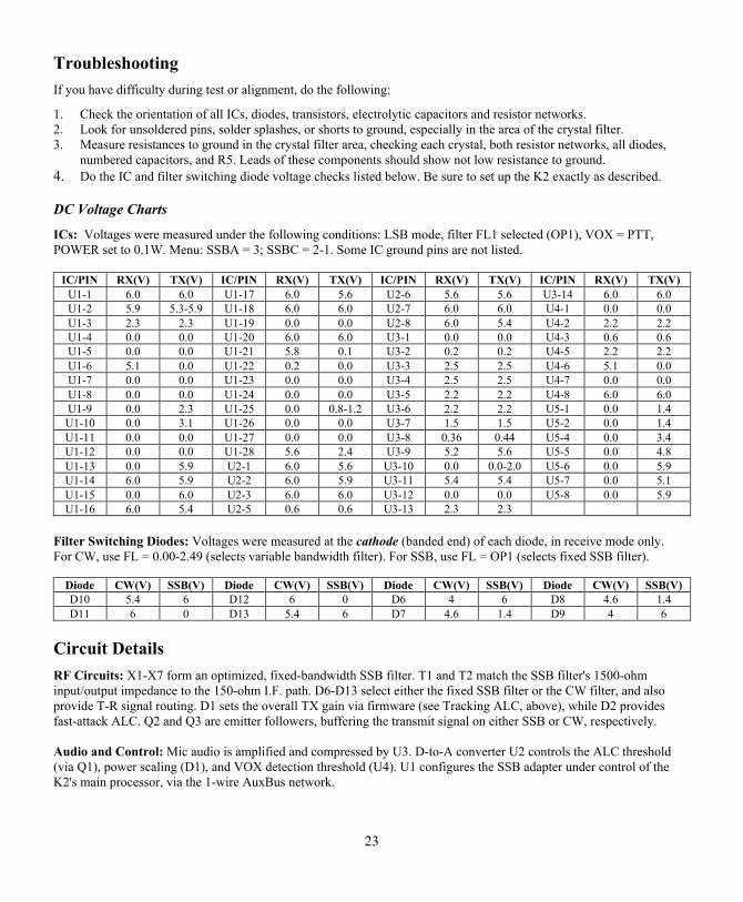
DC Voltage Charts
ICs: Voltages were measured under the following conditions: LSB mode, filter FL1 selected (OP1), VOX = PTT,POWER set to 0.1W. Menu: SSBA = 3; SSBC = 2-1. Some IC ground pins are not listed.
IC/PIN RX(V) TX(V) IC/PIN RX(V) TX(V) IC/PIN RX(V) TX(V) IC/PIN RX(V) TX(V)U1-1 6.0 6.0 U1-17 6.0 5.6 U2-6 5.6 5.6 U3-14 6.0 6.0U1-2 5.9 5.3-5.9 U1-18 6.0 6.0 U2-7 6.0 6.0 U4-1 0.0 0.0U1-3 2.3 2.3 U1-19 0.0 0.0 U2-8 6.0 5.4 U4-2 2.2 2.2U1-4 0.0 0.0 U1-20 6.0 6.0 U3-1 0.0 0.0 U4-3 0.6 0.6U1-5 0.0 0.0 U1-21 5.8 0.1 U3-2 0.2 0.2 U4-5 2.2 2.2U1-6 5.1 0.0 U1-22 0.2 0.0 U3-3 2.5 2.5 U4-6 5.1 0.0U1-7 0.0 0.0 U1-23 0.0 0.0 U3-4 2.5 2.5 U4-7 0.0 0.0U1-8 0.0 0.0 U1-24 0.0 0.0 U3-5 2.2 2.2 U4-8 6.0 6.0U1-9 0.0 2.3 U1-25 0.0 0.8-1.2 U3-6 2.2 2.2 U5-1 0.0 1.4U1-10 0.0 3.1 U1-26 0.0 0.0 U3-7 1.5 1.5 U5-2 0.0 1.4U1-11 0.0 0.0 U1-27 0.0 0.0 U3-8 0.36 0.44 U5-4 0.0 3.4U1-12 0.0 0.0 U1-28 5.6 2.4 U3-9 5.2 5.6 U5-5 0.0 4.8U1-13 0.0 5.9 U2-1 6.0 5.6 U3-10 0.0 0.0-2.0 U5-6 0.0 5.9U1-14 6.0 5.9 U2-2 6.0 5.9 U3-11 5.4 5.4 U5-7 0.0 5.1U1-15 0.0 6.0 U2-3 6.0 6.0 U3-12 0.0 0.0 U5-8 0.0 5.9U1-16 6.0 5.4 U2-5 0.6 0.6 U3-13 2.3 2.3
Filter Switching Diodes: Voltages were measured at the cathode (banded end) of each diode, in receive mode only.For CW, use FL = 0.00-2.49 (selects variable bandwidth filter). For SSB, use FL = OP1 (selects fixed SSB filter).
Diode CW(V) SSB(V) Diode CW(V) SSB(V) Diode CW(V) SSB(V) Diode CW(V) SSB(V)D10 5.4 6 D12 6 0 D6 4 6 D8 4.6 1.4D11 6 0 D13 5.4 6 D7 4.6 1.4 D9 4 6
Circuit Details
RF Circuits: X1-X7 form an optimized, fixed-bandwidth SSB filter. T1 and T2 match the SSB filter's 1500-ohminput/output impedance to the 150-ohm I.F. path. D6-D13 select either the fixed SSB filter or the CW filter, and alsoprovide T-R signal routing. D1 sets the overall TX gain via firmware (see Tracking ALC, above), while D2 providesfast-attack ALC. Q2 and Q3 are emitter followers, buffering the transmit signal on either SSB or CW, respectively.
Audio and Control: Mic audio is amplified and compressed by U3. D-to-A converter U2 controls the ALC threshold(via Q1), power scaling (D1), and VOX detection threshold (U4). U1 configures the SSB adapter under control of theK2's main processor, via the 1-wire AuxBus network.

24