knee rehabilitation monitor
TRANSCRIPT

1
Knee Rehabilitation Monitor
Design Review
Project #11:
Mark Hernandez
Nicholas Pesce
Gurmehar Lugani
Samik Mody (MBA)
TA: Cara Yang
ECE 445, Senior Design, Spring 2015

2
Table of Contents
1. Introduction ......................................................................................... 4
1.1 Statement of Purpose ..............................................................................................................4
1.2 Objectives ...............................................................................................................................4
1.2.1 Goals and Benefits ......................................................................................................4
1.2.1 Functions and Features ...............................................................................................4
2. Design .................................................................................................... 5
2.1 Block Diagrams ......................................................................................................................5
2.1.1 System Level Diagram ................................................................................................5
2.1.2 Software Diagrams......................................................................................................6
2.1.2.1 Device initialization and calibration ............................................................6
2.1.2.2 Everyday Mode ............................................................................................6
2.1.2.3 Inactivity Mode ............................................................................................7
2.1.2.3 Exercise Mode .............................................................................................8
2.1.2.3.1 Heel Slides ....................................................................................8
2.1.2.3.2 Straight Leg Raises .......................................................................9
2.2 Block Descriptions ...............................................................................................................10
2.2.1 Control Unit ..............................................................................................................10
2.2.2 Sensors ......................................................................................................................10
2.2.3 Power Source ............................................................................................................11
2.2.4 Feedback ...................................................................................................................11
3. Schematics .......................................................................................... 13
3.1 Microcontroller .....................................................................................................................13
3.2 Flex Sensor ...........................................................................................................................14
3.3 Accelerometer ......................................................................................................................16
3.4 Gyroscope .............................................................................................................................18
3.5 EMG .....................................................................................................................................20
3.6 Vibration Motors ..................................................................................................................24
3.7 Battery Management System ...............................................................................................26

3
4. Calculations and Simulations ........................................................... 28
4.1 Flex Sensor ...........................................................................................................................28
4.2 EMG .....................................................................................................................................30
5. Requirements and Verification ........................................................ 35
5.1 Control Unit ..........................................................................................................................35
5.2 Sensors .................................................................................................................................37
5.3 Feedback ...............................................................................................................................41
5.4 Power Source ........................................................................................................................42
6. Tolerance Analysis ............................................................................ 44
7. Cost and Schedule ............................................................................. 46
7.1 Cost Analysis ........................................................................................................................46
7.1.1 Labor .........................................................................................................................46
7.1.2 Parts...........................................................................................................................46
7.1.3 Grand Total ...............................................................................................................46
7.2 Weekly Schedule ..................................................................................................................47
8. Ethics and Safety ............................................................................... 48
8.1 IEEE Code of Ethics ............................................................................................................48
8.2 Safety ....................................................................................................................................48
9. References .......................................................................................... 49
Appendix ................................................................................................ 50

4
1. Introduction
1.1 Statement of Purpose
There are currently 100,000 ACL reconstruction knee surgeries and over 700,000 total
knee replacement surgeries annually in the United States.[1] Postoperative and preoperative
physical therapy are some of the most vital factors in recovering from these types of surgeries.
However, patients are at risk of re-injuring themselves at home when they are not under a
physical therapist’s supervision. Misguided home activity can potentially prolong the
rehabilitation period and add to the patient’s medical costs. We plan to develop a wearable knee
sleeve equipped with sensors that will aid the rehabilitation process by providing immediate
feedback to the user and allowing the physical therapist to monitor a patient’s knee health at
home. The feedback will allow patients to know if their actions at home are safe or if they are
performing their exercises correctly. The sensor data will let the physical therapists know if the
patients are following their prescribed home workout routine.
Many individuals have expressed interest in our project because they, or someone close
to them, have struggled with knee rehabilitation in the past. We believe that our idea can greatly
benefit those who will deal with this problem in the future – empowering them to rehabilitate
safely and effectively.
1.2 Objectives
1.2.1 Goals & Benefits:
● Accelerate the rehabilitation process for patients after knee surgery.
● Allow physical therapists to monitor a patient’s home activity and to enhance
supervised treatment.
● Provide user the feedback and the confidence to carry out home exercises.
● Reduce the chances of further injury.
1.2.2 Functions & Features:
● A wearable sleeve embedded with sensors that acquire information about a user’s
knee movements
● Different modes for knee movement analysis and feedback (everyday mode,
exercise mode, inactivity mode)
● Vibrational and visual feedback to immediately alert the user if an exercise is
being done properly or if there is an unhealthy knee movement being sensed
● Data storage for the user and physical therapist to track home activity using
additional software
● Carefully selected sensor placement and adaptive thresholds to address the
variations in knee structure among patients
● Compact all-in-one design for unobtrusive placement on knee

5
2. Design
2.1 Block Diagrams
2.1.1 System Level Diagram
Figure 1: System Level diagram of the device
Figure 1 shows the high level overview of the device. The device has four major blocks:
Sensors, Control Unit, Power source and Feedback. The Sensors block include the following
modules: flex sensor for measuring joint angle, the accelerometer and gyroscope to measure the
orientation of the joint and jerk it experiences, the EMG to measure the activity of the muscle
being monitored, and the push button/joystick for receiving user feedback for the navigation
menu on the LCD. The Control unit block includes the following modules: Microcontroller that
controls the entire device, the Storage device that stores diagnostic data of joint that is being
monitored. The feedback unit consists of the LCD on which the navigation menu will be
displayed, and the vibration motor which will alert the user if using the joint in an injurious
manner. The Power Source block consists of a battery health monitor and gates for controlling
power to other blocks in the device.
6
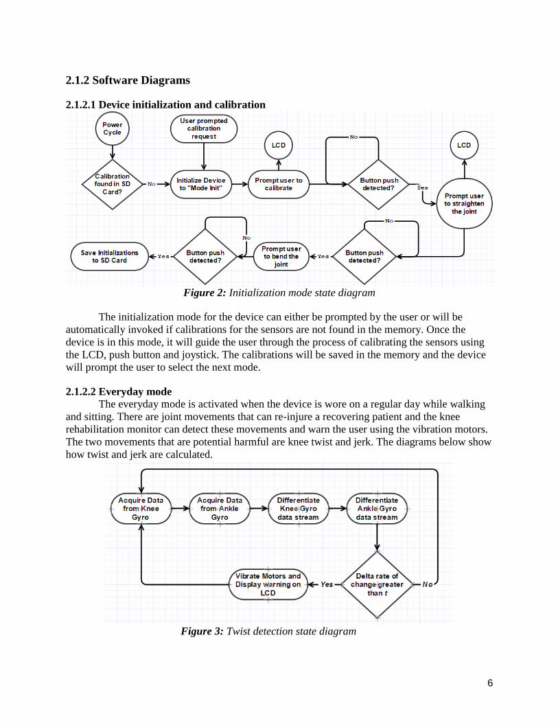
2.1.2 Software Diagrams
2.1.2.1 Device initialization and calibration
Figure 2: Initialization mode state diagram
The initialization mode for the device can either be prompted by the user or will be
automatically invoked if calibrations for the sensors are not found in the memory. Once the
device is in this mode, it will guide the user through the process of calibrating the sensors using
the LCD, push button and joystick. The calibrations will be saved in the memory and the device
will prompt the user to select the next mode.
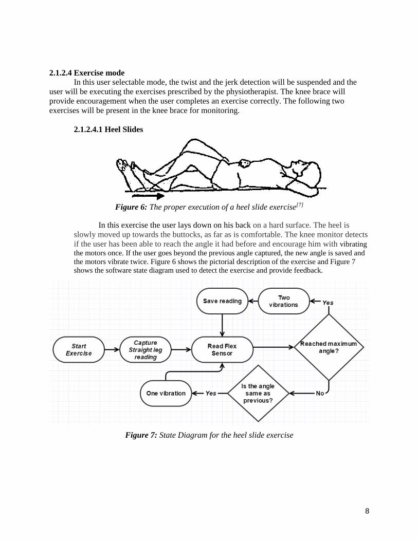
2.1.2.2 Everyday mode
The everyday mode is activated when the device is wore on a regular day while walking
and sitting. There are joint movements that can re-injure a recovering patient and the knee
rehabilitation monitor can detect these movements and warn the user using the vibration motors.
The two movements that are potential harmful are knee twist and jerk. The diagrams below show
how twist and jerk are calculated.
Figure 3: Twist detection state diagram

7
Figure 3 shows the state diagram from twist detection. The microcontroller detects the
twist of the knee by using a combination of gyroscopes on the knee and the ankle. If the change
in angle detected by the knee gyroscope with respect to the ankle gyroscope exceeds an
experimental threshold t, twist is detected and the user is warned by turning on the vibration
motors.
Figure 4: Jerk detection state diagram
Figure 4 shows the state diagram from jerk detection. The jerk is detected by the
accelerometer on the knee by measuring the derivative of acceleration on each of the axes. If the
derivative exceeds an experimental threshold t, jerk is detected and the user is warned by turning
on the vibration motors.
2.1.2.3 Inactivity Mode
This mode is responsible for detecting if the user has not moved the joint for a
programmable amount of time. Figure 5 shows the flex sensor reading is monitored and the user
is warned if the user has been in a position for prolonged period of time that can potentially harm
the joint.
Figure 5: Inactivity mode state diagram
8
2.1.2.4 Exercise mode
In this user selectable mode, the twist and the jerk detection will be suspended and the
user will be executing the exercises prescribed by the physiotherapist. The knee brace will
provide encouragement when the user completes an exercise correctly. The following two
exercises will be present in the knee brace for monitoring.
2.1.2.4.1 Heel Slides
Figure 6: The proper execution of a heel slide exercise[7]
In this exercise the user lays down on his back on a hard surface. The heel is
slowly moved up towards the buttocks, as far as is comfortable. The knee monitor detects
if the user has been able to reach the angle it had before and encourage him with vibrating
the motors once. If the user goes beyond the previous angle captured, the new angle is saved and
the motors vibrate twice. Figure 6 shows the pictorial description of the exercise and Figure 7
shows the software state diagram used to detect the exercise and provide feedback.
Figure 7: State Diagram for the heel slide exercise
9
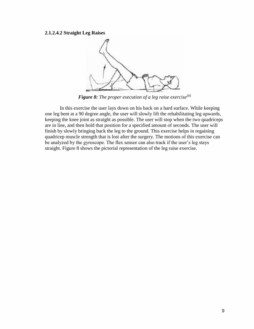
2.1.2.4.2 Straight Leg Raises
Figure 8: The proper execution of a leg raise exercise[8]
In this exercise the user lays down on his back on a hard surface. While keeping
one leg bent at a 90 degree angle, the user will slowly lift the rehabilitating leg upwards,
keeping the knee joint as straight as possible. The user will stop when the two quadriceps
are in line, and then hold that position for a specified amount of seconds. The user will
finish by slowly bringing back the leg to the ground. This exercise helps in regaining
quadricep muscle strength that is lost after the surgery. The motions of this exercise can
be analyzed by the gyroscope. The flex sensor can also track if the user’s leg stays
straight. Figure 8 shows the pictorial representation of the leg raise exercise.

10
2.2 Block Descriptions
2.2.2 Control Unit
The control unit is responsible for controlling all of the sensors, feedback devices, and
power source. It is also responsible for logging data from the sensors for post-processing and
analysis. battery maintenance purposes.
Microcontroller:
The microcontroller is responsible for controlling all the feedback devices in
the system as well as collecting and interpreting data from the sensors. It will also
control components of the power supply to manage the power consumption of the
device. It consists of the software that is capable of choosing modes of the device from
everyday mode, exercise mode or inactivity mode.
Data Storage:
The data storage will consist of a micro SD card with its associated circuitry to
interface it with the microcontroller via a serial communication. It is responsible for
saving data from the device for offline post processing.
2.2.2 Sensors
The sensor block contains devices that acquire real-time mechanical and physiological
information from the user’s knee. Additional circuitry for the sensors is implemented to allow
them to be interfaced with the microcontroller. Outputs from this block include critical sensory
data that describes the knee joint angle, knee motions, and quadricep muscle activity.
Flex Sensor:
The flex sensor is a thin strip, around 4.5 inches in length, that is used to monitor
the user’s knee joint angle. When the device is attached on the knee and bent, the flex
sensor circuitry will output unique output voltage which will describe the user’s range of
motion. Evaluation of the flex sensor data can help confirm that the user’s are reaching
their milestones in knee extension and knee flexion.
Accelerometer:
The accelerometer is a sensor positioned about 2 inches above the knee cap. It is
used to measure the acceleration that is being experienced by the leg along the x,y, and z
axes in space. The natural acceleration of gravity allows this sensor to give a
measurement of the leg’s orientation with respect to the ground. The accelerometer can
also give information about any abrupt changes in acceleration (jerk) that could be
dangerous for the user.
Gyroscope:
Two gyroscope sensors will be used in the design to measure the angular
acceleration of the upper and lower leg. One gyroscope is positioned about 2 inches
above the knee cap laying on the quadricep muscle. A second gyroscope chip is
positioned in the middle of the anterior side of the tibia (in front of the shin). The
combination of these sensors give information of unwanted lateral or medial movement

11
of the knee joint such as twisting. Additionally, the gyroscope data can characterize the
motions of repetitious leg workouts, especially the heel slides and leg raises mentioned in
section 2.1.2.4.
Electromyograph (EMG):
The EMG is a sensor that is used to detect the electrical muscle activity of the
quadricep. Three electrodes are used: one on the kneecap, one on the lower quadricep,
and one on the upper quadricep. A series of analog filters and bio-instrumentation
amplifiers will condition the EMG signal to only include quadricep muscle contractions.
Push Button and Joystick:
The push button and joystick directly interfaces with the LCD panel. This allows
the user to navigate a menu of device settings displayed on the LCD. The user can select
their preferred mode as well as calibrate baseline sensor measurements for exercise. 2.2.3 Power Source
The power source block provides power to all of the components in the system. A battery
is used as the main power source, while the battery management system (BMS) regulates the
power being distributed. An additional battery management feature allows the user to know
when the battery is running low.
9 Volt Battery:
The 9 volt battery serves as the main power source in the device. It will provide
the battery management circuitry with the raw power to be conditioned and allocated to
different blocks of the system.
Battery Management System (BMS):
The battery management system is responsible for distributing the power
throughout the system. Three voltage regulators in the BMS steps the battery voltage
down to coincide with the power supply requirements of the different devices in the
system. Input from the microcontroller can disable certain regulators when a certain
block is not needed. The BMS will also have a built-in feature that alerts the user when
the battery is about to die via LEDs.
2.2.4 Feedback
The feedback block consists of the devices that will alert the user with important
information regarding their knee health. Depending on the mode, the feedback systems activate
when the sensor data indicates unhealthy knee movements or correct knee movements for
exercises.
Vibration Motor:
Two vibration motors in the knee sleeve (one in the front of the leg, and one in the
back) provide haptic feedback to the user. In instances of unhealthy knee movements, the
vibration motors serve to immediately get the user’s attention. Additionally, the two
vibration motors will be activated at different times during exercise to provide the spatial
cues.

12
Liquid Crystal Display (LCD):
Once the vibration motors alerts the user initially, the LCD provides user with
more specific visual feedback. Messages are displayed on the LCD panel with the current
mode, suggestions, warnings, repetition counts, or positive feedback. It is also used to
debug the software during development of the prototype. The LCD interfaces with
microcontroller via 11 GPIOs. A Serial-in Parallel-out shift register would be used to
interface the LCD with microcontroller.

13
3. Schematics
3.1 Microcontroller
Figure 9: Microcontroller schematic without neighbouring components
Microcontroller Schematic Description
Inputs: Regulated 3.3VDC +/- 1% from Power Source
SPI bus input
Analog voltage from flex sensor
Analog voltage from EMG circuitry
Outputs: Digital levels 0 (0V +/- 1%) and 1 (Vcc +/- 1%) for chip selects, shift regs
SPI Bus data, and clock
Figure 9 depicts the microcontroller connections. It consists of a status LED
connected to Vcc which shows if the microcontroller is receiving power. C1 is
responsible for reducing noise in the input voltage and C2 allows the controller to save
critical data into flash before losing power.
14
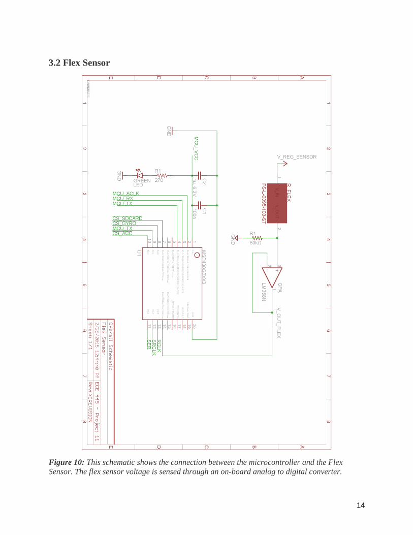
3.2 Flex Sensor
Figure 10: This schematic shows the connection between the microcontroller and the Flex
Sensor. The flex sensor voltage is sensed through an on-board analog to digital converter.

15
Flex Sensor Schematic Description
Inputs: Regulated 3.3 VDC +- 1% from Power Source
Outputs: Analog output voltage of the flex sensor circuit to Control Unit
The flex sensor acts as variable resistor which changes resistance when it is bent.
Higher angles of bending correspond to higher resistances. The circuit shown in Figure
10 allows an output voltage (related to the flex sensor resistance and bend angle) to be
interfaced with the microcontroller’s analog-to-digital converter. The flex sensor is
incorporated into a voltage divider circuit and put through an impedance buffer.
16
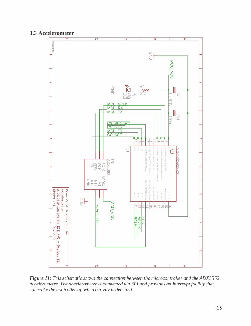
3.3 Accelerometer
Figure 11: This schematic shows the connection between the microcontroller and the ADXL362
accelerometer. The accelerometer is connected via SPI and provides an interrupt facility that
can wake the controller up when activity is detected.

17
Accelerometer Schematic Description
Inputs: Regulated 3.3 VDC +- 1% supply voltage from Power Source
SPI clock signal (SCLK) from Control Unit
SPI chip select bit (CS) from Control Unit
SPI master output, slave input signal (MOSI) from Control Unit
Outputs: SPI master input, slave output signal (MISO) to Control Unit
Interrupt signal (INT1) for activity detection to Control Unit
The digital 3-axis acceleration data from this sensor is interfaced with the
microcontroller’s SPI input pin for data analysis. Additionally, one of the interrupt bits
(INT1) is used to as a wake-up signal for the microcontroller. A built-in feature of the
accelerometer chip allows the activity detection; if leg movements are detected by the
accelerometer, the interrupt signal will take the microcontroller out of its low-power
mode, reactivating all of its normal functions and data storage.
18
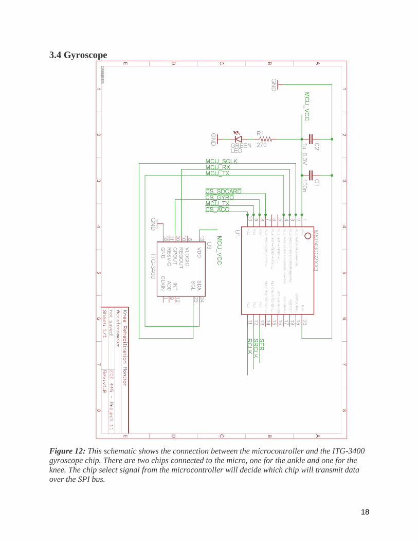
3.4 Gyroscope
Figure 12: This schematic shows the connection between the microcontroller and the ITG-3400
gyroscope chip. There are two chips connected to the micro, one for the ankle and one for the
knee. The chip select signal from the microcontroller will decide which chip will transmit data
over the SPI bus.

19
Gyroscope Schematic Description
Inputs: Regulated 3.3 VDC +- 1% supply voltage from Power Source
SPI clock signal (SCLK) from Control Unit
SPI chip select bit (nCS) from Control Unit
Outputs: SPI Serial Data Output (SDO) to Control Unit
The digital 3-axis angular acceleration data from this sensor is interfaced with the
microcontroller’s SPI input pin for data analysis. Two gyroscope chips are used on the
upper and lower leg in order to quantify unhealthy twisting motions. This is done by
evaluating the differences in angular acceleration between the two sensors.

20
3.5 EMG
Figure 13: The Bio-Instrumentation Amplifier internal circuitry model. All disconnected wires
are unused pins which are connected in the overall EMG circuit schematic but are left out here
for description purposes.
Input Voltage Drop across 2 Electrodes (V1-V2)
Output Vin*278 G = 278 V/V
The AD622 chip itself houses all of the circuitry seen in Figure 13 in a single IC. There
will be no physical diodes or resistors in this part of the circuit as these are included in the
AD622 package. It is important however to discuss the various components of this amplifier to
better understand its functionality. The diodes are all high power rating, pull down, laser cut
elements housed inside the AD622 chip to prevent voltage spikes from giving the user a shock.
This concept is more important during testing of this circuit element rather than in the
application of it due to the fact that the finished circuit will contain only DC power sources from
a low voltage battery minimizing the chance of a high voltage spike. The two resistors function
to limit the input current to be less than 60 mA which is the safe operating current of the AD622
package. Our design does not require monitoring of this input current as voltages originating at
the two input leads will be sufficiently small as to never exceed the required 60 mA. The
triangular box represents the pin-set of the AD622 chip and displays all 8 of the chip’s pins.

21
Figure 14: Band Pass Filter
Input Vout from AD622 with G = 278 V/V
Output Vout = Vin * 10 G = 10 V/V
As seen in Figure 14, the LM741 operational amplifier serves to both amplify and filter
the input voltage signal seen at R3. The output and input of this section of the schematic are left
unconnected due to the fact that this picture represents a modular component of a larger EMG
circuit element where input and output voltages are not determined. In this picture of the Band
Pass Filter circuit element, 4 external components are required and used along with the LM741
chip which houses only an operational amplifier. The capacitances and resistances must be
carefully chosen to open a frequency window of which all frequencies outside will be negated.
These values set not only the voltage gain for this circuit element but also the frequencies
attenuated.

22
Figure 15: High Pass Filter
Input Voltage from first LM741
Output Vout = Vin*10
Repeated in its use once more, the LM741 operational amplifier is used once again in a
high pass filter application to wipe DC components picked up from various levels of
amplification or processing. The bandpass filter does indeed account for DC value removal
through its lower end frequency cut-off of 20 Hz. However, some noise is still produced from
DC frequencies hovering below 4 Hz which are picked up from amplification. These values are
attenuated by this high pass filter. Not only does this filter remove the strong DC component
from the output signal, it also steps up the voltage again by -10 V/V. Because the output from
Figure 15 is amplified by -10 V/V, the gain from the second amplifier should be negative to
correct for positive voltage outputs. Stepping up the voltage by another 10 V/V finally places the
output reading in the range needed for subsequent labview filtering and testing; 0 to +2 volts.
23
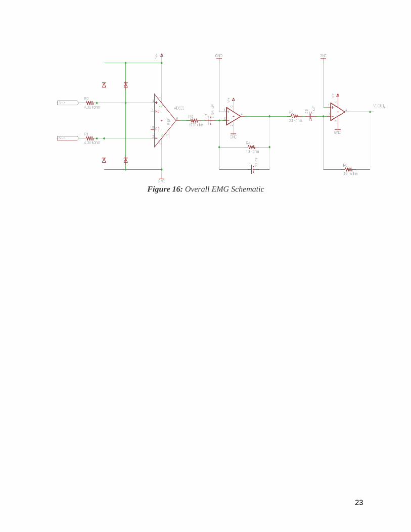
Figure 16: Overall EMG Schematic
24
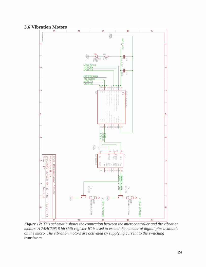
3.6 Vibration Motors
Figure 17: This schematic shows the connection between the microcontroller and the vibration
motors. A 74HC595 8 bit shift register IC is used to extend the number of digital pins available
on the micro. The vibration motors are activated by supplying current to the switching
transistors.

25
Vibration Motor Schematic Description
Inputs: Regulated 3.3 VDC +/- 1% supply voltage from Power Source
Enable bit to activate vibration from Control Unit
Outputs: None
When the enable signal from the microcontroller output is high, the transistor is
activated and current is allowed to flow from gate to drain. This will activate the
vibration motor which is being driven by the power supply.

26
3.7 Battery Management System
Battery Management System Schematic Description
Inputs: 9 volt battery voltage
Outputs: Regulated 3.3VDC +/- 1% voltage to Sensors
Regulated 3.3VDC +/- 1% voltage to Control Unit
Regulated 3.3VDC +/- 1% voltage to Feedback
Figure 18: The battery monitoring circuit
The circuit for the battery voltage monitoring is depicted in Figure 18. The Zener
diode is the most vital component in this circuit as it determines the cut-off voltage to
indicate that the battery is running low.[6] A Zener diode with a breakdown voltage of 6
VDC +/- 5% is used. When the battery voltage is above this breakdown voltage, the
Zener diode will conduct, activating the first transistor, and allowing the green LED to
light up. When the battery voltage falls below this breakdown voltage, the Zener diode
will not conduct, activating the second transistor, and allowing the red LED to light up.
27
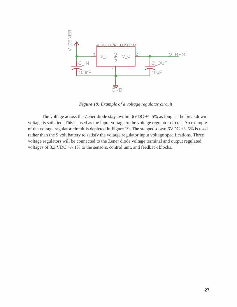
Figure 19: Example of a voltage regulator circuit
The voltage across the Zener diode stays within 6VDC +/- 5% as long as the breakdown
voltage is satisfied. This is used as the input voltage to the voltage regulator circuit. An example
of the voltage regulator circuit is depicted in Figure 19. The stepped-down 6VDC +/- 5% is used
rather than the 9 volt battery to satisfy the voltage regulator input voltage specifications. Three
voltage regulators will be connected to the Zener diode voltage terminal and output regulated
voltages of 3.3 VDC +/- 1% to the sensors, control unit, and feedback blocks.

28
4.1 Flex Sensor
Calculations for Flex Sensor Circuit:
Given the schematic for the flex sensor in Figure 10, the output voltage for the entire circuit is
essentially modeled as a voltage divider in Equation 1.
Eq. 1:
The resistance of the flex sensor (R_flex) varies depending on the angle in which it is
being bent. The datasheet for this device (FS-L-0095-103-ST) indicates that when the sensor is
completely flat, the resistance should measure 10k Ohms with a tolerance of +- 30%. When bent
180 degrees, the resistance should double to 20k Ohms +- 30%.
The output voltage of the flex sensor circuit is the parameter that is passed to the
microcontroller. In order to maximize the range of this output voltage parameter, a value for the
second resistor (R1) was chosen to be 14K ohms. This value was determined in Matlab, using a
maximum finding function given different R1 values ranging from 10K Ohms to 20k Ohms
shown in Equation 2.
Eq. 2:

29
Simulations for Flex Sensor Circuit:
Figure 20: Simulated flex sensor output voltage with different sensor resistances
The simulation in Figure 20 illustrates the voltage output response given an input voltage
of 3.3 VDC from the Power Source block, varying with different flex sensor resistances. Given
the 30% tolerance of the flex sensor resistance, the range in which we expect to see the output
voltage at angles 0-180 degrees is highlighted in green. The maximized voltage difference
between is calculated to be 0.5662 V when R2 = 14K ohms. Different knee joint angles will be
mapped to a unique output voltage threshold within this range to describe the user’s range of
motion.

30
4.2 EMG
Figure 21: High level block diagram describing components of the EMG detection circuitry
AD622 Texas Instruments Bio-Instrumentation Amplifier: The bio-instrumentation
amplifier is an AD622 Texas Instruments model. Gain is set through the use of an
external resistor across pins 1-8 seen in Figure 21 and discussed more in subsequent
calculation sections of this review.
LM741 Texas Instruments Operational Amplifier Band Pass Filter: The LM741 is
the operation amplifier chosen for this component of the physical EMG circuit design.
This amplifier is used as part of an active filtering element which removes frequencies
outside of a desired band. Features of the LM741 include output and input overload
protection as well as oscillation damping which reduces noise from amplification.
LM741 Texas Instruments Operational Amplifier High Pass Filter: The third block
in the high level logic block diagram describes the highpass filter needed for removal of
DC components. These DC values caused an unwanted offset in the output data which
was noisy. Specifically, the DC components removed were anything below 5 Hz.
Calculations regarding this block of the diagram will be discussed in the EMG
Calculations section of this review.
Calculations for Bio-Instrumentation Amplifier:
Eq. 3:
50.5
1GR k
G

31
Figure 22: Required Values of Gain Resistors
The chart in Figure 22 was taken from the datasheet for the AD622 Operational
Amplifier[12]. Gain is set by placing a resistance across pins 1-8 of the AD chip. The table
in Figure 22 displays different theoretical gain values as well as the actual values
empirically derived from setting a number of pre-determined resistances across pins 1-8.
For our application, a good starting gain is in the range of 200-500 volts. A gain greater
than these values will be amplified too much in subsequent steps of processing and will
result in output values greater than the desired 0 to +2V range. A good compromise is to
use a resistor with a value around 182 ohms in order to set the gain to be 278 V/V.
Calculations for Bandpass Filter:
Since frequencies outside of 20-300 Hz are undesired, the values of R1, R2, C1 and C2 were
specifically chosen. The gain needed to be 10 V/V in order to increase the order of magnitude of
the voltage gain from the AD622 amplifier by 1 order of 10. This conditions the voltage to be
stepped up one last time before being filtered with software. In the Figure 14, R1 corresponds to
R3, R2 corresponds to R4 and C1 and C2 correspond to C1 and C2 respectively.
Eq. 4:
2
1
RGain
R
Eq. 5:
1
1 1
1
2fc
R C
Eq. 6:
2
2 2
1
2fc
R C
R1 was chosen to be 1000 ohms
R2 was chosen to be 10 kohms

32
C1 was chosen to be approximately 7.95 uF
C2 was chosen to be approximately 53 nF
fc1 = 20.019 Hz
fc2 = 300.2923 Hz
Vout/Vin = -10 V/V
Calculations for High-Pass Filter:
Eq. 7:
2
1
RGain
R
Eq. 8: 1
2fc
RC
R corresponds to R5 = 33 kohm
R1 corresponds to R5 = 33 kohm
R2 corresponds to R6 = 330 kohm
C corresponds to C3 = 1 uF
fc = 4.822 Hz
The overall gain from this circuit is set in parts and works to increase the order of
magnitude of the signals received at the electrode leads. The gain from the bio-instrumentation
amplifier is about 200-500 V/V. The bandpass and highpass filters both have a gain of 10 V/V.
Thus in total, the signal is amplified by 20000 - 50000 V/V. This is ideal because the acquired
voltages are in micro or nanovolts.
10-9 * 20,000 = .0002 V
10-6 * 20,000 = .02 V
Simulation for EMG (Labview):
Figure 23: Labview Simulation Block Diagram for EMG
33
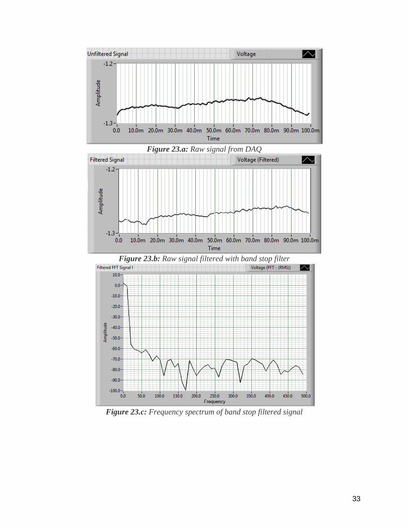
Figure 23.a: Raw signal from DAQ
Figure 23.b: Raw signal filtered with band stop filter
Figure 23.c: Frequency spectrum of band stop filtered signal
34
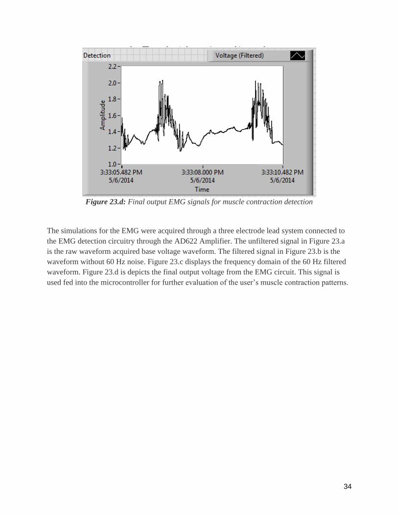
Figure 23.d: Final output EMG signals for muscle contraction detection
The simulations for the EMG were acquired through a three electrode lead system connected to
the EMG detection circuitry through the AD622 Amplifier. The unfiltered signal in Figure 23.a
is the raw waveform acquired base voltage waveform. The filtered signal in Figure 23.b is the
waveform without 60 Hz noise. Figure 23.c displays the frequency domain of the 60 Hz filtered
waveform. Figure 23.d is depicts the final output voltage from the EMG circuit. This signal is
used fed into the microcontroller for further evaluation of the user’s muscle contraction patterns.

35
5. Requirements and Verification
5.1 Control Unit
Requirements Verification Points
Microcontroller 20
a. The microcontroller is able to
program flash memory when
input voltage to the
microcontroller is 3.3V +- 5%
b. The microcontroller is able to
communicate over the Serial
Bus.
a.
● Attach the microcontroller input
supply to a power supply capable of
producing voltage of 3.3V.
● Attach the USB to the computer and
open Code Composer[10] software
provided by Texas Instruments
● Program the controller with the code
mentioned in Appendix C1
● Verify that the onboard LED toggles
every 1 sec.
b.
● Attach the microcontroller input
supply to a power supply capable of
producing voltage of 3.3V.
● Attach the USB to the computer and
open Code Composer[10] software
provided by Texas Instruments and
flash the controller with the code
provided in Appendix C2
● Open the Serial port emulation
software Tera Term[11]
● Send a string of at least 10 characters
using the Serial monitor in the
software and verify that the controller
is sending back the same string on the
serial monitor
● Repeat this test 10 times by sending
strings with different lengths and
characters. Verify the sent data is the
same as what is received from the
microcontroller

36
c. The microcontroller is able to
sense voltages via the analog
pins using the onboard ADC
within ranges of 0.0V - 3.3V
+/-5% with a precision of
3mV +/- 1%
d. Microcontroller can produce a
digital low of less than 0.7V
and a digital high of greater
than 1.3V
c.
● Attach the microcontroller input
supply to a power supply capable of
producing voltage of 3.3V.
● Attach a function generator to the pin
P1.1 on the microcontroller
● Attach the USB to the computer and
open Code Composer[10] software
provided by Texas Instruments and
flash the controller with the code
provided in Appendix C3
● Open the Serial port emulation
software Tera Term[11]
● Increase the voltage on the function
generator from 0.0V to 3.3V at
3.3mV increments
● Verify that the value broadcasted on
the serial monitor goes from 0 (for
0.0V) to 1023 (for 3.3V) linearly i.e.
for every 3.3mV increment, the value
on the serial monitor increases by 1.
d.
● Attach the microcontroller input
supply to a power supply capable of
producing voltage of 3.3V.
● Attach a multimeter to the pin P1.1 on
the microcontroller
● Attach the USB to the computer and
open Code Composer[10] software
provided by Texas Instruments and
flash the controller with the code
provided in Appendix C1
● Verify that the multimeter reads a low
voltage of less than 0.7V and a high
voltage of greater than 1.3V and the
low and the high is toggled every one
second. .
Data Storage 5
a. The data storage should be
able to Connect the Micro SD
to the SPI Bus. Use the
a. Remove the SD card from the device
and hook it up to a computer to check if
the file sizes are exactly what were

37
available SPI library to write a
file with size ranging from
1KiB to 1MiB with all zeros.
written and data was all zeros.
5.2 Sensors
Requirements Verification Points
Flex Sensor 10
a. The absolute maximum
ratings for the
microcontroller’s input pin
voltage is -0.3 VDC to Vcc +
0.3 VDC (Vcc = 3.3V +/-
1%). The flex sensor circuit
output must be:
-0.3V < vout,flex < 3.6 V
b. The microcontroller ADC
input resolution is
approximately 3 mV +/- 1%.
The flex sensor circuit output
voltage must change by a
minimum of 3 mV +/- 1%
when the angle of the flex
sensor is changed 10° in any
direction between 0° and 130°
|Δvout,flex| > 3 mV.
a.
● Assemble the complete flex sensor
circuit described in Figure 10 of
section 2.2.2 on a breadboard.
● Use multimeter to probe the voltage
between the output of the impedance
buffer (vout,flex) and ground.
● Bend the flex sensor from 0° to 180°
(pinch bend) and observe the output
voltage on the multimeter.
● Verify that the output voltage stays
within the maximum ratings of the
microcontroller.
b.
● Assemble the complete flex sensor
circuit described in Figure 10 of
section 2.2.2 on a breadboard.
● Use multimeter to probe the voltage
between the output of the impedance
buffer (vout,flex) and ground.
● Rest the flex sensor along the two
axes of a flat goniometer.
● Adjust the angle of the goniometer
and flex sensor by increments of 10°
● Record the observed voltage on the
multimeter, from 0° to 130°.
● Verify that the change in voltage |Δv|
exceeds 3 mV between every adjacent
datapoint.

38
Accelerometer 10
a. Supply voltage must be
between 1.8 VDC and 3.5
VDC.
b. The accelerometer must sense
an acceleration of 1g +/- 10%
on a single axis when
completely flat.
a.
● Attach the accelerometer input supply
to a DC power supply.
● Sweep the voltages from 1.0 VDC to
4.0 VDC
● Verify that the device is active within
the specified range.
b.
● Connect SPI output of the
accelerometer to microcontroller.
● Place sensor completely flat along
one axis.
● Verify that the microcontroller
indicates high values on one side (+1g
+/- 10% or 768 on the
microcontroller) and values close to
zero for the other sides (0g +/- 0.1g or
512 on the microcontroller).
● Rotate the sensor about a single axis.
● Verify that the values of one axis
increase and another axis decrease.
Gyroscope 10
a. Supply voltage must be
between 1.8 and 3.3VDC +/-
5%.
b. Gyroscope SPI output must
measure above 0g +/- 0.1g
when allowed to freefall.
a.
● Attach the gyroscope input supply to
a DC power supply.
● Sweep the voltages from 1.0VDC to
4.0VDC
● Verify that the device is active within
the specified range.
b.
● Connect SPI output of the gyroscope
to microcontroller.
● Attach gyroscope to a side of a
goniometer.
● Hold the goniometer at a 180° angle.
● Release the side with the sensor and
allow it to swing like a pendulum.
● Observe the sensor values through the
microcontroller and verify that the
angular acceleration of the

39
appropriate axis exceeds the given 0g
+/- 0.1g value during the initial free
fall.
EMG 15
a. Bio-instrumentation amplifier
must have an accurate gain
setting through a resistor
pinned between pins 1 and 8
of the AD622 Chip +/- 0.15%.
The AD622 is built to run on
6 mA of current at a
maximum over long
durations. Thus input voltages
must be limited to be less or
equal to a microvolt.
b. Bandpass filter gain must be
within 10V/V +/- 10%
c. Bandpass filter corner
frequencies of fc1 and fc2 must
be 20Hz +/- 10% and 300Hz
+/- 10% respectively
a.
● Place a resistor from the chart found
under section 2.2.6 and connect a
small test voltage (1 mV).
● Measure the output voltage of the
AD622 using a multimeter and record
the voltage.
● Calculate gain (Vout/Vin).
● Reference the chart found in Figure
22.
● Verify that the measured gain
matches theoretical values with a
tolerance of +/- 0.15 %. b. In order to verify that the bandpass filter
element is operating as intended, the
resistors and capacitors must be within a
tolerance of +/- 5% of the values listed
on the block diagram of this report. This
is to hold the gain at a constant and
predictable value.
● Hook up the circuit as described in
Block 2 and match resistor and
capacitor values.
● Measure the output voltage from the
bandpass filter circuit by supplying a
test voltage of 1 V.
● Measure Vout/Vin to calculate the
gain.
● The gain must be 10 V/V +/- 10% to
be predictable.
c. If the gain is within an acceptable range,
then the cutoff frequencies will be as
well.
● Calculate the cutoff frequencies using
the equations listed under the Block 2
Description section above
● Verify that the calculated high and
low cutoff frequencies are +/- 10 % of

40
d. High pass filter gain must be
within 10V/V +/- 10%
e. High pass filter cutoff
frequency fc = 4-5Hz
the desired 20-300 Hz band.
d. In order to verify that the high pass filter
element is operating as intended, the
resistors and capacitors must be within a
tolerance of +/- 5% of the values listed
on the block diagram of this report. This
is to hold the gain at a constant and
predictable value.
● Hook up the circuit as described in
Block 3 and match resistor and
capacitor values.
● Measure the output voltage by
supplying a test voltage of 1 V.
● Measure Vout/Vin to calculate the
gain.
● The gain must be 10 V/V +/- 10% to
be predictable.
e. If the gain is within an acceptable range,
then the cutoff frequencies will be as
well.
● Calculate the cutoff frequency using
the equations listed under the Block 3
Description section above
● Verify that the calculated frequency is
inside of the required 4-5 Hz range.
Joy Stick and Push Button 5
a. Connect the two
potentiometer in a voltage
divider circuit and sense the
drop across them.
b. Pull the microcontroller pin
where the push button is
connected to high. Connect
the other terminal of the push
button to ground with a 10k
ohm resistor in series.
a. Check if drop at full extension in both
negative and positive direction is 1.5V
+- 5% and at center position is 1.0V +-
5%
b. When the push button is pressed the
microcontroller should sense a drain to
ground on the pin the push button is
connected to. The pin should be pulled
to high again when the button is
depressed.

41
5.3 Feedback
Requirements Verification Points
Vibration Motors 5
a. Start voltage of 2.3 VDC, and
voltage range within 2.5 VDC
and 3.8 VDC.
a.
● Connect the vibration motor in series
to a DC power supply.
● Use multimeter to probe the voltage
across the vibration motor terminals.
● Sweep the voltages from 2.0 VDC to
4.5 VDC.
● Verify that the vibration motor
activates when the voltage exceeds
2.3 VDC +- 1%.
● Verify that the device is vibrating
within the appropriate voltage range
(2.5 - 3.8 VDC).
Liquid Crystal Display (LCD) 5
a. Connect the LCD data pins to
the microcontroller digital
pins. Run the software to
exercise each segment on the
LCD
a. Inspect visually if all segments light up
one by one.

42
5.4 Power Source
Requirements Verification Points
9 Volt Battery 5
a. The input to the battery health
monitoring circuit must be
above 6 VDC +/- 5%. The
battery must output a voltage
above this threshold.
a.
● Use multimeter to probe the voltage
across the positive and negative
terminals of the 9 volt battery.
● Verify that the measured voltage is
above the given threshold for the
battery health monitoring circuit.
Battery Management System 10
a. The voltage regulators have a
maximum input voltage rating
of 7 VDC. The voltage across
the 6V Zener diode must be
below 7 VDC.
vzener < 7 VDC
b. Vibration motor start voltage
is 2.3 VDC. The input voltage
range for the vibration motor
is 2.5VDC ~ 3.8VDC. The
voltage regulator output
voltage must be within these
constraints:
vout,reg > vstart = 2.3VDC
2.5 V < vout,reg < 3.8 V
a.
● Connect the negative terminal of the
diode to the V+ terminal of a DC
power supply.
● Connect the positive terminal of the
diode to the V- terminal of the DC
power supply.
● Use multimeter to probe the voltage
across the negative and positive
terminals of the Zener diode.
● Sweep the DC power supply voltage
from 6 VDC to 12 VDC.
● Verify that the voltage drop across the
Zener diode does not exceed 7 VDC
b.
● Connect voltage regulator input
voltage to V+ terminal of DC power
supply, and the GND pin to V-
terminal of DC power supply.
● Sweep DC power supply voltage
from 4 VDC to 7 VDC.
● Probe voltage regulator output with
multimeter.
● Verify that the output voltage is
greater than 2.3 VDC and within the
given input voltage range for the
vibration motors.

43
c. The microcontroller power
supply input pin operates at
voltage from 1.8 VDC to 3.5
VDC. The voltage regulator
must produce a voltage within
these constraints:
1.8 V < vout,reg < 3.5 V
d. The green LED must be on
and the red LED must be off
when the battery is above 6
VDC +/- 5%. The green LED
must be off and the red LED
must be on when the battery is
below 6 VDC +/- 5%.
c.
● Connect voltage regulator input
voltage to V+ terminal of DC power
supply, and the GND pin to V-
terminal of DC power supply.
● Sweep DC power supply voltage
from 4 VDC to 7 VDC.
● Probe voltage regulator output with
multimeter.
● Verify that the output voltage is
within the appropriate power supply
voltage range for the microcontroller.
d.
● Assemble the battery health
monitoring circuit described in Figure
18 on a breadboard, replacing the 9
Volt battery input with a DC power
supply input.
● Sweep the DC power supply voltage
from 4 VDC to 12 VDC.
● Verify that the LEDs are activated
and deactivated when the input
voltage transitions across the
threshold voltage.
44
6. Tolerance Analysis
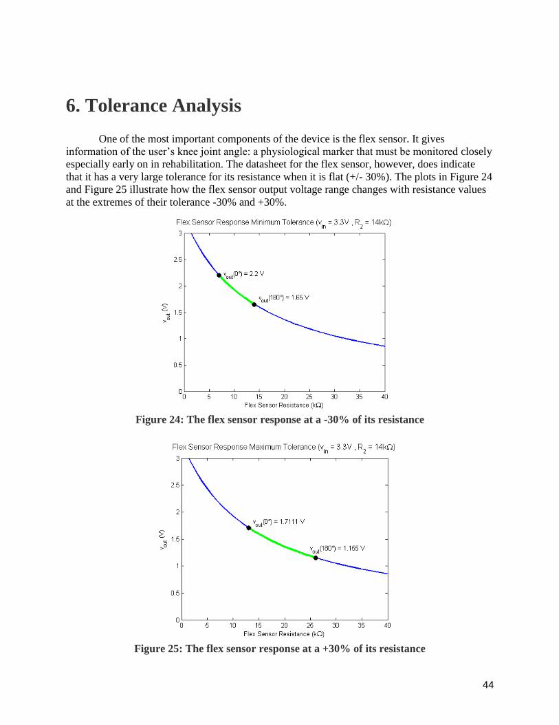
One of the most important components of the device is the flex sensor. It gives
information of the user’s knee joint angle: a physiological marker that must be monitored closely
especially early on in rehabilitation. The datasheet for the flex sensor, however, does indicate
that it has a very large tolerance for its resistance when it is flat (+/- 30%). The plots in Figure 24
and Figure 25 illustrate how the flex sensor output voltage range changes with resistance values
at the extremes of their tolerance -30% and +30%.
Figure 24: The flex sensor response at a -30% of its resistance
Figure 25: The flex sensor response at a +30% of its resistance

45
The output voltage range for the -30% and +30% tolerance came out to be 0.55 V and
0.56 V, respectively. The original simulation in Figure 20 with 0% tolerance measured an output
voltage range of 0.5662 V. Even despite this large tolerance range in the flex sensor resistance,
the important output voltage parameter does not change significantly. The output voltage range
for both extreme cases are still well within the resolution requirements of the microcontroller
ADC (3 mV). With this being said, the device does not require a flex sensor with a tighter
tolerance than +/- 30%.

46
7.0 Cost and Schedule
7.1 Cost analysis
7.1.1 Labor
Name Hourly
Rate
Total
Hours
Invested
Total = Hourly Rate
x 2.5 x Total Hours
Invested
Mark $30.00 225 $16,875
Nick $30.00 225 $16,875
Gurmehar $30.00 225 $16,875
Total 675 $50,525
7.1.2 Parts
Item Quantity Unit Cost Cost
Microcontroller MSP-EXP430G2 1 $13.74 $13.74
Flex Sensors SEN-10264 2 $12.95 $25.90
Gyroscope Accelerometer MPU 6500 1 $22.95 $22.95
Gyroscope ITG-3400 1 $19.99 $19.99
Electrodes 3 $1.95 $5.85
Vibrational Motors ROB-08449 2 $4.95 $9.90
Push Button & Joystick 1 $5.95 $5.95
LCD Panel: Basic 16x2 Character LCD -
Black on Green 3V 1 $13.95 $13.95
3.3 V Regulator LD1117V33 5 $0.99 $4.95
9 Volt Battery & Holder DUR-PC16049V 1 $2.95 $2.95
Shift Register IC Shift Register 8-Bit –
74HC595 4 $0.63 $2.52
Micro SD-Card 1 $20.00 $20.00
Additional Logic Circuitry 1 $5.00 $5.00
Flexible Knee Brace 1 $15.00 $15.00
Total $168.65
7.1.3 Grand Total
Section Total
Labor $50,525.00
Parts $168.65
Grand Total $50,693.65

47
7.2 Schedule
Week Task Responsibility
9-Feb
Finalize proposal Mark
Prepare mock design review Nick
Research and select microcontroller Gurmehar
16-Feb
Design review sign-up Mark
Finalize Mock Review Nick
Research and select sensors Gurmehar
23-Feb
Purchase sensors and run tests Mark
Purchase microcontroller and run tests Nick
Writing software for tests Gurmehar
2-March
Test power source and interface with sensors and feedback Mark
Discuss initial PCB design Nick
Program microcontroller with initial bring-up Gurmehar
9-March
Assemble the prototype circuit on a breadboard Mark
Finalize design for PCB Nick
Write state machines for different modes in the device Gurmehar
16-March
Test the prototype circuit on the breadboard Mark
Order PCB Nick
Verify and test state machines for different modes in the device Gurmehar
30-March
Finalize the initial progress report Mark
Prepare the mock demo Nick
Solder parts onto the final PCB Gurmehar
6-April
Run tests on output of microcontroller Mark
Finalize mock demonstration Nick
Embedded the device into a knee sleve Gurmehar
13-April
Ensure functionality and Demonstration sign-up Mark
Run tests on final project Nick
Finalize any software changes Gurmehar
20-April
Write a MATLAB script for post-processing Mark
Finalize demonstration Nick
Presentation sign-up Gurmehar
26-April
Finalize presentation Mark
Discuss initial draft of final paper Nick
Lab checkout Gurmehar
3-May
Field test the device Mark
Finalize final paper Nick
Future propositions for the device Gurmehar

48
8. Ethics and Safety
8.1 IEEE Code of Ethics
In order for our product to be professional, there are specific IEEE codes of Ethics that
we must consider:
1. to accept responsibility in making decisions consistent with the safety, health, and
welfare of the public, and to disclose promptly factors that might endanger the public or
the environment;
This point is particularly important to us because of the liability issues that come with a
health-related product. Since we are dealing with individuals who are already treating fragile
injuries, it is imperative that we thoroughly inform the users how to properly operate the device.
Improper use of the device due to poor documentation can increase the risk of the user’s further
injuring themselves.
3. to be honest and realistic in stating claims or estimates based on available data;
If we make false claims on what our product can evaluate (or how well they can evaluate)
a patient’s rehabilitation process, it could lead to improper medical treatment and incorrect
feedback. It is our responsibility to thoroughly test our product and ensure that claims are backed
up by definitive data.
7. to seek, accept, and offer honest criticism of technical work, to acknowledge and correct
errors, and to credit properly the contributions of others;
We have already started consulting with multiple physical therapists and businesspersons
to evaluate our design. Many changes were made to the initial proposal based on the feedback
from these individuals. We must honor their contributions of these collaborators, we will
acknowledge their efforts, either monetarily or in the final reports and documentation.
8.2 Safety
The ultimate goal of the knee rehabilitation monitor is to ensure the safety of patients as
they recover from knee surgeries. With that being said, we want to eliminate any additional
health hazards that the device may pose to the user. One obvious concern is the fact that the
system is in such close proximity to the patient’s skin. In order to avoid any possibilities of an
electrical shock, we plan to isolate the electrical components in insulated casings to ensure that
they are not directly in contact with the patient.
However, there is one component in our device that requires direct contact with the
patients skin: the electrodes. In this case, precautions will be taken while developing the EMG
circuitry. The protection circuit for the bio-instrumentation amp consists of diodes and capacitors
that give a safe path to ground if any spikes of voltage are introduced both the patient and the
circuit will be safe.

49
9. References
[1] Incidence of anterior cruciate ligament injury and other knee ligament injuries: A
national population-based study, Gianotti, Simon M. et al. Journal of Science and
Medicine in Sport , Volume 12 , Issue 6 , 622 - 627 February 25th 2015
[2] Datasheet for microcontroller: http://www.ti.com/lit/ds/symlink/msp430g2313.pdf
February 25th 2015
[3] Datasheet for flex sensor:
https://cdn.sparkfun.com/datasheets/Sensors/ForceFlex/FLEX%20SENSOR%20DATA%20S
HEET%202014.pdf February 25th 2015
[4] Datasheet for accelerometer: http://www.analog.com/media/en/technical-
documentation/data-sheets/ADXL362.pdf February 25th 2015
[5] Datasheet for gyroscope: http://www.invensense.com/mems/gyro/documents/PS-ITG-
3400A-00.pdf February 25th 2015
[6] Datasheet for vibration motor: https://www.sparkfun.com/datasheets/Robotics/310-
101_datasheet.pdf February 25th 2015
[7] Battery management circuit: http://www.electroschematics.com/6338/battery-level-
monitor/ February 25th 2015
[8] Heel slide workout: http://www.borgess.com/default.aspx?pId=2150 February 25th 2015
[9] Leg raise workout: http://cari-brokenknee.blogspot.com/2012/03/straight-leg-raise-
challenge.html February 25th 2015
[10] Code Composer Studio: http://www.ti.com/tool/ccstudio February 25th 2015
[11] Tera Term http://en.sourceforge.jp/projects/ttssh2/releases/ February 25th 2015
[12] Datasheet for EMG operational amplifiers: http://www.analog.com/media/en/technical-
documentation/data-sheets/AD622.pdf February 25th 2015

50
Appendix
#include <msp430g2553.h> // Initialize variables. This will keep count of how many cycles between LED toggles unsigned int i = 0; void main(void) { // Stop watchdog timer, // turns off the watchdog timer, which can reset the device after a // certain period of time. WDTCTL = WDTPW + WDTHOLD; // P1DIR configures the direction (DIR) of a port pin as an output or an input. P1DIR |= 0x01; // main loop for (;;) { // Toggle P1.0 using exclusive-OR operation (^=) P1OUT ^= 0x01; // Delay between LED toggles. for(i=0; i< 20000; i++); } }
Appendix C1: Code to toggle the on-baord LED of the micrcontroller
#include <msp430g2553.h> void main (void) { WDTCTL = WDTPW + WDTHOLD; // Stop watchdog timer CCTL0 = OUT; // TXD Idle as Mark TACTL = TASSEL_1 + MC_2; // ACLK, continuous mode P1SEL = TXD + RXD; P1DIR = TXD; // Mainloop for (;;) { RX_Ready(); // UART ready to RX one Byte _BIS_SR(LPM3_bits + GIE); // Enter LPM3 w/ interr until char RXed TX_Byte(); // TX Back RXed Byte Received } } // Function Transmits Character from RXTXData Buffer void TX_Byte (void) { BitCnt = 0xA; // Load Bit counter, 8data + ST/SP while (CCR0 != TAR) // Prevent async capture

51
CCR0 = TAR; // Current state of TA counter CCR0 += Bitime; // Some time till first bit RXTXData |= 0x100; // Add mark stop bit to RXTXData RXTXData = RXTXData << 1; // Add space start bit CCTL0 = CCIS0 + OUTMOD0 + CCIE; // TXD = mark = idle while ( CCTL0 & CCIE ); // Wait for TX completion } // Function Readies UART to Receive Character into RXTXData Buffer void RX_Ready (void) { BitCnt = 0x8; // Load Bit counter CCTL0 = SCS + OUTMOD0 + CM1 + CAP + CCIE; // Sync, Neg Edge, Cap } // Timer A0 interrupt service routine #pragma vector=TIMER0_A0_VECTOR __interrupt void Timer_A (void) { CCR0 += Bitime; // Add Offset to CCR0 // TX if (CCTL0 & CCIS0) // TX on CCI0B? { if ( BitCnt == 0) CCTL0 &= ~ CCIE; // All bits TXed, disable interrupt else { CCTL0 |= OUTMOD2; // TX Space if (RXTXData & 0x01) CCTL0 &= ~ OUTMOD2; // TX Mark RXTXData = RXTXData >> 1; BitCnt --; } } // RX else { if( CCTL0 & CAP ) // Capture mode = start bit edge { CCTL0 &= ~ CAP; // Switch from capture to compare mode CCR0 += Bitime_5; } else { RXTXData = RXTXData >> 1; if (CCTL0 & SCCI) // Get bit waiting in receive latch RXTXData |= 0x80; BitCnt --; // All bits RXed? if ( BitCnt == 0) { CCTL0 &= ~ CCIE; // All bits RXed, disable interrupt _BIC_SR_IRQ(LPM3_bits); // Clear LPM3 bits from 0(SR) } } } }
Appendix C2: Code to echo back the received Serial Data
52
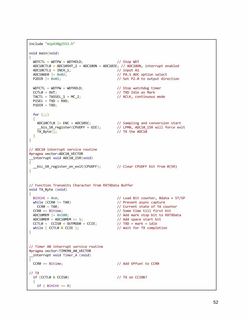
include "msp430g2553.h" void main(void) { WDTCTL = WDTPW + WDTHOLD; // Stop WDT ADC10CTL0 = ADC10SHT_2 + ADC10ON + ADC10IE; // ADC10ON, interrupt enabled ADC10CTL1 = INCH_1; // input A1 ADC10AE0 |= 0x02; // PA.1 ADC option select P2DIR |= 0x01; // Set P2.0 to output direction WDTCTL = WDTPW + WDTHOLD; // Stop watchdog timer CCTL0 = OUT; // TXD Idle as Mark TACTL = TASSEL_1 + MC_2; // ACLK, continuous mode P1SEL = TXD + RXD; P1DIR = TXD; for (;;) { ADC10CTL0 |= ENC + ADC10SC; // Sampling and conversion start __bis_SR_register(CPUOFF + GIE); // LPM0, ADC10_ISR will force exit TX_Byte(); // TX the ADC10 } } // ADC10 interrupt service routine #pragma vector=ADC10_VECTOR __interrupt void ADC10_ISR(void) { __bic_SR_register_on_exit(CPUOFF); // Clear CPUOFF bit from 0(SR) } // Function Transmits Character from RXTXData Buffer void TX_Byte (void) { BitCnt = 0xA; // Load Bit counter, 8data + ST/SP while (CCR0 != TAR) // Prevent async capture CCR0 = TAR; // Current state of TA counter CCR0 += Bitime; // Some time till first bit ADC10MEM |= 0x100; // Add mark stop bit to RXTXData ADC10MEM = ADC10MEM << 1; // Add space start bit CCTL0 = CCIS0 + OUTMOD0 + CCIE; // TXD = mark = idle while ( CCTL0 & CCIE ); // Wait for TX completion } // Timer A0 interrupt service routine #pragma vector=TIMER0_A0_VECTOR __interrupt void Timer_A (void) { CCR0 += Bitime; // Add Offset to CCR0 // TX if (CCTL0 & CCIS0) // TX on CCI0B? { if ( BitCnt == 0)

53
CCTL0 &= ~ CCIE; // All bits TXed, disable interrupt else { CCTL0 |= OUTMOD2; // TX Space if (ADC10MEM & 0x01) CCTL0 &= ~ OUTMOD2; // TX Mark ADC10MEM = ADC10MEM >> 1; BitCnt --; } } }
Appendix C3: Code to broadcast ADC reading onto the serial monitor