keysight technologies precise evaluation of input, output
TRANSCRIPT

Keysight TechnologiesPrecise Evaluation of Input, Output, and Reverse Transfer Capacitances of Power Devices
White Paper

The switching frequency in power conversion circuits is increasing. This is primarily to reduce the size of passive components such as smoothing capacitors and reactors. Accurate char-acterization of device parameters affecting switching performance become more important as higher switching frequencies increase power circuit switching losses. Let’s use the power MOSFET shown in Figure 1 as an example.
Gate resistance (Rg), input, output and reverse transfer capacitances (Ciss, Coss and Crss) are described in a device datasheet as typical parameters related to switching performance.
Rg and Crss dictate switching speed while Ciss determines driving condition. Power loss due to charging and discharging Coss is the primary component of switching loss in the case of a resonant converter. Crss and Coss have voltage dependency in the nano-farad range due to the power device’s depletion region modulating with applied varying operational voltages.
These capacitances are conventionally measured by LCR meter. However, the maximum volt-age of an integrated LCR voltage source is limited to around ±40 V. Therefore, most device data sheets do not include capacitance measurement data with more than ±40 V bias.
Circuit designers traditionally use curve fitting capacitance characteristics in their design work for voltages greater than 40 V. However, curve fitting is no longer viable due to complicated de-vice structures based upon trench or super junction structures. In addition, complicated manu-facturing processes induce additional variation in device performance. e.g. capacitance gap between high side FET and low side FET. Performance difference identification is key to device selection and failure analysis. Accordingly, for these reasons, device capacitance characteriza-tion from actual chip and module level measurements becomes essential.
Application notes provided by device manufacturers describe the power device capacitance measurement method. However, it is not a simple measurement. Many factors such as the determination of good peripheral circuit constants, measurement circuit compensation and appropriate measurement frequency have to be considered. This article discusses power device measurement methods and practical tips.
Hisao Kakitani and Ryo Takeda – Keysight Technologies International Japan G.K.
Increasing Importance of Capacitance Measurement
Figure 1. Three Capacitances of Power MOS FET
2 | Keysight | Precise Evaluation of Input, Output, and Reverse Transfer Capacitances of Power Devices - White Paper

Capacitance measurement on a three terminal device such as IGBT or MOSFET requires AC guarding plus peripheral circuits and an external bias source. Basic measurement set ups for a power MOSFET are discussed in this chapter.
Coss measurementFigure 2 shows the measurement circuit for output capacitance (Coss = Crss + Cds) of a MOSFET. High and low ports of the LCR meter are connected to the device after shorting the gate and the source terminals. The device impedance is calculated from applied voltage, Vm, and mea-sured current, Im. Coss voltage dependency, (+/-40 V) is measured by the integrated LCR meter voltage source.
Crss measurementFigure 3 shows the measurement circuit for reverse transfer capacitance (Crss) of a MOSFET. High and low ports of the LCR meter are connected to gate and drain terminals. The AC guard terminal of the LCR meter is connected to the source terminal. The AC guard directs current flow-ing through Cds directly to LCR meter circuit common without going through the current meter.
Basic Device Capacitance Measurement
Figure 2. Coss measurement by LCR meter
Figure 3. Crss measurement by LCR meter
3 | Keysight | Precise Evaluation of Input, Output, and Reverse Transfer Capacitances of Power Devices - White Paper

Ciss measurementFigure 4 shows the measurement circuit for input capacitance (Ciss) of a MOSFET. High and low ports of the LCR meter are connected to gate and source terminals. An external power supply is necessary to bias the drain terminal. A resistor or an inductor is necessary between the power supply and the drain in order to block the measurement AC signal flowing into the power supply. In addition, a large capacitor is necessary between drain and source terminals in order to short the AC measurement signal and to block the DC bias being applied to the drain terminal. The measure-ment signals flowing through Cgs and Crss are measured by the LCR current meter.
Rg measurementFigure 5 shows the measurement circuit for gate resistance (Rg) of a MOSFET. High and low ports of LCR meter are connected to gate and source terminals. Drain and source terminals can be shorted together. Occasionally, Rg is defined with the drain terminal open, as shown in Figure 5. The LCR meter is set to Rs-Cs mode and Rg is obtained from the measured input voltage (Vm) and output current (Im). The measurement frequency should be set to high in order to minimize the influence of Ciss. Gate voltage dependency of Ciss can be measured simultaneously with Rg by shorting drain and source terminals.
As discussed above the device connection and measurement circuitry wiring has to be changed for each different capacitance in three terminal device capacitance measurements.
Figure 4. Ciss measurement by LCR meter
Figure 5. Rg/Ciss measurement by LCR meter
4 | Keysight | Precise Evaluation of Input, Output, and Reverse Transfer Capacitances of Power Devices - White Paper

High voltage bias teeFor capacitance measurements on high voltage power devices an external high voltage DC source is necessary due to the inadequacy of the integrated +/-40 V LCR power supply.
A resistor or an inductor is necessary at the output of the external DC source to avoid leakage of the measurement AC signal. In addition, a blocking capacitor is mandatory to superimpose the measurement AC signal on the voltage bias source. A large capacitor is ideal to minimize mea-surement AC signal attenuation at the DUT terminal. However, too large a capacitor slows down measurement speed. Typically the appropriate blocking capacitor size is around ten times larger than the largest DUT capacitance. The capacitor type should be thin film as it has less voltage dependency. Figures 6, 7 and 8 are capacitance measurement circuits for high voltage devices and correspond to Figures 2, 3 and 4, respectively. A significant issue to consider is the risk of destroying measurement equipment due to the sudden inrush of voltage or current from the blocking capacitor when the DUT catastrophically fails. A protection circuit should be configured using a voltage clamp diode, a surge absorber and a resistor, (not shown in any of the figures). It is recommended that the breakdown voltage of the DUT is measured in advance of capacitance measurements and that capacitance bias voltage be well below the device breakdown voltage. Additionally, the measurement circuit has to be fully enclosed for safety reasons as the stored energy in the blocking capacitor is potentially fatal. Figure 9 shows hazardous energy range described in IEC60950-1 and IEC61010-1.
Challenges in High Voltage Device Capacitance Measurement
Figure 6. Coss measurement at High Voltage Bias
5 | Keysight | Precise Evaluation of Input, Output, and Reverse Transfer Capacitances of Power Devices - White Paper

Figure 7. Crss measurement at High Voltage Bias
Figure 8. Ciss measurement at High Voltage Bias
Figure 9. Capacitance Charge generally considered as safety
6 | Keysight | Precise Evaluation of Input, Output, and Reverse Transfer Capacitances of Power Devices - White Paper

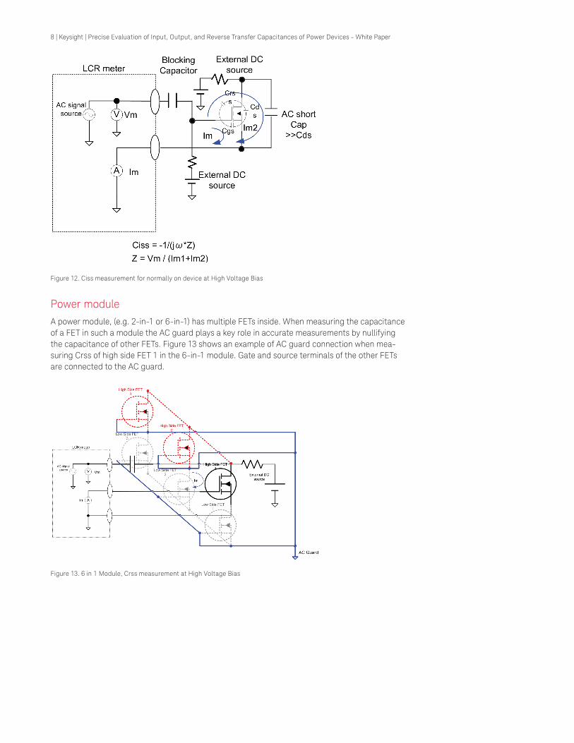
Normally on deviceFor depletion type devices, typically seen in GaN FET or SiC JFET, a negative voltage has to be applied to the gate terminal to turn off the device when making capacitance measurements. This measurement circuitry requires an additional blocking capacitor and an additional external DC source. Consequently it becomes complicated and troublesome to construct the test set up. Measurement circuitry examples are shown in Figures 10 and 11.
Figure 10. Coss measurement for normally on device at High Voltage Bias
Figure 11. Crss measurement for normally on device at High Voltage Bias
7 | Keysight | Precise Evaluation of Input, Output, and Reverse Transfer Capacitances of Power Devices - White Paper
Power moduleA power module, (e.g. 2-in-1 or 6-in-1) has multiple FETs inside. When measuring the capacitance of a FET in such a module the AC guard plays a key role in accurate measurements by nullifying the capacitance of other FETs. Figure 13 shows an example of AC guard connection when mea-suring Crss of high side FET 1 in the 6-in-1 module. Gate and source terminals of the other FETs are connected to the AC guard.
Figure 12. Ciss measurement for normally on device at High Voltage Bias
Figure 13. 6 in 1 Module, Crss measurement at High Voltage Bias
8 | Keysight | Precise Evaluation of Input, Output, and Reverse Transfer Capacitances of Power Devices - White Paper
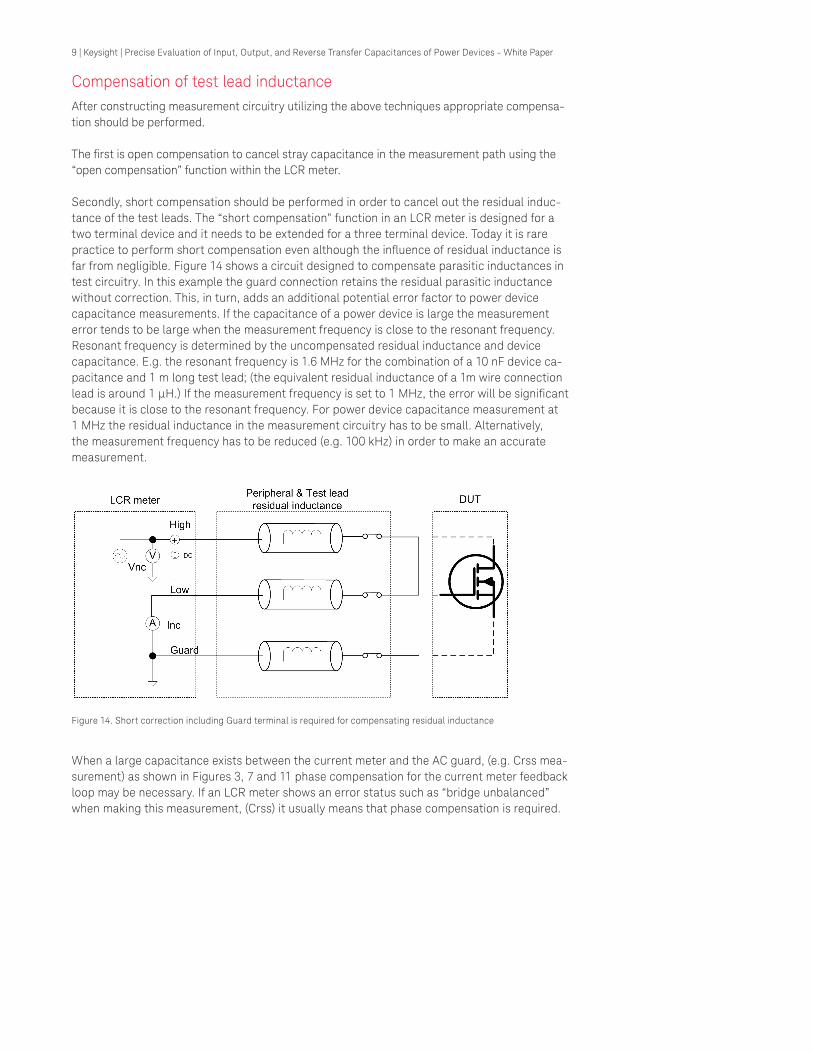
Compensation of test lead inductanceAfter constructing measurement circuitry utilizing the above techniques appropriate compensa-tion should be performed.
The first is open compensation to cancel stray capacitance in the measurement path using the “open compensation” function within the LCR meter.
Secondly, short compensation should be performed in order to cancel out the residual induc-tance of the test leads. The “short compensation” function in an LCR meter is designed for a two terminal device and it needs to be extended for a three terminal device. Today it is rare practice to perform short compensation even although the influence of residual inductance is far from negligible. Figure 14 shows a circuit designed to compensate parasitic inductances in test circuitry. In this example the guard connection retains the residual parasitic inductance without correction. This, in turn, adds an additional potential error factor to power device capacitance measurements. If the capacitance of a power device is large the measurement error tends to be large when the measurement frequency is close to the resonant frequency. Resonant frequency is determined by the uncompensated residual inductance and device capacitance. E.g. the resonant frequency is 1.6 MHz for the combination of a 10 nF device ca-pacitance and 1 m long test lead; (the equivalent residual inductance of a 1m wire connection lead is around 1 μH.) If the measurement frequency is set to 1 MHz, the error will be significant because it is close to the resonant frequency. For power device capacitance measurement at 1 MHz the residual inductance in the measurement circuitry has to be small. Alternatively, the measurement frequency has to be reduced (e.g. 100 kHz) in order to make an accurate measurement.
When a large capacitance exists between the current meter and the AC guard, (e.g. Crss mea-surement) as shown in Figures 3, 7 and 11 phase compensation for the current meter feedback loop may be necessary. If an LCR meter shows an error status such as “bridge unbalanced” when making this measurement, (Crss) it usually means that phase compensation is required.
Figure 14. Short correction including Guard terminal is required for compensating residual inductance
9 | Keysight | Precise Evaluation of Input, Output, and Reverse Transfer Capacitances of Power Devices - White Paper
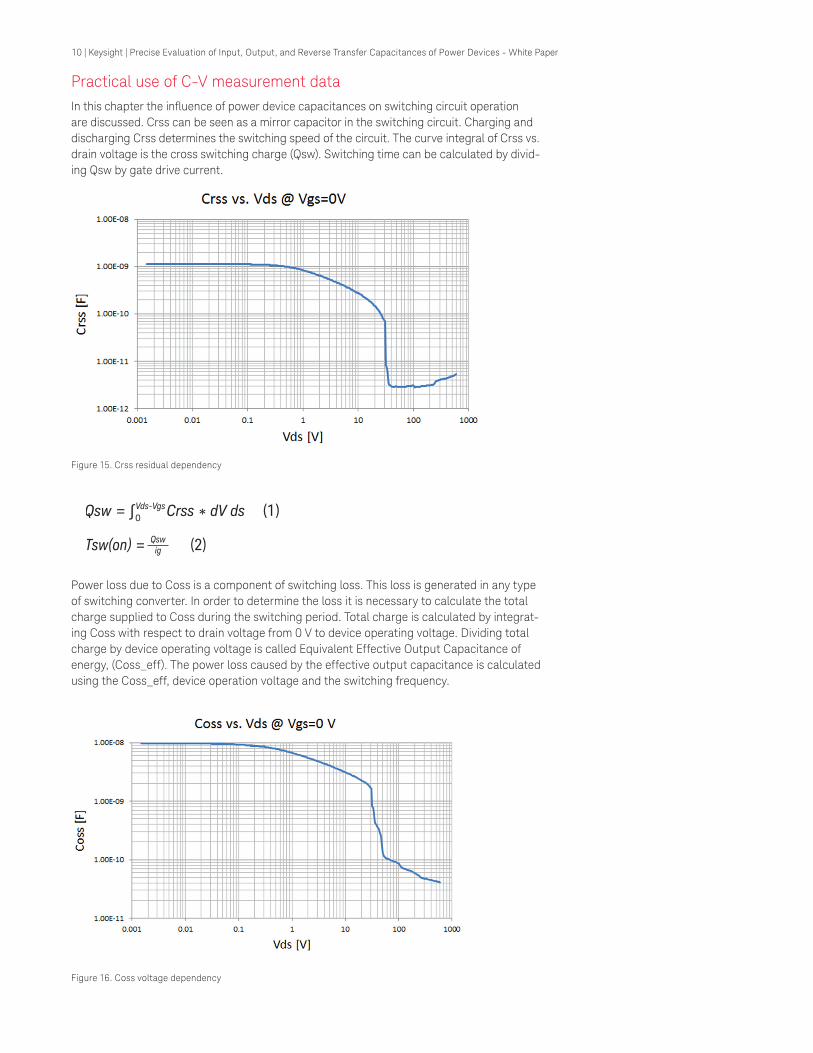
Practical use of C-V measurement dataIn this chapter the influence of power device capacitances on switching circuit operation are discussed. Crss can be seen as a mirror capacitor in the switching circuit. Charging and discharging Crss determines the switching speed of the circuit. The curve integral of Crss vs. drain voltage is the cross switching charge (Qsw). Switching time can be calculated by divid-ing Qsw by gate drive current.
Power loss due to Coss is a component of switching loss. This loss is generated in any type of switching converter. In order to determine the loss it is necessary to calculate the total charge supplied to Coss during the switching period. Total charge is calculated by integrat-ing Coss with respect to drain voltage from 0 V to device operating voltage. Dividing total charge by device operating voltage is called Equivalent Effective Output Capacitance of energy, (Coss_eff). The power loss caused by the effective output capacitance is calculated using the Coss_eff, device operation voltage and the switching frequency.
Figure 15. Crss residual dependency
Qsw = ;0 Crss * dV ds (1)Vds-Vgs
Tsw(on) = (2)Qsw
ig
Figure 16. Coss voltage dependency
10 | Keysight | Precise Evaluation of Input, Output, and Reverse Transfer Capacitances of Power Devices - White Paper

Ciss is a key parameter for gate drive circuit design. Drain voltage dependence on Ciss at Vgs = 0 V is initiated by its component Crss. Measurement of the gate drive charge when the device is off is straightforward. However, measuring drive capacitance when the device is on or when sweeping gate voltage from negative to positive in order to avoid unexpected turn on due to Vgs dependency on Ciss is essential. Both can be evaluated using the mea-surement set up shown in Figure 5.
Coss_eff = ;0 Coss * dV ds (3)1
VdsVds
Powerloss by Cosseff = * Cosseff * Vds2 * freq. (4)1
2
Figure 17. Ciss voltage dependency
11 | Keysight | Precise Evaluation of Input, Output, and Reverse Transfer Capacitances of Power Devices - White Paper
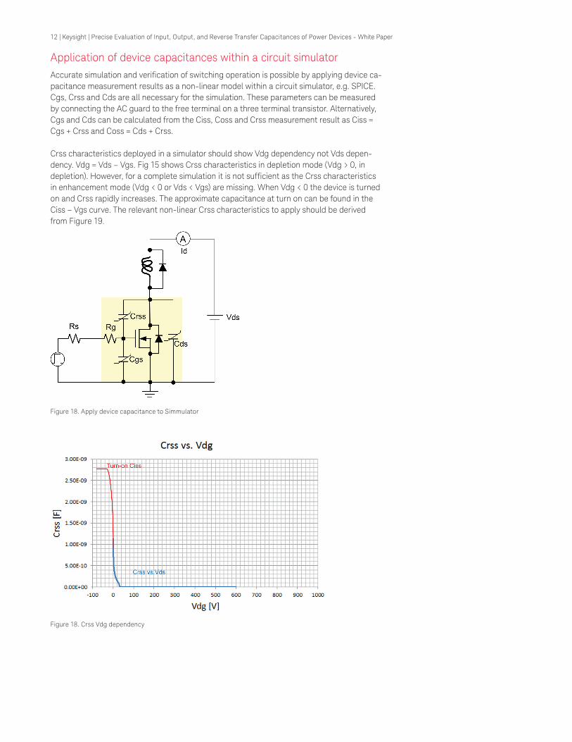
Application of device capacitances within a circuit simulatorAccurate simulation and verification of switching operation is possible by applying device ca-pacitance measurement results as a non-linear model within a circuit simulator, e.g. SPICE. Cgs, Crss and Cds are all necessary for the simulation. These parameters can be measured by connecting the AC guard to the free terminal on a three terminal transistor. Alternatively, Cgs and Cds can be calculated from the Ciss, Coss and Crss measurement result as Ciss = Cgs + Crss and Coss = Cds + Crss.
Crss characteristics deployed in a simulator should show Vdg dependency not Vds depen-dency. Vdg = Vds – Vgs. Fig 15 shows Crss characteristics in depletion mode (Vdg > 0, in depletion). However, for a complete simulation it is not sufficient as the Crss characteristics in enhancement mode (Vdg < 0 or Vds < Vgs) are missing. When Vdg < 0 the device is turned on and Crss rapidly increases. The approximate capacitance at turn on can be found in the Ciss – Vgs curve. The relevant non-linear Crss characteristics to apply should be derived from Figure 19.
Figure 18. Apply device capacitance to Simmulator
Figure 18. Crss Vdg dependency
12 | Keysight | Precise Evaluation of Input, Output, and Reverse Transfer Capacitances of Power Devices - White Paper
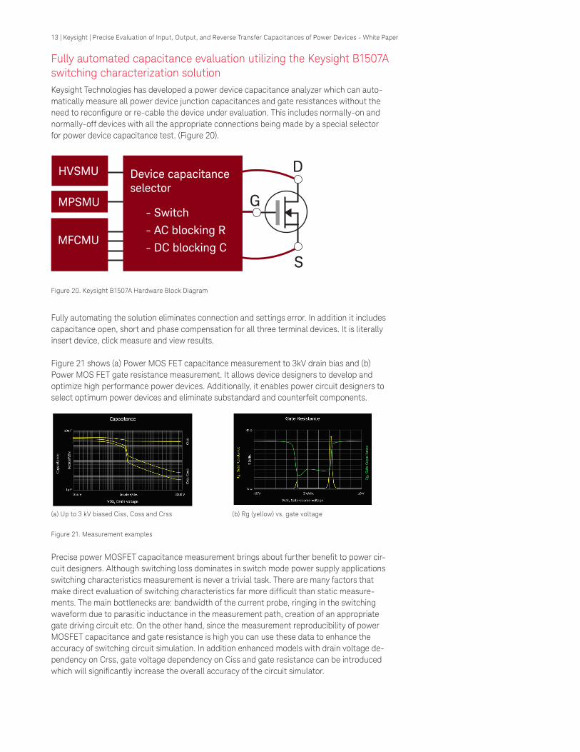
Keysight Technologies has developed a power device capacitance analyzer which can auto-matically measure all power device junction capacitances and gate resistances without the need to reconfigure or re-cable the device under evaluation. This includes normally-on and normally-off devices with all the appropriate connections being made by a special selector for power device capacitance test. (Figure 20).
Fully automating the solution eliminates connection and settings error. In addition it includes capacitance open, short and phase compensation for all three terminal devices. It is literally insert device, click measure and view results.
Figure 21 shows (a) Power MOS FET capacitance measurement to 3kV drain bias and (b) Power MOS FET gate resistance measurement. It allows device designers to develop and optimize high performance power devices. Additionally, it enables power circuit designers to select optimum power devices and eliminate substandard and counterfeit components.
Precise power MOSFET capacitance measurement brings about further benefit to power cir-cuit designers. Although switching loss dominates in switch mode power supply applications switching characteristics measurement is never a trivial task. There are many factors that make direct evaluation of switching characteristics far more difficult than static measure-ments. The main bottlenecks are: bandwidth of the current probe, ringing in the switching waveform due to parasitic inductance in the measurement path, creation of an appropriate gate driving circuit etc. On the other hand, since the measurement reproducibility of power MOSFET capacitance and gate resistance is high you can use these data to enhance the accuracy of switching circuit simulation. In addition enhanced models with drain voltage de-pendency on Crss, gate voltage dependency on Ciss and gate resistance can be introduced which will significantly increase the overall accuracy of the circuit simulator.
HVSMU
MFCMU
D
G
S
Device capacitance selector
- Switch
- AC blocking R
- DC blocking C
MPSMU
Figure 20. Keysight B1507A Hardware Block Diagram
Fully automated capacitance evaluation utilizing the Keysight B1507A switching characterization solution
Figure 21. Measurement examples
(a) Up to 3 kV biased Ciss, Coss and Crss (b) Rg (yellow) vs. gate voltage
13 | Keysight | Precise Evaluation of Input, Output, and Reverse Transfer Capacitances of Power Devices - White Paper
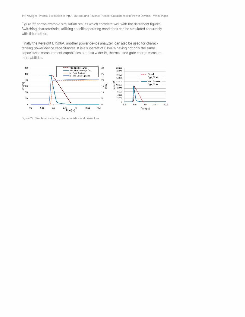
Figure 22 shows example simulation results which correlate well with the datasheet figures. Switching characteristics utilizing specific operating conditions can be simulated accurately with this method.
Finally the Keysight B1506A, another power device analyzer, can also be used for charac-terizing power device capacitances. It is a superset of B1507A having not only the same capacitance measurement capabilities but also wider IV, thermal, and gate charge measure-ment abilities.
Figure 22. Simulated switching characteristics and power loss
14 | Keysight | Precise Evaluation of Input, Output, and Reverse Transfer Capacitances of Power Devices - White Paper

For more information on Keysight Technologies’ products, applications or services, please contact your local Keysight office. The complete list is available at:www.keysight.com/find/contactus
Americas Canada (877) 894 4414Brazil 55 11 3351 7010Mexico 001 800 254 2440United States (800) 829 4444
Asia PacificAustralia 1 800 629 485China 800 810 0189Hong Kong 800 938 693India 1 800 112 929Japan 0120 (421) 345Korea 080 769 0800Malaysia 1 800 888 848Singapore 1 800 375 8100Taiwan 0800 047 866Other AP Countries (65) 6375 8100
Europe & Middle EastAustria 0800 001122Belgium 0800 58580Finland 0800 523252France 0805 980333Germany 0800 6270999Ireland 1800 832700Israel 1 809 343051Italy 800 599100Luxembourg +32 800 58580Netherlands 0800 0233200Russia 8800 5009286Spain 800 000154Sweden 0200 882255Switzerland 0800 805353
Opt. 1 (DE)Opt. 2 (FR)Opt. 3 (IT)
United Kingdom 0800 0260637
For other unlisted countries:www.keysight.com/find/contactus(BP-09-23-14)
15 | Keysight | Precise Evaluation of Input, Output, and Reverse Transfer Capacitances of Power Devices - White Paper
This information is subject to change without notice.© Keysight Technologies, 2014Published in USA, October 10, 20145992-0207ENwww.keysight.com
myKeysight
www.keysight.com/find/mykeysightA personalized view into the information most relevant to you.
www.axiestandard.orgAdvancedTCA® Extensions for Instrumentation and Test (AXIe) is an open standard that extends the AdvancedTCA for general purpose and semiconductor test. Keysight is a founding member of the AXIe consortium. ATCA®, AdvancedTCA®, and the ATCA logo are registered US trademarks of the PCI Industrial Computer Manufacturers Group.
www.lxistandard.org
LAN eXtensions for Instruments puts the power of Ethernet and the Web inside your test systems. Keysight is a founding member of the LXI consortium.
www.pxisa.org
PCI eXtensions for Instrumentation (PXI) modular instrumentation delivers a rugged, PC-based high-performance measurement and automation system.
Three-Year Warranty
www.keysight.com/find/ThreeYearWarrantyKeysight’s commitment to superior product quality and lower total cost of ownership. The only test and measurement company with three-year warranty standard on all instruments, worldwide.
Keysight Assurance Planswww.keysight.com/find/AssurancePlansUp to five years of protection and no budgetary surprises to ensure your instruments are operating to specification so you can rely on accurate measurements.
www.keysight.com/go/qualityKeysight Technologies, Inc.DEKRA Certified ISO 9001:2008 Quality Management System
Keysight Channel Partnerswww.keysight.com/find/channelpartnersGet the best of both worlds: Keysight’s measurement expertise and product breadth, combined with channel partner convenience.
www.keysight.com/find/b1507a