keysight 1gg7-4147 100 khz - 3 ghz broadband power …(for 60 seconds maximum) 300 °c esd1...
TRANSCRIPT
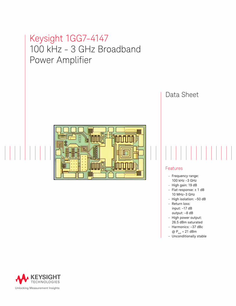
Keysight 1GG7-4147100 kHz - 3 GHz BroadbandPower Amplifier
Data Sheet
Features
– Frequency range: 100 kHz –3 GHz
– High gain: 19 dB – Flat response: ± 1 dB
10 MHz–3 GHz – High isolation: –50 dB – Return loss:
input: –17 dB output: –8 dB
– High power output: 26.5 dBm saturated
– Harmonics: –37 dBc @ Pout = 21 dBm
– Unconditionally stable

– Chip size: 1530 × 910 μm (60.2 × 35.8 mils)
– Chip size tolerance: ± 10 μm (± 0.4 mils)
– Chip thickness: 127 ± 15 μm (5.0 ± 0.6 mils)
– Pad dimensions: 75 × 75 μm (2.95 × 2.95 mils), or larger
Description
The 1GG7-4147 is a monolithic, wideband amplifier designed and fabricated using TSO’s DF7M GaAs MESFET process. It features low distortion and delivers (typically) 26.5 dBm saturated output power into 50Ω over at least a 100 kHz to 3.0 GHz frequency range. The 1GG7-4147 is fabricated using the Keysight Technologies, Inc. GaAs FET process.
Absolute maximum ratings1
Symbol Parameters/conditions Min Max Units
VD1 Stage 1 drain supply +8.5 Volts
VD2 Driver drain supply +5.1 Volts
VD3 Output drain supply +8.5 Volts
VSS Source supply –5.5 –3.5 Volts
Pin CW input power 23 dBm
Tcase Operating case temperature2 –55 90 °C
Tstg Storage temperature –65 165 °C
Tmax Maximum assembly temperature (for 60 seconds maximum)
300 °C
ESD1 Electrostatic discharge damage level (1.5 KW, 100 pF), Unbiased, applied to any IC bond pad
±400 Volts
ESD2 Electrostatic discharge damage level (1.5 KW, 100 pF), biased, output pad thru DC blocking cap
±1000 Volts
1. Operation in excess of any one of these conditions may result in permanent damage to this device. Parameter specified at TA = 25 °C, except for Tcase, Tstg, and Tmax.
2. Max continuous operating temp to achieve 1 × 10⁶ MTTF, while operating with VD1 = VD3 +8 V, VD2 = +5, VSS = –5 V. Derate MTTF by a factor of 2 for every 8 °C above this temperature.
02 | Keysight | 1GG7-4147 100 kHz - 3 GHz Broadband Power Amplifier - Data Sheet

RF specifications1
(VD1 = VD3 = +8 V, VD2 = +4.7 V, VSS = –5 V, Zin = Zo = 50Ω)
Symbol Parameters/conditions Min Typ Max Units
BW Guaranteed operating bandwidth2 .01 3 GHz
S21 Small signal gain 17 19 22 dB
ΔS21 Small signal gain flatness ±1 dB
RLin Input return loss –17 dB
RLout Output return loss –8 dB
S12 Reverse isolation –50 –50 dB
P1dB Output power at 1 db gain compression 25 dBm
Psat Saturated output power 25 26.5 dBm
H2,H3 Harmonics (Pout @ fundamental = 21 dBm) –35 –30 dBc
NF Noise figure (ƒ0 >100 MHz) 10 dB 10 dB
DC specifications/physical properties1
(Tchuck = 25 °C)2
Symbol Parameters/conditions Min Typ Max Units
ID1 First stage drain(VD1 = VD3 = +8 V, VD2 = +4.7 V, VSS = –5 V)
15 26 32 mA
ID2 Second stage drain current(VD1 = VD3 = +8 V, VD2 = +4.7 V, VSS = –5 V)
90 125 165 mA
ID3 Third stage drain current(VD1 = VD3 = +8 V, VD2 = +4.7 V, VSS = –5 V)
210 290 320 mA
ISS Source supply current(VD1 = VD3 = +8 V, VD2 = +4.7 V, VSS = –5 V)
45 71 95 mA
PDC DC power dissipation(VD1 = VD3 = +8 V, VD2 = +4.7 V, VSS = –5 V)
3.5 Watts
1. Data obtained from on–wafer measurements. All voltages specified at device pads.2. ID2 and ID3 values are temperature-sensitive parameters. Values measured in a packaged or heat-sunk condition will be up to 20 % lower than
measured on-wafer.
1. Data obtained from measurements on individual devices mounted in an Keysight 83040 series modular microcircuit package @ Tcase = 25 °C.2. Performance may be extended to lower frequencies through the use of off–chip circuitry. Upper corner frequency ≈ 4.3 GHz.
03 | Keysight | 1GG7-4147 100 kHz - 3 GHz Broadband Power Amplifier - Data Sheet

Applications
The 1GG7-4147 is designed for use as a broadband power amplifier in communication systems and microwave instrumentation. It is ideally suited for 100 kHz to 3 GHz applications where high output power, flat gain and low distortion are required.
Biasing
This device should be biased such that VSS = –5 V, VD1 = VD3 = +8 V, and VD2 = +4.7 V. This may be accomplished in several ways. Three separate supplies may be used to directly provide the required voltages. Alternatively, two supplies (–5, +8 V) may be used. In the latter case, the +4.7 V bias for VD2 may be derived from the +8 V supply with a variable resistor or regulator.
In addition to applying the proper voltages to the device, the off–chip impedances presented to VSS, VD2, and VD3 must be controlled. In particular, the VSS pad must be bypassed to provide an RF ground while VD2 and VD3 must be biased through a high impedance across the desired operating frequency range. This high impedance bias may be accomplished using chokes, active loads, or a combination of these components. VD1 bypassing is not critical.
To prevent damage to the device, the VSS supply should be turned on before the positive supplies during power up, and turned off after the positive supplies during power down. VSS must never be open circuited during operation.
The input and output of the 1GG7-4147 are DC coupled. The input pad will float at –5 V while the output pad is used to provide the VD3 bias and as a result will be at +8V. To prevent the disturbance of internal bias nodes, DC-blocking capacitors must be used on the input and output. The pads labelled VTH, M1, M2, and M3 are internal voltage monitor points and may be ignored.
Prolonged operation with maxi mum saturated output power into an open circuit should be avoided to prevent the possibility of long-term performance degration to the 1GG7-4147 device.
Assembly Techniques
Solder die attach using a AuSn solder preform is the recommended assembly method. Gold thermosonic wedge bonding with 0.7 mil wire is recommended for all bonds. Tool force should be 22 grams ±1 gram, stage temperature is 150 ± 2 °C, and ultrasonic power of 64 ± 1 dB and 76 ± 8 msec, respectively. The top and bottom metallization is gold.
GaAs MMICs are ESD sensitive. ESD preventive measures must be employed in all aspects of storage, handling, and assembly.
MMIC ESD precautions, handling considerations, die attach and bonding methods are criti- cal factors in successful GaAs MMIC performance and reliability.
The Keysight GaAs MMIC ESD, Die Attach and Bonding Guidelines - Application Note (5991-3484EN) provides basic information on these subjects.
04 | Keysight | 1GG7-4147 100 kHz - 3 GHz Broadband Power Amplifier - Data Sheet

VSS
VD1 M1 VD2
M2
M3RF
VD3
Input
RF Output
Notes— Chip top-side grounds and metalized chip
backside connected through conductive Vias
VSS Bypass
VTH
GND
Figure 1. 1GG7-4147 schematic
RoHS Compliance
This device is RoHS Compliant. This means the component meets the requirements of the European Parliament and the Council of the European Union Restriction of Hazard-ous Substances Directive 2011/65/EU, commonly known as RoHS. The six regulated substances are lead, mercury, cadmium, chromium VI (hexavalent), polybrominated biphenyls (PBB) and polybrominated biphenyl ethers (PBDE). RoHS compliance implies that any residual concentration of these substances is below the RoHS Directive’s maximum concentration values (MVC); being less than 1000 ppm by weight for all substances except for cadmium which is less than 100 ppm by weight.
05 | Keysight | 1GG7-4147 100 kHz - 3 GHz Broadband Power Amplifier - Data Sheet
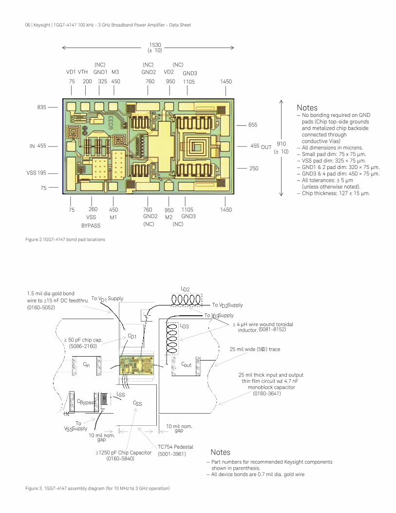
Notes— Part numbers for recommended Keysight components shown in parenthesis.— All device bonds are 0.7 mil dia. gold wire
To VD2 Supply
To VD3 Supply
To VD1 Supply
CD1
Cin Cout
CSSCBypass
LSS
25 mil thick input and output
≥ 50 pF chip cap.
10 mil nom.gap
25 mil wide (50 Ω ) trace
≥ 4 µH wire wound toroidal
10 mil nom.gap
inductor.
monoblock capacitor
≥1250 pF Chip Capacitor
R
VSS Supply
LD2
LD3
To
TC754 Pedestal(5001-3961)
thin film circuit w/≥ 4.7 nF
(0160-3641)
(5081-8152)
(0160-5840)
1.5 mil dia gold bondwire to ≥15 nF DC feedthru (0160-5052)
(5086-2160)
75 200 325 760 950
835
455
195
75
260 450 950760GND2
1105GND3
VD1 VTH(NC)
M3(NC) (NC)
VSS
M1 M2
655
455
250
1105450
VD2
OUTIN
VSS
BYPASS
75
1450
1450
910(± 10)
1530(± 10)
(NC) (NC)
GND2 GND1 GND3
Notes— No bonding required on GND
pads (Chip top-side grounds and metalized chip backside connected through conductive Vias)
— All dimensions in microns.— Small pad dim: 75 x 75 µm.— VSS pad dim: 325 × 75 μm.— GND1 & 2 pad dim: 320 × 75 μm.— GND3 & 4 pad dim: 450 × 75 μm.— All tolerances: ± 5 μm
(unless otherwise noted).— Chip thickness: 127 ± 15 μm.
Figure 2.1GG7-4147 bond pad locations
Figure 3. 1GG7-4147 assembly diagram (for 10 MHz to 3 GHz operation)
06 | Keysight | 1GG7-4147 100 kHz - 3 GHz Broadband Power Amplifier - Data Sheet
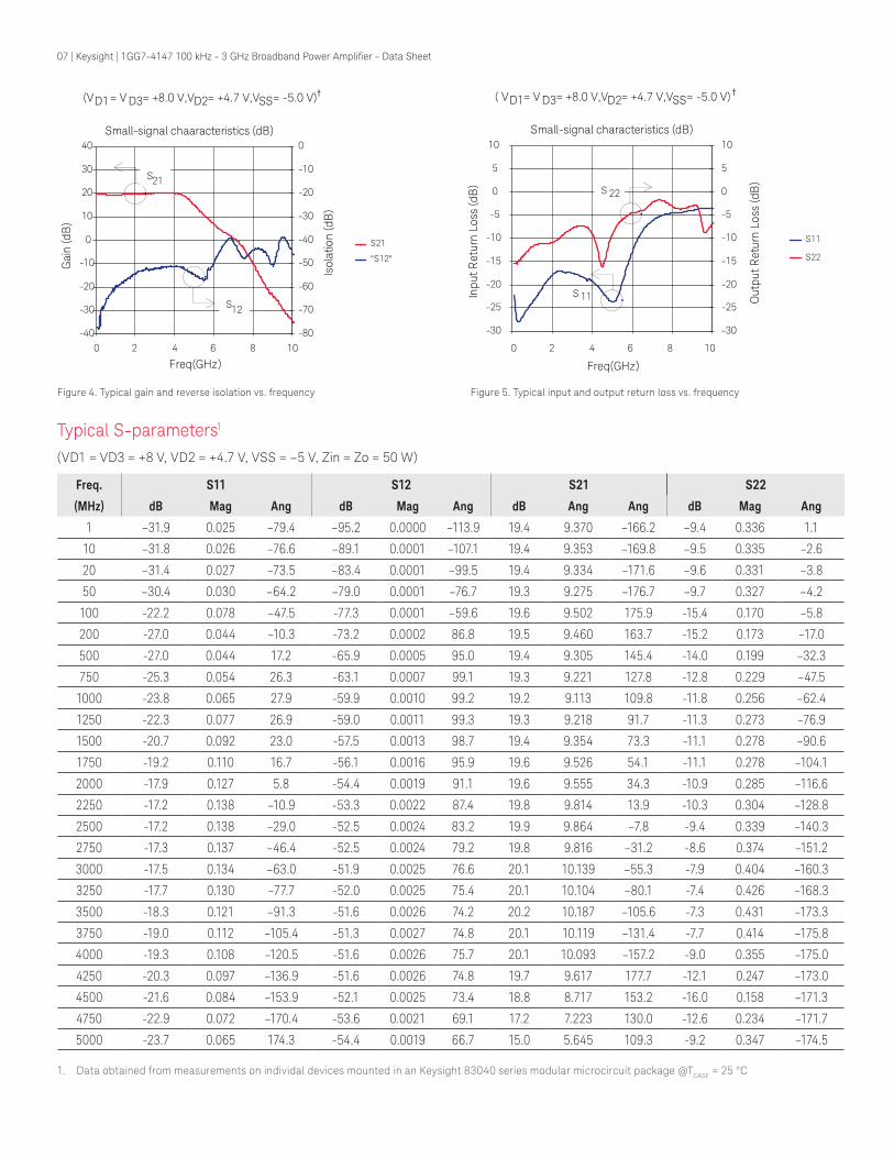
Small-signal characteristics (dB)
Freq(GHz)
Inpu
t Ret
urn
Loss
(dB
)
Out
put R
etur
n Lo
ss (d
B)
S11
S22
Small-signal chaaracteristics (dB)
Freq(GHz)
Gai
n (d
B)
Isol
atio
n (d
B)
S21
"S12"
(VD1 = V D3 = +8.0 V,VD2 = +4.7 V,VSS = -5.0 V)† ( VD1 = V D3 = +8.0 V,VD2 = +4.7 V,VSS = -5.0 V) †
-30
-25
-20
-15
-10
-5
0
5
10
-30
-25
-20
-15
-10
-5
0
5
10
0 2 4 6 8 10
S 11
S 22
-40
-30
-20
-10
0
10
20
30
40
0 2 4 6 8 10
-80
-70
-60
-50
-40
-30
-20
-10
0
S21
S12
Figure 4. Typical gain and reverse isolation vs. frequency Figure 5. Typical input and output return loss vs. frequency
Freq. S11 S12 S21 S22
(MHz) dB Mag Ang dB Mag Ang dB Ang Ang dB Mag Ang
1 –31.9 0.025 –79.4 –95.2 0.0000 –113.9 19.4 9.370 –166.2 –9.4 0.336 1.1
10 –31.8 0.026 –76.6 –89.1 0.0001 –107.1 19.4 9.353 –169.8 –9.5 0.335 –2.6
20 –31.4 0.027 –73.5 –83.4 0.0001 –99.5 19.4 9.334 –171.6 –9.6 0.331 –3.8
50 –30.4 0.030 –64.2 –79.0 0.0001 –76.7 19.3 9.275 –176.7 –9.7 0.327 –4.2
100 -22.2 0.078 –47.5 -77.3 0.0001 –59.6 19.6 9.502 175.9 -15.4 0.170 –5.8
200 -27.0 0.044 –10.3 -73.2 0.0002 86.8 19.5 9.460 163.7 -15.2 0.173 –17.0
500 -27.0 0.044 17.2 -65.9 0.0005 95.0 19.4 9.305 145.4 -14.0 0.199 –32.3
750 -25.3 0.054 26.3 -63.1 0.0007 99.1 19.3 9.221 127.8 -12.8 0.229 –47.5
1000 -23.8 0.065 27.9 -59.9 0.0010 99.2 19.2 9.113 109.8 -11.8 0.256 –62.4
1250 -22.3 0.077 26.9 -59.0 0.0011 99.3 19.3 9.218 91.7 -11.3 0.273 –76.9
1500 -20.7 0.092 23.0 -57.5 0.0013 98.7 19.4 9.354 73.3 -11.1 0.278 –90.6
1750 -19.2 0.110 16.7 -56.1 0.0016 95.9 19.6 9.526 54.1 -11.1 0.278 –104.1
2000 -17.9 0.127 5.8 -54.4 0.0019 91.1 19.6 9.555 34.3 -10.9 0.285 –116.6
2250 -17.2 0.138 –10.9 -53.3 0.0022 87.4 19.8 9.814 13.9 -10.3 0.304 –128.8
2500 -17.2 0.138 –29.0 -52.5 0.0024 83.2 19.9 9.864 –7.8 -9.4 0.339 –140.3
2750 -17.3 0.137 –46.4 -52.5 0.0024 79.2 19.8 9.816 –31.2 -8.6 0.374 –151.2
3000 -17.5 0.134 –63.0 -51.9 0.0025 76.6 20.1 10.139 –55.3 -7.9 0.404 –160.3
3250 -17.7 0.130 –77.7 -52.0 0.0025 75.4 20.1 10.104 –80.1 -7.4 0.426 –168.3
3500 -18.3 0.121 –91.3 -51.6 0.0026 74.2 20.2 10.187 –105.6 -7.3 0.431 –173.3
3750 -19.0 0.112 –105.4 -51.3 0.0027 74.8 20.1 10.119 –131.4 -7.7 0.414 –175.8
4000 -19.3 0.108 –120.5 -51.6 0.0026 75.7 20.1 10.093 –157.2 -9.0 0.355 –175.0
4250 -20.3 0.097 –136.9 -51.6 0.0026 74.8 19.7 9.617 177.7 -12.1 0.247 –173.0
4500 -21.6 0.084 –153.9 -52.1 0.0025 73.4 18.8 8.717 153.2 -16.0 0.158 –171.3
4750 -22.9 0.072 –170.4 -53.6 0.0021 69.1 17.2 7.223 130.0 -12.6 0.234 –171.7
5000 -23.7 0.065 174.3 -54.4 0.0019 66.7 15.0 5.645 109.3 -9.2 0.347 –174.5
Typical S-parameters1
(VD1 = VD3 = +8 V, VD2 = +4.7 V, VSS = –5 V, Zin = Zo = 50 W)
1. Data obtained from measurements on individal devices mounted in an Keysight 83040 series modular microcircuit package @TCASE = 25 °C
07 | Keysight | 1GG7-4147 100 kHz - 3 GHz Broadband Power Amplifier - Data Sheet

Additional 1GG7-4147 performance characteristics1
( VD1 = V D3 = +8 V, V D2 = +4.7 V,V SS = –5 V)
( VD1 = V D3 = +8 V, V D2 = +4.7 V,V SS = -5 V) ( VD1 = V D3 = +8 V, V D2 = +4.7 V,V SS = -5 V)
( VD1 = VD3 = +8 V, VD2 = +4.7 V,VSS = -5 V)
High-band noise figure performance
6.00
8.00
10.00
12.00
14.00
16.00
18.00
20.00
22.00
24.00
26.00
0.0100 0.1000 1.0000 10.0000Frequency (GHz)
Noi
se F
igur
e (d
B)
Output power vs. frequency
22
23
24
25
26
27
28
29
30
0 1 2 3 4 50 1 2 3 4 5
Freq (GHz)
Out
put
Pow
er (
dBm
)
Psat
P-1dB
Harmonic performance vs. frequency
20
30
40
50
60
70
80
90
100
Freq (GHz)
2nd,
3rd
Har
m (d
Bc)
2nd harmonics
3rd harmonics
Gain vs. temperature
25
26
27
28
29
30
31
32
0.15 0.5 1 2 3 4 4.5
Frequency (GHz)
Gai
n (d
B) -15 ˚C
0 ˚C45 ˚C70 ˚C
1. All data measured on individual devices mounted on a Keysight 83040 series modular microcircuit package @ TCASE = 25 °C, except where noted.
Figure 6. Typical small-signal gain vs. temperature
Figure 8. Typical 1 dB gain compression and saturated output power vs. frequency
Figure 7. Typical noise figure vs. frequency
Figure 9. Typical second and third harmonics vs. fundamental frequency at Pout = 21 dBm
08 | Keysight | 1GG7-4147 100 kHz - 3 GHz Broadband Power Amplifier - Data Sheet
This data sheet contains a variety of typical and guaranteed performance data. The information supplied should not be interpreted as a complete list of circuit specifications. Customers considering the use of this, or other Keysight Technologies GaAs ICs, for their design should obtain the current production specifications from Keysight. In this data sheet the term typical refers to the 50th percentile performance. For additional information contact Keysight at [email protected].
The product described in this data sheet is RoHS Compliant. See RoHS Compliance section for more details.
09 | Keysight | 1GG7-4147 100 kHz - 3 GHz Broadband Power Amplifier - Data Sheet
myKeysightwww.keysight.com/find/mykeysightA personalized view into the information most relevant to you.
Keysight Serviceswww.keysight.com/find/serviceKeysight Services can help from acquisition to renewal across your instrument’s lifecycle. Our comprehensive service offerings—one-stop calibration, repair, asset management, technology refresh, consulting, training and more—helps you improve product quality and lower costs.
Keysight Channel Partnerswww.keysight.com/find/channelpartnersGet the best of both worlds: Keysight’s measurement expertise and product breadth, combined with channel partner convenience.
For more information on Keysight Technologies’ products, applications or services, please contact your local Keysight office. The complete list is available at:www.keysight.com/find/contactus
Americas Canada (877) 894 4414Brazil 55 11 3351 7010Mexico 001 800 254 2440United States (800) 829 4444
Asia PacificAustralia 1 800 629 485China 800 810 0189Hong Kong 800 938 693India 1 800 11 2626Japan 0120 (421) 345Korea 080 769 0800Malaysia 1 800 888 848Singapore 1 800 375 8100Taiwan 0800 047 866Other AP Countries (65) 6375 8100
Europe & Middle EastAustria 0800 001122Belgium 0800 58580Finland 0800 523252France 0805 980333Germany 0800 6270999Ireland 1800 832700Israel 1 809 343051Italy 800 599100Luxembourg +32 800 58580Netherlands 0800 0233200Russia 8800 5009286Spain 800 000154Sweden 0200 882255Switzerland 0800 805353
Opt. 1 (DE)Opt. 2 (FR)Opt. 3 (IT)
United Kingdom 0800 0260637
For other unlisted countries:www.keysight.com/find/contactus(BP-06-08-16)
DEKRA CertifiedISO9001 Quality Management System
www.keysight.com/go/qualityKeysight Technologies, Inc.DEKRA Certified ISO 9001:2015Quality Management System
This information is subject to change without notice.© Keysight Technologies, 2016Published in USA, October 3, 20165992-1855ENwww.keysight.com
www.keysight.com/find/mmic
Evolving Our unique combination of hardware, software, support, and people can help you reach your next breakthrough. We are unlocking the future of technology.
From Hewlett-Packard to Agilent to Keysight