kathy palumbo, ceo and founder - dave kendrick, pcb ...pcbwizards.com/sddc/ipcdcmtgaug_oc.pdf ·...
TRANSCRIPT

David Hoover, Field Application Eng -
Orange County Chapter of the IPC Designers Council, Inc.presents: Cause and Effect – How little design issues can cause big headaches
to assemblers and fabricators.
Kathy Palumbo, CEO and Founder -
Dave Kendrick, PCB Designer -

Key Issues for Discussion(from a fabrication perspective)
� Bow and Twist •Unbalanced Stackups – What are the Causes?
–Odd Number of Layers–Nonsymmetrical Dielectrics or Material Types
Example:
� 5 Layers
� Imbalanced Dielectrics
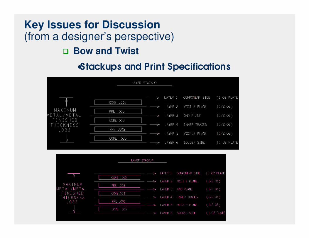
Key Issues for Discussion(from a designer’s perspective)
� Bow and Twist
•Stackups and Print Specifications

Key Issues for Discussion -(from a fabrication perspective)
� Bow and Twist
•Unbalanced Stackups – What are the Causes?–Unbalanced Copper Foil Weights
–Unbalanced Copper Distribution on the Layers (circuitry)
� Copper Foil Weights
� Unbalanced Circuitry
(e.g., RF and digital designs that have large open laminate areas or large metal shield/planes areas)
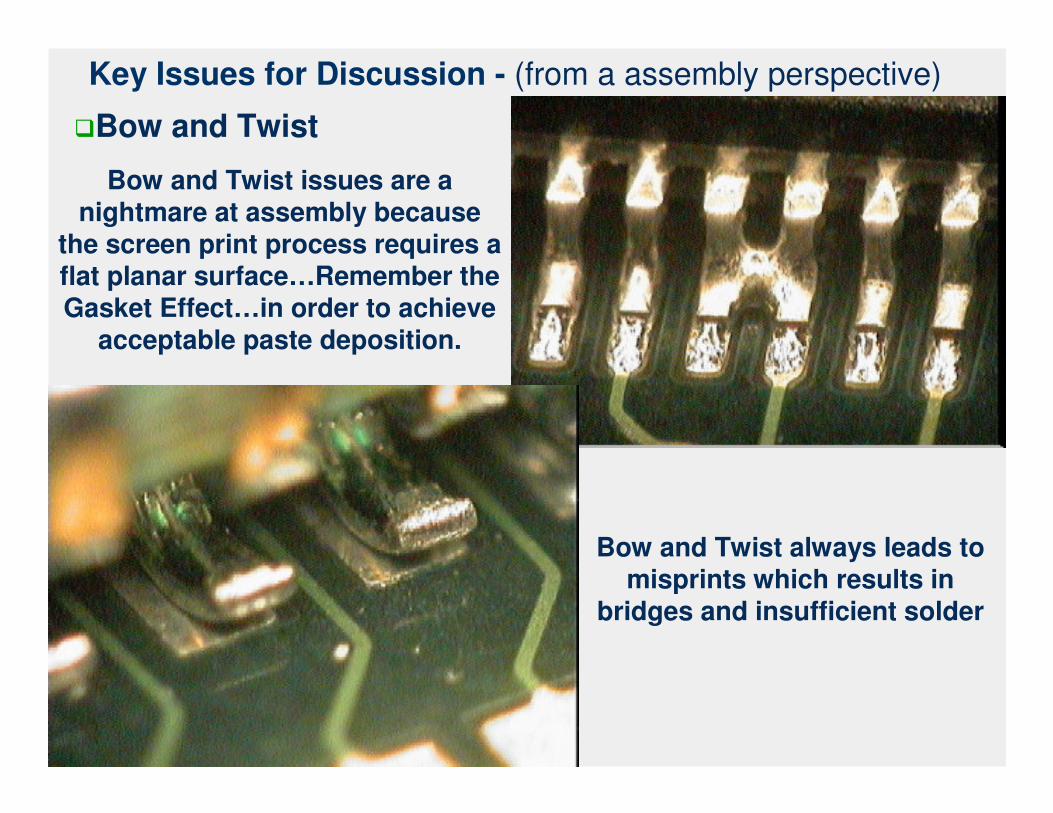
Key Issues for Discussion - (from a assembly perspective)
�Bow and Twist
Bow and Twist issues are a nightmare at assembly because
the screen print process requires a flat planar surface…Remember the Gasket Effect…in order to achieve
acceptable paste deposition.
Bow and Twist always leads to misprints which results in
bridges and insufficient solder
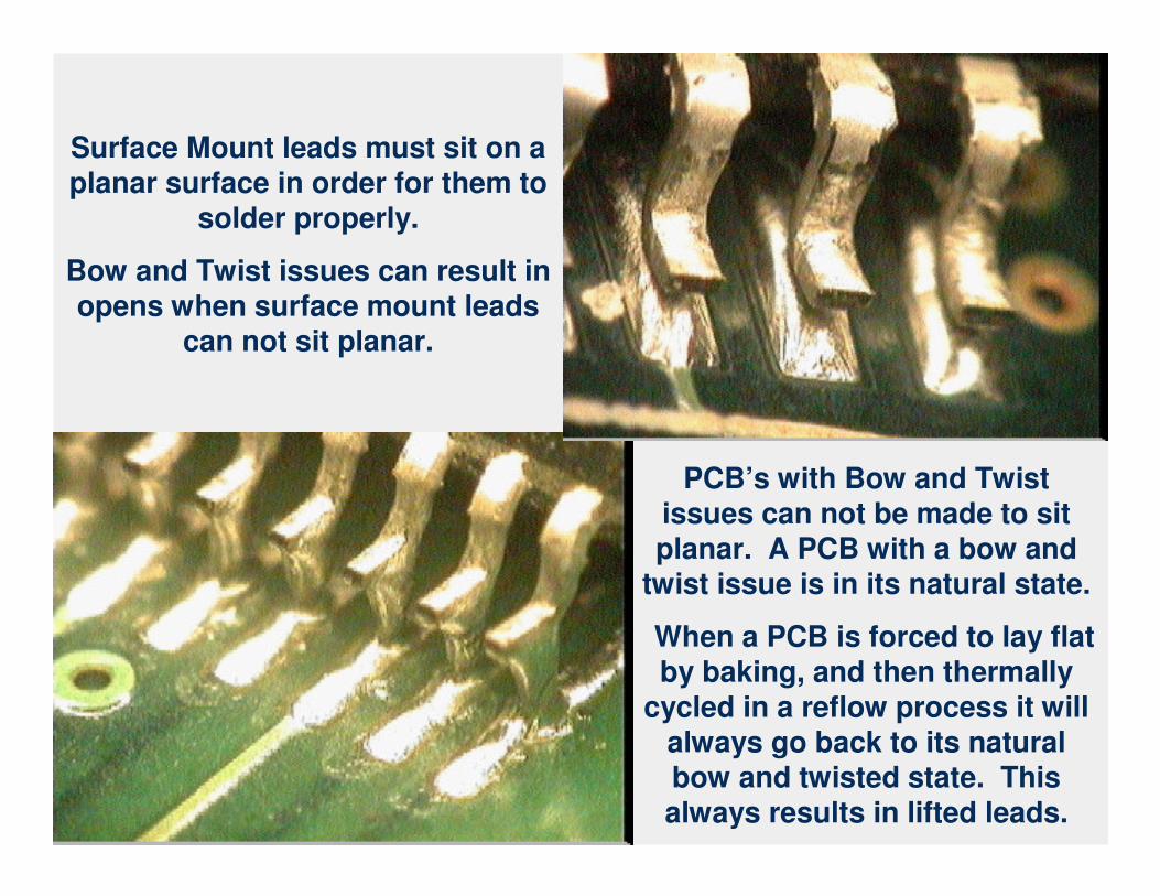
Surface Mount leads must sit on a planar surface in order for them to
solder properly.
Bow and Twist issues can result in opens when surface mount leads
can not sit planar.
PCB’s with Bow and Twist issues can not be made to sit planar. A PCB with a bow and
twist issue is in its natural state.
When a PCB is forced to lay flat by baking, and then thermally
cycled in a reflow process it will always go back to its natural bow and twisted state. This always results in lifted leads.

This PCB had a Bow and Twist issue that was
forced to lay planar, and when reflowed in a SMT
convection oven process the Via’s exploded
causing components to fly off the PCB.
A PCB with a Bow and Twist issue that is forced to lay flat can result in other issues during the SMT convection oven process.
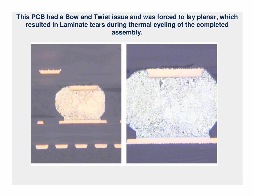
This PCB had a Bow and Twist issue and was forced to lay planar, which resulted in Laminate tears during thermal cycling of the completed
assembly.

� Non-Symmetrical Pads (nightmares at assembly; etch-defined pads; how to avoid issues at the design level)
etch-defined pad
Non-etch-defined padVs.
Mask Opening was made equal
Key Issues for Discussion - (from a assembly perspective)

Key Issues for Discussion - (from a designer’s perspective)
� Non-Symmetrical Pads (etch-defined pads)
Exposed Edge Defined

Key Issues for Discussion - (from a designer’s perspective)� Non-Symmetrical Pads (etch-defined pads)
Thermal Defined
Non-Thermal Defined

Mask Openings that are madeEqual for a non-etched defined pad Vs a etched defined pad will always
result in Non-Symmetrical Pads

Non-Symmetrical Surface Mount Chip Pads Always results in Tombstoning…
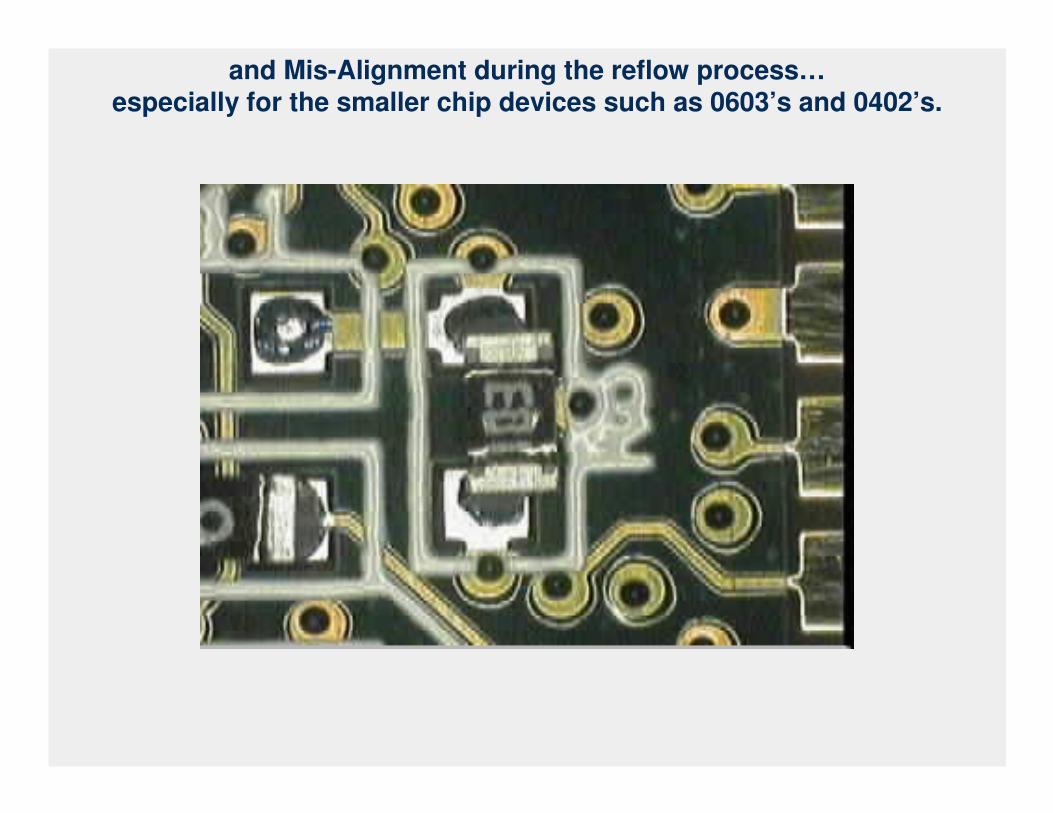
and Mis-Alignment during the reflow process…especially for the smaller chip devices such as 0603’s and 0402’s.

Key Issues for Discussion -(from a designer’s perspective)
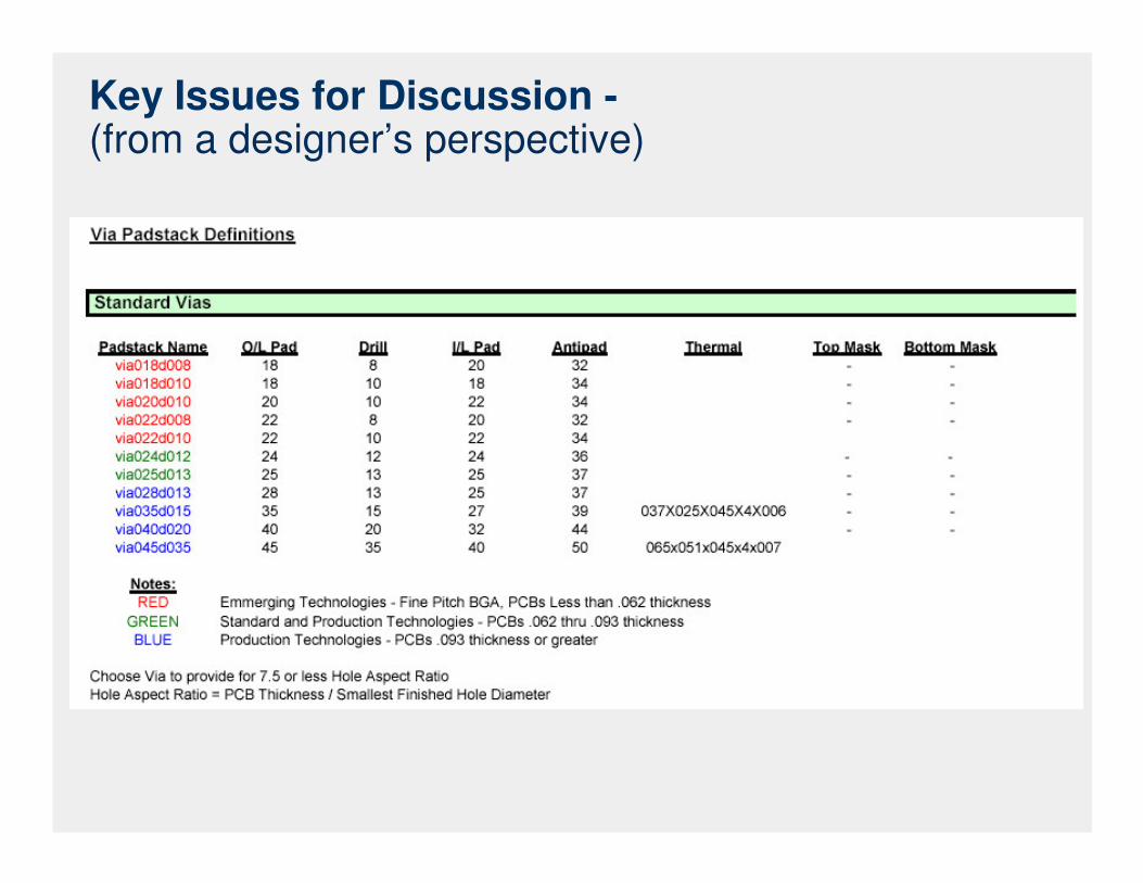
�Via – under – BGA
•Micro vias and print specifications
Key Issues for Discussion -(from a designer’s perspective)

Key Issues for Discussion -(from a designer’s perspective)

� Via – under – BGA (soldermask "via-capping" solutions; hole-plugging do’s and don’ts)
Key Issues for Discussion - (from a fabrication perspective)
Via Plugging Approaches ("Protected Vias" per IPC-SM-840C)
#1 #2 #3 Encroachment to Via Approach Encroachment to Via Approach PostPlugged Via Approach (aka, tentbust, rimless vias, gas holes) (For Test Point Access on Bottom Side) (aka, capped, plugged vias )
(Bottomside "Encroachment") (Via Plugging is 0 - 50% of the hole) (With ~95% of Vias on the Panel Plugged)
#4 #5PostPlugged Via Approach PrePlugged Via Approach
(For Test Point Access on Bottom Side) (Via Plugging is 80 - 100% of the hole)

Key Issues for Discussion - (from a assembly perspective)�Via – under – BGA (soldermask "via-capping"…Why it’s a must!)
Solder Paste Solder Spheres filling an unmasked via during the screen print process is unavoidable!
Photo at 150X mag
Solder Paste Solder Spheres fill an unmasked via during the screen print process.
Photo at 75X mag

When Solder Paste Solder Spheres fill an unmasked via
(during the screen print process) it results in Solder
Shorts to Non-Common Conductors.
Solder Shorts to Non-Common Conductors from solder paste
filling unmasked via’s is unavoidable!
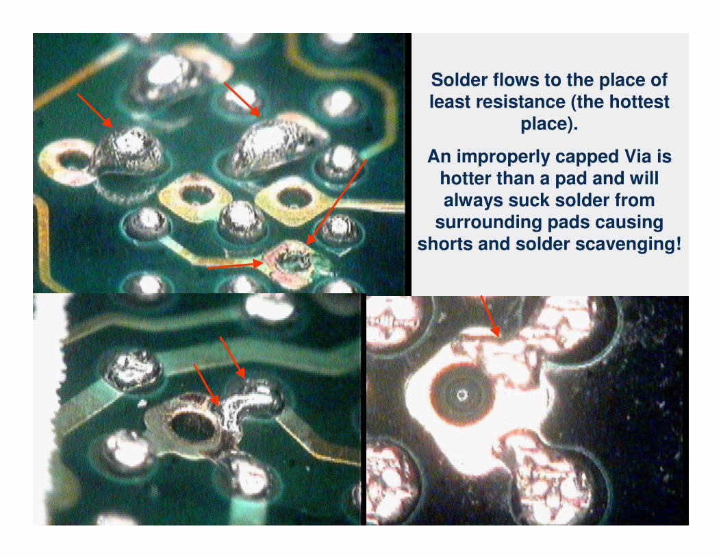
Solder flows to the place of least resistance (the hottest
place).
An improperly capped Via is hotter than a pad and will always suck solder from
surrounding pads causing shorts and solder scavenging!

Improper Capping of Via’s leads to out gassing of the solder
trapped in the Via during normal convection reflow processing.
Out gassing of solder will always result in shorts, opens,
insufficient, and solder splatter on gold fingers!
Key Issues for Discussion - (from a fabrication perspective)
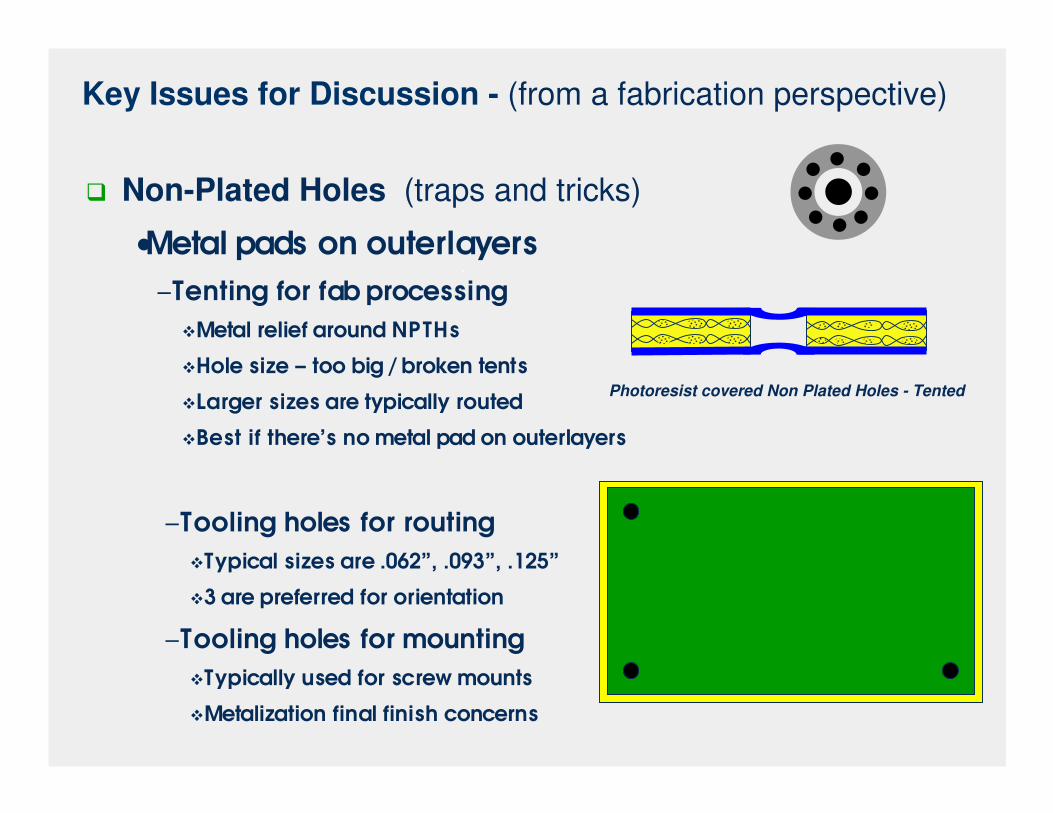
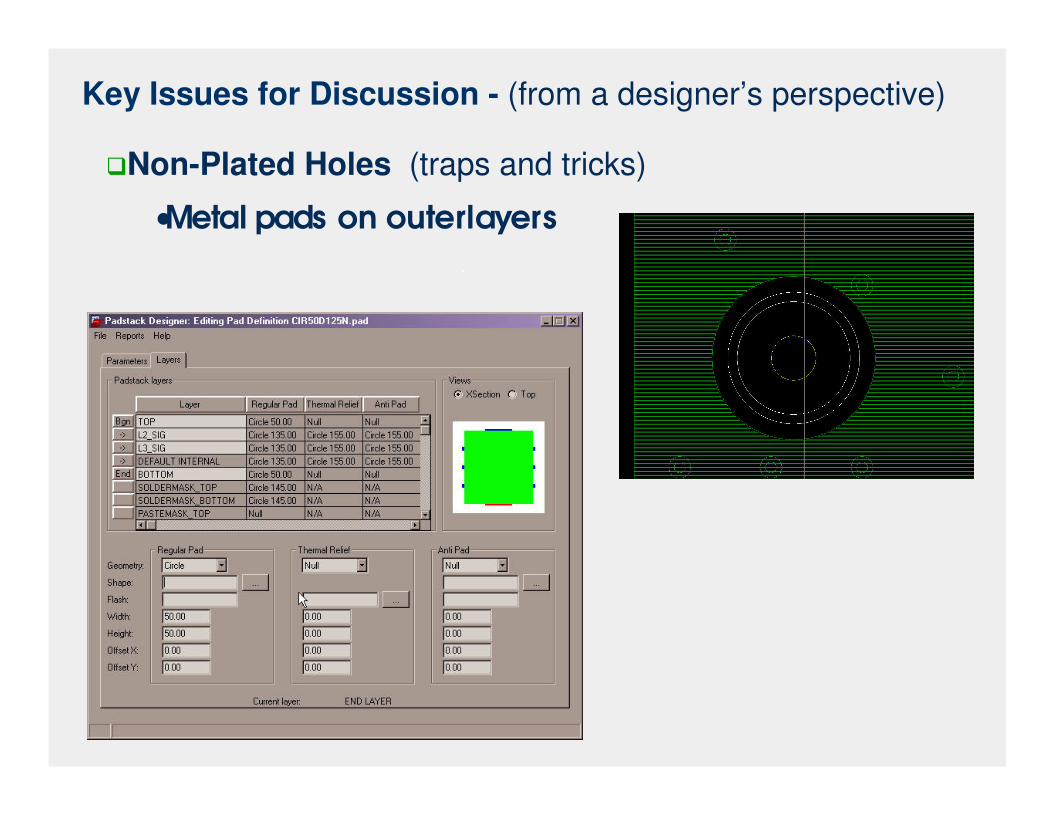
� Non-Plated Holes (traps and tricks)
•Metal pads on outerlayers–Tenting for fab processing
�Metal relief around NPTHs
�Hole size – too big / broken tents
�Larger sizes are typically routed
�Best if there’s no metal pad on outerlayers
–Tooling holes for routing�Typical sizes are .062”, .093”, .125”
�3 are preferred for orientation
–Tooling holes for mounting�Typically used for screw mounts
�Metalization final finish concerns
Photoresist covered Non Plated Holes - Tented
Key Issues for Discussion - (from a designer’s perspective)
�Non-Plated Holes (traps and tricks)
•Metal pads on outerlayers

Target Pad
Laser DrilledMicrovia Hole
Capture Pad
Mechanical Drilled Through Hole(Comparison)
Typical Geometry’sDrilled Hole Size - ~ .006” dia.Target Pad Size - ~ .012” dia.Capture Pad Size - ~ 80% the
solderball sizeAspect Ratio - < = .7 : 1
Typical Geometry’sDrilled Hole Size - ~ .010” dia.Pad Size - ~ .024” dia.
Aspect Ratio - < = 8.9 : 1
Key Issues for Discussion - (from a fabrication perspective)
� Vias (Aspect ratio challenges; pad size choices)

LAMINATE / DIMENSIONAL STABILITY
Before Lamination After Lamination (note Material Shrinkage)
Clearance
True Position
.0045
Rules Violation withNon Functional PadsRemoved
Pad Diameter
.005
.024
.036
.010Drill
Key Issues for Discussion - (from a fabrication perspective)
•Vias – Why do we need the larger pad sizes?
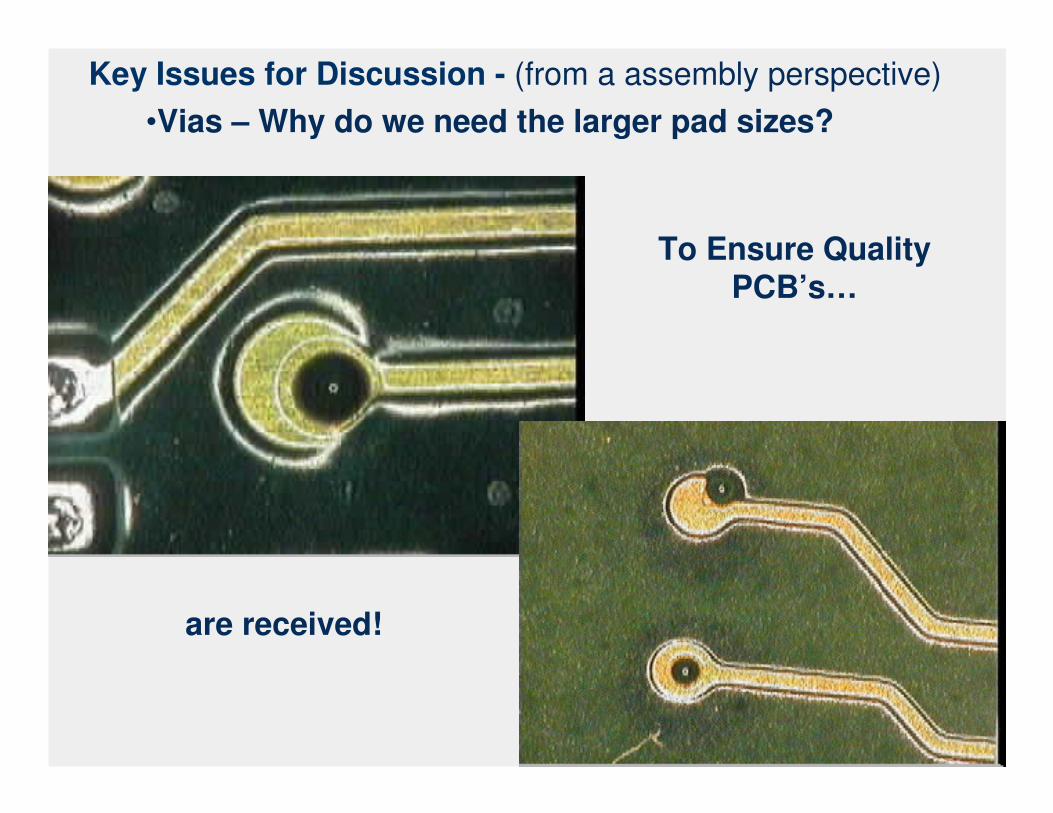
Key Issues for Discussion - (from a assembly perspective)•Vias – Why do we need the larger pad sizes?
To Ensure Quality PCB’s…
are received!

When Quality PCB’s are not received…
on time Delivery is nearly impossible!
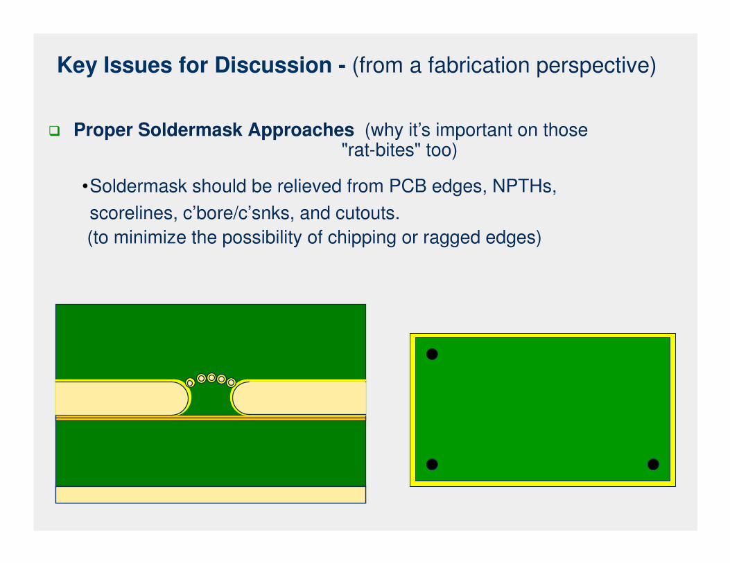
� Proper Soldermask Approaches (why it’s important on those "rat-bites" too)
•Soldermask should be relieved from PCB edges, NPTHs,scorelines, c’bore/c’snks, and cutouts. (to minimize the possibility of chipping or ragged edges)
Key Issues for Discussion - (from a fabrication perspective)
.100” Typical

Key Issues for Discussion - (from a designer’s perspective)
� Proper Array Dimensioning

Key Issues for Discussion - (from a designer’s perspective)
� Proper Array Dimensioning - Continued
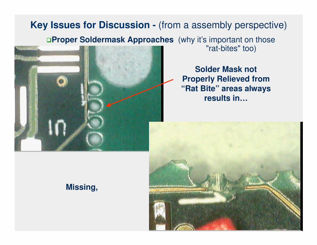
Key Issues for Discussion - (from a assembly perspective)�Proper Soldermask Approaches (why it’s important on those
"rat-bites" too)
Solder Mask not Properly Relieved from “Rat Bite” areas always
results in…
Missing,

Torn and…
Lifted Traces!

Soldermask not properly relieved from PCB edges, NPTHs, scorelines, c’bore/c’snks, and cutouts always results in
chipping or ragged edges!

Solder Mask should be sufficiently relieved around all pads, so as to allow for good mask Alignment. Especially BGA pads!

Solder mask that is not properly relieved can result in poor solder connections and CTE Issues take over.
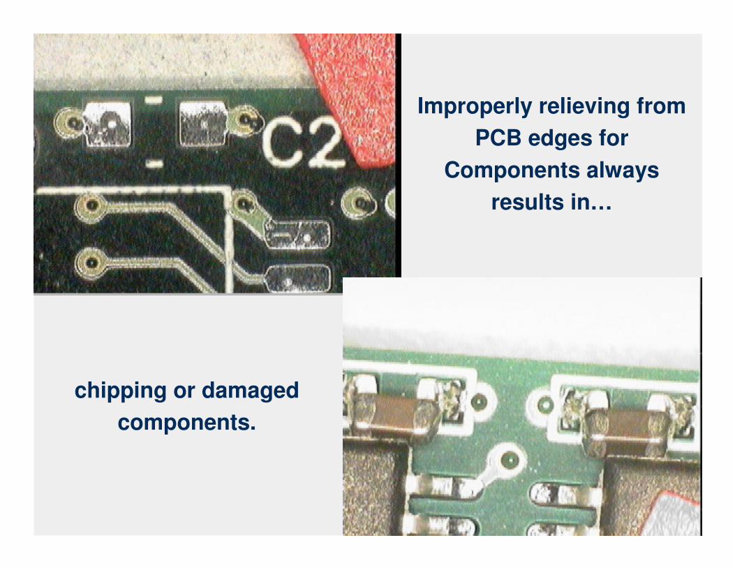
Improperly relieving from PCB edges for
Components always results in…
chipping or damaged components.

Improperly relieving from PCB edges for Via’s always results in damaged via’s.

Key Issues for Discussion - (from a fabrication perspective)
� Planes and thermals (how a little heat can make a fabricator soar)
Reasons not to use crosshatch thieving
Each small “sliver” ofphotoresist can redepositon the layer and cause anopen or a short (depending on where it lands).