ka-band wide-bandgap solid-state power amplifier: prototype … · ipn progress report 42-164...
TRANSCRIPT

IPN Progress Report 42-164 February 15, 2006
Ka-Band Wide-Bandgap Solid-State PowerAmplifier: Prototype CombinerSpurious Mode Suppression
and Power ConstraintsP. Khan1 and L. Epp1
Results of prototype hardware activities related to a 120-W, 32-GHz (Ka-band)solid-state power amplifier (SSPA) architecture study are presented. Spurious modesuppression and the power-handling capability of a prototype 24-way radial com-biner and a prototype 2-way septum binary combiner were investigated. Exper-imental data indicate that a commercial absorptive filter, designed to pass thecircular TE01 mode, effectively suppressed the higher-order modes generated bya narrowband, flower-petal-type mode transducer. However, the same filter wasnot effective in suppressing higher-order modes generated by the broadband Mariemode transducer that is used in the prototype waveguide radial combiner. Shouldgreater filtering be required by a particular SSPA application, a broadband modefilter that can suppress specifically those higher-order modes that are generated bythe Marie transducer will need to be developed. A back-to-back configuration of theprototype radial combiner was tested with drive power up to approximately 50 W.No anomalous behavior was observed. Power measurements of the septum combinerindicate that up to 10-W radio frequency (RF) can be dissipated in the integratedresistive element before a permanent performance shift is observed. Thus, a givenadder (a single-stage, 2-way combiner) can safely combine two 20-W sources, andthe adder will not be damaged in the event of a source failure. This result is usedto calculate the maximum source power that can be safely combined as a functionof the number of sources combined and the number of source failures allowed in amulti-stage combiner. The analysis shows that SSPA power >140 W can be gen-erated by power combining 16 sources producing 10 W each. In this configuration,up to three sources could fail with the guarantee that the combiner would not bedamaged. Finally, a modified prototype septum combiner design was verified. Theimproved design reduced the assembly time from over 2 hours to about 15 minutesper adder.
1 Communications Ground Systems Section.
This research was carried out at the Jet Propulsion Laboratory, California Institute of Technology, and was sponsoredby Glenn Research Center, and the National Aeronautics and Space Administration. Reference herein to any specificcommercial product, process, or service by trade name, trademark, manufacturer or otherwise, does not constitute or implyits endorsement by the United States Government or the Jet Propulsion Laboratory, California Institute of Technology.
1

I. Introduction
A. Wide-Bandgap Solid-State Power Amplifier Architecture Study
Recent advances in wide-bandgap (WBG), gallium nitride (GaN) semiconductor technology may enablethe development of efficient solid-state power amplifiers (SSPAs) as an alternative to the traveling-wavetube amplifier (TWTA) for space applications. Key goals of the current effort are to assess the technicalfeasibility of such an SSPA for operation at 32 GHz (Ka-band), estimate the required WBG deviceperformance, and generate a roadmap to an engineering model of the SSPA.
During the initial phase of this work, we investigated power-combining technologies and SSPA archi-tectures that can enable a 120-W, 40 percent power-added efficiency (PAE) SSPA to be developed foroperation over a 31- to 36-GHz band [1–4]. The study proposed three candidate architectures for thetarget SSPA. The proposed architectures are based on a waveguide radial combiner,2 a septum binarycombiner,3 and a parallel-plate radial combiner.4 Subsequently, a prototype 24-way waveguide radial com-biner and a prototype 2-way septum combiner were designed and fabricated to validate key performanceparameters. Both prototype combiners demonstrated excellent port match and insertion loss character-istics over the required frequency band [4]. The measurements validated important RF parameters thatdirectly affect the efficiency of the SSPA and that help establish WBG device requirements.
This article documents the results of follow-on activities to better understand the operation andperformance limitations of the prototype waveguide radial and septum binary combiners.
B. Follow-On Activities
Follow-on activities relating to the waveguide radial combiner included measurements pertaining tospurious mode effects and high-power operation. The radial combiner employs a waveguide mode trans-ducer to generate a circularly symmetric field distribution at the power-combining junction of the circuit.The transducer contains overmoded sections in which spurious modes can be excited and trapped. Thesetrapped modes are believed to generate observed spikes in the transfer characteristics of the combiner.The measured insertion loss of the prototype combiner, including the effect of the spurious modes, poten-tially can meet target SSPA requirements. However, elimination of the spurious modes can significantlyimprove the combining efficiency. Moreover, system-level implications of these spurious modes have yet tobe determined. Therefore, we investigated an approach to suppress trapped modes. The effectiveness ofa commercial mode filter to suppress trapped modes was measured for both a commercial, narrowband,flower-petal mode transducer and the broadband Marie transducer specifically designed for the targetapplication. For the high-power test, a back-to-back configuration of a 24-way radial combiner prototypewas tested with drive power up to 50 W.
Follow-on activities relating to the septum binary combiner included high-power tests and designimprovements for manufacturability. The septum combiner’s thin-film resistive element is critical toachieving the excellent small-signal radio frequency (RF) performance previously demonstrated. The re-sistive element’s ability to dissipate heat, however, is an important point of interest. For the high-powertest, a prototype 2-way combiner was driven with an asymmetric, large-signal excitation to measure themaximum power that can be safely dissipated by the resistive element. To improve the mechanical design,
2 L. W. Epp, A. R. Khan, D. J. Hoppe, and D. Kelley, Wideband 24-Way Radial Power Combiner/Divider Fed by a MarieTransducer, JPL New Technology Report no. 41511 (internal document), Jet Propulsion Laboratory, Pasadena, California,December 7, 2004.
3 A. R. Khan, L. W. Epp, D. J. Hoppe, and D. Kelley, Thin-Film Resistive Septum Waveguide Power Combiner, JPL NewTechnology Report no. 40903 (internal document), Jet Propulsion Laboratory, Pasadena, California, November 16, 2004.
4 A. R. Khan, L. W. Epp, and D. J. Hoppe, Wideband (31 to 36 GHz) Parallel Plate Power Combiner/Divider withIsolation, JPL New Technology Report no. 41758 (internal document), Jet Propulsion Laboratory, Pasadena, California,January 31, 2005.
2

a new method of integrating the resistive element with the waveguide structure was validated. The newdesign decreases the number of substrates that must be separately assembled and significantly reducesthe time required to fabricate the septum combiner.
II. Waveguide Radial Combiner Activities
A. Circular Taper Transitions for the Mode Filter
The effectiveness of a commercial circular waveguide mode filter [5] to suppress spurious modes in theprototype waveguide combiner was measured. The mode filter is designed to propagate the desired TE01
circular mode and attenuate higher-order spurious modes. A set of linear tapers was manufactured toallow the filter to be inserted between the mode transducer and the power combiner radial base [Fig. 1(a)].
Since the waveguide diameter of the filter and combiner differ by only 0.33 mm, a short, 2.5-cm taperlength is sufficient to achieve excellent match. To verify this, a 10-section, stepped-taper model of thetransition was analyzed using a commercial mode-matching analysis tool [Fig. 1(b)]. The theoreticalmatch is >57 dB, and the theoretical insertion loss is essentially 0 dB over the design band of 31 to36 GHz. The analysis also indicates that the desired TE01 mode does not couple effectively to higher-order modes and, thus, the taper is not expected to directly generate additional mode impurity.
B. Flower-Petal Transducer Spurious Mode Suppression
In addition to enabling filter measurements, the taper transitions allowed the prototype radial combinerbase to be fed by a commercial mode transducer [6]. The transducer design is a “flower-petal” type,described by Hoag et al. [7]. The flower-petal transducer was measured to operate over the 33.5- to35.5-GHz band. Although the bandwidth does not meet the target SSPA requirements, tests were carriedout nonetheless to gain insight into the operation of the combiner base and the mode filter. It shouldbe noted that the mode filter used in our measurements was designed to work in conjunction with thisspecific flower-petal transducer design. The transducer and filter were both designed to operate at a34.5-GHz center frequency.
To verify that the filter effectively suppresses spurious modes, two flower-petal transducers were mea-sured in a back-to-back configuration. Two measurements were taken, one with and one without themode filter inserted between the transducers (Fig. 2). It is clear that the filter is effective in suppressingthe spurious spikes occurring at 34.2 and 35.0 GHz in the response of the flower-petal transducer. It isalso evident that a single filter inserted between the transducers adds approximately 0.1 dB of additionalinsertion loss.
Next, two radial bases, each fed by a flower-petal transducer, were measured in a back-to-back config-uration. Two measurements were taken, one with and one without a mode filter inserted between eachtransducer and its radial base (Fig. 3). A photograph of the setup without filters is shown in Fig. 4. Asin the back-to-back transducer case discussed above, the filters are effective in suppressing the spuriousspikes in the transfer characteristics of back-to-back radial combiners fed by flower-petal transducers.Over the 33.5- to 35.5-GHz band, the worst-case insertion loss of back-to-back combiners without a filteris measured to be 2.1 dB. With a filter, the worst-case insertion loss is 0.5 dB. The spikes are reduced inmagnitude from about 1.75 dB to about 0.2 dB. Based on this measurement, the insertion loss of a singleradial combiner is estimated to be 0.25 dB, including the mode transducer and filter.
C. Marie Transducer Spurious Mode Suppression
A set of measurements was performed to determine the effectiveness of a mode filter to suppress spu-rious mode effects in the radial combiner fed by the Marie transducer. The measurements correspondto those done for the flower-petal transducer, as discussed in Section II.B. The same mode filters and
3

FREQUENCY, GHz
31.0 31.5 32.0 32.5 33.0 33.5 34.0 34.5 35.0 35.5 36.0
S11
,S21
(T
E01
, TE
01),
dB
−80
−70
−60
−50
−40
−30
−20
−10
0
S11
S2110-SECTIONLINEAR TAPER
D 2
L
D 11.610 cm
2.54 cm
1.643 cm
Fig. 1. Geometry showing how the mode filter was adapted to the modetransducer: (a) a pair of taper transitions was used to insert a modefilter between the mode transducer and the combiner base and(b) analysis of a single waveguide taper.
(b)
CombinerInputs
RadialCombiner
BaseCombiner
Output
Pair of CircularWaveguide Tapers withAppropriate Flanges
ModeTransducer
X
Y
S
ModeFilter
(a)
4

33.5 34.0 34.5 35.0 35.5
1 12 2
NO FILTER
NO FILTER
WITH FILTER
WITH FILTER−4.0
−3.5
−3.0
−2.5
−2.0
−1.5
−1.0
−0.5
0.0
FREQUENCY, GHz
MA
GN
ITU
DE
(S
21),
dB
Fig. 2. Back-to-back flower-petal transducers measured withand without a mode filter.
33.5 34.0 34.5 35.0 35.5
1 12 2
NO FILTERS
NO FILTERS
WITH FILTERS
WITH FILTERS
−0.2
−0.4
−0.6
−0.8
−1.0
−1.2
−1.4
−1.6
−1.8
−2.0
−2.2
0.0
FREQUENCY, GHz
MA
GN
ITU
DE
(S
21),
dB
Fig. 3. Back-to-back radial bases fed by flower-petal transducers,measured with and without mode filters.
5

Waveguide bends connecting
24 combiner input ports of the
first base to those of the second.
Back-to-back radial bases
Seen edge-on
Flower-petal
mode transducer
Waveguide bends connecting
24 combiner input ports of the
first base to those of the second.
Back-to-back radial bases
Seen edge-on
Flower-petal
mode transducerFlower-Petal
Mode TransducerBack-to-Back Radial
Bases Seen Edge-On
Waveguide Bends Connecting24 Combiner Input Ports of the
First Base to Those of the Second
Fig. 4. Photograph of the measurement setup corresponding to Fig. 3,the no-mode-filter case.
radial bases were used in both sets of measurements. Although the Marie transducer operates over thefull 31- to 36-GHz band, measurements were limited by the mode filter design to the 33.5- to 35.5-GHzband.
As with the flower-petal transducer, two Marie transducers were measured in a back-to-back config-uration with and without the mode filter inserted between the transducers (Fig. 1). Unfortunately, theresponses with and without the filter do not appear to be significantly different. Referring back to Fig. 2,it is evident that the mode filter suppressed certain large spurious spikes in the response. However,smaller (∼0.1 dB) spikes were not affected. Furthermore, the filter seemed to introduce additional small(<0.1 dB) spikes in the response. Thus, clearly the mode filter, an absorptive helix design, suppressescertain spurious modes and not others. It appears that, in the measured band, back-to-back Marietransducers do not generate significant power in modes for which this specific filter design is effective.
The filtered response in Fig. 5 can be offset by 0.1 dB (the loss of the mode filter) such that the tworesponses superimpose (Fig. 6). Measured data, thus plotted, seem to indicate that some small spikesgenerated by the transducers were suppressed by the mode filter.
The transducer response outside the filter operating band contains spikes as large as 0.4 dB (Fig. 7).Measured results suggest that, to suppress these spikes, a new mode filter should be designed thatoperates not only over the required frequency band of 31 to 36 GHz, but which suppresses spuriousmodes specifically generated by the Marie transducers.
6

33.5 34.0 34.5 35.0 35.5
1 2 1 2
NO FILTER
NO FILTER
WITH FILTER
WITH FILTER
−0.1
−0.2
−0.3
−0.4
−0.5
−0.6
−0.7
−0.8
0.0
FREQUENCY, GHz
MA
GN
ITU
DE
(S
21),
dB
Fig. 5. Back-to-back Marie transducers, measured with and without a mode filter.
33.5 34.0 34.5 35.0 35.5
−0.10
−0.15
−0.20
−0.25
−0.30
−0.35
−0.40
−0.45
−0.50
FREQUENCY, GHz
MA
GN
ITU
DE
(S
21),
dB
Fig. 6. Data from Fig. 5, with the filtered case offset and the vertical scale expanded. A small amount of power seems to be generated in modes for which the filter is effective.
SPIKES IN UNFILTERED RESPONSE
FILTERED RESPONSE
7

31.0 33.032.0 34.0 35.0 36.0
−1.4
−1.2
−1.0
−0.8
−0.6
−0.4
−0.2
0.0
−1.6
−1.8
−2.0
FREQUENCY, GHz
MA
GN
ITU
DE
(S
21),
dB
Fig. 7. Back-to-back radial bases fed by Marie transducers.
WITH FILTER
WITH FILTER
NO FILTER
NO FILTER
FILTER BAND
1 2 1 2
D. Radial Combiner High-Power Test
The back-to-back configuration of the 24-way radial combiner, fed by the Marie transducer, was testedunder high-power excitation at 34.4 GHz (Fig. 8). Measured input and output powers are listed in Table 1.
The prototype radial combiner is purely a waveguide structure with no resistive elements. As such, thepower-handling capability of the prototype combiner is expected to be limited by waveguide breakdownonly. Due to limitations of the measurement setup, however, the combiner was tested with drive powerup to approximately 50 W. Since this level of drive is below the expected limits, anomalous combinerbehavior was neither expected nor observed. If a mode filter is used, the power capability of the radialcombiner will likely be limited by the power limits of the mode filter.
III. Septum Combiner Activities
A. Septum Combiner High-Power Test
The power-handling capability of the septum combiner is limited by the amount of power that canbe dissipated in the septum resistive element without causing damage. Under equal excitation of thecombiner input ports (port 1, port 2), very little power is dissipated in the resistive element. The worst-case insertion loss of the combiner is <0.1 dB. Thus, if each input port is excited with 1 W, the totalpower loss is <46 mW. A fraction of this lost power is dissipated in the resistive element. The remainingpower is lost due to port mismatch and finite conductor loss. However, if only one input port is excitedwhile the other is not, approximately half of the drive power is delivered to the output port and the otherhalf is dissipated in the resistive element. Such asymmetry in excitation can arise in a power-combiningapplication due to one or more source failures.
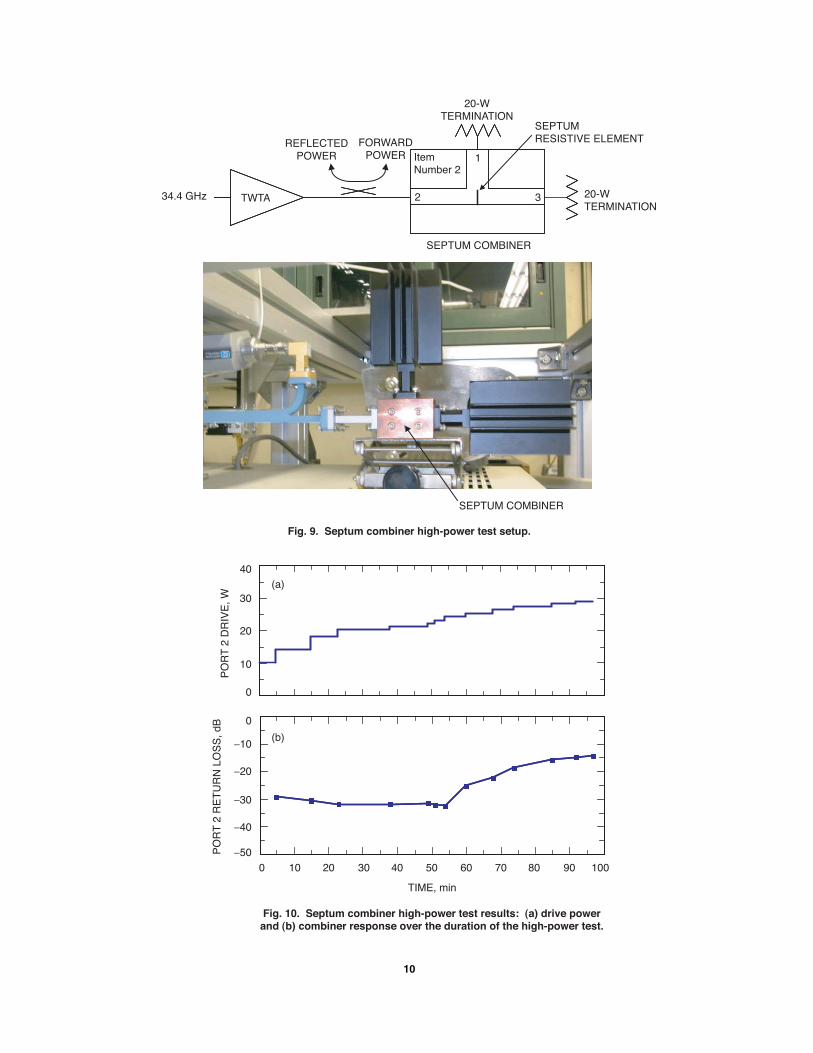
To determine how much power can be safely dissipated in the septum resistive element, a prototypecombiner was tested with high-power excitation. The experimental setup is illustrated in Fig. 9. ATWTA amplifier was used as a high-power source to excite only one input port of the combiner, port 2.The match at port 2 was monitored as a function of drive level. The input match is a strong function ofthe sheet resistance of the resistive element and is, therefore, a good indicator of changes resulting fromthe power load.
8

INPUT
34.4GHz
TWTA
BACK-TO-BACKRADIAL COMBINER
OUTPUT
HIGH-POWERTERMINATION
Fig. 8. Measurement setup for radial combiner high-power test.
Table 1. 24-way radial combiner measuredinput and output powers.
Input power, W Output power, W
12.15 10.0
18.1 15.0
23.6 20.0
29.4 25.0
35.3 30.0
41.5 35.0
47.7 40.0
Figure 10 illustrates the drive profile and the corresponding response of the prototype combiner as afunction of test time. Starting at an initial excitation of 10 W, the drive power was increased in stepsuntil significant degradation in return loss was observed. Each increase in drive power generally wasfollowed by a 5-minute dwell period to allow the system to reach thermal equilibrium. Return loss datapoints were taken at the end of each dwell period. The initial improvement in return loss, with increasingdrive power up to 23 W, could be due to a shift in the resistive element’s sheet resistance. However,information from prior test runs suggests that the shift likely is due to instrumentation. Termination ofthe test below 23 W indicates the shift in combiner performance is not permanent. Moreover, as shownin Fig. 10, the return loss is stable for a 20-W drive, over a 15-minute dwell time. Increasing the drivebeyond 23 W, however, results in a gradual degradation of performance. Unlike the performance shiftbelow 23 W, this degradation mode appears to result in a permanent change in performance.
The degradation of return loss, as drive power is increased from 23 W to 29 W, seems to saturate. Thereare two possible explanations. First, with each unit increase in drive power, as the return loss degrades,a greater fraction of power is reflected and a lesser fraction is dissipated in the resistive element. Second,as return loss degrades, performance of the circuit becomes less sensitive to the value of the resistiveelement’s sheet resistance. Both effects seem to prevent a “runaway” situation and make the mode ofcombiner degradation gradual and self-limiting. This behavior should contribute to the desired gracefuldegradation characteristic of the target SSPA.
A more accurate, small-signal measurement of the prototype combiner was taken before and after thehigh-power test (Fig. 11). The output port match (S11) does not depend on the septum sheet resistanceand, thus, remained unchanged, as expected.
The input port match (S22, S33) and isolation (S32), however, degraded to approximately 16 dB.The observed degradation is believed to result from an increase in the tantalum nitride (TaN) film
9
34.4 GHz TWTA
REFLECTEDPOWER
FORWARDPOWER
20-WTERMINATION
20-WTERMINATION
SEPTUMRESISTIVE ELEMENT
SEPTUM COMBINER
1
2 3
ItemNumber 2
SEPTUM COMBINER
Fig. 9. Septum combiner high-power test setup.
0 10 20 30 40 50 60 70 80 90 100
TIME, min
−50
−40
−30
−20
−10
0
0
10
20
30
40
PO
RT
2 R
ET
UR
N L
OS
S, d
BP
OR
T 2
DR
IVE
, W
Fig. 10. Septum combiner high-power test results: (a) drive power and (b) combiner response over the duration of the high-power test.
(a)
(b)
10

12
3
12
3
12
3
1
33
21
X Y
Z
−2.8
−2.9
−3.0
−3.1
−3.2
−3.3
|S|,
dB
0
−5
−10
−15
−20
−25
−30
−35
−40
|S|,
dB
0
31 32 33 34 35 36
−10
−20
−30
−40
−50
−60
−70
|S|,
dB
FREQUENCY, GHz
31 32 33 34 35 36
FREQUENCY, GHz
31 32 33 34 35 36
FREQUENCY, GHz
S22, S33 After
S22, S33 Before
S11 After
S11 Before
S32 AfterS21 After
Item Number 2
S31 After
S32 Before
S21 Before
S31 Before
Fig. 11. Comparison of small-signal measurements before and after the high-power test: (a) geometry of the septum combiner being tested, (b) port match, (c) coupling, and (d) isolation.
(a) (b)
(c) (d)
sheet resistance due to RF heating. An increase in the thickness of the surface oxide layer is a possiblemechanism for the change in sheet resistance.
To determine the value of sheet resistance after the high-power test, the value of sheet resistance inthe original simulation model was modified until a good match between analysis and measurement wasobtained (Fig. 12). The sheet resistance in the model needed to be increased from 128 Ω/sq. (beforethe high-power test) to 415 Ω/sq. (after the high-power test). This significant, 224 percent increase isconsistent with prior observation that the combiner circuit is well-tolerant to variations in the septumsheet resistance. For manufacturing the prototype combiner, the standard ±10 percent tolerance in sheetresistance was found to be sufficient for achieving the design performance. As part of future activities,it should be possible to measure the magnitude and distribution of the modified sheet resistance in theresistive element under test and compare them directly with analysis. The resulting data could be usedto optimize the thermal design of the resistive element, if needed.
B. Septum Combiner Architecture Power Constraints
A 2-way septum combiner (adder) can be cascaded in a binary fashion to implement an N -way com-biner, where N is constrained to a power of 2. The 8-way combiner case (N = 8) is illustrated in Fig. 13.In general, for an N -way combiner, there are (N − 1) identical adders. To ensure the resistive elementin no single adder exceeds its power rating, the source powers must be appropriately limited. Based onmeasurements of the prototype adder, we can estimate the power constraints for a general N -way septumcombiner, as discussed below.
11

12
3
12
3
12
3
12
3
2
3
1
Z
S32 MeasurementS32 Analysis
YX
S31 Measurement
S21 Measurement
S21, S12 Analysis S31, S13 Analysis
S11 Measurement
S11 Analysis
S22, S33 AnalysisS22, S33 Measurement
−2.98
−3.00
−3.02
−3.04
−3.06
−3.08
MA
GN
ITU
DE
|S|,
dB
0
−5
−10
−15
−20
−25
−30
−35
−40
MA
GN
ITU
DE
|S|,
dB
31 32 33 34 35 36
FREQUENCY, GHz
31 32 33 34 35 36
FREQUENCY, GHz
−10
−20
−30
−40
−50
−60
MA
GN
ITU
DE
|S|,
dB
31 32 33 34 35 36
FREQUENCY, GHz
(a) (b)
(d)(c)
Fig. 12. Comparison of analysis, with the septum sheet resistance modified from the original design and small-signal measurements taken after the high-power test: (a) geometry of the septum combiner being tested, (b) port match, (c) coupling, and (d) isolation.
N SourcesDeliveringP Eachsrc
N = 8
S8
S7
S6
S5
S4
S3
S2
S1
Stage 1 Stage 2 Stage 3
a4
a6
a5
a7
a3
a2
a1
N − 1 Identical Adders
Output = N * Psrc
Fig. 13. General layout of an 8-way binary combiner.
12

Results of the high-power test indicate that a drive imbalance, or differential input (Pinput1 −Pinput2),of up to approximately 20 W can be tolerated by an adder (Section III.A). Since nearly half of this poweris dissipated in the septum resistive element, the maximum power that can be safely dissipated in theresistive element of a given adder is 10 W.
For symmetric excitation, small-signal measurements indicate the insertion loss of the adder is <0.1 dB(Fig. 12). A fraction of this lost power is dissipated in the resistive element. The remainder is lost dueto port mismatch and finite conductor loss. Making the conservative assumption that all lost power isdissipated in the resistive element, we note that, for symmetric excitation, up to 5 percent of the powerat each input port of a given adder is dissipated in its resistive element. Thus, in theory, a given addercan combine two sources producing 200 W (=10 W/0.05) each, provided the source powers are equal atall time. The maximum combined output possible in this theoretical case is, therefore, 400 W.
To ensure the root adder in the final stage of an N -way binary combiner does not exceed this limit,the source power must be limited to the following. Constraint 1:
Psrc ≤ 400N · (Ls)ns
watts (1)
where
Psrc = source power at each input
N = number of sources combined
ns = number of stages = log2(N)
Ls = average insertion loss per stage
Constraint 1 ensures that the power limit of the root adder will not be exceeded under normal, symmetricoperation (i.e., with no source failures). Adders at earlier stages dissipate successively lower power.
Asymmetric drive resulting from source failures, however, potentially can damage adders at any stageof the binary tree. The specific adder expected to be damaged depends on the source power, the numberof source failures, and the failure distribution. If the combiner is required to withstand these failureswithout damage, the source power must be further limited. We note that a given adder experiencesmaximum drive asymmetry when all sources feeding one input branch fail while all sources feeding theother branch produce full power. The probability of this failure distribution decreases with an increasingnumber of failures under consideration. However, to be conservative, we will assume this worst-casefailure distribution for the following analysis.
Constraint 1 allows Psrc to exceed 20 W (i.e., for N ≤ 16). However, with Psrc > 20 W, a first-stageadder can be damaged if one of its two sources fails. Thus, to tolerate at most one failure, Psrc cannotexceed 20 W. For two source failures, the maximum drive asymmetry of 2Psrc is experienced by a second-stage adder. Thus, to tolerate at most two failures, Psrc cannot exceed 10 W. The case of three failuresdoes not increase the magnitude of asymmetry in the system as compared with two failures. In general,for an N -way combiner, the maximum asymmetry is experienced by the root adder when N/2 sourceson one half of the binary tree fail. Additional failures in the other half of the tree actually decreaseasymmetry. Thus, for guaranteed immunity against an arbitrary number of failures, the source powercannot exceed 20/(N/2) = 40/N W.
In general, to ensure the resistive element in no single adder exceeds its power rating, the followingconstraint must be observed in addition to constraint 1. Constraint 2:
13

Psrc ≤ 20nf · (Ls)nsf
watts, nf = 2, 4, 8 · · · N
2(2)
Psrc ≤ 40N · (Ls)nsf
watts,N
2< nf ≤ N (3)
where
Psrc = source power at each input
N = number of sources combined
nf = maximum number of source failures allowed
nsf = log2(nf ), the number of stages between the source and power limiting adder
Ls = average insertion loss per stage
The maximum source and output power for various N and nf are tabulated in Table 2. For a 140-WSSPA, a 16-way combiner (N = 16) could be used to power combine 10-W sources. According to Table 2,up to three such sources can fail without overloading any resistive element in the combiner. Alternatively,a 32-way combiner (N = 32) can be used to power combine 5-W sources. For this configuration, up toseven sources can fail without overloading any resistive element.
Assuming the source failures are independent, the probability of nf failures is equal to the probabil-ity of a single failure raised to the power nf . The worst-case scenario of nf failures, therefore, quickly
Table 2. Maximum source power and maximum combined outputpower for guaranteed safe operation, as a function of number ofsources combined (N) and the maximum number of source failuresallowed (nf ).
N nf Psrc max, W Pout max, W
2 1 20.0 39
4 1 20.0 76
2–3 10.3 39
8 1 20.0 147
2–3 10.3 76
16 1 20.0 287
2–3 10.3 147
32 1 14.4 400
2–3 10.3 287
4–7 5.3 147
Note: Calculation assumes Ls = 0.12 dB average loss per com-biner stage; Pout max is the maximum SSPA output with no sourcefailure.
14

becomes highly improbable as nf increases. It seems unlikely that a real system will be designed with anexpectation of greater than at most three failures. Therefore, depending on the source power available,either a 16-way or a 32-way combiner could be used to implement the target SSPA and guarantee safeoperation in the event of multiple source failures.
C. Improved Design for Manufacturability
The prototype septum combiner fabricated during the initial phase of this study employed split-blockfabrication in which the top and bottom halves of the waveguide blocks were fabricated separately. Theresistive septum in this original design also was implemented in two halves. A pair of alumina substrateswith the TaN resistive sheet in between (forming the bottom half of the septum) was integrated withthe bottom waveguide block [Fig. 14(a)]. An identical pair of substrates forming the top half of theseptum was integrated with the top waveguide block. This approach allows the septum substrates to beintegrated with waveguide blocks before the waveguide blocks are mated [Fig. 14(b)].
A benefit of the original design is that disruptions in the waveguide wall (e.g., due to slots) areminimized. This simplifies the electrical design and increases the likelihood that the fabricated part willmore closely reproduce the designed performance. A drawback, however, is that great care is needed tointegrate the septum with the waveguide. Not only must two sets of substrates be integrated with thewaveguide blocks, the substrates must be fixed to the metal structure with careful application of epoxyor silicone room temperature vulcanising (RTV). This greatly increases the assembly time.
a eded
Pair of SubstratesIntegrated with BottomWaveguide Block
(a) (b)
(c) (d)
Blocks Shown Partially Mated
Remove Cover PlateEdge of SubstratesVisible Through Slot inWaveguide Wall
Fig. 14. The prototype septum combiner. (a) and (b): the original, split-card method of integrating the septum. Two substrate pairs (one pair forming the upper and one pair forming the lower half of the septum) are separately integrated with each waveguide block before the blocks are mated. (c) and (d): the new, improved, slot-insertion method of integrating the septum. A single substrate pair (forming the full septum) is inserted through a slot on the waveguide wall after the waveguide blocks are mated.
15

A new design was implemented that addresses the manufacturing issues. In the new design, thewaveguide structure is manufactured as in the original design, i.e., as split-blocks. However, the blocksare mated first without the septum substrates. A single pair of substrates (forming the full septum) thenis inserted through a slot in the narrow wall of the waveguide structure [Figs. 14(c) and 14(d)]. Thestructure is designed such that the substrates are held captive by the waveguide metal. The use of epoxywithin the waveguide therefore is not required. A cover plate, illustrated in Fig. 14(d), is used to cap theslot. Although the structure does not require that epoxy be used, it may be prudent to do so for increasedthermal conductivity and to eliminate small performance variations that may result from potential cardmovements. The epoxy, however, need not be applied with the care required in the original design. Inthe new design, since the epoxy can be placed in the slots, outside the waveguide volume, the epoxy doesnot interact effectively with electromagnetic fields.
The new design reduces the individual substrate count from 4 to 2 per adder and decreases the assemblytime from over 2 hours to approximately 15 minutes per adder.
Tables 3 and 4 list the small-signal RF performances of the original and the new designs, respectively.The match, coupling, and isolation performances of the two designs are comparable. However, the unit-to-unit variability in the new design is greater as compared with the original design.
Table 3. Measured RF performance of the original, split-block assembled septum design(worst-case values over the 31- to 36-GHz band).
Isolation, Amplitude PhaseItem Match, dB Coupling, dB dB balance, dB balance, deg
number
S11 S22 S33 S12 S13 S23 |S12 − S13| |S12 − S13|
1 −31 −25 −25 −3.055 −3.060 −27 0.005 0.75
2 −31 −25 −25 −3.030 −3.095 −27 0.065 0.2
3 −31 −25 −25 −3.045 −3.060 −27 0.015 0.49
4 −31 −25 −25 −3.047 −3.044 −27 0.003 0.27
Average −31 −25 −25 −3.044 −3.065 −27 0.022 0.43
Table 4. Measured RF performance of the new, slot-inserted septum design(worst-case values over the 31- to 36-GHz band).
Isolation, Amplitude PhaseItem Match, dB Coupling, dB dB balance, dB balance, deg
number
S11 S22 S33 S12 S13 S23 |S12 − S13| |S12 − S13|
1 −31 −26 −26 −3.100 −2.990 −29 0.110 1.57
2 −30 −22 −22 −3.020 −3.070 −22 0.050 2.13
3 −30 −25 −25 −3.100 −3.080 −27 0.020 3.23
4 −31 −23 −24 −3.040 −3.090 −24 0.050 2.43
Average −31 −24 −24 −3.065 −3.058 −26 0.057 2.34
16

The increased variability in the new design is likely due to two causes. First, for the measured set ofprototype combiners, the septum substrates were not fixed with epoxy as recommended above. Second,the width of one of the two substrates that comprise the septum was out of specification by 0.127 mm(the specified tolerance is ±0.025 mm). The resulting asymmetry in the septum structure is believed tohave contributed to the degraded amplitude and phase balance. If substrates are fabricated to properdimensions and they are fixed in place with epoxy, the variability in the new design is expected to improve.
IV. Conclusions
Measurements of the prototype radial combiner demonstrated that a mode filter can greatly reducespurious mode effects. To realize this improvement, however, the filter must be properly matched to thefrequency response and mode content of the transducer. In back-to-back radial combiner measurements,a commercial mode filter, used in conjunction with its corresponding mode transducer, reduced spikesin the passband from up to 1.75-dB magnitude to less than 0.2 dB (Fig. 3). The same mode filter,however, did not significantly reduce spurious spikes when used in conjunction with the broadband Marietransducer. This particular commercial mode filter does not appear to operate over the full bandwidthof the Marie transducer, and the specific set of modes that is suppressed by this filter likely is not thesame as the set of modes generated by the Marie transducer. To reduce spurious modes in broadbandSSPA applications, therefore, a custom mode filter, matched to the frequency and mode set of the Marietransducer, will need to be designed.
The high-power test of the radial combiner was limited by the available source power. The 24-wayprototype combiner was tested in a back-to-back configuration with drive power up to approximately50 W. No anomalous behavior was observed. In the future, the combiner should be tested (includingthe mode filter, if one is used) with drive power greater than 140 W to ensure the combiner can meetrequirements of the target application. The waveguide structures of the combiner (the mode transducerand radial base) are expected to be breakdown-limited. Thus, the power limit of the mode filter, if oneis used, likely will be the limiting factor.
High-power tests of the prototype septum combiner indicate that up to 10 W can be dissipated bythe resistive element at each adder in an N -way binary combiner. Under normal, symmetric excitation,<5 percent of the source power is dissipated by the resistive element. Thus, in theory, an SSPA producingup to 400 W can be implemented. To allow for the possibility of source failures, however, this powermust be significantly reduced. Calculations show that for a 140-W SSPA, based on a 16-way septumcombiner, up to three sources can fail with a guarantee that the combiner will not be damaged. If a32-way combiner is used, up to seven can fail with a guarantee that the combiner will not be damaged.These restrictions assume a specific failure distribution that maximizes the power imbalance at a givenadder. Thus, in practice, it is probable that more failures can be tolerated by the combiner, withoutdamage, than these limits permit. Furthermore, exceeding the power limit was demonstrated to causea gradual degradation of the combiner performance. These results suggest that the septum combiner iswell-suited to space applications where graceful degradation of the SSPA is advantageous. The effect ofsource failures on system performance should be analyzed in greater detail and verified in the future.
Finally, a modified septum combiner design was verified. The new design allows the septum combinerresistive element to be integrated more easily. The design modification decreased assembly time fromover 2 hours to approximately 15 minutes per adder. This modification increases the ease with which ahigh-order (large N) combiner can be implemented.
17

Acknowledgments
The authors would like to acknowledge the following individuals for making sig-nificant contributions to the work documented in this article: Daniel J. Hoppe, JPL;Richard D. Rebele, JPL; and Dan Kelley, Honeywell Technology Solutions, Inc.
References
[1] P. Khan, L. Epp, and A. Silva, “A Ka-Band Wideband-Gap Solid-State PowerAmplifier: Architecture Identification,” The Interplanetary Network Progress Re-port, vol. 42-162, Jet Propulsion Laboratory, Pasadena, California, pp. 1–16,August 15, 2005. http://ipnpr/progress report/42-162/162E.pdf
[2] P. Khan, L. Epp, and A. Silva, “Ka-Band Wideband-Gap Solid-State PowerAmplifier: General Architecture Considerations,” The Interplanetary NetworkProgress Report, vol. 42-162, Jet Propulsion Laboratory, Pasadena, California,pp. 1–19, August 15, 2005.http://ipnpr/progress report/42-162/162F.pdf
[3] P. Khan, L. Epp, and A. Silva, “A Ka-Band Wide-Bandgap Solid-State PowerAmplifier: Architecture Performance Estimates,” The Interplanetary NetworkProgress Report, vol. 42-163, Jet Propulsion Laboratory, Pasadena, California,pp. 1–17, November 15, 2005.http://ipnpr/progress report/42-163/163A.pdf
[4] L. Epp, P. Khan, and A. Silva, “A Ka-Band Wide-Bandgap Solid-State PowerAmplifier: Hardware Validation,” The Interplanetary Network Progress Report,vol. 42-163, Jet Propulsion Laboratory, Pasadena, California, pp. 1–22, November15, 2005. http://ipnpr/progress report/42-163/163B.pdf
[5] 340 Series Mode Filter Data Sheet, Millimeter Products, Inc. (MPI).http://www.milpi.com/340main.html. MPI is now part of QuinStar Technology,Inc., Torrance, California.
[6] 330 Series TE01 Mode Transition Data Sheet, Millimeter Products, Inc. (MPI).http://www.milpi.com/330main.html. MPI is now part of QuinStar Technology,Inc., Torrance, California.
[7] H. A. Hoag, S. G. Tantawi, R. Callin, H. Deruyter, Z. D. Farkas, K. Ko, N. Kroll,R. L. Lavine, A. Menegat, and A. E. Vlieks, “Flower-Petal Mode Converter forNLC,” Proceedings of the 1993 Particle Accelerator Conference, vol. 2, pp. 1121–1123, May 17-20, 1993.
18