june 2012 issue 263 communications - circuit cellar
TRANSCRIPT

COMMUNICATIONSSmart Switch Communication & Control SystemRadio Frequency Mixers Diode ORing: Maintain Uninterrupted PowerMOSFET Channel Resistance ExplainedMCU-Based Automatic Blood Pressure Cuff
www.circuitcellar.com
THE WORLD’S SOURCE FOR EMBEDDED ELECTRONICS ENGINEERING INFORMATION
$7.50 U.S. ($8.50 Canada)
JUNE 2012ISSUE 263
PROJECT: How to Build an AC Tester INTERVIEW: Industrial Control Engineering DIY: Kinect-Based Image ProcessingLOCATION: United States LOCATION: Canada LOCATION: SpainPAGE: 14 PAGE: 24 PAGE: 36
PLUSConcurrency 101
Concurrency in Embedded Systems// Common Concurrency Pitfalls// Preventing Priority Inversion
// Managing Requirements// And More
COMMUNICATIONSSmart Switch Communication & Control SystemRadio Frequency MixersDiode ORing: Maintain Uninterrupted PowerMOSFET ChannelResistance ExplainedMCU-Based Automatic Blood Pressure Cuff

44 CIRCUIT CELLAR® • www.circuitcellar.com
June
201
2 –
Issue
263
INSIDE ISSUE
TASK MANAGER 2H2M & M2M Communication
C. J. Abate
NEW PRODUCT NEWS 10TEST YOUR EQ SOLUTIONS 13
QUESTIONS & ANSWERS 24Industrial Control EngineeringAn Interview with Aubrey Kagan
CROSSWORD 76PRIORITY INTERRUPT 80
Google Lunar X PRIZESteve Ciarcia
44 EMBEDDED IN THIN SLICESConcurrency in Embedded Systems (Part 1)An Introduction to Concurrency and Common PitfallsBob Japenga
48 THE CONSUMMATE ENGINEERDiode ORingGeorge Novacek
52 ABOVE THE GROUND PLANEMOSFET Channel ResistanceEd Nisley
58 THE DARKER SIDERadio Frequency MixersRobert Lacoste
68 FROM THE BENCHBuild an MCU-Based Automatic BloodPressure CuffJeff Bachiochi
26314 AC Tester
Testing, Troubleshooting, and DebuggingKevin Gorga
28 Smart Switch ManagementConstruct an MCU-Based, ’Net-Enabled ControllerFergus Dixon
36 Image Processing System DevelopmentMiguel Sánchez
June 2012 • Communications
Equipment Testing and Debugging
Internet-Enabled Switch Controller
p. 28
MCU-Based Blood Pressure Cuff
p. 68
p. 14

110 CIRCUIT CELLAR® • www.circuitcellar.com
June
201
2 –
Issue
263
MINIATURIZED MOTION CONTROLLERSThe Synaptron Micro is a tiny, 24-pin, dual in-line package (DIP), miniaturized
motion controller. It controls DC motors powered by 6-to-24 VDC and can handlea current load of 1.5-A continuous (5-A peak). The module is well suited foropen-loop motor pulse-width modulation (PWM) drive controls or closed-loopmotion control.
The Synaptron Micro features a host of user settings that enable it toaccept control inputs from serial commands, pulses, or analog signals. Themodule also features configurable feedback options including: analog signals,pulse or frequency signals, quadrature encoders, and internal current orvelocity calculations.
The Synaptron Micro includes free test software to simplify user customizationof control and feedback signals, proportional integral derivative (PID) program-ming, limit-switch settings (including virtual limit switches), PWM limits, currentlimits, and many other adjustments.
The modules cost $50 per unit and $40 in 250-unit quantities.
Solutions Cubed, LLCwww.solutions-cubed.com
SMART TOUCH LCD FOR 5.6” EMBEDDED DISPLAY APPLICATIONSThe ezLCD-005 graphic display module features an all-in-one design that combines
a color LCD, a touchscreen, control electronics, memory and I/O with an easy-to-use,command-driven programmable firmware environment. The module is designed tohelp engineers minimize development time and reduce hardware costs, while speed-ing time to market for applications requiring a color touchscreen display.
Features of the ezLCD-005 include: 5.6” color TFT LCD with LED backlight; an integratedfour-wire resistive touchscreen; 320 x 234 resolution supporting 65,536 colors; USB,SPI, and RS-232/TTL interfaces; 0 to 60°C operating temperature; 1-MB serial flashmemory; an SD/MMC card slot for memory expansion up to 4 GB; and compatibilitywith any microcontroller.
Pricing for the ezLCD-005 starts at $330.
Earth Computer Technologies, Inc. http://store.earthlcd.com
NEW PRODUCT NEWS
WIRELESS SOLUTIONS FOR NIAGARA FRAMEWORKSCL Elements—developer of CAN2GO controllers—and Tridium—developer of the Niagara Framework—announced the integration
capability of EnOcean and ZigBee technologies into Niagara-based building automation systems. The new capability enables theNiagara community to broaden its use of wireless solutions and reduce wiring and repair costs for energy-efficiency commissioningand retrofit deployments.
The integration of EnOcean- and ZigBee-based products to Niagara-based JACEs is accomplished with CAN2GO controllers,which support bidirectional EnOcean and ZigBee communication and push the wireless points to JACE hardware via BACnet orObix. The integration includes: HVAC, lighting, occupancy, metering, and other building applications.
SCL Elements, Inc.www.can2go.com
Tridium, Inc.www.tridium.com

The DesignSpark chipKIT™ design challenge for energy-efficient applications isnow closed. Here is a quick look at a few of the Community Choice Award Projects.
DesignSpark chipKITTM Design ChallengeCommunity Choice Winners
T
ADVERTISEMENT by Ian Bromley
he response to the DesignSpark chipKIT™ competition,which closed for final entries at the end of March, has
been overwhelming. What’s more is that we’ve been reallyencouraged with the high quality of the submitted designs.Just in case any readers are hearing about this for the firsttime, the aim of the DesignSpark chipKIT™ challenge hasbeen to encourage engineers, students, and hobbyists to devel-op new and innovative energy-efficient solutions, while alsomaintaining an eco-friendly footprint.
The competition is based on the chipKIT™ Max32™Arduino-compatible development platform from Digilent,which features Microchip Technology’s 32-bit PIC32 microcon-troller and enables developers to easily and inexpensively inte-grate electronics into their projects. All entries had to includean extension card developed using RS Components’s free-of-charge and award-winning DesignSpark PCB software tool.
We’re now busy evaluating all the entries to find the win-ning designs. The winners will be announced in May and willreceive total cash prizes of $10,000, including a first prize of$5,000. However, along the way we have also been announcingDesignSpark Community Choice award winners and runners-up. During the competition, entrants were strongly encouragedto engage and interact with other members of the onlineDesignSpark community, available at www.designspark.com,by posting information about their projects, providing updateson their progress, and sharing comments and ideas on theirrespective designs.
The Community Choice award winner for January was BrianConnell from South Africa. I’ve mentioned his project before ina previous column: it is a highly useful design for implementa-tion in parts of the world where water is in short supply. Theproject is a hydroponics water and nutrient-control system thatwill monitor climatic conditions to determine the level ofnutrient-feed requirements for plants in a hydroponic environ-ment, thereby saving on water usage and nutrient chemicals.Most hydroponics farms currently use established feed regimesthat run without adjustment for environmental conditions, sothe design could deliver both financial and water savings.
We also had a couple of highly interesting runner-up proj-ects for January. One of them is a Lego brick-sorting devicethat uses image-processing technology. The device sorts bricks
by color and size via the processing of an image taken byeither a webcam or an RGB sensor and includes a steppermotor driven by a Texas Instruments DRV8412 evaluation kit,controlled by the chipKIT board. A second runner-up was aninnovative design for a “21st century barrel organ.” The six-voice polyphonic instrument uses the energy created by amusician turning a crank connected to an electro-generator topower the electronics and sound emitters.
Turning to February, the Community Choice winner wasCurtis Brooks from the U.S. for an Internet-enabled multizonethermostat. The design idea was that each room in a housewould have network node that connects to an Internet router,the central node, via XBee Wi-Fi modules. The localized nodescontrol the thermostats located in each room and will be able toautomatically adjust the heating or cooling, based on preset lev-els, with data from each node monitored and adjusted throughthe Internet. The overall system aims to conserve energy byadjusting heating based on room requirements, which will bemore efficient than single-zone thermostats. The design canpotentially also be used to control hot water heating systems.
Anyway, to finish, I’d really like to thank everyone whohas entered in the competition and all the contributors to thediscussions on the projects. You have made it a fantastic suc-cess. And now, in the coming weeks, we’re looking forwardto announcing the overall winners and the CommunityChoice awards for the final month of the competition. Ifyou’re interested in reading more about the competition andwant to take a closer look at all the design entries, please goto www.designspark.com/chipkitchallenge.
IIan Bromley is a Technical MarketingEngineer at RS Components and theProject Manager for the DesignSpark PCBsoftware tool. Prior to working for RS, Ianworked for many years as a design sup-port consultant with Texas Instruments,in addition to working as a field applica-tions engineer immediately following hisgraduation in 1994 with an honorsdegree in Microelectronic Engineering.
Check out projects from the competition at www.designspark.com/chipkitchallenge

www.circuitcellar.com • CIRCUIT CELLAR® 113
June
201
–
Issue
263
Te s t Your Edited by David TweedCIRCUIT CELLAR
What’s your EQ?—The answers are posted at www.circuitcellar.com/eq/
You may contact the quizmasters at [email protected]
EQAnswer 1—Right before the moment Q1 switches on, C1 is charged to VCC
– VBE, with its left end positive, and the left end of C2 has just reached+VBE. The right end of C2 is being held at VCE(SAT) by Q2.
So, as Q1 begins to switch on, it pulls the left end of C1 low, and thisalso pulls the right end of C1 low, cutting off Q2. This in turn enables theright end of C2 to rise, emphasizing the turn-on of Q1 by increasing thevoltage (and current) at the base of Q1.
Once Q1 is fully on, the right end of C1 is now at VCE(SAT) – (VCC – VBE) (afairly substantial negative voltage), and C1 now begins to charge in theother direction, through R2. Once the right end of C1 reaches +VBE, Q2begins to turn on, starting the second half of the cycle.
Answer 2—The time of the half-cycle described previously is the time thatit takes the right end of C1 to charge from –(VCC – (VBE + VCE(SAT))) to +VBE.
Now, keep in mind that the capacitor is charging “toward” +VCC, but it getshalted by the B-E junction of Q2 at +VBE. This charging is occurring at a ratedetermined by the time constant C1 × R2, and we’re basically interested inthe time that it takes to move halfway from its starting value to its finalvalue. This works out to –ln(0.5), or 0.693 times the R-C time constant.
As long as VCC >> VBE, the time does not depend on VCC. That isn’t to say,however, that VCC can be arbitrarily large. If it exceeds the reverse-breakdownvoltage of the transistors’ B-E junctions, current will flow and perturb the timing.
Answer 3—No, it isn’t. This circuit can oscillate just fine. Again, look at howC1 charges and discharges.
If C1 starts out discharged, it will charge through R1 and the B-E junc-tion of Q2. This current will turn on Q2, holding its collector at ground(really VCE(SAT)) and preventing Q1 from turning on.
However, as C1 reaches full charge, the current through it decays belowa level that will keep Q2 turned on. When it starts to turn off, its collectorvoltage rises, which also forces current into Q1’s base through C2. As Q1begins to turn on, it pulls its collector low, which also pulls the base of Q2lower, emphasizing its turn-off. The circuit quickly “snaps” to the other state,with Q1 on and Q2 off. C1 is discharged through Q1 and D2 at the sametime that C2 begins charging through R4 and Q1’s B–E junction.
Answer 4—R2 and R3 never have more than ±VBE across them; as aresult, the current through them is negligible relative to the currentthrough the capacitors. In other words, they’re superfluous.
Answer 5—The time from when one of the transistors turns on to whenit turns off is determined by the currents flowing into its base and collec-tor. When the current into the base drops below the value needed tosustain the current into the collector, the transistor begins to turn off,and the circuit feedback then ensures that this happens quickly.
Looking at Q2, and ignoring the transient associated with dischargingC2 for now, the collector current is set by R4. The initial base current isset by R1, but this decays exponentially with a time constant of R1 × C1.
Therefore, the primary determinant of the half-cycle time period (inaddition to the R-C time constant) is the current transfer ratio, or hFE ofeach transistor. When the base current drops to a value of 1/hFE of thecollector current, the transistor begins to turn off.
Since both currents scale in the same way with VCC, it has no directeffect on the timing. There is only a secondary effect if the value of hFE
changes with the value of the collector current.
Contributed by David Tweed
ANSWERS for Issue 262
AC Tester
or many years, I have had a variac transformerplugged into an isolation transformer with a light-
bulb in series and a pair of alligator clips on the end of aline cord. This is my most useful piece of test equipmentfor repairing and testing line-operated equipment. It pro-vides safety from shock and short circuits. The isolationtransformer provides the safety for equipment that has oneside of the line as a common. With the isolation trans-former in place, the scope probe can be ground-clipped toone side of an offline power supply with safety. The serieslightbulb provides for current limiting when a short occursor your probe slips. The variac provides a means to slowlyapply power to a piece of equipment or to verify properoperation under fluctuating line voltage.
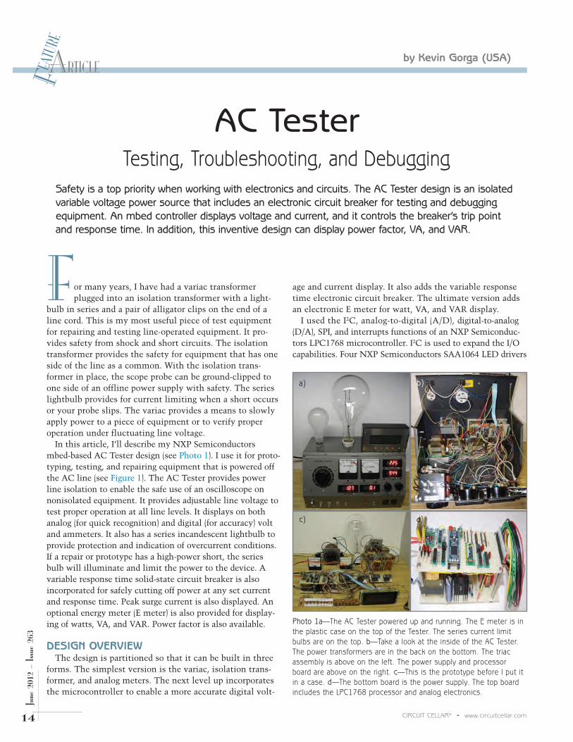
In this article, I’ll describe my NXP Semiconductorsmbed-based AC Tester design (see Photo 1). I use it for proto-typing, testing, and repairing equipment that is powered offthe AC line (see Figure 1). The AC Tester provides powerline isolation to enable the safe use of an oscilloscope onnonisolated equipment. It provides adjustable line voltage totest proper operation at all line levels. It displays on bothanalog (for quick recognition) and digital (for accuracy) voltand ammeters. It also has a series incandescent lightbulb toprovide protection and indication of overcurrent conditions.If a repair or prototype has a high-power short, the seriesbulb will illuminate and limit the power to the device. Avariable response time solid-state circuit breaker is alsoincorporated for safely cutting off power at any set currentand response time. Peak surge current is also displayed. Anoptional energy meter (E meter) is also provided for display-ing of watts, VA, and VAR. Power factor is also available.
DESIGN OVERVIEWThe design is partitioned so that it can be built in three
forms. The simplest version is the variac, isolation trans-former, and analog meters. The next level up incorporatesthe microcontroller to enable a more accurate digital volt-
14 CIRCUIT CELLAR® • www.circuitcellar.com
June
201
2 –
Issue
263
Safety is a top priority when working with electronics and circuits. The AC Tester design is an isolatedvariable voltage power source that includes an electronic circuit breaker for testing and debuggingequipment. An mbed controller displays voltage and current, and it controls the breaker’s trip pointand response time. In addition, this inventive design can display power factor, VA, and VAR.
F
FEAT
URE
ARTICLEby Kevin Gorga (USA)
age and current display. It also adds the variable responsetime electronic circuit breaker. The ultimate version addsan electronic E meter for watt, VA, and VAR display.
I used the I2C, analog-to-digital (A/D), digital-to-analog(D/A), SPI, and interrupts functions of an NXP Semiconduc-tors LPC1768 microcontroller. I2C is used to expand the I/Ocapabilities. Four NXP Semiconductors SAA1064 LED drivers
a) b)
c) d)
Photo 1a—The AC Tester powered up and running. The E meter is inthe plastic case on the top of the Tester. The series current limitbulbs are on the top. b—Take a look at the inside of the AC Tester.The power transformers are in the back on the bottom. The triacassembly is above on the left. The power supply and processorboard are above on the right. c—This is the prototype before I put itin a case. d—The bottom board is the power supply. The top boardincludes the LPC1768 processor and analog electronics.
Testing, Troubleshooting, and Debugging

www.circuitcellar.com • CIRCUIT CELLAR® 115
June
201
2 –
Issue
263
are used to display cur-rent, voltage, trip cur-rent, and response time.A Texas InstrumentsPCA9539 I2C – I2C I/Oexpander is used to pro-vide switch inputs, portoutputs, and key pressinterrupts. AnotherPCA9539 provides adot-matrix LCD inter-face for the E meter. AnNXP SemiconductorsPCA9507 two-wire serialbus extender bridges the3.3-V and 5-V I2C buses.Five analog-to-digitalconverter (ADC) chan-nels are used to measure AC current,line voltage, load voltage, trip currentsetting, and response time setting. Thedigital-to-analog converter (DAC) isused to set the latest high-current peakvalue for the overcurrent comparator.The SPI bus is used to communicatewith an Analog Devices ADE7753energy metering IC.
The mbed board enabled rapiddevelopment. It provided a pin-in-hole adapter for the LPC1768 foreasy hardware prototyping. It also
provided a function for nearly everyI/O requirement. This cut down thetime to get the LPC1768 up and run-ning, as well as the time required towrite the final program.
AC POWER INPUTThe basic function of the AC Tester
is to provide a variable, isolated, andprotected source of line voltage fortesting, debugging, or repairing equip-ment. Figure 2 shows the powerinput section. This would be the
most basic form of theAC Tester without anyof the added featuresprovided by the micro-controller. The linevoltage comes inthrough a switch cir-cuit breaker. It feedsthe variac for voltageadjustment. The LEDpower indicator D1uses the capacitivereactance of C1 insteadof a resistor that wouldproduce heat andrequire a high wattage.The variac bypassswitch enables the
variac to be bypassed for supplyingnominal line voltage. This alsoenables the variac to be lower cur-rent, if desired. In that way, you canuse it for low-current testing andbypass it for high-current work. Thiswould enable you to use a less expen-sive lower-current variac. A Normal/Boost switch enables the line voltageto be raised above the nominal level.The line voltage then flows throughan isolation transformer.
I used a pair of UPS power transform-ers to keep costs down. UPSeswith bad batteries are inexpensiveand commonly found. I used thetransformers from four identical600-VA units. They are wired backto back to provide 1:1 isolation.They can be switched to parallelfor higher current or series forhigher voltage (220-V) operation.Microwave oven transformers arealso a possibility for the isolationtransformers. You would have toremove the high-voltage secondaryand magnetic shunt, and thenwind a suitable VA secondary. Thetradeoff would be the number ofturns for a higher voltage thatwould enable a smaller wire forlower current. The line voltagethen passes through M1, an analogAC ammeter.
Analog and digital meters bothhave their places. The analogmeters provide for quick observa-tion and indication of fast dips oroscillations. They can provide asignificant amount of information
Figure 1—Input power is run through a variac and an isolation transformer. Itthen flows through current-limiting lightbulbs, an electronic circuit breaker, andan optional energy meter. The mbed processor measures the voltages and cur-rents for the digital displays. It also controls the electronic circuit breaker.
2
mbed
Variac Isolationtransformer
Electronic circuit breaker
Energymeter
LCD
Voltagedisplay
Response-timedisplay
Trip–currentdisplay
Currentdisplay
Figure 2—The AC Tester power input section includes the variac, isolation transformer, current-limiting lightbulbs, and meters. This is the most basic form of the AC Tester without any frills.

and do so while using as little current as possible, can dra-matically extend useful lifetimes.
Renesas’s RL78 MCUs are recommended solutions forembedded systems that mandate low-power operationrequirements because they provide advanced power-man-agement capabilities.
These functions enable the MCU to run with exceptionalpower efficiency in the normal Run mode; disable CPUoperation, saving power in Halt mode (enabling fast CPUwake-up time); disable more of the MCU functions in theStop mode to save the most power (at the expense of alonger CPU wake-up time); and deliver even greater powersavings with Snooze mode. Figure 1 depicts an operationalflow diagram for these three modes.
SNOOZE MODE OPERATIONThe Snooze mode enables some peripheral functions to
wake up and execute simple operations while the rest ofthe MCU is stopped. This saves a significant amount ofpower compared to the Run or Halt modes because inSnooze mode, the CPU is off and only the peripherals thatmust operate are enabled.
Data reception from the synchronous serial port, theUART, or a data conversion by the analog-to-digital con-verter (ADC) can operate in the Snooze mode by waking upthe associated port, but not the CPU.
The ADC can “wake up” when the real-time clock(RTC) or the interval timer generates interrupt signals tostart a conversion. Similarly, the synchronous serial portcan “wake up” when the serial clock input pin edge isdetected, and the UART can “wake up” when an edge on
Renesas RL78
I
ADVERTISEMENT by Mohammed Dogar
n our green energy world, many electronic designs aredriven by requirements for reduced size, improved
scalability, intelligent functionality, and most importantly,low power consumption.
The Renesas RL78 microcontroller (MCU) family isspecifically designed to meet these demands by incorporat-ing the highest peripheral integration, intelligent CPUarchitecture, and advanced power-management capabilitiesto enable “true low-power design.”
In addition to excellent general low-power characteris-tics, RL78 MCUs incorporate special functions to mini-mize operating current. Major sections of the MCUs can beturned off, while key peripheral blocks of the device con-tinue to function.
This smart low-power operation is achieved with theunique Snooze mode capability. Snooze mode dramaticallyreduces the power consumption of many typical MCUfunctions. The power savings are accomplished by allowingcommon data acquisition or data-transmission functions tooperate without the need to wake up the CPU. This opera-tional flexibility is a significant advantage over other low-power modes in which the CPU must remain active andassist with common peripheral functions.
In a system that periodically measures an analog signal,the Snooze mode enables an RL78/G13 MCU to achievemore than 30% reduction in the system’s average powerdissipation compared to an implementation without thismode.
Besides Snooze mode, RL78 MCUs have other impor-tant low-power characteristics that are valuable forpower-constrained designs. Their wide operating range,from 1.6 to 5.5 V, suits battery-based applicationswhere the voltage (VCC) drops over time as the bat-tery gradually discharges.
REDUCED POWER CONSUMPTIONIn extreme applications, some battery-operated
equipment must run off a battery for its entire oper-ating lifetime, without any recharges whatsoever.Such designs require the lowest operating currentpossible. It is absolutely critical to turn off functionsin the system whenever they aren’t needed and wakeup functions only when they’re required. The abilityto wait in a very low-power state until action isrequired and then wake up to take necessary action, FFigure 1—An operational flow diagram of the MCU functions
Halt
CPU
CPU
CPU
CPU
Clock
Clock
Clock
Clock
Peripheral device
Peripheral device
Peripheral device
Peripheral device
Main run
Stop
Conditionmatch
No conditionmatch
Snooze
Snooze modereduces powerconsumptionby more than 30%
Standby
Running
The True Low-Power MCU Platform

Mohammed “Mo” Dogar works for Renesas Europe
as a product marketing manager, focused on pro-
moting and selling microcontroller devices to major
OEMs and distributors. Mo’s group defines and
develops MCU product roadmaps and development
support infrastructure for wide range of industrial and
consumer electronics applications.
To register and enter the RL78 Green Energy Challenge, go to: www.circuitcellar.com/renesasrl78challenge
the RXD input is detected.After any data reception operation in Snooze mode is
completed, a “match condition” is checked. If the condi-tion is a match, then the MCU exits the Snooze mode andenters the Run mode. If the condition isn’t a match, opera-tion returns to the Stop mode. Thus, the CPU can be acti-vated only when the data received requires action from theCPU. Figure 2 depicts Snooze mode using the ADC trig-gered by a timer.
For example, because A/D conversion uses only 0.5 mAin Snooze mode, rather than 5 mA in Run mode, dramatic
power consumption advantages are obtained. Thus, an A/Dconversion can be performed in Snooze mode using only0.5 mA, 90% less than the 5 mA required to make a con-version in Run mode.
NOW IT’S YOUR TURNI discussed the ultra-low-power features of the RL78
MCUs, now what can you do with them? How will youuse the energy-saving features of the RL78 in your projectfor the RL78 Green Energy Design Challenge? What’s more,how can you incorporate these features into your everydaydesign and push the green energy envelope to the nextlevel, working to shape the future?
Figure 2—Snooze mode using the ADC triggered by a timer
Analog input
Upper limit
Lower limit
ADC with trigger by timer
Time
ADC values out of range: wake upthe CPU and process the results
Circuit Cellar feature articles are contributed by professional engineers, academics, and students from
around the globe. Each month, the editorial staff reviews dozens of article proposals and submissions.
Only the best make it into the pages of this internationally respected magazine.
Get PUBLISHED. Get NOTICED. Get PAID.
Do you have what it takes?
Contact C. J. Abate, Editor-in-Chief,
today to discuss the embedded design projects
and programming applications
you’ve been working on and
your article could be featured
in an upcoming issue
of Circuit Cellar magazine.
ADVERTISEMENT

will be noticeable across all the pixels that change bright-ness and color values between the two frames. Many ofthem will be the body of the person standing in front of thecamera.
Of course, a few things can be done to improve the accu-racy of the detection and to compensate for changes in thescene lighting. Shadows are one thing that causes problemswith this approach.
Testing this idea was straightforward. With my laptop’swebcam and a few lines of code, I could capture animage, store it, and compare it with another frame usingProcessing, which is an open-source development envi-ronment based on Java that can be used to create media-rich applications. It was developed at MIT and is freelyavailable for Windows, Linux, and OS X. During the lasttwo years, Processing has been my preferred choice forprototyping.
here is no doubt that Microsoft’s Kinect motion-sensing device has been a huge commercial success.
What is a bit less known is the story of how people havebeen hacking the device for a variety of purposes.
For those of you who’ve been living in a cave for thepast few years, Kinect is a peripheral device forMicrosoft’s Xbox 360 game console (see Photo 1). It sens-es user motion for a hands-free gaming experience. Youmove your arms and legs in front of a TV set and yourbody gestures are translated to your character in thegame. It could be said that Kinect is a camera, but it ismuch more than that.
Circuit Cellar is not a gaming magazine, so you may bewondering what this article is all about. Let me start fromthe beginning.
ART PROJECTI recently worked with Rubén Tortosa—local
artist, Fine Arts professor, and friend—to obtain thesilhouettes of the visitors of a given installation forhis art exhibit titled “TRAS (la espera).” This sil-houette would later be printed on one of the exhib-it’s walls. Photo 2 shows the wall being printed.The initial idea was to use a computer vision algo-rithm called background subtraction. If you set acamera facing an empty wall, a frame with theempty wall scene can be captured and it later canbe subtracted from the next frames captured. If aperson is then in front of the camera on a newframe, the difference between these two frames
336 CIRCUIT CELLAR® • www.circuitcellar.com
June
201
2 –
Issue
263
You can accomplish a variety of computer vision-related tasks with a microcontroller, bipolarstepper motors, and a depth camera. This article details how to use embedded technologywith Microsoft’s Kinect motion-sensing device for innovative image-processing applications.
Image Processing SystemDevelopment
T
FEAT
URE
ARTICLEMiguel Sánchez (Spain)
Use an MCU to Unleash the Power of Depth Cameras
Photo 1—A structured light pattern comes from the Kinect’s leftmost “eye.”

the optical technology used by Kinect to Microsoft andother partners, released an open-source official drivercalled OpenNI.
THE DEVICEAs you can see in Photo 1, the Kinect has coin-size cir-
cles on its plastic frame. One is just a regular webcam.Behind the other two is where the magic happens. Kinectutilizes structured light using an infrared laser and aninfrared camera to capture the reflection of that light pat-tern. Processing of the latter image determines the depth ofeach pixel of the infrared image.
In the depth image, each pixel value represents thedistance from the Kinect to it. That means a 3-D repre-sentation of the scene is obtained, where each pixel hasan X,Y coordinate plus the depth value, which is the Zcoordinate.
The distances measured range from 30” to 18’. Anythingcloser or farther away is represented as zero distance.Kinect has a tilt motor to make user tracking easier. Youcan command it to raise or lower the device attitude so theuser remains completely inside the scene. It also has athree-axis accelerometer that detects any motion of thedevice. Audio commands are possible as the device also hasfour microphones. Finally, you can switch one front LEDon or off. It can flash in two colors in response to com-mands from your computer.
THE LIBFREENECT LIBRARYDue to the effort of volunteers for the OpenKinect Proj-
ect, a library and bindings for different programming lan-guages are available. As it is the result of hacking the USB
THE KINECT HACKWhile I was implementing the aforementioned approach,
an unexpected turn of events occurred. Kinect hackingstarted to get news coverage.
As I mentioned, Kinect was originally presented on thenews as a new gaming peripheral for a game console. Noth-ing in the marketing campaign suggested Kinect could beused for any other purpose. However, Kinect uses USB toconnect to the Xbox 360 game console.
Given the features that were apparent from the availablegames, many people started to think this little device couldhave many interesting uses beyond gaming. There was aproblem though: neither drivers nor documentation wereavailable. And then some people decided that it might bepossible to reverse-engineer the protocol Kinect uses overUSB. There are hardware-based USB sniffers that can logthe two-way communication between an Xbox 360 and aKinect device.
MIT-trained engineer and entrepreneur Limor Fried ofAdafruit Industries bought a Kinect and obtained a trace ofthe USB communication. But, instead of sitting there try-ing to figure out how it worked, she took the 2.0 approachand crowd-sourced the research. Her company offered a$3,000 bounty to the first person who figured out how thedialog worked based on the communication logs she pro-vided on the company website. The wait was not long. Afew hours later a Spanish student, Hector Martín, had awinning entry.
Initially, Microsoft didn’t react well to Kinect hacking.There were even rumors of lawsuits. But since then, thewaters have calmed and an SDK for Windows 7 is nowavailable. This means Microsoft no longer has a problemwith people using Kinect for purposes other than playingwith Xbox.
As a result of the hacking effort, an unofficial open-source driver became available and an interesting set ofdetails about the device and its capabilities became pub-lic. Weeks later, PrimeSense, the company that licensed
www.circuitcellar.com • CIRCUIT CELLAR® 337
June
201
2 –
Issue
263
Photo 3—This sample Processing program shows both types ofKinect images: RGB video and depth image. Notice how similar thisis to the Arduino integrated development environment.
Photo 2—The exhibit featuring the finished project created quite astir with the public. Here you can see a front view of the wall being“printed.”

work for a small company that focuses onembedded systems and software design.
When we started in the late 1980s, we had noreputation outside our previous industries. Inorder to get work, it was important for us toestablish our credibility and to demonstrate ourexpertise. Here’s how we did that during thoseearly years.
After we got through the first level of vet-ting with a new company (we weren’t crimi-nals and at least we talked a good story), ourclients would ask us for a proposal to eithermodify their existing code or to create newcode based on the functionality of their oldcode. After the exchange of a nondisclosureagreement, they would send us their sourcecode to enable us to quote the job. Duringthat process, I would immediately look attheir serial drivers because I know this is anarea that is usually prone to errors. Most serialdrivers are interrupt-driven and thus requireknowledge of how to design concurrentthreads in embedded systems. In our ownexperience and in the experience of others, wehad seen that there were many possible pit-falls. If we could help our clients solve anexisting problem quickly and for no charge, Ithought this would both establish our credi-bility and demonstrate our expertise. So Iwould briefly look in their code for some ofthe common flaws we had both created andseen throughout years of dealing with inter-rupt-driven serial drivers. In almost 50% ofthe cases, we were able to find a real problem
444 CIRCUIT CELLAR® • www.circuitcellar.com
June
201
2 –
Issue
263
I
by Bob Japenga (USA)
Concurrency in EmbeddedSystems (Part 1)
Most embedded systems have concurrency requirements that designers andprogrammers must identify, understand, and manage. This article is the first in aseries about the topic. Concurrency is defined and pitfalls are examined.
An Introduction to Concurrency and Common Pitfalls
EMBEDDED IN THIN SLICES
in their code—and it was always caused byconcurrency issues. Sometimes they wereserious and sometimes they were relativelyharmless.
Getting concurrency right is not easy. Overthe next several articles, I will address concur-rency as it relates to embedded systems. In thisarticle, I define concurrency, list some of thecommon pitfalls, and look at one of them inparticular. I will address other common pitfallsin upcoming articles.
DEFINING CONCURRENCYConcurrency takes place any time two or
more activities can happen in the same timesegment. For example, I can concurrently washthe dishes, watch TV, and listen for a text mes-sage on my phone. A phone can concurrentlynotify you of incoming calls while displaying aTV program.
According to Wikipedia, in computer science,
HELPFUL DEFINITIONSThread: Any functionality that can beactive during the same time segment. Itcan be in hardware or software.Blocked: When a software thread relin-quishes control of the processor to theoperating system.Preempt: When one thread interruptsanother.

with interrupts, or with hardware. In amultitasking OS, you would put ablocking delay at the end of the high-speed thread. In addition, you wouldenable the external thread to preemptthe UI loop. This means the externaldevice thread does not have to waituntil the UI thread is complete beforeit can start. This could be done by giv-ing the external device thread a higherpriority than the user input thread.For example, if you are polling theexternal input every 10 ms, you wouldbe “interrupting” the UI loop someplace in the code every 10 ms. Withinterrupts on the external device, youwould basically be doing the samething without the need for a threaddelay. You would be “event-driven”rather than periodically polling. Butyou would still be interrupting the UIthread every time the external devicechanged. Finally, you could solve thisby using or creating hardware thatcould obtain the external data whilethe UI software is busy and go back toyour single-thread solution. Table 2provides a look at solving it using themultithreaded OS. Notice that the UIthread never stops but polls continu-ously (sometimes this is called the idlethread). The external device threadblocks (gives other threads the oppor-tunity to run) and thus effectivelypolls the external input every 10 ms
www.circuitcellar.com • CIRCUIT CELLAR® 445
June
201
2 –
Issue
263
embedded system with one input, oneoutput, a very fast logging device, anda graphical user interface (GUI). Youcan create such a system with orwithout concurrency. You could, forexample, create software with a singleloop as shown in Table 1. We haveseen literally scores of systemsdesigned like this. They are simple.They work. No concurrency is neces-sary in the software. But wait aminute. There is concurrency in thissystem. The user and the externaldevice can change things at the sametime. That means the system has con-currency. But does the software needconcurrent threads to handle this?Well, that depends. If the inputchanges more quickly than our timeto execute our simple loop, we have aproblem. If it takes 100 ms to write toour graphics display and our externalinput device can do something every20 ms, we would miss critical datawhile going through the loop.
So how do we solve that? We couldstart sprinkling I/O reads into themiddle of the graphics library, but thatis extremely messy. We could createtwo concurrent threads in our system:one to process the user interface (UI)and one to process the external device.In an embedded system, this could beaccomplished in three ways: with amultitasking operating system (OS),
“concurrency is a property of systemsin which several computations areexecuting simultaneously, and poten-tially interacting with each other.”
Of course, if they don’t interact,there are no pitfalls, but they are stillconcurrent. However, they almostalways interact in some way and thatis what creates the problems.
COMMON CONCURRENCY PITFALLSAny embedded system that has con-
currency built into its design can expe-rience one or more of the followingproblems: Race Conditions—where theorder of execution affects the outcomeof a given result. Corrupting of SharedResources—where shared resources areused by two or more concurrentthreads. Logical Complexity CreatingLess than Airtight Algorithms—themore things that can affect each other,the more difficult it is to carefullythink your design through and make itbullet proof. Deadlock—where func-tions stop working for no apparentreason. Time-of-Check-to-Time-of-Use (TOCTTOU)—I read the datafrom an input and make a decision,but by the time I use the data, the datahas changed. Priority Inversion—wherea lower-power thread locks out a higher-priority thread.
I will cover these conditions overthe next several articles. In this arti-cle, I’ll address priority inversion:what it is and how to avoid it.
WHAT IS PRIORITY INVERSION?Given the number of problems
concurrency has given me over theyears, how have concurrency issuesranked in the history of major soft-ware failures? As I looked over vari-ous lists of “the worst softwarebugs,” I found that only a few ofthem directly involved these com-mon pitfalls. The Mars Pathfinderbug was one of them. Initially flaw-less in its fulfillment of a very com-plicated mission, early on, thePathfinder began experiencing peri-odic resets and the subsequent lossof data. The cause was a classic caseof priority inversion.
To illustrate concurrency and howpriority inversion can happen in anembedded system, I’ll create a simple
Table 1—Steps that single-loop software may take in a design without built-in concurrency
Table 2—Steps that a user input thread and an external device thread may take in a systemdesign with two threads
Our Example Design with Two ThreadsUser input thread External device threadCheck for user input Check to see if something changed in the external world
(input changed state or character received)
Process the user input Process the changes from the input from external world and set the output accordingly
Update the display Log the external data to our logging device when freeLog the user data to ourlogging device when free
Block for 10 ms
Rinse and repeat Rinse and repeat
Our Example Design Without ConcurrencyCheck to see if the user has hit a keyOutput the new display as a result of the key press (takes about 100 ms)Check to see if something changed in the external world Process the changes from the input from external world and set the output accordinglyLog the user input and the output state to our logging device (takes about 50 ms)Rinse and repeat

Frequency mixers are essential to radio frequency (RF) designs. They areresponsible for translating a signal up or down in frequency. This articlecovers the basics of RF mixers and their real-life applications.
Radio Frequency Mixers
by Robert Lacoste (France)
elcome back to the Darker Side. This month I’ll present a topic that
frightened me for years: mixers—more precisely,radio frequency (RF) mixers. As a kid, when Istarted playing with a soldering iron, buildingalarms or other gadgets, my father gave me hun-dreds of old radio magazines. They were full ofshort-wave receiver schematics, with strangenames like “intermediate frequency” (IF) and“super-heterodyne.” I tried to understand, butfor a long time I safely restrained myself to thedigital side. In fact, since using 7400 and 4011logic chips was comparatively easy, moving toslightly more complex systems built around6502 or Z80 chips was not so hard. I startedplaying with RF only 15 years later.Discovering how a mixer actuallyworks was a revelation!
WHAT IS A MIXER?RF usually means very high fre-
quencies. I know there are very lowfrequency (VLF) systems in serviceto communicate with submarines,but let’s stay generic. The carrierused to transmit the informationover the air has a frequency ordersof magnitude higher than the infor-mation stream itself. For example,FM is broadcast around 100 MHz,whereas the stereo audio channeluses only some tens of kilohertz ofbandwidth. Therefore, it is useful to
THE DARKER SIDE
translate a slice of the frequency spectrumfrom low frequencies to high frequencies for atransmitter, or from high frequencies to lowerones for a receiver. That’s where frequencymixers shine. A frequency mixer is a frequencytranslation device that could be used either tomove up (up convert) or down (down convert)any part of the spectrum.
Let’s start by considering frequency mixersas black boxes. A mixer has one signal inputport, one so-called local oscillator (LO) inputport, and one signal output port, as shown inFigure 1. For a down converter, the input is tra-ditionally named RF and the output is IF. Thisis the opposite for an up converter.
June
201
2 –
Issue
263
CIRCUIT CELLAR® • www.circuitcellar.com58
W
Figure 1—A mixer is a three-port device: a signal input, an LO input,and a signal output. When used with a frequency filter, it generateseither a sum or a difference frequency. It can then increase (up convert)or decrease (down convert) the frequency of an RF signal.
Down converter
FRF
FIF
FIFF
RFF
IFF
LO
FRF
FLO
FLO
FLO
= 340 MHz
= 300 MHz
Filter
Filter
Up converter
=
= = 340 MHz
– = 40 MHz
+
= 300 MHz
= 40 MHz

last term will inevitably include theproduct V1 × V2 of the two input volt-ages. So any nonlinear device could beused as a mixer, but of course, someare more effective or “cleaner” thanothers!
MIXER INTERNALSWhat is the simplest nonlinear
electronic device? It is a diode, as thecurrent going through it is not pro-portional to the voltage applied on itsterminals. That brings us to the oldso-called unbalanced diode mixer. Itsschematic, as well as a simulation Imade using Labcenter Electronics’sProteus CAD tool suite, is shown inFigure 3. To better understand thisschematic, you must know that careis usually taken to set the LO signalpower at a far higher power than themixer input signal. The LO mainlydefines the diode behavior. When theLO signal is positive enough, thediode is conducting. When the LOvoltage is negative, the diode is in ablocking state. As the small inputsignal is added to the LO voltage, itis chopped by these alternating LOcycles: the input signal passesthrough when the LO is in its posi-tive half period.
So, this means theinput signal is multi-plied by a square signalat the LO frequency.There is a kind of volt-age multiplier, and thismakes a mixer. How-ever, as a square signalis more complex thana sine, it includes afundamental but alsoharmonics. Therefore,such a diode-basedmixer generates therequired difference andsum frequencies asdescribed, but alsoplenty of harmonics ofboth LO and RF signalsas well as more com-plex combinations. Infact, you will find inthe output any fre-quency that could begenerated as (n × FLO +m × FRF), where n and
www.circuitcellar.com • CIRCUIT CELLAR® 559
June
201
2 –
Issue
263
NONLINEARITY HELPSA trigonometrical identity is funda-
mentally the basis of all frequencymixers. Take a deep breath and repeatafter me: 2.cos(a).cos(b) = cos (a+b) +cos (a-b).
I’m sure you learned this one, no?If you prefer a graphical version, seeFigure 2, which shows a 300-MHzsine wave multiplied by a 340-MHzsine wave. The result is a slow 40-MHzsine with an added high-frequency,640-MHz sine. That’s it. Basically mul-tiplying two sine waves generates asignal that is the sum of two sines,respectively, at sum and difference fre-quencies. Great. That’s exactly whatwe were looking for!
Therefore, you can build a frequencymixer with any electronic part that“multiplies” two input voltages, andthey are numerous. More precisely, itwill work as long as you use any non-linear component. Why? Imagine thatyou have two input voltages, V1 andV2. Add them and send them through anonlinear device. Their output will bea nonlinear function of x = V1 + V2, sayf (V1 + V2). But you can almost alwaysapproximate this function by a secondorder equation f(x) = a + bx + cx2. Ifyou do the math, you will see that the
What is the behavior of an ideal fre-quency mixer? Given an input fre-quency FIN and an LO frequency FLO, itgenerates a sum of two signals on itsoutput, with respective frequencies ofthe sum FIN + FLO and the differenceFIN – FLO (or the opposite, whichever ispositive) of the original frequencies.You can then filter the output signalto recover the component you arelooking for. For example, a low-passfilter with select FIN – FLO.
You must know that a mixer isfundamentally a linear device, aslong as it is used correctly. Its outputwill be doubled in amplitude if youdouble the amplitude of the inputsignal, and the phase relationshipbetween input and output is main-tained. Moreover, mixers—at leastpassive ones, as you will see—arereversible devices. With the samemixer you can input a signal on itsIF port and use the RF port as an out-put, or the opposite.
You must understand that a mixeris one of the key building blocks ofnearly all RF systems, used as a fre-quency translator or as a modulator(with the IF signal modulating the LOone). If you want to know how theywork, just keep reading.
Figure 2—When two sine signals are multiplied, the result is the sum of two sines of sum and differencefrequencies. This is the basic mechanism used by a frequency mixer. The OpenOffice spreadsheet used togenerate this figure is available on Circuit Cellar's FTP site if you want to play with it.
FRF
FLO
FRF
FLO
- FRF
FLO
+
cos
cos
a
RF
( ) × ( ) ( ) −( )⎡⎣ ⎤⎦
×
cos b = 12
cos A + B + cos a b
tΩ(( ) × ×( ) ( ) ×{ } − cos t = 12
cos + t + cos LO RF LO RF LΩ Ω Ω Ω Ω OO t( ){ } ×⎡⎣ ⎤⎦
