j.r.krenn – nanotechnology – cern 2003 – part 1 page 1 nanotechnology j.r.krenn institute for...
TRANSCRIPT

J.R.Krenn – Nanotechnology – CERN 2003 – Part 1 page 1
Nanotechnology
J.R.KrennInstitute for Experimental Physics
Karl-Franzens-University Graz, [email protected]
nanooptics.uni-graz.at

J.R.Krenn – Nanotechnology – CERN 2003 – Part 1 page 2
Literature[1] K.E.Drexler, Nanosystems, Wiley, New York, 1992
[2] H.-G.Rubahn, Nanophysik und Nanotechnologie, Teubner, Stuttgart 2002 (german)
[3] R.Waser (ed.), Nanoelectronics and Information Technology, Wiley-VCH, Weinheim, 2003
[3] M.Köhler, Nanotechnologie, Wiley-VCH, Weinheim, 2001 (german)
[4] V.Balzani et al., Molecular Devices and Machines, Wiley-VCH, Weinheim, 2003
[5] I.Fujimasa, Micromachines, Oxford Univ. Press, Oxford, 1996
[6] Nanotech, Special Issue Scientific American, September 2001
• www.nanotechweb.org (news service)• www.nano-tek.org (general)• www.foresight.org/NanoRev/index.html (general)• www.sunsite.nus.edu.sg/MEMEX/nanolink.html (link list)
Illustrations were taken from websites, books and journals. Great care was taken to assign the respective copyrights.
The names of companies or products mentioned in the following may be the trademark of their respective
owners.

J.R.Krenn – Nanotechnology – CERN 2003 – Part 1 page 3
What is Nanotechnology? (1)
– 1931 M.Knoll, E.Ruska: Electron Microscope– 1959 Feynman's Talk
'There's plenty of room at the bottom'www.zyvex.com/nanotech/feynman.html
– 1974 N.Taniguchi: 'Nanotechnology'– late 80's K.E.Drexler
atom-by-atom 'assembler'
– 90's Molecule-by-Molecule supramolecular chemistry
– late 90's Submicron Scaled Matter
www.foresight.org

J.R.Krenn – Nanotechnology – CERN 2003 – Part 1 page 4
What is Nanotechnology? (2)
www.foresight.org Science november 9, 2001Scientific American september 2001
Problems: (i) energy supply, communication, ...
(ii) scalability, molecular fluctuations, noise, 'sticky' and 'fat' fingers
J.R.Krenn – Nanotechnology – CERN 2003 – Part 1 page 5
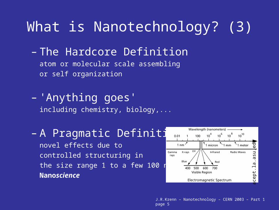
What is Nanotechnology? (3)
– The Hardcore Definitionatom or molecular scale assembling
or self organization
– 'Anything goes'including chemistry, biology,...
– A Pragmatic Definitionnovel effects due to
controlled structuring in
the size range 1 to a few 100 nm
Nanoscience ace
pt.
la.a
su.e
du

J.R.Krenn – Nanotechnology – CERN 2003 – Part 1 page 6
Why Nanotechnology?
To optimize properties readily exploitedincreasing speed
mechanics: lower response time, higher resonance frequencyelectronics: shorter signal paths, lower parasitic RCL, lower power dissipationoptics: faster (and higher density) storage, modulation, switching, routing
material demand (e.g., Ge)
To exploit novel propertiesapproaching typical wavelength scales, increasing surface / volume ratiomaterials: decreasing crystallite size (mechanical strength, magnetic
storage), nanoparticles for catalysis or opticselectronics: quantum effectsoptics: near-fields, quantum communication

J.R.Krenn – Nanotechnology – CERN 2003 – Part 1 page 7
Outline (1)
• Methods
• Electronics
• Optics
• Mechanics & Materials

J.R.Krenn – Nanotechnology – CERN 2003 – Part 1 page 8
Outline (2)
1. Methods• Microscopy and
(Top-Down) Lithography• Nanoimprinting• Bottom-Up Structuring
2. Electronics• The Semiconductor Roadmap• Energy Quantization and
Quantum Dots• Conductance Quantization• Molecular Electronics• Scanning Tunneling Microscopy
3. Optics• Micro-Optics• Near-Field Optics• Scanning Near-Field Optical
Microscopy• Surface Plasmons
4. Mechanics & Materials• Micromechanics• Atomic Force Microscopy• Nanophase Materials• Carbon Geometries

J.R.Krenn – Nanotechnology – CERN 2003 – Part 1 page 9
NANOTECHNOLOGYPart 1. Methods in Nanotechnology
• Microscopy and (Top-Down) Lithography– Optical– Electron– Scanning Probe
• Nanoimprinting
• Bottom – Up Structuring

J.R.Krenn – Nanotechnology – CERN 2003 – Part 1 page 10
Optical Microscopy
θλsin
61.0 0
nx =Δ
© Nikon
2
1 )(2)( √
↵
=
νν
νJ
I
resolution limit
Solid immersion lens (SIL)
transfer function
Micro-photoluminescence (a) with and (b) without SIL (www.uni-karlsruhe.de)
Immersion lens
αλπν sin
2r=
from [2]

J.R.Krenn – Nanotechnology – CERN 2003 – Part 1 page 11
Confocal Optical Microscopy
© Nikon
Marvin Minski 1955
Principle: confocal aperture rejects light not
originating from the focal plane; focussed light
beam & scanning (either light beam or sample)
High aperture focussing: (a)-(c) plots and
(d)-(f) log. plots of the intensity distribution
in the focal plane of a lens N.A.=0.966.
Intensity ratios of Ix:Iy:Iz=1:0.0081:0.192
M.M
ansu
ripur
, Cla
ssic
al O
ptic
s, C
ambr
idge
Uni
v. P
ress
, 200
2

J.R.Krenn – Nanotechnology – CERN 2003 – Part 1 page 12
Optical Lithography
dot.che.gatech.edu
Mask: Cr on glass; production by either focussed laser beam writing or electron beam lithography;phase shift masks
Light sources: Hg arc lamp (λ0=436, 365, 248 nm)
KrF laser (λ0=248 nm), ArF laser (λ0=193 nm),
F2 laser (λ0=157 nm)
Lens system: projection reduction typically 1:4
Structure transfer to photosensitive polymer resists

J.R.Krenn – Nanotechnology – CERN 2003 – Part 1 page 13
Electron Microscopy
)(2,
2 p
medvacEeUm
h
meU
h
−== λλ
mvpeUmvEk ===r
,21 2
λω hkpE === hh ,
eU
En p
med
vac −== 1λλ
U/V v/c λ/nm 10-1 6.3 10-4 3.91 2.0 10-3 1.2101 6.3 10-3 3.9 10-1
102 2.0 10-2 1.2 10-1
104 0.19 1.2 10-2
106 0.94 8.7 10-4
De Broglie wavelength of the electron

J.R.Krenn – Nanotechnology – CERN 2003 – Part 1 page 14
Transmission Electron Microscopy
buried hexagonal phase in cubic CdTe (www.nrel.gov)
www.biologie.uni-hamburg.de
Grain boundary in precipitatealuminum particle (www.lbl.gov)
electron-sample interaction
J.R.Krenn – Nanotechnology – CERN 2003 – Part 1 page 15
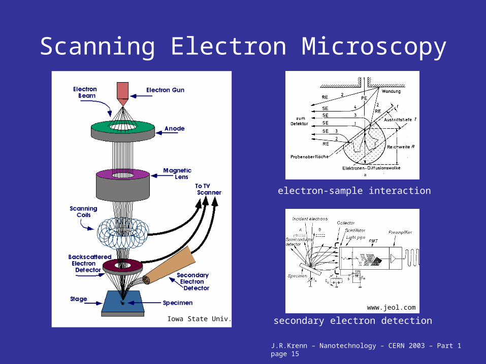
Scanning Electron Microscopy
Iowa State Univ. secondary electron detection
www.jeol.com
electron-sample interaction

J.R.Krenn – Nanotechnology – CERN 2003 – Part 1 page 16
Electron Beam Lithography

J.R.Krenn – Nanotechnology – CERN 2003 – Part 1 page 17
What else a photon or electron can tell
LEED Low energy electron diffraction
AES Auger electron spectroscopy
EELS Electron energy loss spectroscopy
UPS Ultraviolet photoemission spectroscopy
XPS X-ray photoemission spectroscopy
XRD X-ray diffraction
IPES Inverse photoemission spectroscopy
TDS Thermal desorption spectroscopy
STM Scanning tunneling microscopy
STS Scanning tunneling spectroscopy
.....
The Surface Science ToolboxOptical Spectroscopy
Abs., Trans., Refl.
Fluorescence, Raman
Harmonic Generation
Wave mixing etc.
Femtosecond time resolution

J.R.Krenn – Nanotechnology – CERN 2003 – Part 1 page 18
Scanning Probe Microscopy (1)
www.fysik.dtu.dk
constant gap mode constant height mode
www.ilp.physik.uni-essen.de

J.R.Krenn – Nanotechnology – CERN 2003 – Part 1 page 19
Scanning Probe Microscopy (2)
www.surfchem.kth.se, www.veeco.com
www.omicron.com
Tip: depending on probe type
Scanner: PZT piezoelectrics, electrostrictive
Mechanics: compact design
Electronics: preamplifier, PI feedback loop
Computer: scan control, data analysis
Vibration isolation
SPM lithography

J.R.Krenn – Nanotechnology – CERN 2003 – Part 1 page 20
Nanoimprinting
Nanoimprinting scheme
(following CD/DVD process)
T.Hoffmann, Univ. Wuppertal
Example: gold structures on silicon
PMMA resistS.Chou et al., J.Vac.Sci.Technol.B 14, 4129 (1996)

J.R.Krenn – Nanotechnology – CERN 2003 – Part 1 page 21
Soft Lithography
Michel et. Al., IBM J. Res. & Dev., Vol. 45, 2001Univ. of Delaware
Replicate Forming, Micro-Contact Printing, (Capillary Moulding)

J.R.Krenn – Nanotechnology – CERN 2003 – Part 1 page 22
Bottom – Up: Molecular Architecture
www.ifm.liu.se
Self assembled monolayers
R.D.Piner et al., Science 283, 661 (1999)
Epitaxial growth (MBE)
VOx on Pd (111) 7.8 x 7.8 nm2honeycomb (2 x 2)(surface-science.uni-graz.at)
AIN on SiC(0001)(www.asu.edu)

J.R.Krenn – Nanotechnology – CERN 2003 – Part 1 page 23
• Top – Down– optical (semiconductor industry)– electron (master production, research)– scanning probe (mainly research)
– Nanoimprinting !
• Bottom – Up supramolecular level
Summary: Lithography