journal of materials chemistry c - huji.ac.ilchem.ch.huji.ac.il/etgar/conductive...
TRANSCRIPT

11548 | J. Mater. Chem. C, 2016, 4, 11548--11556 This journal is©The Royal Society of Chemistry 2016
Cite this: J.Mater. Chem. C, 2016,
4, 11548
Conductive molecularly doped gold films
Hadas Naor, Yiftach Divon, Lior Iagher, Lioz Etgar* and David Avnir*
We describe a general synthesis of conductive gold thin films doped with entrapped organic molecules,
and demonstrate, for the first time, the immobilization of a redox couple within an electrode in a single
step. The resulting film is of dual properties: conductivity arising from the gold, and redox behavior
originating from the entrapped molecule. Faster electron-transfer rates are found for the entrapped
case, compared to adsorption. The conductivity of the film affects the organic molecule–metal interactions,
as seen in resistivity measurements, in Raman spectroscopy of the metal-entrapped molecules and from
a remarkable red shift of 30 nm in emission spectroscopy. Doping is found to affect the work function
of gold. Thin conductive doped metal films are of relevance to a variety of applications such as
electrochemical detectors, electrode materials for electrochemical impedance spectroscopy, micro and
nano electronics interconnects for packaging and for printed circuit boards. The ability to fine-tune the
work function opens the possibility to design the desired energy level gaps for optoelectronic applications
such as light emitting diodes (LEDs), solar cells and transistors.
Introduction
The development of the new family of molecularly doped metals,1
molecule@metal, opened the way to prepare many new func-tional materials, ranging from new catalysts,2,3 to biomaterials,4,5
to chiral metals,6,7 and more.8,9 Most applications are related topowders, discs and supported nanoparticles,10 but as many moreapplications are associated with thin films, we recently began thedevelopment of methodologies for the formation of thin filmsof doped metals.11,12 This was achieved by focusing on newelectroless-based methods which resulted in molecule@Ag12
and molecule@Au films.11 The original film morphologyobtained for the doped gold films11 was of disconnected islands,that is, the gold films were non-conductive. Since one of the keyfeatures of gold films, which leads to many of their applications,is conductivity, it was clear that this problem must be solved, ifapplications of these hybrid films are to be developed. Here, wereport the successful solution to that problem, and this enables,for instance, the first one-process preparation of a redox-activedoped gold film electrode. The transition from non-conductiveto conductive doped gold films is of relevance to variousapplications, including electrochemical detectors for micro-fabricated electrophoresis chips,13 electrode materials for electro-chemical impedance spectroscopy (EIS),5,14 micro and nanoelectronics interconnects for packaging and for printed circuitboards (PCBs),15,16 and electroconductive textiles.13,15 We recall
that the entrapment within gold described here is a 3D processin which the molecules are surrounded all around by the metalcrystallites, held with dipole, pi–pi, van der Waals and simplephysical caging interactions, while adsorption is a 2D processwhere the molecules are arranged on the surface in an orienta-tion which is dictated by a specific moiety of the adsorbed orchemisorbed molecule. 3D entrapment leads therefore to theability to connect almost any organic molecule to gold, withoutconsidering the specific properties of the molecule such ascharge or special functional groups. Indeed, in this work threedifferent molecules (Fig. 1) were entrapped within the conductivegold films: the cationic thionin (Th), the anionic bromocresolgreen (BcG), and the fluorescent rhodamine B (RhB), all resultingin molecule@Au composite films. These three dopants were alsoselected due to their ability to be used as markers in the differentcharacterization methods described below. We found that asa result of the induced conductivity, the interactions of the
Fig. 1 Molecules entrapped in gold conductive thin films using the metal-doping electroless processes.
Institute of Chemistry and the Center for Nanoscience and Nanotechnology,
the Hebrew University of Jerusalem, Jerusalem 91904, Israel.
E-mail: [email protected], [email protected]
Received 23rd August 2016,Accepted 12th November 2016
DOI: 10.1039/c6tc03648a
www.rsc.org/MaterialsC
Journal ofMaterials Chemistry C
PAPER
This journal is©The Royal Society of Chemistry 2016 J. Mater. Chem. C, 2016, 4, 11548--11556 | 11549
entrapped molecules with the gold have changed comparedto the non-conductive case. These changes were detected byRaman spectra from within the films, and by a large red shift inthe emission spectrum of RhB.
Experimental detailsChemicals and materials
Thionin acetate (Th), bromocresol green (BcG), rhodamine B(RhB), trisodium citrate tribasic dehydrate (99%), hydroxylaminehydrochloride (98%), poly(diallyldimethylammonium chloride)(PDDA) and gold(III) chloride (99.99%) were purchased fromSigma-Aldrich. The gold chloride was dissolved in a 1 M HClsolution. Glass slides (surface roughness o1 nm rms) werepurchased from Schott.
Formation of the doped conductive thin films
The conversion from the disconnected island morphology tothe conductive morphology required modification of previousprocedures10,17 as follows. First, colloidal gold was preparedfrom HAuCl4:19 12.5 mL of HAuCl4 1 M was dissolved in 50 mLtriple distilled water (TDW) and heated to boil under stirring;the solution was kept under these conditions until the endof the synthesis. 13 mg sodium citrate was dissolved in 1.25 mLTDW and the solution was added to the boiling gold saltsolution. After about a minute a grayish-blue hue appeared,gradually changing into a deep red wine color and the colloidwas stored at 4 1C after an additional 5 minutes of boiling.For deposition of the gold particles the glass slides were firstcleaned via 5 minutes of sonication with ethanol and dried witha nitrogen stream, followed by an ultraviolet ozone cleaningsystem (UVOCS) for 20 minutes (which can be replaced bycleaning with a piranha solution). The cleaned slides wereimmersed in 0.01 M PDDA solution for 2 hours, rinsed againwith water and dried under a nitrogen stream. The polymer-coatedslides were subsequently incubated overnight in the colloidal goldsolutions and the AuNP self-assembled on it. The gold layer wasrinsed with water and then dried under a nitrogen stream.The improvement of the adhesion and the uniformity of thecatalytic layer were achieved by dipping the AuNP-coated slidein an electroless solution containing 3.8 mL of 1.0 M HAuCl4
and 10.0 mL of 0.40 mM hydroxylamine hydrochloride for15 minutes under agitation. The slide was then taken out fromthe solution and immediately used for the metal dopingprocess: the slide was dipped again in a fresh electrolesssolution (3.8 mL of 1.0 M HAuCl4 and 10.0 mL of 0.40 mMhydroxylamine hydrochloride) to which 12.5 mL of 5.0 mMsolution of the dopant (each of the three dyes) was added andthe slides were then agitated for 60 minutes in that combinedsolution. It should be noted that this agitation step, along withthe formation of the gold-particle catalytic layer, are crucial forobtaining good conductive films; lack of these features resultsin island morphology. The final doped gold film was thenrinsed with water and dried under a nitrogen stream. The filmthickness was determined by using the non-erasable pen method.
Comparative surface deposition
Pure gold films were prepared as described above but withoutthe dopant. One drop of the dopant solution (at concentrationsof 25 mm (BcG), 5 mM (Th) or 2.65 mM (RhB)) was cast on thegold film and dried.
Cyclic voltammetry measurements
Cyclic voltammograms of free Th molecules in solution and ofTh@Au films were carried out using a CHI-630B potentiostat(CH Instruments Inc., TX, U.S.A.) in a conventional three-electrode cell comprising of a composite of the Th@Au filmas the working electrode, a platinum wire as the counterelectrode, and Ag|AgBr as the reference electrode. Voltammetrywas performed at different sweep rates (20, 40, 60, 80, 100 mV s�1)in acetonitrile containing 0.1 M tetrabutylammoniumtetrafluoro-borate (TBATFB) as the supporting electrolyte without Th in thesolution. A comparative three-electrode cell was carried out with aself-made gold film as the working electrode, prepared similarlybut without the Th, and 75 mM free Th in the solution.
Characterization and instrumentation
High resolution scanning electron microscopy (HR-SEM) obser-vations were performed using Sirion (FEI) and Magellan (400 L)microscopes, operating at 5 or 10 kV. Samples were preparedby placing a small piece of glass with a sample on it on a stubwith carbon tape. Raman and SERS (surface-enhanced Ramanspectroscopy) measurements were taken using a RenishawInVia Raman microscope with a maximum output of 300 mWat a wavelength of 785 nm for excitation (only 0.0001% powerof the laser was used). The Raman microscope includes anobjective Leica microscope. The grating for the 785 nm laser is1200 lines per mm. The electrical resistivity of Au films wasmeasured using an in-line Four Point Probe (Lucas Labs S-302-4).X-ray photoelectron spectroscopy (XPS) measurements were per-formed on a Kratos Axis Ultra X-ray photoelectron spectrometer.XRD measurements were carried out using a Philips automatedpowder diffractometer (with a PW1830 generator, PW1710control unit, PW1820 vertical goniometer, 40 kV, 30 mA, CuKa1 (1.5406 Å)). The crystallite size was calculated from theexperimental XRD data through the Scherrer equation usingthe TOPAS v.3 software, including all the observable peaks byaveraging the results from all the crystallites in the material.UV-vis absorption spectroscopy was carried out using a JascoV-630 spectrophotometer. Surface photovoltage spectroscopy(SPS) was performed on a KP technology system modelSKP5050-SPS040. Contact potential difference (CPD) betweenthe sample and the vibrating tip was measured using the Kelvinprobe technique. Samples were measured in a Faraday cageunder an air environment. Before the measurement, the sam-ples were stabilized with a tip for about 30 min. The workfunction (WF) was calculated according to WFsample = WFtip �CPD(tip�sample). Photoluminescence measurements were per-formed using an Edinburgh Instruments FLS920 FluorescenceSpectrometer. Samples were excited with monochromatizedlight from a Xe lamp. The emission was collected at a right
Paper Journal of Materials Chemistry C
11550 | J. Mater. Chem. C, 2016, 4, 11548--11556 This journal is©The Royal Society of Chemistry 2016
angle, dispersed using a double-monochromator and collectedusing a Hamamatsu R2658P-PMT.
Results and discussionFilm formation and characterization
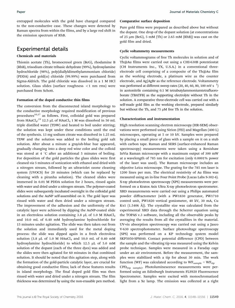
SEM and XRD. Typical SEM pictures (Fig. 2) show the compactdense granular morphology for all the doped films – Th@Au,BcG@Au and RhB@Au – in fact, even more compact than thepure gold film, prepared under similar conditions (Fig. 2d).Morphological effects of the type of dopant are seen as well: forinstance, RhB (Fig. 2c) induces irregular condensed shapes,less ordered and larger than in Th@Au (Fig. 2a), probably dueto the strong interaction between the sulfur group of Th and theforming gold crystal. To gain insight into the building blocksthat form the condensed aggregates, X-ray diffraction (XRD)pattern measurements were performed (Fig. 3). Comparison ofthe three composite molecule@Au with the pure gold filmshows that the typical XRD pattern of gold20 is retained in allcases: 2y = 38.21, 44.41, 64.61, 77.61 and 81.71, respectively, forAu(111), Au(220), Au(200), Au(311) and Au(222). Notably,although the 2y value did not vary compared to the fcc bulkgold,21,22 the crystallographic orientation of the Au(111) crystallo-graphic planes was the preferred growing orientation for thiselectroless process. The XRD measurements were also used tocalculate the average sizes of the elementary building blocks byusing Scherrer’s equation. These were found to be 16 nm,25 nm, and 34 nm for the composites Th@Au, BcG@Au, andRhB@Au, respectively, compared with 30 nm for the pure goldfilm. Interestingly, the larger particle size of RhB@Au also
translates to the larger aggregates and to the larger condensedislands of RhB@Au compared to the other films. The fact thatTh@Au has the smallest particles is apparently due to thechemical structure of Th (Fig. 1) – it is the only dopant whichhas sulfur in its structure, an element known for its stronginteraction with gold; these interactions slow the growth of theAu particle in this process.
Profilometry and film thickness. The film thicknesses weremeasured using profilometry (Fig. 4), which also providesinformation about the roughness. The average thicknessesare 120 nm, 176 nm and 166 nm for Th@Au, BcG@Au andRhB@Au, respectively, compared to 293 nm for the pure goldfilm. We propose that the fact that Th@Au is the thinnest,while pure gold is the thickest, is related to the observation thatTh@Au is composed of the smallest elementary buildingblocks, and the thicker films are composed of larger particles,in the following way: the proposed formation mechanismis – see ref. 1 and 10 – that Au seeds form first, the numberof which mainly depends on the concentrations of the gold ionsand the reducing agent, which is similar for all the samples,and then physisorption of the dopant molecules on these seedsstarts the entrapment process and dictates also the size of theforming crystallites. Thus, assuming similarity in the number ofinitial Au seeds and therefore also in the number of depositedparticles for all cases, means that smaller particles will form thinnerlayers: comparing the deposition processes for the same depositiontime (60 minutes) results in thinner films for Th@Au, comparedwith Au. An important feature in all profiles is the continuity in therough regions of the profiles which are on top of the continuouscatalytic layer – these give rise to the conductivity (described below).
We recall that in the gold electroless process, the reductionof the gold cation involves two steps: first, Au(III) is reduced toAu(I) by hydroxylamine which is oxidized to a nitrite anion;23
and second, the nitrite continues to reduce the Au(I) to Au0:
2Au3+ + NH2OH + H2O - NO2� + 2Au+ + 5H+ (I)
Au+ + NO2� + H2O - Au0k + NO3
� + H+. (II)Fig. 2 HR-SEM images of dopant@Au: (a) Th@Au, (b) BcG@Au, (c) RhB@Au,and (d) undoped Au (bars: 500 nm).
Fig. 3 X-ray diffraction pattern of the composites: Th@Au (blue), BcG@Au(pink), RhB@Au (green) and gold electroless film (red). Literature diffractiondata of powdered Au21 are displayed at the bottom.
Journal of Materials Chemistry C Paper

This journal is©The Royal Society of Chemistry 2016 J. Mater. Chem. C, 2016, 4, 11548--11556 | 11551
The entrapment takes place mainly during the second step andthe initial aggregation of the resulting Au.1,10 Fig. 5 shows atypical spectral follow-up of the doping electroless process forTh@Au. The disappearance of the gold cation (Fig. 5a) and ofTh (Fig. 5b) from the supernatant solution is clearly seen. It isalso seen (Fig. 5a) that the presence of the Th molecules slowsdown the reduction of the gold cation, an effect that reflects thecomplexation of the latter through the heteroatoms of Th.
The organic dopants: Raman spectroscopy
Over the last 50 years, Raman spectroscopy has been used asa powerful tool to detect and identify the interaction betweenorganic molecules and metal surfaces, notably gold andsilver,24 due to the high enhancement of the molecule’s Ramanscattering by interaction with the metal surface plasmons(surface-enhanced Raman spectroscopy – SERS). One of themain results of the ability to dope metallic thin films using themethodology described here is the ability to get spectral infor-mation on the dopant from within a 3D metallic cage,10,11,25
and to prove directly that entrapment has occurred. We beginwith the SERS spectrum of Th@Au and compare it to the Ramanspectrum of Th adsorbed on a pure gold film (Fig. 6a). Thetwo processes lead to completely different metal–molecule inter-actions: while in a 2D adsorption process the molecules interact
with the metal surface mainly through a specific moiety, in a 3Dentrapment process the molecules within the cages involve avariety of interactions of all of the functional groups with thegold. Changes can therefore be seen in the SERS spectra ofentrapment vs. adsorption. The first striking change is that theenhancement factor in the entrapped case is four orders ofmagnitude larger (!) compared to adsorption even though theconcentration of the latter is higher. One is witnessing herethe known roughness effect on the level of enhancement – therougher the surface is, the higher is the enhancement.26 Asexplained before,12 using fractal-dimensions terminology, therougher the surface is, the higher is its effective dimension; inthe extreme case of a surface which fills a volume such as in3D-crumpling, the surface is so rough that its effective dimensionis very close to three.27 The second change observed betweenthese two systems is revealed when the two spectra are normal-ized for their different intensities (Fig. 6b): it is seen that while thetwo spectra seem to be overall similar to each other, variationscan be observed, which originate from the differences betweenthe molecule–metal interactions in entrapment compared toadsorption:12 it is seen that while in the adsorbed case, the lowwavenumber range of up to 900 cm�1 reveals clearly variousskeletal deformation modes,28 fewer and less pronounced peaksare seen for the entrapped case. This is seen, for instance, for the
Fig. 4 Film thickness profiles of (a) Th@Au, (b) BcG@Au, (c) RhB@Au, and (d) pure gold (note the different thickness scale).
Paper Journal of Materials Chemistry C

11552 | J. Mater. Chem. C, 2016, 4, 11548--11556 This journal is©The Royal Society of Chemistry 2016
peak at 317 cm�1 and for the doublet at 411 and 429 cm�1, whichare assigned (following Hutchinson et al.28) to the NH3 torsionmode and to the skeletal deformation of C–N–C and C–C–Cbending, respectively. The peaks with wavenumbers higher than900 cm�1 originate mainly from various stretching modes and in-plane bending, and the main feature is of broadening in theentrapped case compared to adsorption. This can be seen, forinstance, in the C–H out-of-plane bending29 peak at 1129 cm�1
and in the stretching vibration at 1240 cm�1 of the entrappedspectrum. Note also the C–N asymmetric stretching band doubletat 1412 and 1429 cm�1 (adsorption), attributed to the strong bondof the amino group of Th with the gold surface,29 which is shiftedto 1406 and 1436 cm�1 (entrapment). Fig. 6c provides an impor-tant observation: spectra taken from four different points in thefilm are very similar to each other. This is an indication of thehomogeneity of the film, and of the fact that the surrounding
Fig. 5 (a) The disappearance kinetics of the gold ions from the electroless supernatant solution during the formation of Th@Au compared to pure
gold (see also the inset), monitored at a wavelength of 224 nm. (b) The disappearance kinetics of thionin (see also the inset) monitored at 599 nm.
(c) The changes in the UV-vis absorption spectra of the films during the formation of Th@Au and (d) pure gold.
Fig. 6 Enhanced Raman spectra of thionin: (a) Th@Au (red; 0.0001% power of the laser) compared to Th adsorbed on the gold electroless layer (black;0.05% power of the laser). (b) The normalized intensity spectra of (a). (c) Spectra of Th@Au taken from four different points of the film.
Journal of Materials Chemistry C Paper

This journal is©The Royal Society of Chemistry 2016 J. Mater. Chem. C, 2016, 4, 11548--11556 | 11553
cages around the entrapped molecules are repetitive. In thepreviously reported non-conductive island morphology, thishomogeneity could not be achieved, and the spectra variedfrom one point to the other.11
Next, we briefly comment on the SERS spectra of BcG@Au(Fig. 7) and of RhB@Au (Fig. 8). The enhancement in theRaman signal of the entrapped case compared to the adsorbedcase which we have seen for Th@Au is not seen here –apparently the much smaller crystallite sizes of the gold inthe case of Th@Au compared to the other films (see above), andthe strong interaction of the sulfur group of Th with the gold,which is absent in the other dopants, are responsible for thatdifference in behavior. The fact that the SERS of BcG could beobtained at all is special, because unlike thionin (and RhB),BcG molecules are negatively charged and therefore it ispractically very difficult to adsorb these molecules on gold,which itself is negatively charged when stabilized by citrate andother anionic ligands. In fact, only entrapment opens thepossibility of combining BcG and gold together. As seen inFig. 7a, this film too is quite homogeneous – spectra taken fromthree different points are very similar to each other. The onlycomparison that could be carried out is to dry a solution of BcGon a pure gold electroless layer, thus obtaining crystalline BcGin touch with gold (Fig. 7b). Shifts are again seen – for instancethe band at 1576 cm�1 which corresponds to the C–C bondvibration in the aromatic ring30 (adsorption) moves to 1582 cm�1
(entrapment); and broadenings are seen again, such as thebroadening of the 1342 cm�1 peak (of the sulfonate group) inthe entrapped case, compared to the 1390 cm�1 band in theadsorbed case. In the case of BcG, another analytical method
could be used reliably for direct detection of the dopant,namely X-ray photoelectron spectroscopy (XPS), because ofthe existence of Br atoms in the molecule. This methodprovides information about the elemental composition to adepth of a few nanometers, thus giving additional directconfirmation of the existence of the organic molecules in thegold film. Analyzing the signal ratios of the marker fourbromine atoms (Br 3d 5/2 peak – 68.3 eV, Br 3d 3/2 peak –69.3 eV) and the gold (Au 4f 7/2 peak – 84.1 eV, Au 4f 5/2 peak –87.8 eV) in the BcG@Au composite, a loading of 1.1 mol% wasdetected, which agrees very well with the inserted electrolesssolution loading of 1.0 mol% of the dopant molecules duringthe synthesis (taking into account the gold catalytic layer).
Finally, the SERS properties of the entrapped RhB (selectedbecause of its fluorescence properties – see Conclusion andoutlook) were determined, and are shown in Fig. 8, againdisplaying good reproducibility (Fig. 8a) and differencesbetween entrapped molecules and adsorbed ones (Fig. 8b).For instance, note that the C–C bridge stretching mode at1281 cm�1 (following Wang et al.24) in the adsorbed case isbroadened and shifted in the entrapped case to 1307 cm�1; thatthe aromatic ring flexural vibration at 622 cm�1 in the adsorbedcase disappears in entrapment, and vice versa, that the smallpeak of the C–N stretching vibration at 1441 cm�1 in theentrapped case disappears from the adsorbed spectrum.
Conductivity and work function
As described in the Introduction, the main goal of this studywas to preserve the conductivity of the gold film even whileinserting dopant molecules, in order to open the door forapplications which rely on that property. The conductivity goalhas not been trivial because of the interference of the dopantwith the electroless process, which, indeed, resulted in an earlierstudy in non-conductive disconnected island film morphology.11
The procedure, described in the Experimental details section,was obtained after extensive optimization solved this challenge;while repeating this procedure one should pay attention todetails such as agitation of the electroless plate to acceleratethe kinetics of the electroless process,18 and the formation ofa good pure gold catalytic layer needed for stable adhesionproperties of the gold film to the substrate. We found that theresulting films so obtained retained the conductivity of goldwith no major effect of the dopant. The resistivity values were0.76 O sq�1 for BcG@Au and 0.63 O sq�1 for RhB@Au, comparedwith 0.82 O sq�1 for the pure Au film (Th@Au is too thin tobe measured reliably). In fact since these values are from 3–4repetitions of measurements, we believe that the slightly betterconductivity in the presence of the dopants is authentic. Thereason for this observation is not clear to us, except that whenone carefully observes the pictures in Fig. 4, it is seen that thepure Au film has more disconnection points, and that the dopedfilms are much more homogeneous from that point of view –again, apparently an effect of the smaller elementary particlesizes in the doped films.
Preserving the conductivity has enabled us to measure, forthe first time, the work function of these composites and to
Fig. 7 Enhanced Raman spectra of (a) BcG@Au and (b) of BcG solutiondried on a pure gold electroless layer.
Fig. 8 Enhanced Raman spectra of (a) RhB@Au (0.1% power of the laser)and (b) drop of RhB solution dried on a pure gold electroless layer (0.001%power of the laser).
Paper Journal of Materials Chemistry C
11554 | J. Mater. Chem. C, 2016, 4, 11548--11556 This journal is©The Royal Society of Chemistry 2016
determine how the dopants affect the work function of theentrapping metal. The values – collected in Table 1 – demonstratethat organically doping opens the way to control and fine-tunethe work function of metals. Currently, the main method for suchcontrol is by adsorbing self-assembled polar molecules on themetal surface.31–33 Doping provides numerous advantages thathave already been demonstrated in previous studies:1 themolecules cannot be easily washed away as in adsorption; theentrapped molecule enjoys a much better stability and protectionfrom harsh environmental conditions; molecules which cannot beadsorbed are easily entrapped; much higher concentrations of theorganic molecule are obtained by 3D doping, compared with 2Dadsorption; and the doped metallic film offers better compliancewith device construction restrictions.
Electrochemistry and the redox-couple
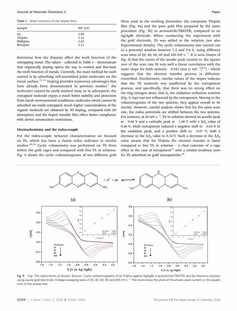
For the redox-couple behavior characterization we focusedon Th, which has been a classic redox indicator in similarstudies.28,34 Cyclic voltammetry was performed on Th fromwithin the gold cages and compared with free Th in solution.Fig. 9 shows the cyclic voltammograms of two different gold
films used as the working electrodes: the composite Th@Aufilm (Fig. 9a) and the pure gold film prepared by the sameprocedure (Fig. 9b) in acetonitrile/TBATFB, compared to anAg|AgBr electrode. When conducting the experiment withthe gold electrode, Th was added to the solution (see alsoExperimental details). The cyclic voltammetry was carried outin a potential window between 1.5 and 0.0 V, using differentscan rates of 20, 40, 60, 80 and 100 mV s�1. It is seen (insets ofFig. 9) that the curves of the anodic peak current vs. the squareroot of the scan rate fit very well a linear correlation with thesame slope for both systems �0.043 (mA (s mV�1)0.5) – whichsuggests that the electron transfer process is diffusion-controlled. Furthermore, similar values of the slopes indicatethat the Th molecule was unaffected by the entrapmentprocess, and specifically, that there was no strong effect onthe ring nitrogen atom, that is, the oxidation–reduction reaction(Fig. 9, top) was not influenced by the entrapment. Moving to thevoltammograms of the two systems, they appear overall to besimilar. However, careful analysis shows that for the same scanrate, the redox potentials are shifted between the two systems.For instance, at 20 mV s�1, Th in solution showed an anodic peakat �0.60 V and a cathodic peak at �1.06 V with a DEp value of0.46 V, while entrapment induced a negative shift to �0.65 V inthe oxidation peak, and a positive shift to �0.97 V, with adecrease in the DEp value to 0.34 V. Such a decrease in the DEp
value means that for Th@Au the electron transfer is fastercompared to free Th in solution – a clear outcome of a cageeffect in the case of entrapment35 with a similar tendency seenfor Th adsorbed on gold nanoparticles.36
Table 1 Work functions of the doped films
Sample WF (eV)
Au 5.00Th@Au 5.12RhB@Au 5.03BcG@Au 5.13
Fig. 9 Top: The redox forms of thionin. Bottom: Cyclic voltammograms of (a) Th@Au against Ag|AgBr in acetonitrile/TBATFB, and (b) thionin in solutionusing a pure gold electrode. Voltage sweeping rates of 20, 40, 60, 80 and 100 mV s�1. The insets show the plots of the anodic peak current vs. the squareroot of the sweep rate.
Journal of Materials Chemistry C Paper
This journal is©The Royal Society of Chemistry 2016 J. Mater. Chem. C, 2016, 4, 11548--11556 | 11555
Conclusions and outlook
We have developed an electroless methodology for incorporatingorganic molecules within conductive gold thin films. The typicaldopants entrapped in this article represent the large library oforganic molecules that can be incorporated into gold films,taking into account that the dopant properties influence themorphology and the properties of the resulting film. The non-trivial combination of entrapment of guest molecules within thegold film without hampering the conductivity properties of thefilm unravels the potential to use this film in electrochemicalmeasurements. The concept of one synthesis producing ametallic–organic hybrid electrode may be an alternative strategyfor the methods used today for surface modification of electrodes,such as the use of spacer bi-functional adsorbates37 and theutilization of layer by layer methods.38 This approach can savetime, eliminate the need for bi-functional reagents, removingthe requirement for an additional mediator to the analyzedsolution39 and enhancing the sensitivity of the electrode due tofaster electron transfer. We showed the principle of affectingand fine-tuning the metal’s work function; this is one of themost desired abilities in the field of optoelectronics and energyconversion – the full potential of this observation will beexplored in our labs.
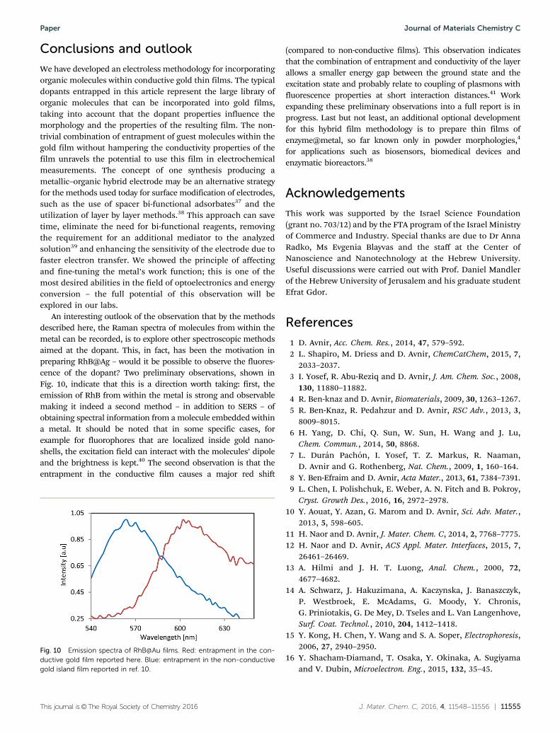
An interesting outlook of the observation that by the methodsdescribed here, the Raman spectra of molecules from within themetal can be recorded, is to explore other spectroscopic methodsaimed at the dopant. This, in fact, has been the motivation inpreparing RhB@Ag – would it be possible to observe the fluores-cence of the dopant? Two preliminary observations, shown inFig. 10, indicate that this is a direction worth taking: first, theemission of RhB from within the metal is strong and observablemaking it indeed a second method – in addition to SERS – ofobtaining spectral information from a molecule embedded withina metal. It should be noted that in some specific cases, forexample for fluorophores that are localized inside gold nano-shells, the excitation field can interact with the molecules’ dipoleand the brightness is kept.40 The second observation is that theentrapment in the conductive film causes a major red shift
(compared to non-conductive films). This observation indicatesthat the combination of entrapment and conductivity of the layerallows a smaller energy gap between the ground state and theexcitation state and probably relate to coupling of plasmons withfluorescence properties at short interaction distances.41 Workexpanding these preliminary observations into a full report is inprogress. Last but not least, an additional optional developmentfor this hybrid film methodology is to prepare thin films ofenzyme@metal, so far known only in powder morphologies,4
for applications such as biosensors, biomedical devices andenzymatic bioreactors.38
Acknowledgements
This work was supported by the Israel Science Foundation(grant no. 703/12) and by the FTA program of the Israel Ministryof Commerce and Industry. Special thanks are due to Dr AnnaRadko, Ms Evgenia Blayvas and the staff at the Center ofNanoscience and Nanotechnology at the Hebrew University.Useful discussions were carried out with Prof. Daniel Mandlerof the Hebrew University of Jerusalem and his graduate studentEfrat Gdor.
References
1 D. Avnir, Acc. Chem. Res., 2014, 47, 579–592.2 L. Shapiro, M. Driess and D. Avnir, ChemCatChem, 2015, 7,
2033–2037.3 I. Yosef, R. Abu-Reziq and D. Avnir, J. Am. Chem. Soc., 2008,
130, 11880–11882.4 R. Ben-knaz and D. Avnir, Biomaterials, 2009, 30, 1263–1267.5 R. Ben-Knaz, R. Pedahzur and D. Avnir, RSC Adv., 2013, 3,
8009–8015.6 H. Yang, D. Chi, Q. Sun, W. Sun, H. Wang and J. Lu,
Chem. Commun., 2014, 50, 8868.7 L. Duran Pachon, I. Yosef, T. Z. Markus, R. Naaman,
D. Avnir and G. Rothenberg, Nat. Chem., 2009, 1, 160–164.8 Y. Ben-Efraim and D. Avnir, Acta Mater., 2013, 61, 7384–7391.9 L. Chen, I. Polishchuk, E. Weber, A. N. Fitch and B. Pokroy,
Cryst. Growth Des., 2016, 16, 2972–2978.10 Y. Aouat, Y. Azan, G. Marom and D. Avnir, Sci. Adv. Mater.,
2013, 5, 598–605.11 H. Naor and D. Avnir, J. Mater. Chem. C, 2014, 2, 7768–7775.12 H. Naor and D. Avnir, ACS Appl. Mater. Interfaces, 2015, 7,
26461–26469.13 A. Hilmi and J. H. T. Luong, Anal. Chem., 2000, 72,
4677–4682.14 A. Schwarz, J. Hakuzimana, A. Kaczynska, J. Banaszczyk,
P. Westbroek, E. McAdams, G. Moody, Y. Chronis,G. Priniotakis, G. De Mey, D. Tseles and L. Van Langenhove,Surf. Coat. Technol., 2010, 204, 1412–1418.
15 Y. Kong, H. Chen, Y. Wang and S. A. Soper, Electrophoresis,2006, 27, 2940–2950.
16 Y. Shacham-Diamand, T. Osaka, Y. Okinaka, A. Sugiyamaand V. Dubin, Microelectron. Eng., 2015, 132, 35–45.
Fig. 10 Emission spectra of RhB@Au films. Red: entrapment in the con-ductive gold film reported here. Blue: entrapment in the non-conductivegold island film reported in ref. 10.
Paper Journal of Materials Chemistry C

11556 | J. Mater. Chem. C, 2016, 4, 11548--11556 This journal is©The Royal Society of Chemistry 2016
17 Y. Okinaka and M. Hoshino, Gold Bull., 1998, 31, 3–13.18 S. Hrapovic, Y. Liu, G. Enright, F. Bensebaa and J. H. T.
Luong, Langmuir, 2003, 19, 3958–3965.19 J. Turkevich, P. C. Stevenson and J. Hillier, Discuss. Faraday
Soc., 1951, 11, 55–75.20 J. Hu, W. Li, J. Chen, X. Zhang and X. Zhao, Surf. Coat.
Technol., 2008, 202, 2922–2926.21 ICDD – Card no. 01-071-4073.22 I. K. Suh, H. Ohta and Y. Waseda, J. Mater. Sci., 1988, 23,
757–760.23 R. C. Prince and G. N. George, Nat. Struct. Biol., 1997, 4, 247–250.24 W. Wang, W. Li, J. Ye and R. Zhang, J. Polym. Mater., 2010,
27, 351–357.25 S. Hou, J. Yan, Z. Hu and X. Wu, Chem. Commun., 2016, 52, 3–6.26 M. L. Tseng, C. M. Chang, B. H. Cheng, P. C. Wu, K. S.
Chung, M.-K. Hsiao, H. W. Huang, D.-W. Huang, H.-P.Chiang, P. T. Leung and D. P. Tsai, Opt. Express, 2013, 21,24460–24467.
27 D. Farin, A. Volpert and D. Avnir, J. Am. Chem. Soc., 1985,107, 3368–3370.
28 K. Hutchinson, R. E. Hester, W. J. Albery and A. R. Hillman,J. Chem. Soc., Faraday Trans. 1, 1984, 80, 2053–2071.
29 Y. Yuan, L. Ling, X. Wang, M. Wang, R. Gu and J. Yao,J. Raman Spectrosc., 2007, 38, 1280–1287.
30 W. Zhang and S. R. P. Silva, Carbon, 2010, 48, 2063–2071.31 B. De Boer, A. Hadipour, M. M. Mandoc, T. Van Wouden-
bergh and P. W. M. Blom, Adv. Mater., 2005, 17, 621–625.32 J. P. Hong, A. Y. Park, S. Lee, J. Kang, N. Shin and
D. Y. Yoon, Appl. Phys. Lett., 2008, 92, 20–23.33 S. Osella, D. Cornil and J. Cornil, Phys. Chem. Chem. Phys.,
2014, 16, 2866–2873.34 C. Dohno, E. D. A. Stemp and J. K. Barton, J. Am. Chem. Soc.,
2003, 125, 9586–9587.35 C. R. Raj, T. Okajima and T. Ohsaka, J. Electroanal. Chem.,
2003, 543, 127–133.36 Y. Ding, X. Zhang, X. Liu and R. Guo, Langmuir, 2006, 22,
2292–2298.37 D. D. Schlereth, E. Katz and H.-L. Schmidt, Electroanalysis,
1995, 7, 46–54.38 Y. M. Lvov, Z. Lu, J. B. Schenkman, X. Zu and J. F. Rusling,
J. Am. Chem. Soc., 1998, 120, 4073–4080.39 S. Liu, D. Leech and H. Ju, Anal. Lett., 2007, 36, 37–41.40 S. Zaiba, F. Lerouge, A. M. Gabudean, M. Focsan, J. Lerme,
T. Gallavardin, O. Maury, C. Andraud, S. Parola and P. L.Baldeck, Nano Lett., 2011, 11, 2043–2047.
41 A. Picot, F. Malvolti, B. Le Guennic, P. L. Baldeck, J. a G.Williams, C. Andraud and O. Maury, Inorg. Chem., 2007, 46,2659–2665.
Journal of Materials Chemistry C Paper