journal of luminescence - connecting repositories · 2017-04-23 · combustion synthesis phosphor...
TRANSCRIPT

Journal of Luminescence 134 (2013) 432–440
Contents lists available at SciVerse ScienceDirect
Journal of Luminescence
0022-23
http://d
n Corr
E-m
journal homepage: www.elsevier.com/locate/jlumin
Effect of NaF flux on microstructure and thermoluminescence properties ofSm3þ doped CdSiO3 nanophosphor
C. Manjunatha a,b,c, B.M. Nagabhushana a,b,n, D.V. Sunitha d, H. Nagabhushana d, S.C. Sharma d,G.B. Venkatesh e, R.P.S. Chakradhar f
a Department of Chemistry, M.S. Ramaiah Institute of Technology, Bangalore-560054, Indiab Visvesvaraya Technological University, Belgaum-590018, Indiac Department of Chemistry, R.V. College of Engineering, Bangalore-560059, Indiad Centre for Nano Research (CNR), Tumkur University, Tumkur-572103, Indiae Department of Chemistry, Central College, Bangalore University, Bangalore-560001, Indiaf CSIR-National Aerospace Laboratories, Bangalore-560017, India
a r t i c l e i n f o
Article history:
Received 23 May 2012
Received in revised form
8 July 2012
Accepted 2 August 2012Available online 10 August 2012
Keywords:
Silicates
Luminescence
Halide flux
Combustion synthesis
Phosphor
13/$ - see front matter & 2012 Elsevier B.V. A
x.doi.org/10.1016/j.jlumin.2012.08.006
esponding author. Tel.: þ91 9916030272.
ail address: [email protected] (B.M. Naga
a b s t r a c t
This work reports the preparation of CdSiO3:Sm3þ (1–7 mol%) nanophosphors by a low temperature
solution combustion method. For the first time the effect of NaF flux on the crystallization behavior,
morphology, and thermoluminescence property of 5 mol% Sm3þ doped CdSiO3 has been investigated.
The nanopowders are well characterized by powder X-ray diffraction (PXRD), Fourier Transform Infra-
Red (FT–IR), and scanning electron microscopy (SEM). PXRD results indicate that the powder calcined at
800 1C for 2 h has monoclinic phase. SEM results show that the powder is highly porous and the pore
size and shape can be modified by the addition of NaF flux. Addition of NaF could lead to formation of
particle type morphology and the increase in wt% of NaF changes crystallinity and phase. The
thermoluminescence glow curves for 2–6 wt% NaF in CdSiO3:Sm3þ show a single, well resolved glow
peak at 126, 130 and 150 1C, respectively. But for the sample prepared with 8 wt% of NaF flux shows
two glow peaks at 148 and 220 1C. With the addition of NaF flux, TL intensity can be effectively
enhanced.
& 2012 Elsevier B.V. All rights reserved.
1. Introduction
Over the last few years, rare earth ions doped inorganicnanomaterials have been particularly attractive because of theirunique luminescent properties [1,2]. It has been proved by manyresearchers that the luminescent properties of nanoscale materi-als are completely different from their bulk materials [3,4].Thermoluminescence (TL) is a well known phenomenon usedfor the dosimetry of ionizing radiations. The energy absorbed by aTL material during irradiation is released as visible and UV lighton subsequent heating of the sample. Many research groups haveshowed that the luminescent nanomaterials have potential appli-cations in dosimetry of ionizing radiations for the measurementsof high doses using TL technique, where the conventional micro-crystalline phosphors saturate [5–7]. The nanomaterials have alsoshowed the linearity in their TL responses in wide ranges ofexposures [8,9]. The increase in the number of surface states aswell as recombination charge carriers in nanomaterials may be
ll rights reserved.
bhushana).
the reason for their unique TL characteristics. Even thoughconsiderable amount of work has been done on TL of bulkmaterials, the TL properties of their nanocrystalline counterpartshave often not been reported. Therefore, the effort towardsimproving the TL characteristics are still being continued for thesame materials, either by synthesizing them at nano level bydifferent methods or by varying the dopant impurities [10,11] ordeveloping other new TL sensitive nanomaterials [12,13].
Silicate materials are useful in many applications of technolo-gical importance. Many metal silicates have been reported, andare being used in many areas: Mg2SiO4:Tb in thermolumines-cence dosimetry of the ionizing radiations [14], Gd2SiO5:Ce inscintillation phosphors because of their relatively high-density,good light output, and fast decay time [15]. Zn2SiO4:Mn was alsoused as the green component in the first tri-color lamp [16],CdSiO3 shows excellent phosphorescence property when dopedwith some transition metal and rare earth ions [17–19]. It isaccepted that Sm3þ ions in CdSiO3 host materials [18], can exhibitthe dominant pink emission peaks under near-UV excitation.Compared with other rare earth ions, the color-rendering indexon the proper host materials such as Ca3Y(VO4)3, CaF2, etc. dopedwith Sm3þ ions is higher [20,21]. Further, the morphology of

C. Manjunatha et al. / Journal of Luminescence 134 (2013) 432–440 433
phosphors (shape and size of the powder particles) is one of thekey parameters of their industrial application [22,23]. In order toobtain optimum emission characteristics for device applications,the characteristic features of host as well as concentration depen-dent studies of Sm3þ are essential.
In the present research work, we report Sm3þ doped CdSiO3
nanophosphors prepared by combustion route using oxalyldihy-drazide as a fuel followed by heat treatment at 800 1C for 2 h. Ingeneral, the preparation of metal silicates is a difficult process,because most of the silicates melt at very high temperature andappear in glassy and crystalline form. Conventionally, solid statediffusion methods have been used for the synthesis of silicates.Another technique, sol–gel synthesis, has also been used whichenables the preparation of fine, homogenous powders [24].Solution combustion synthesis is a successful, low-cost, timesaving method and has been effectively used for the preparationof a variety of industrially important materials [25]. The methodis based on the vigorous, spontaneous exothermic reactionbetween fuel and metal nitrate. This method has been adoptedto prepare many silicate materials, such as, CaSiO3, Zn2SiO4,which were used for various applications in phosphor industry,electrical insulators, pigments, glass ceramics, molecular sieves,zeolites, hybrid optics, bio ceramics etc. Wollastonite (CaSiO3)ceramics are generally used as a biomaterial in medical industryfor artificial bone and dental root because they show goodbioactivity and biocompatibility [26,27]. Therefore, we have alsofollowed solution combustion method and it has been discussedin detail in our previous report [28]. In the process of phosphorproduction, many flux materials were used to improve the bright-ness of spherical shape phosphor particles of micrometer size[29]. It plays an important role in controlling size, distributionand shape of phosphor particles [30]. Duault et al. have studiedthe effect of Li3PO4, Li2CO3, Na2CO3, K2CO3 flux on the morphol-ogy of LaPO4:Ce,Tb [23]. To the best of our knowledge, the effectof NaF flux addition on the crystallinity, microstructure andthermoluminescence properties of Sm3þ doped CdSiO3 phosphorhas not been reported so far. The thermoluminescent curves wereanalyzed by the glow peak shape method and the trap parameterssuch as activation energy (E), order of kinetics (b), and frequencyfactor (s) are estimated.
10 15 20 25 30 35 40 45 50 55 60 65 70
e
d
c
Inte
nsity
(a.u
)
b
2θ (degree)
a(001
) (201
)
(400
)(0
02) (-
202)
(-11
1) (202
) (310
)(-
311)
(311
)(1
12) (4
02)
(510
)(-
203)
(511
)
(-71
1)
(413
)
(712
)
Fig. 1. Powder XRD patterns of solution combustion derived Cd1�xSmxSiO3
samples (a) x¼0.00 (b) x¼0.01 (c) x¼0.03 (d) x¼0.05 and (e) x¼0.07 calcined
at 800 1C/2 h.
2. Experimental
2.1. Materials and synthesis
The chemicals, cadmium nitrate (Cd(NO3)2 �4H2O, 99.9%),samarium oxide (Sm2O3, 99.9%), fumed silica (SiO2, 99.9%, surfacearea 200 m2/g), and sodium fluoride (NaF, 99.9%) were used asanalytical reagents. Oxalyldihydrazide (ODH: C2H6N4O2) is usedas a fuel which was prepared in our laboratory; the detailedpreparation is given elsewhere [25]. CdSiO3:Sm3þ (1–7 mol%)nanophosphors was synthesized by combustion method followedby heat treatment at 800 1C for 2 h. Stoichiometric amount ofSm2O3 was taken in a 250 cm3 glass beaker and dissolved in asolution of dilute HNO3 (A.R.), and evaporated to dryness. Thecalculated amounts of cadmium nitrate, fumed silica and oxalyl-dihydrizide were added and dissolved in 50 cm3 de-ionizedwater. The mixture was stirred until a uniform and transparentsolution was obtained, and then gradually heated up in a pre-heated furnace at 500 1C, until it became sticky with the vaporiz-ing of water. Spontaneous ignition occurred, with the liberation oflarge volumes of gasses. The combustion was completed after afew seconds, and a foamy pale brown powder was obtained.Similar procedure was followed with different weights (2, 4, 6 and8 wt%) of NaF flux for the preparation of only 5 mol% Sm3þ doped
CdSiO3. The as-prepared CdSiO3:Sm3þ samples were annealed at800 1C for 2 h. The molar ratio of fuel to oxidizer was maintainedat 1 for all mixtures. No residual ODH and NO3
� was detected byIR spectroscopy after this post heat-treatment.
2.2. Characterization
The Powder X-ray diffraction (PXRD) measurements werecarried out on a Philips X’pert PRO PAnalytical X-ray diffract-ometer with graphite monochromatized Cu-Ka radiation source(l¼1.5418 A) operated at 40 kV and 30 mA. The XRD patternswere collected in the range of 101r2yr701. The morphologies ofthe phosphor powders were monitored by JEOL-JSM–6490 LVscanning electron microscope (SEM). The Fourier transform infra-red (FT-IR) spectra of the samples were measured using ShimadzuFT-IR infra-red spectrophotometer and the KBr pellet technique inthe range 4000–400 cm�1. UV–vis absorption of the sampleswas recorded on SL 159 ELICO UV–vis Spectrophotometer. Thethermoluminescence (TL) measurements were measured on amodel Nucleonix TL Reader, with a heating rate of 5 1C/s in thetemperature range of 40–400 1C. Before measurement, 100 mgpowder samples were pressed in to pellets (6 mm diameter and1 mm thickness), and then exposed to a standard UV lamp peak at254 nm with a power of 15 W. All measurements were carried outat room temperature.
3. Results and discussion
3.1. Powder X-ray diffraction analysis (PXRD)
Fig. 1 shows the powder X-ray diffraction patterns of theCdSiO3:Sm3þ (1–7 mol%) phosphors calcined at 800 1C for 2 h. Allthe diffraction peaks match very well with the standard valuesfrom the Joint Committee on Powder Diffraction Standards(JCPDS) data card No. 35–0810, which can be assigned to mono-clinic structure. Since the ionic radii of Sm3þ (rSm3þ ¼0.096 nm) isalmost similar to that of Cd2þ (r
Cd2þ ¼0.097 nm), it is expectedthat the Sm3þ ions can be easily occupied by the Cd2þsites inCdSiO3 host. Compared to solid-state reaction (1050 1C) andsol–gel approach (900 1C), it is obvious that the crystallinitytemperature of the samples prepared by this method is signifi-cantly lower (800 1C).

10 15 20 25 30 35 40 45 50 55 60 65 70
d
c
a
Inte
nsity
(a.u
)
b
2θ (degree)
JCPDS No : 35 - 0810
Fig. 2. Powder XRD patterns of NaF flux aided solution combustion derived
CdSiO3: Sm3þ (only 5 mol% ) samples calcined at 800 1C/2 h (a) no flux
(b) 2 wt% NaF (c) 4 wt% NaF and (d) 6 wt% NaF (The vertical line pattern
corresponds to standard PXRD pattern of monoclinic CdSiO3).
C. Manjunatha et al. / Journal of Luminescence 134 (2013) 432–440434
In order to identify the effect of flux on the phase formation ofthe sample, the PXRD analysis of the CdSiO3:Sm3þ sampleprepared with different wt% of NaF and the observed results areshown in Fig. 2. It is known that a flux in the process ofpreparation of phosphor contributes not only to the reaction ofceramic powders but also to the formation of a luminescentcenter in phosphors [31]. There is no effect on phase ofCdSiO3:Sm3þ (5 mol%) when the NaF flux used is just 2.0 wt%. Itis observed that the diffraction peak intensities slightly increasewith the dosage of NaF from 0 wt% to 2.0 wt%, which illustratesthat the flux can make the crystallinity of phosphor better.
We have also checked the effect of increase in the wt% of NaFon phase and crystallinity. It can be seen in the PXRD patternsobtained for 4.0 wt% and 6.0 wt% NaF (Fig. 2) that there is adecrease in the crystallinity and appearance of impurity peaks.The decrease in the crystallinity is due to appearance of highlycrystalline impurity phases. The highly dominating impuritypeaks at 2y¼23.62, 32.21, 33.27, and 49.50 can be ascribed toCd2SiO4 (JCPDS No: 85–0595) and at 2y¼34.84 and 39.1 are dueto appearance of small amounts Na4SiO4 (JCPDS No: 78-1432)phases along with CdSiO3 peaks, which are very less intense.These results are also consistent with the FT-IR analysis (whichwill be dealt with in subsequent sections) in which the sharpnessof peaks (639 and 680 cm�1) corresponding to Si–O stretchingfrequency is decreased. This fact implies that addition of 2.0 wt%of NaF flux is sufficient to obtain better crystallization and particlemorphology, further increase in its wt% leads to impurity phases.
3.2. Morphological analysis
The typical microstructure for CdSiO3:Sm3þ (5 mol%) nano-phosphor particles prepared without and with NaF flux (2 wt%and 4 wt%) is shown in Fig. 3. The scanning electron micrographshows that, the morphology of CdSiO3:Sm3þ powders preparedby combustion method without NaF flux is slightly different fromthose prepared with NaF flux. In general, the flux is used to act asa medium to incorporate the activators, reduce the firing tem-perature, and improve the crystallinity and morphology of therespective phosphors [32]. The pores and voids seen in Fig. 3A andB, are a result of large quantities of gases escaping duringcombustion reaction, which is a common feature of the materialsproduced by combustion synthesis. The effect of NaF flux on bothmorphology and particle size can be observed in the Fig. 3C and D.It is observed that the NaF flux plays a very important role in
changing the microstructure of the samples. The introduction ofNaF can lead to the formation of a liquid phase at a relatively lowtemperature. The liquid phase can considerably promote theformation of the phosphor with different morphologies. Porousnature of the microstructure changes to particles-type morphol-ogy (Fig. 3C). The particles combine with each other to form afused particle with increase in the quantity of NaF flux from 2 wt%to 4 wt% (Fig. 3D). The increase in wt% of NaF creates larger liquidphase, which suppresses the liberation of large quantity of gassesduring combustion. This causes the aggregation of particles in-toa larger one. Other parameters such as the melting and/or boilingpoints of this flux may also affect the formation and growthprocess of the particles [33]. These particles with the addition ofNaF prove to be highly crystalline, which is highly suitable tofabricate solid-lighting devices.
3.3. FT-IR spectral analysis
The FT-IR spectra of CdSiO3:Sm3þ (1–7 mol%) samples cal-cined at 800 1C for 2 h are shown in Fig. 4. It is observed that thebroad band from 840–1240 cm�1 is due to asymmetric stretchingvibration of Si–O–Si bond and stretching vibrations of terminalSi–O bonds. The peaks at 434–564 cm�1, 639 cm�1 and 680 cm�1
are the characteristic stretching vibrations of Si–O–Si bridges[26]. The sharp peak corresponding to 680 cm�1 can be ascribedto Si–O bond, which exists in the form of SiO3
2� . It can be noticedthat there is no change in the position or intensity of absorptionbands for the Sm3þ (1–7 mol%) doped CdSiO3 (Fig. 4), whichconfirms that the dopant has not altered its phase and crystal-linity. These results are consistent with those of PXRD results(Fig. 1). The small peak at 1655 cm�1 corresponding to CQObond, may be due to adsorbed CO2 in the sample during FT-IRmeasurements.
In order to understand the effect of NaF flux on the crystal-linity and phase of the CdSiO3:Sm3þ (5 mol%) sample, FT-IRanalysis was performed and is shown in Fig. 5. The intensity ofthe absorption band corresponding to 680 cm�1 decreases withincrease in the amount of NaF flux and finally disappears for6 wt%, which can be seen in the circled area of Fig. 5. It is alsonoted that the intensity of a strong absorption band at 639 cm�1
also decreases with increase in the NaF flux wt%. This may be dueto formation of impurity phases in which the Si–O bond exists inSiO4
2�. The above results are well supported by PXRD spectra(Fig. 2), which clearly tells the effect of flux on crystallinity andphase of the sample.
3.4. UV–vis absorption
Fig. 6 shows the UV–vis absorption spectra of Sm3þ doped (1–7 mol%) CdSiO3 phosphor calcined at 800 1C for 2 h. The absorp-tion spectrum reveals a peak around 230–270 nm which corre-sponds to oxygen to silicon (O–Si) ligand-to-metal charge-transfer (LMCT) in the SiO3
2� group [34]. The most commonlyused method to estimate the energy gap (Eg) is the Tauc relation[35] i.e., a(hv)¼K(hv�Eg)1/n , where ‘hv’ is the photon energy, ‘a’is the optical absorption coefficient, ‘K’ is constant and ‘n’ isindependent of the optical transition with an assigned value of2 and 1/2 for different allowed and indirect transitions respec-tively. The values of the optical band gaps of the un-doped andSm3þ doped CdSiO3 are obtained by plotting (aE)2 versus ‘E’ in thehigh-absorption range followed by extrapolating the linear regionof the plots to (aE)2
¼0 (Fig. 7). The analysis of the present dataindicates that the plots provide the linear relations, which can befitted with the above equation with n¼2 for both the un-dopedand Sm3þ doped samples. This indicates that the allowed directtransitions are responsible for the inter-band transitions in the

Fig. 3. SEM images of doped CdSiO3: Sm3þ (5 mol%) phosphors prepared with (A and B) no flux (C) 2.0 wt% NaF flux and (D) 4.0 wt% NaF flux.
400 800 1200 1600 2000 2400 2800 3200
e
1655 cm-1
d
639 cm-1
680 cm-1
% T
rans
mitt
ance
(a.u
)
b
c
434-564 cm-1
840-1240 cm-1
Wavenumber (cm-1)
a
Fig. 4. FT-IR spectra of Cd1�xSmxSiO3 samples calcined at 800 1C/2 h (a) x¼0.00
(b) x¼0.01 (c) x¼0.03 (d) x¼0.05 and (e) x¼0.07.
400 800 1200 1600 2000 2400 2800 3200
d
% T
rans
mitt
ance
(a.u
)
c
b
Wavenumber (cm-1)
a
Fig. 5. FT-IR spectra of 5 mol% Sm3þ doped CdSiO3 samples calcined at 800 1C/2 h
(a) No flux (b) 2 wt% NaF (c) 4 wt% NaF and (d) 6 wt% NaF.
C. Manjunatha et al. / Journal of Luminescence 134 (2013) 432–440 435
un-doped and the doped samples. The optical energy band gap forthe un-doped sample is found to be 5.33 eV and for the Sm3þ
doped (1–7 mol%) phosphors it varies between 5.45 and 5.62 eV(Fig. 7). It is noticed that the optical band gap is found to be lowerin the un-doped sample when compared to the Sm3þ doped
CdSiO3. To understand the effect of flux on the band gap, the UV–vis absorption spectra for Sm3þ (5 mol%) doped CdSiO3 preparedwith 2, 4, and 6 wt% NaF flux were measured and are shown in

200 250 300 350 400 450 500 550 600
a =undopedb =1 mol%c =3 mol%d =5 mol%e =7 mol%
Abs
orba
nce
(a.u
)
Wavelength (nm)
e
d
c
b
a
Fig. 6. UV–vis absorption spectra of Cd1�xSmxSiO3 samples calcined at 800 1C/2 h
(a) x¼0.00 (b) x¼0.01 (c) x¼0.03 (d) x¼0.05 and (e) x¼0.07.
2.0 2.5 3.0 3.5 4.0 4.5 5.0 5.5 6.0
(αhν
)2 (e
Vcm
-2)
e = 5.62 eVd = 5.58 eVc = 5.50 eVb = 5.45 eVa = 5.33 eV
ab
cd
e
Direct band gap Eg (eV)
E = hν(eV)
Fig. 7. Direct optical energy band gap of Cd1�xSmxSiO3 (a) x¼0.00, (b) x¼0.01, (c)
x¼03, (d) x¼0.05, and (e) x¼0.07.
200 250 300 350 400 450 500 550 600
Abs
orba
nce
(a.u
)
Wavelength (nm)
a = no flux
b = 2 wt%
c = 4 wt%
d = 6 wt%
a
d
b
c
Fig. 8. UV–vis absorption spectra of 5 mol% Sm3þ doped CdSiO3 samples calcined
at 800 1C/2 h (a) No flux (b) 2 wt% NaF (c) 4 wt% NaF and (d) 6 wt% NaF.
Fig. 9. Direct optical energy band gap of 5 mol% Sm3þ doped CdSiO3 samples
calcined at 800 1C/2 h (a) No flux (b) 2 wt% NaF (c) 4 wt% NaF and (d) 6 wt% NaF.
C. Manjunatha et al. / Journal of Luminescence 134 (2013) 432–440436
Fig. 8. It is noticed that the intensity of the absorption peak hasincreased slightly and has shifted to a higher wavelength regionfor 2 wt% NaF flux, as compared to that of the sample preparedwith no flux. With further increase in the wt% of NaF flux from4 to 6, the peak is shifted to a lower wavelength region. This maybe due to change in the phase and crystallinity of the samples.Fig. 9 shows the effect of different wt% of NaF on the direct bandgap for 5 mol% Sm3þ doped CdSiO3 sample. The direct band gapvalues for 2 wt% NaF flux used sample is slightly decreased due tochange in the morphology. For 4 and 6 wt% the values areunusually decreased as compared to that of 2 wt%, which maybe due to change in crystallinity and also due to mixed phase ofthe samples.
3.5. Thermoluminescence studies
The thermoluminescence (TL) glow curves were recorded foreach sample having different Sm3þ concentrations (1–7 mol %) inCdSiO3 host (without adding flux) irradiated by UV radiations for5 min. It is observed that well resolved glow peak at �173 1C wasrecorded at a heating rate of 5 1C s�1. There is no appreciable shiftin ‘Tm’ with Sm3þ concentration, but there is slight decrease in the
TL intensity on either sides of Sm3þ concentration. Fig. 10 showsthe TL intensity variation with Sm3þ concentration and is found tobe the highest for 5 mol% of Sm3þ in 5 min UV irradiation. In orderto study the effect of UV dose on the TL intensity of 5 mol% ofSm3þ doped CdSiO3, we have recorded the TL spectra for thesamples irradiated with UV for a prolonged time (3–20 min), andthey are shown in Fig. 11. A well resolved glow peak at �173 1Cwas recorded in all the UV irradiated samples. It is observed that,initially the glow curves are well defined for low UV irradiatedsamples (up to 10 min). However, with further increase in UVirradiation time (410 min) the glow curves are flat indicating theexistence of additional TL glow peaks.
The influence of different heating rates between 5–15 1C s�1
on TL response has been investigated on CdSiO3:Sm3þ (5 mol%:without flux) sample, irradiated with UV for 5 min and theobserved results are shown in Fig. 12. It is found that with
0 2 4 6 8 1025000
25500
26000
26500
27000
TL in
tens
ity (a
.u)
Sm3+ ion concentration (mol%)
Fig. 10. Variation of TL intensity with respect to Sm3þ concentration in CdSiO3
samples.
Fig. 11. TL glow curves of CdSiO3: Sm3þ (5 mol%) without NaF flux for different
UV dose.
0 50 100 150 200 250 3000
5000
10000
15000
20000
25000
TL
Inte
nsity
(a.u
)
Temperature (°C)
05°Cs-1
10°Cs-1
15°Cs-1
CdSiO3:Sm3+(5 mol%)
Fig. 12. TL glow curves of CdSiO3: Sm3þ (5 mol%) without NaF flux for different
heating rate for 10 min UV dose.
C. Manjunatha et al. / Journal of Luminescence 134 (2013) 432–440 437
increase in heating rates the TL peak intensity and area under thepeak are almost constant. However, peak temperature shiftstowards the higher temperature side. The glow peak (Tm) isshifted from 173 1C to 189 1C with increase of heating rate from5–15 1C s�1. The shifting of peak with increase in heating rate is aphenomenon frequently observed in the practice of TL; it isattributed to thermal quenching [36].
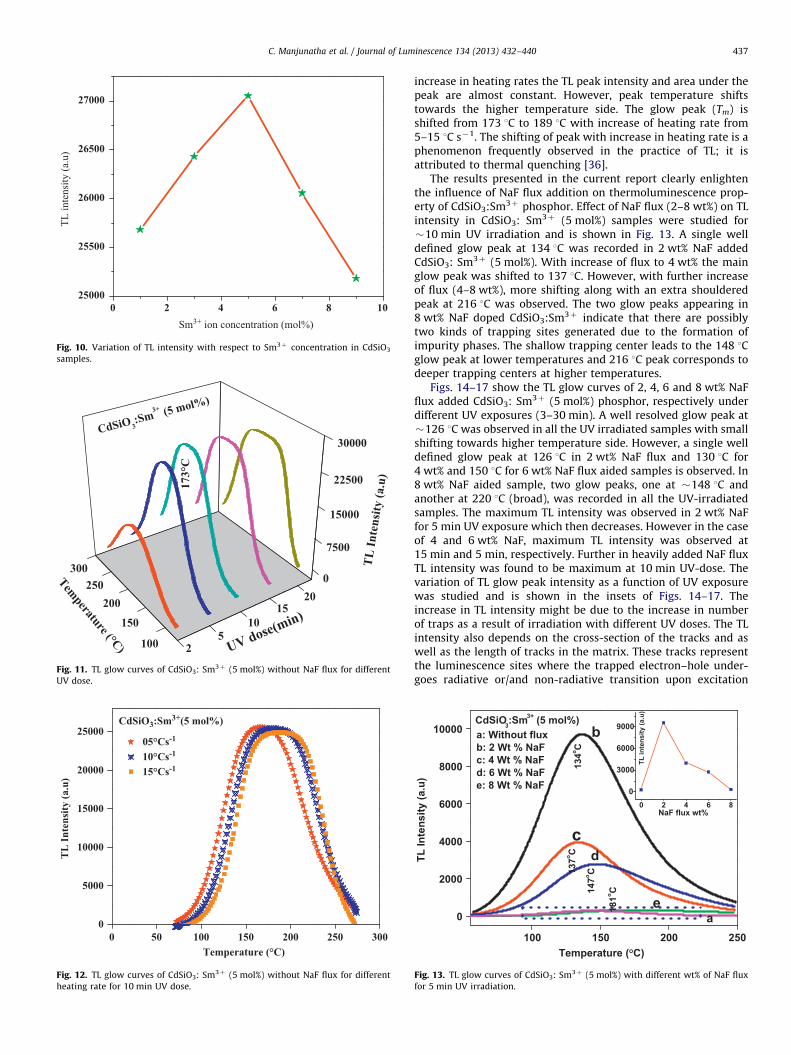
The results presented in the current report clearly enlightenthe influence of NaF flux addition on thermoluminescence prop-erty of CdSiO3:Sm3þ phosphor. Effect of NaF flux (2–8 wt%) on TLintensity in CdSiO3: Sm3þ (5 mol%) samples were studied for�10 min UV irradiation and is shown in Fig. 13. A single welldefined glow peak at 134 1C was recorded in 2 wt% NaF addedCdSiO3: Sm3þ (5 mol%). With increase of flux to 4 wt% the mainglow peak was shifted to 137 1C. However, with further increaseof flux (4–8 wt%), more shifting along with an extra shoulderedpeak at 216 1C was observed. The two glow peaks appearing in8 wt% NaF doped CdSiO3:Sm3þ indicate that there are possiblytwo kinds of trapping sites generated due to the formation ofimpurity phases. The shallow trapping center leads to the 148 1Cglow peak at lower temperatures and 216 1C peak corresponds todeeper trapping centers at higher temperatures.
Figs. 14–17 show the TL glow curves of 2, 4, 6 and 8 wt% NaFflux added CdSiO3: Sm3þ (5 mol%) phosphor, respectively underdifferent UV exposures (3–30 min). A well resolved glow peak at�126 1C was observed in all the UV irradiated samples with smallshifting towards higher temperature side. However, a single welldefined glow peak at 126 1C in 2 wt% NaF flux and 130 1C for4 wt% and 150 1C for 6 wt% NaF flux aided samples is observed. In8 wt% NaF aided sample, two glow peaks, one at �148 1C andanother at 220 1C (broad), was recorded in all the UV-irradiatedsamples. The maximum TL intensity was observed in 2 wt% NaFfor 5 min UV exposure which then decreases. However in the caseof 4 and 6 wt% NaF, maximum TL intensity was observed at15 min and 5 min, respectively. Further in heavily added NaF fluxTL intensity was found to be maximum at 10 min UV-dose. Thevariation of TL glow peak intensity as a function of UV exposurewas studied and is shown in the insets of Figs. 14–17. Theincrease in TL intensity might be due to the increase in numberof traps as a result of irradiation with different UV doses. The TLintensity also depends on the cross-section of the tracks and aswell as the length of tracks in the matrix. These tracks representthe luminescence sites where the trapped electron–hole under-goes radiative or/and non-radiative transition upon excitation
Fig. 13. TL glow curves of CdSiO3: Sm3þ (5 mol%) with different wt% of NaF flux
for 5 min UV irradiation.

Fig. 14. TL glow curves of 2 wt% NaF in CdSiO3: Sm3þ (5 mol%) with TL intensity
for different UV irradiation (3–30 min). (Inset shows variation of TL intensity vs.
UV dose).
Fig. 15. TL glow curves of 4 wt% NaF in CdSiO3: Sm3þ (5 mol%) with TL intensity
for different UV irradiation (3–25 min). (Inset shows variation of TL intensity vs.
UV dose).
Fig. 16. TL glow curves of 6 wt% NaF in CdSiO3: Sm3þ (5 mol%) with TL intensity
for different UV irradiation (3–25 min). (Inset shows variation of TL intensity vs.
UV dose).
Fig. 17. TL glow curves of 8 wt% NaF in CdSiO3: Sm3þ (5 mol%) with TL intensity
for different UV irradiation (3–25 min). (Inset shows variation of TL intensity vs.
UV dose).
C. Manjunatha et al. / Journal of Luminescence 134 (2013) 432–440438
with a suitable source. In nanophosphor, since the surface tovolume ratio increases significantly, it helps in the formation ofdifferent types of traps upon UV irradiation. The electrons andholes are expected to be trapped at tracks of different depth.Therefore, the trapped carriers at the surface states are releasedby heating the sample and they recombine with each other andgive out luminescence which is known as thermoluminescence.In nanomaterials the length of such a track may be a few tens ofnanometers, so the number of trap centers or luminescencecenters will be less for lower doses. Similar observation wasreported in various nanophosphors by different authors [37,38].If the deep traps are present or formed at heavy dose irradiationinside the hosts of the nanomaterials, they may not be ableto show TL emissions due to re-trapping within the deep trap.The emitted photons from the deep traps might get self-absorbedwithin the deep trap due to the presence of some meta stableenergy levels within the track and photons may not reach tothe TL detector. Therefore the saturation effects or decrease in theTL intensity is expected at higher UV doses.
In the present study it is observed that, if we increase the dose,more overlapped tracks are expected in the matrix, as a result ofwhich saturation/decrease of TL intensity occurs. Thus on increas-ing the dose, a large number of surface defects are produced in thenanoparticles which ultimately keep on increasing with the dosetill saturation is achieved [39]. The luminescent property of thephosphors arises from the complex interaction among host struc-ture, activators, and defects. The charge unbalance and latticedistort could induce point defects in the structure, which wouldincrease the non-radiative process that resulted in the reduction ofluminescence intensity. As observed in Fig. 13, with the variation inthe TL intensity of 5 mol% Sm3þ doped CdSiO3 prepared withdifferent wt% of NaF fluxes one can predict that it might be due tothe formation of various types of traps and lattice defects. The ionicradius of Sm3þ ion (0.096 nm) is much closer to Cd2þ ions(0.097 nm) than to that of Si4þ ions (0.041 nm). In CdSiO3:Sm3þ
phosphors, the trivalent Sm3þ ions are substituted for Cd2þ ions,which induced the charge unbalance. The substitution of Sm3þ
may lead to charge imbalance (2Sm3þ–2Cd2þ-two holes) or

Table 1Estimated trap parameters for addition of NaF flux (2–8 wt%) in CdSiO3: Sm3þ
(5 mol%).
NaF Flux
(wt%)
Peak Tm
(1C)
Order of
kinetics, b (mg)
Activation energy
(eV)
Frequency
factor, s (s�1)
Et Ed Eo Eave
Without
flux
1 104 2(0.50) 0.69 0.73 0.71 0.71 6Eþ10
2 142 2(0.51) 0.87 0.89 0.88 0.88 9Eþ11
3 167 2(0.49) 0.81 0.86 0.84 0.83 5Eþ10
4 196 2(0.48) 0.49 0.58 0.54 0.54 4Eþ06
2 1 091 2(0.50) 1.05 1.04 1.05 1.05 9Eþ15
2 129 2(0.49) 0.82 0.86 0.84 0.84 6Eþ11
3 143 2(0.50) 0.56 0.62 0.59 0.59 2Eþ08
4 184 2(0.50) 0.41 0.50 0.45 0.45 6Eþ05
4 1 090 2(0.48) 1.09 1.09 1.09 1.09 4Eþ16
2 127 2(0.49) 0.85 0.88 0.87 0.87 2Eþ12
3 137 2(0.48) 0.59 0.66 0.63 0.63 6Eþ08
4 190 2(0.48) 0.26 0.37 0.31 0.31 1Eþ04
6 1 098 2(0.50) 0.61 0.65 0.64 0.63 7Eþ09
2 121 2(0.52) 1.56 1.39 1.47 1.48 3Eþ20
3 140 2(0.50) 0.72 0.76 0.74 0.74 1Eþ10
4 196 2(0.49) 0.43 0.52 0.47 0.47 8Eþ05
8 1 121 2(0.51) 0.51 0.56 0.54 0.54 8Eþ07
2 137 2(0.51) 0.85 0.87 0.86 0.86 6Eþ11
3 172 2(0.51) 0.82 0.86 0.84 0.84 5Eþ10
4 210 2(0.50) 1.36 1.36 1.37 1.36 3Eþ15
C. Manjunatha et al. / Journal of Luminescence 134 (2013) 432–440 439
point defect (2Sm3þ–3Cd2þ-one vacant site of Cd2þ), which areplaying a major role in luminescence process. The TL intensity andits position of UV irradiated CdSiO3:Sm3þ sample are attributed tothe defects corresponding to uneven dopant substitution. However,the TL glow curves of CdSiO3:Sm3þ (5 mol%) sample prepared withdifferent wt% of NaF flux (Fig. 13) appear to be same barring thevariation in their intensities. The enhancement in the TL intensitymight be due to the incorporation of Naþ and F� ions whichequalize the charge unbalance generated by Sm3þ substitution forCd2þ , and thus reduce the lattice distort and enhance the lumi-nescent intensity. Further increase in the NaF content (42 wt%)could lead to decrease in the TL intensity, which might be due tothe change in crystal structure and lattice parameters (Fig. 2). Incontrast, the larger lattice distortion might be induced when 8 wt%of NaF was introduced to the host lattice, which would decreasethe luminescent intensity of the phosphors. Therefore, 2 wt% NaFions might be the optimal flux and charge compensator for theCdSiO3:Sm3þ (5 mol%) phosphors. The variation in the TL intensitywith the UV dose for the 2–8 wt% NaF flux aided 5 mol% Sm3þ
doped CdSiO3 (Figs. 14–17) is predicted to be due to competition/overlapping of electron–hole transition upon heating. This uneven-ness in TL response is due to various types of traps/defects formeddue to the reduction in the particle size, non-equivalent ionsubstitution, different wt% of NaF content (charge compensator),destruction of actual crystal structure, and mixed/impurity phases.
4. Calculation of kinetic parameters
The glow curve is related to the trap levels that lie at differentdepths in the band gap between the conduction and the valencebands of CdSiO3. These trap levels are characterized by differentkinetic parameters. Kinetic parameters of trap levels are reportedby various methods. Many of them are based on the observationof thermally stimulated relaxation spectra, i.e. TL spectra. Weemployed the Peak Shape (PS) method, which is generally calledas Chen’s [40] method, to determine the kinetic parameters of theglow peak of the of NaF flux aided CdSiO3:Sm3þ (5 mol%) sample.The peak shape method is mainly used to calculate the order ofkinetics. Order of kinetics can be evaluated from the symmetry
factor (mg) of the glow peak and it is calculated using [41] Eq. (1).
mg ¼ ðT22TmÞ=ðT22T1Þ ð1Þ
where, T1, Tm and T2 represent the temperature of half-intensity at low-temperature side, peak temperature and tem-perature of half-intensity at high-temperature side of TL peak,respectively. It is found that the geometrical factor (mg)�equal to0.31, seems to be unrealistic because the values lie in between0.42 and 0.52. The unexpected value of ‘mg’ led us to speculatethat this peak may be comprised of more than one peak having aclose trap distribution, which is superimposed giving rise to abroad TL glow curve. This encouraged us to make use of the curvefitting technique to analyze the glow curve. The TL glow curve isfirst deconvoluted based on Gaussian function and then westudied the individual deconvoluted peak. Activation energy (E)was calculated by using the Chen’s equations, which gives thetrap depth in terms of t, d, o. A general formula for ‘E’ was givenby Eq. (2).
E¼ Cg kTm2=g
� �2bgð2kTmÞ ð2Þ
where g is t, d, or o. The values of t, d, and o are respectivelydetermined by low-temperature half-width (t¼Tm�T1), high-temperature half-width (d¼T2�Tm) and full width (o¼T2�T1),and k is the Boltzmann constant. Therefore, according to Eq. (2),different values of ‘E’ remarked as Et, Ed and Eo can be obtainedwhen g is t, d, or o, respectively. For example, if g stands for t, thenCt¼1.51þ3.0(mg-0.42), bt¼1.58þ4.2(mg-0.42), Et¼1.51(kTm
2 /t)–1.58(2 kTm); if g stands for d, then Cd¼0.976þ7.3(mg-0.42), bd¼0,Ed¼0.976(kTm
2 /d)–0(2 kTm); if g stands for o, then Co¼2.52þ10.2(mg-0.42), bo¼1.0, Eo¼2.52(kTm
2 /o)–1.0(2 kTm). The value offrequency factor (s) can be obtained with the following equation[15]
bE
KT2m
¼ s exp�E
KTm
� �1þðb�1ÞDm
� �ð3Þ
where b is the linear heating rate, b is the order of kinetics and
Dm ¼2KTm
E
Several authors have even reported similar studies for evalua-tion of kinetic parameters using Chen’s peak shape methodapplied directly to the peaks which were deconvoluted usingOrigin 6.1 software without using any Glow curve de-convolution(GCD) functions [42]. The estimated peak parameters forCdSiO3:Sm3þ (5 mol%) prepared without and with 2–8 wt% ofNaF flux estimated are given in Table 1. The values of ‘E’ werefound to be in the range of 0.31–1.48 eV. This wide range mightbe due to the existence of both shallow traps and deep trapswhich have been observed in several nanomaterials [43]. Themean activation energy and the frequency factors for the 2 wt%NaF flux aided sample are found to be 1.05 eV, 9�1015 Hz and0.45 eV, 6�1005 Hz pertaining to the glow curves with peaks at91 1C and 184 1C respectively. The lower activation energy(0.45 eV) corresponding to higher temperature peak (184 1C)and higher activation energy (1.05 eV) corresponding to lowertemperature peak (91 1C) is attributed to the complex nature ofpeaks. Sunta et al. discussed the limitation of peak shape methodfor the calculation of ‘E’ of TL glow peaks. The limitation of thepeak shape method is not because of the improper application ofthe methods, but is for reasons inherent in the shape of the peakitself. High values of d, t and o together with low value of ‘Tm’lead to a lower value of ‘E’ [44].
5. Conclusions
In summary, NaF flux aided solution combustion method hasbeen followed to prepare CdSiO3:Sm3þ nanocrystalline phosphors.The effect of NaF flux content on the crystal structure, morphology

C. Manjunatha et al. / Journal of Luminescence 134 (2013) 432–440440
and luminescent properties is investigated. PXRD and SEM studiesreveal that 2 wt% NaF flux addition has significantly improved thecrystallinity, reduced agglomeration of the particle without alteringthe monoclinic phase. With a further increase in NaF content(4–8 wt%), the crystallinity is decreased and formation of Cd2SiO4
phase was observed. The optical energy band gap for the un-dopedand Sm3þ doped (1–7 mol%) phosphors was estimated and found tobe 5.33 eV and for the Sm3þ doped (1–7 mol%) phosphors it variesbetween 5.45 and 5.62 eV. It is noticed that the optical band gap isfound to be lower in the un-doped sample when compared to theSm3þ doped CdSiO3. It is observed that, the absorption bandsshifted in 8 wt% NaF flux, which might be attributed to phasechange from CdSiO3 to Cd2SiO4. The thermoluminescence (TL) glowcurves for 2–6 wt% NaF in CdSiO3 show a single well resolved glowpeak at 126, 130 and 150 1C respectively. However, in 8 wt% NaFadded samples two glow peaks appear at �148 1C and 220 1Crespectively. With the addition of NaF flux, TL intensity can beenhanced effectively. The keen observation of our present workindicates that the addition of 2 wt% NaF flux during the preparationof Sm3þ doped CdSiO3 is highly useful in enhancing its crystallinity,morphology and very importantly the thermoluminescence intensity.
Acknowledgments
The author C. Manjunatha is grateful to the Management,Principal, Vice-principal and Head of the Department of Chem-istry of R.V. College of Engineering, Bangalore, for their constantsupport and encouragement. Dr. B.M.N gratefully acknowledgesVisvesvaraya Technological University, Belgaum for the financialsupport (VTU/Aca./2009-10/A-9/11714) extended to carry out thisresearch work.
References
[1] X. Zhang, J. Zhang, Z. Nie, M. Wang, X. Ren, X. Wang, Appl. Phys. Lett. 90(2007) 151911.
[2] G. Jia, H. You, Y. Song, J. Jia, Y. Zheng, L. Zhang, K. Liu, H. Zhang, Inorg. Chem.48 (2009) 10193.
[3] N. Salah, P.D. Sahare, A.A. Rupasov, J. Lumin. 124 (2006) 357.[4] N. Salah, P.D. Sahare, S.P. Lochab, P. Kumar, Radiat. Meas. 41 (2006) 40.[5] E. Dela Rosa, R.A. Rodriguez, R. Melendrez, P. Salas, L.A. Diaz-Torres,
M. Barboza-Flores, Nucl. Instrum. Methods B 255 (2007) 357.[6] V. Kumar, R. Kumar, S.P. Lochab, N. Singh, Radiat. Eff. Defects Solids 161
(2006) 479.[7] A. Pandey, P.D. Sahare, J.S. Bakare, S.P. Lochab, F. Singh, D. Kanjilal, J. Phys. D
Appl. Phys. 36 (2003) 2400.
[8] P.D. Sahare, R. Ranjan, N. Salah, S.P. Lochab, J. Phys. D: Appl. Phys 40 (2007) 759.[9] S.P. Lochab, P.D. Sahare, R.S. Chauhan, N. Salah, R. Ranjan, A. Pandey, J. Phys.
D:Appl. Phys. 40 (2007) 1343.[10] A.R. Lakshmanan, M.T. Jose, V. Ponnusamy, P. Kumar, R. Vivek, J. Phys. D:
Appl. Phys. 35 (2002) 386.[11] S.S. Shinde, B.S. Dhabekar, T.K. Gundu Rao, B.C. Bhatt, J. Phys. D: Appl. Phys.
34 (2001) 2683.[12] S. Bangaru, G. Muralidharan, Nucl. Instrum. Meth. B 268 (2010) 1653.[13] J. Marcazzo, M. Santiago, C. D’Angelo, C. Furetta, E. Caselli, Nucl. Instrum.
Meth. B 268 (2010) 183.[14] T. Hashizume, Y. Kato, T. Nakajima, T. Tovya, H. Sakamato, N. Kotera, S.
Iguchi, in: Proceedings of the IAEA Symposium on Advanced RadiationDetectors, Vienna, 1971, p. 91.
[15] D.W. Cooke, B.L. Bennett, R.E. Muenchausen, K.J. McClellan, J.M. Roper,M.T. Whittaker, J. Appl. Phys. 86 (1999) 5308.
[16] H.H. Haft, W.A. Thornton, Journal of Indo-European Studies (1972).[17] J. Kuang, Y. Liu, Chem. Phys. Lett. 424 (2006) 58.[18] B. Lei, Y. Liu, J. Liu, Z. Ye, C. Shi., J. Solid State Chem. 177 (2004) 1333.[19] X. Qu, L. Cao, W. Liu, G. Su, C. Xu, P. Wang, J. Alloys Compd. 494 (2010) 196.[20] Vengala Rao Bandi, Bhaskar Kumar Grandhe, M. Jayasimhadri, Kiwan Jang,
Ho-Sueb Lee, Soung-Soo Yi, Jung-Hyun Jeong, J. Cryst. Growth 326 (2011)120.
[21] G. Lakshminarayana, R. Yang, M. Mao, J. Qiu, I.V. Kityk, J. Non-Cryst. Solids355 (2009) 2668.
[22] Y.C. Kang, E.J. Kim, D.Y. Lee, H.D. Park, J. Alloys Compd. 347 (2002) 266.[23] F. Duault, M. Junker, P. Grosseau, B. Guilhot, P. Iacconi, B. Moine, Powder
Technol. 154 (2005) 132.[24] T.S. Ahmadi, M. Haase, H. Weller, Mater. Res. Bull. 35 (2000) 1869.[25] K.C. Patil, M.S. Hegde, T. Rattan, S.T. Aruna, Chemistry of Nanocrystalline
Oxide materials, Combustion Synthesis, Properties and Applications, WorldScientific Publishing Co. Pvt. Ltd, Singapore, 2008.
[26] R.P.S. Chakradhar, B.M. Nagabhushna, G.T. Chandrappa, K.P. Ramesh, J.L. Rao,Mater. Chem. Phys. 95 (2006) 169.
[27] R.P.S. Chakradhar, B.M. Nagabhushana, G.T. Chandrappa, K.P. Ramesh,J.L. Rao, J. Chem. Phys. 121 (2004) 10250.
[28] C. Manjunatha, D.V. Sunitha, H. Nagabhushana, B.M. Nagabhushana,S.C. Sharma, R.P.S. Chakradhar, Spectrochim. Acta A 93 (2012) 140.
[29] F. Bondioli, A.B. Corradi, T. Manfredini, Chem. Mater. 12 (2) (2002) 324.[30] D. Haranath, P. Sharma, H. Chander, A. Ali, N. Bhalla, S.K. Halder, Mater.
Chem. Phys. 101 (2006) 163.[31] G. Li, Y. Lai, T. Cui, H. Yu, D. Liu, S. Gan, Mater. Chem. Phys. 124 (2010) 1094.[32] C.L. Lo, J.G. Duh, B.S. Chiou, C.C. Peng, L. Ozawa, Mater. Chem. Phys. 71 (2001) 179.[33] H.I. Won, H.H. Nersisyan, C.W. Won, K.H. Lee, Mater. Chem. Phys. 129 (2011) 955.[34] S. Atalay, H.I. Adiguzel, F. Atalay, Mater. Sci. Eng. A 304-306 (2001) 796.[35] X. Liu, F. Zhou, M. Gu, S. Huang, B. Liu, C. Ni, Opt. Mater. 31 (2008) 126.[36] G. Sharma, S.P. Lochab, N. Singh, J. Alloys Compd. 501 (2010) 190.[37] G. Sharma, S.P. Lochab, N. Singh, Curr. Appl. Phys. 11 (2011) 921.[38] A. Vij, S.P. Lochab, S. Singh, R. Kumar, N. Singh, J. Alloys Compd. 486 (2009)
554.[39] N. Salah, Rad. Phys. Chem. 80 (2011) 1.[40] R. Chen, Y. Kirish, Analysis of Thermally Stimulated Proceses, Pergamon,
NewYork, 1981.[41] S.W.S. Mckeever, Thermoluminescence of Solids, in: G.G. Chai, F. Wu,
S.T. Wang (Eds.), Atomic Energy Press, Chin., 1993.[42] G. Kittis, J.M. Gomz-Ross, J.W.N. Tuyn, J. Phys. D: Appl. Phys. 31 (1998) 2636.[43] N. Salah, P.D. Sahare, A.A. Rupasov, J. Lumin. 124 (2007) 357.[44] C.M. Sunta, Feria, W.E. Ayta, T.M. Piters, S. Watanabe, Radiat. Meas. 30 (1999) 197.