jn516x jtag debugging in beyondstudio · jn516x jtag debugging in beyondstudio this application...
TRANSCRIPT

Application Note: JN-AN-1203 JN516x JTAG Debugging in BeyondStudio
This Application Note describes how to use the JTAG debugging features of the NXP JN516x wireless microcontrollers using the “BeyondStudio for NXP” software tool. JTAG debugging is demonstrated using an IEEE802.15.4 application running on components of the NXP JN516x-EK001 Evaluation Kit.
1 Application Overview This Application Note describes the use of “BeyondStudio for NXP” for the JTAG debugging of applications running on NXP JN516x wireless microntrollers. BeyondStudio for NXP is an Eclipse-based Integrated Devleopment Environment (IDE) that allows the user to write, build and debug applications for the JN516x devices. It has the part number JN-SW-4141 and can be obtained free-of-charge via the NXP Wireless Connectivity TechZone. The installation and general use of this software tool is fully described in the BeyondStudio for NXP Installation and User Guide (JN-UG-3098), which is available from the TechZone.
BeyondStudio for NXP can be used with a number of wireless network protocols supported on the JN516x devices (the relevant protocols are indicated on the TechZone). In this Application Note, the IEEE802.15.4 Home Sensor Demonstration application is used, which is run on components of the JN516x-EK001 Evaluation Kit. The hardware and software required to use this Application Note are summarised in the next section.
2 Pre-requisites In order to use this Application Note, you will need the following hardware and software.
2.1 Hardware Requirements • NXP JN516x-EK001 Evaluation Kit
• NXP DR1222 JTAG Expansion Board (see section 9 for schematics)
• JTAG adaptor/dongle (Beyond Debug Key, or Amontec JTAGkey or JTAGkey2)
You will also need a USB cable for connecting the JTAG adaptor to your PC.
2.2 Software Requirements • BeyondStudio for NXP (JN-SW-4141)
• JN516x IEEE802.15.4 Software Developer’s Kit (JN-SW-4163)
• 802.15.4 Home Sensor Demonstration for JN516x Application Note (JN-AN-1180)
The above software components are available via the IEEE802.15.4 tab on the TechZone. You must install JN-SW-4141 and JN-SW-4163 on your development PC as described in the BeyondStudio for NXP Installation and User Guide (JN-UG-3098). The Application Note JN-AN-1180 must then be installed in your BeyondStudio for NXP workspace.
JN-AN-1203 (v1.2) 27-Feb-2015 © NXP Laboratories UK 2015 1
JN516x JTAG Debugging in BeyondStudio
3 Compatibility The software descriptions in this Application Note relate to the following evaluation kit and SDK (Software Developer’s Kit) versions:
Product Type Part Number Version Evaluation Kit JN516x-EK001 - SDK Libraries JN-SW-4163 v1052 SDK Toolchain JN-SW-4141 v1111
4 Application Set-up This Application Note uses the IEEE802.15.4 Home Sensor Demonstration application (JN-AN-1180) as a vehicle for introducing JTAG debugging. The End Device application will be debugged from BeyondStudio for NXP while the Coordinator is run in normal mode.
Note: The JN-AN-1180 documentation describes the demonstration as using three End Device nodes. Here, we will only use one End Device node, as well as the Coordinator node.
Start BeyondStudio for NXP and import the IEEE802.15.4 Home Sensor Demonstration project – instructions are provided in the JN-AN-1180 documentation. Then set up the Coordinator and End Device, as described below.
4.1 Coordinator Set-up In this Application Note, the Coordinator will be used in normal mode. Assemble the Coordinator node from the following JN516x-EK001 Evaluation Kit components:
• DR1174 Carrier Board
• DR1215 LCD Expansion Board
• JN5168 module
Connect the carrier board to your PC using a 'USB A to Mini B' cable from the evaluation kit.
The Coordinator application now needs to be built and programmed into the JN5168 module on this board, as described below.
4.1.1 Build the Application To build the Coordinator application, first ensure that the project is highlighted in the left Project Explorer pane of BeyondStudio and use the drop-down list associated with the Build button on the toolbar to select the relevant build configuration – AN1180_154_HomeSensorCoord. The application will now be built and a binary file will be created in the Build directory for the application, the resulting filename indicating both the chip type (e.g. JN5168) and networking stack (154 for 802.15.4) for which it was built.
4.1.2 Load the Application Binary Load the Coordinator application binary into the JN516x device using the Flash programmer tool within BeyondStudio for NXP, as described in the BeyondStudio for NXP Installation and User Guide (JN-UG-3098). Once programmed, this board must be reset, after which it will display the NXP logo and a menu on its LCD screen.
2 © NXP Laboratories UK 2015 JN-AN-1203 (v1.2) 27-Feb-2015

JN516x JTAG Debugging in BeyondStudio
4.2 End Device Set-up Assemble the End Device node from the following JN516x-EK001 Evaluation Kit components:
• DR1174 Carrier Board
• JN5168 module
Do not fit the JTAG Expansion Board yet. Connect the carrier board to your PC using a 'USB A to Mini B' cable from the evaluation kit.
The End Device application now needs to be built and programmed into the JN5168 module on this board, and the board must also be enabled for JTAG debugging, as described below.
4.2.1 Build the Application When using JTAG debugging, a flag must be set in the application binary header which instructs the bootloader to enable the JTAG port. The JTAG port may also be configured via a second flag to use the pins allocated to UART0, or to UART1 on the JN516x device. These flags are set via directives in the application Makefile. When using the DR1222 JTAG Expansion Board on a DR1174 Carrier Board, the JTAG header is connected to the UART0 pins.
In the Project Explorer pane, open the End Device application’s Makefile by following the path AN1180_154_HomeSensorEndD>Build and double-clicking on Makefile.
To build the application for JTAG debugging on the UART0 pins, uncomment this line in the Makefile: # Debug options define DEBUG for HW debug DEBUG ?= HW But leave this line set to UART0: # Define which UART to use for debug DEBUG_PORT ?= UART0 The End Device must now be built using this configuration.
To build the End Device application, first ensure that the project is highlighted in the left Project Explorer pane of BeyondStudio and use the drop-down list associated with the Build button on the toolbar to select the relevant build configuration – AN1180_154_HomeSensorEndD. The application will now be built and a binary file will be created in the Build directory for the application, the resulting filename indicating both the chip type (e.g. JN5168) and networking stack (154 for 802.15.4) for which it was built. Binary files built for JTAG debugging contain an additional _hwdbg component in the filename.
4.2.2 Load the Binary File Once the End Device application has been built for JTAG debugging, the resulting binary file must be programmed into the JN516x device on the relevant board using the integrated Flash programmer tool. This file contains instructions to enable the JTAG interface and not the actual application code, which will be loaded into the device later via the JTAG interface.
Load the JTAG-enabled binary file AN1180_154_HomeSensorEndD_JN5168_hwdbg.bin into the JN516x device using the Flash programmer tool within BeyondStudio for NXP, as described in the BeyondStudio for NXP Installation and User Guide (JN-UG-3098).
Once this file has been programmed, the JTAG pins are enabled for debugging and the hardware can now be reconfigured for debugging, as described in the next section.
JN-AN-1203 (v1.2) 27-Feb-2015 © NXP Laboratories UK 2015 3

JN516x JTAG Debugging in BeyondStudio 4.2.3 Configure Hardware for JTAG Debugging Disconnect the USB cable from the End Device carrier board.
On the DR1174 Carrier Board, there is a jumper labelled JTAG. This jumper is normally configured in the “DIS” position. Remove the jumper and re-connect it in the “EN” position (see below). This remaps the UART0 pins from the USB-serial connection to the JTAG port.
Figure 1: JTAG Jumper on Carrier Board
Now connect the DR1222 JTAG Expansion Board to the End Device carrier board. This expansion board provides a 20-way JTAG connector while the connector on the carrier board is only 10-way and does not include the reset signal. The expansion board is necessary to connect this signal via the pin on CN5.
On top of the JTAG Expansion Board, connect a DR1199 Generic Expansion Board from the evaluation kit. This expansion board contains a temperature and humidity sensor.
Now connect the JTAG adaptor/dongle (e.g. Beyond Debug Key) to your PC with a USB cable. If this is the first time that the JTAG adaptor has been used, the USB drivers must be set up. This may be done using the Zadig tool installed with BeyondStudio for NXP.
Run Zadig by selecting it from the NXP entry in the Windows Start menu and select the connected JTAG adaptor from the selection box (note that you may need to select Options>List All Devices in order to add the connected adaptor to the list). Change the selected driver to “libusb-win32” and click Replace Driver, as shown below.
4 © NXP Laboratories UK 2015 JN-AN-1203 (v1.2) 27-Feb-2015
JN516x JTAG Debugging in BeyondStudio
Once the driver has been installed, close the Zadig tool.
Plug the JTAG adaptor into the 20-way connector on the JTAG Expansion Board.
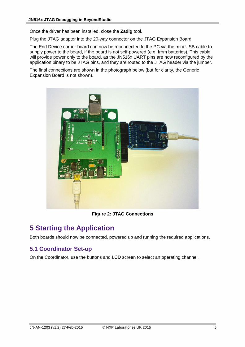
The End Device carrier board can now be reconnected to the PC via the mini-USB cable to supply power to the board, if the board is not self-powered (e.g. from batteries). This cable will provide power only to the board, as the JN516x UART pins are now reconfigured by the application binary to be JTAG pins, and they are routed to the JTAG header via the jumper.
The final connections are shown in the photograph below (but for clarity, the Generic Expansion Board is not shown).
Figure 2: JTAG Connections
5 Starting the Application Both boards should now be connected, powered up and running the required applications.
5.1 Coordinator Set-up On the Coordinator, use the buttons and LCD screen to select an operating channel.
JN-AN-1203 (v1.2) 27-Feb-2015 © NXP Laboratories UK 2015 5

JN516x JTAG Debugging in BeyondStudio 5.2 End Device Set-up In order to begin debugging, a Debug Configuration must be created for the project in BeyondStudio for NXP. To do this, right-click the project in the Project Explorer pane and follow the menu path Debug As>Debug Configurations, or click the drop-down arrow associated with the Debug button on the toolbar and select Debug Configurations. The following dialogue box will now appear.
Select NXP JN51xx Application and then click the New button at the top of the pane.
The above Debug Configurations dialogue box will now automatically update to the layout shown below.
6 © NXP Laboratories UK 2015 JN-AN-1203 (v1.2) 27-Feb-2015

JN516x JTAG Debugging in BeyondStudio
In the Name field of this dialogue box, a name for the Debug Configuration is automatically generated from the target name. This can be changed, if desired.
The application to debug must next be selected in the C/C++ Application field. This is the ELF file, not the binary file, and will end in “_hwdbg.elf”. Use the Search Project button to select the file AN1180_154_HomeSensorEndD_JN5168_hwdbg.elf. Optionally, the Debug Configuration can be set up to automatically build the project before debugging.
JN-AN-1203 (v1.2) 27-Feb-2015 © NXP Laboratories UK 2015 7

JN516x JTAG Debugging in BeyondStudio On the Target tab of the dialogue box (shown below), most users should leave the Use JTAG proxy option selected. No additional parameters are necessary.
8 © NXP Laboratories UK 2015 JN-AN-1203 (v1.2) 27-Feb-2015

JN516x JTAG Debugging in BeyondStudio
On the Debugger tab of the dialogue box (shown below), the default options should be used. These options will load the application binary into the target device and set the program counter to the function named AppColdStart(), ready to run as if the device has been reset.
Once this configuration is complete, the Debug button in the dialogue box can be used to immediately start a debug session, if required.
JN-AN-1203 (v1.2) 27-Feb-2015 © NXP Laboratories UK 2015 9

JN516x JTAG Debugging in BeyondStudio
6 Debugging If the debugging session has not already been started, click on the Debug button on the toolbar or use the keyboard shortcut F11 to start it. BeyondStudio for NXP will start a process in the background called “jp3.exe” to communicate with the JTAG device. It will then start GDB and perform the steps defined in the Debug Configuration. Normally this will be to load the application binary, reset the device and set the program counter to AppColdStart(). BeyondStudio will open the Debug perspective, which should show the processor stalled at AppColdStart(). The program location is indicated by the arrow in the margin and the line is highlighted in green.
• The Debug pane displays the processor stack and allows selection of any stack frame. This will update the other displays to the selected frame.
• The Variables tab shows local variables within the selected stack frame.
• The Breakpoints tab shows all currently configured breakpoints.
• The Registers tab displays the contents of the CPU registers.
• The main display shows the C source code at the location where the CPU is stopped.
• The Disassembly tab shows the assembly language at the location where CPU is stopped.
Processor Stack Source (Current Line Highlighted) Disassembly
10 © NXP Laboratories UK 2015 JN-AN-1203 (v1.2) 27-Feb-2015

JN516x JTAG Debugging in BeyondStudio
6.1 Single Stepping the CPU With the CPU stopped at AppColdStart(), the CPU can be stepped a single line of C source by clicking the Step Over button on the toolbar.
1. Click the Step Over button once to enter the function, then again to step over the call to vAHI_WatchdogStop().
2. The next line is a call to vInitSystem(). Step into this function by clicking the Step Into button on the toolbar.
The updated stack with the additional function is shown in the Debug pane.
6.2 Free Running the CPU To start the CPU executing, click the Resume button on the toolbar. To suspend execution, click the Suspend button on the toolbar.
When the processor is paused, it should be stopped in vAHI_CpuDoze(). This function puts the CPU into doze mode and awaits interrupts to wake it. This application is for an End Device and spends the vast majority of its time with the CPU dozing. Therefore when the CPU is paused, there is a very high chance of it being within this function.
JN-AN-1203 (v1.2) 27-Feb-2015 © NXP Laboratories UK 2015 11

JN516x JTAG Debugging in BeyondStudio 6.3 Resetting the CPU If the CPU is stepped at this point, it is likely that the next line is never reached. This is a symptom of debugging a CPU with many peripherals that continue to run, even while the CPU is stalled.
For example, the Timer peripheral keeps running even when the CPU is stalled from the previous step. The Timer is set up to interrupt on matching a value but, because the Timer kept running while the CPU was stalled, it is now beyond the match value. This means that the interrupt will now not occur until the Timer wraps, which will take a very long time. As a result, the CPU will appear to remain dozing indefinitely. At this point, the best course of action is to reset the CPU and restart from ‘cold start’ conditions. This will also be the case when debugging a device that is a member of a network as while its CPU is stalled, the network will perceive the device to have left. Resuming the CPU could have consequences such as frames being parsed and responded to late, and confusing the state of the network. It may be that in this case, again, the best thing to do is to restart and rejoin the network.
To restart the device, click the Restart button on the toolbar. The CPU is reset and BeyondStudio once again shows the CPU stalled at the AppColdStart() function.
6.4 Setting Breakpoints Breakpoints may be used to stop CPU execution at any program counter address.
Locate the function vProcessRead() within the file AN1180_154_HomeSensorEndD.c.
To set a breakpoint, locate the line within the source code (or Disassembly tab) and double-click in the margin. A blue circle in the margin indicates the presence of a breakpoint. The breakpoint is also listed in the Breakpoints tab of the BeyondStudio interface.
12 © NXP Laboratories UK 2015 JN-AN-1203 (v1.2) 27-Feb-2015

JN516x JTAG Debugging in BeyondStudio
Note that JN516x devices support only 4 breakpoints. Attempts to set further breakpoints will succeed but will not be acted upon by the CPU. Features such as “Run to cursor” and “Step out” make use of a breakpoint; therefore, the user must ensure that only 3 breakpoints are in use at any one time by selectively disabling or removing breakpoints in the Breakpoints tab.
Free-run the CPU by clicking the Resume button on the toolbar. The application will now run through the initialisation sequence and associate with the Coordinator. When the Coordinator sends a frame to the End Device, this will be processed and execution should halt on the breakpoint.
6.5 Examining the Processor Stack The processor stack maintains the context of execution across function calls. Most functions that are called create a new frame on the stack in which to save the previous context and store local variables. This Application Note is simple and does not have many nested function calls. This means that it does not have a very deep stack to examine; the deepest level attained is 4 entries, at the ProcessRead() function.
The stack frame may now be examined. In this function there are two local variables. These are shown in the Variables tab.
JN-AN-1203 (v1.2) 27-Feb-2015 © NXP Laboratories UK 2015 13

JN516x JTAG Debugging in BeyondStudio
The previous frames on the stack may be selected in the Debug window. The Variables tab will be updated with the local variables within the selected stack frame.
6.6 Viewing Global Variables Global variables may be viewed in the Expressions pane of the BeyondStudio interface. To view a global variable (for example, the main application state structure sDemoData), locate a reference to it in the main view. Right-click on the variable name and select Add Watch Expression from the context menu (see screenshot below). The expression is added to the Expressions pane. The structure may be expanded and its contents viewed from this pane.
6.7 Finishing a Debug Session When a debug session is no longer required, it must be terminated by clicking the Terminate button on the toolbar. This will kill the GDB and jp3 processes used to control
14 © NXP Laboratories UK 2015 JN-AN-1203 (v1.2) 27-Feb-2015

JN516x JTAG Debugging in BeyondStudio
the JN516x device, but will not exit the Debug perspective. To change back to the normal
C/C++ perspective, click on the C/C++ button on the toolbar.
6.8 Catching Exceptions When an exception occurs in the CPU, the debugger halts the CPU and allows the user to examine the state of the program at the point where the exception occurred.
As an example, add the following code to the function AppColdStart(), which can be found in AN1180_154_HomeSensorEndD.c. /* General initialisation: reset hardware */ vInitSystem(); // Generate an alignment exception. *(uint32*)(0x400001) = 0;
Rebuild the End Device application using the Build button on the toolbar. The application should build.
Begin a new debug session by clicking the Debug button on the toolbar. The newly compiled application will be loaded into the target JN516x device and execution paused at AppColdStart(). The application may now be set free-running by clicking the Resume button on the toolbar. The CPU will execute the code resulting in an alignment exception which will suspend execution. The Debug tab shows that the CPU is suspended with an alignment exception.
JN-AN-1203 (v1.2) 27-Feb-2015 © NXP Laboratories UK 2015 15

JN516x JTAG Debugging in BeyondStudio
The line that caused the exception is highlighted above in the main window.
6.9 Using the Watchdog Timer The Watchdog Timer is started by default on the JN516x device. When the bootloader detects a debug-enabled binary, it stops the Watchdog Timer. This means that to make use of the Watchdog Timer when debugging using JTAG, the timer must be re-enabled by calling the vAHI_WatchdogStart() function. The default behaviour of the Watchdog Timer is to reset the device. When running with the debugger, this will cause the JTAG hardware to be reset and the debugger to lose its connection. Therefore, when using the Watchdog Timer, the exception must always be enabled.
As an example, add the following code to the function AppColdStart(), which can be found in AN1180_154_HomeSensorEndD.c. /* General initialisation: reset hardware */ vInitSystem(); /* Initialise watchdog timer */ vAHI_WatchdogStart(12); vAHI_WatchdogException(TRUE); /* Cause watchdog timeout */ while(1); Rebuild the End Device application using the Build button on the toolbar. The application should build.
Begin a new debug session by clicking the Debug button on the toolbar. The newly compiled application will be loaded into the target JN516x device and execution paused at AppColdStart(). The application may now be set free-running by clicking the Resume button on the toolbar. The CPU will execute the code. After around 17 seconds, a watchdog exception will occur which will suspend execution. The Debug tab shows that the CPU is suspended with a watchdog exception.
16 © NXP Laboratories UK 2015 JN-AN-1203 (v1.2) 27-Feb-2015

JN516x JTAG Debugging in BeyondStudio
6.10 Device Reset The JN516x Integrated Peripherals API function vAHI_SwReset() may be used by an application to cause a device reset. Actually resetting the device would reset the JTAG hardware and cause the debugger to loose communication with the device. Therefore the debugger catches this condition to allow the user to reset the debug session.
As an example, add the following code to the function AppColdStart(), which can be found in AN1180_154_HomeSensorEndD.c. /* General initialisation: reset hardware */ vInitSystem(); /* Cause device reset */ vAHI_SwReset();
Rebuild the End Device application using the Build button on the toolbar. The application should build.
Begin a new debug session by clicking the Debug button on the toolbar. The newly compiled application will be loaded into the target JN516x device and execution paused at AppColdStart(). The application may now be set free-running by clicking the Resume button on the toolbar. The CPU will execute the code resulting in a reset exception which will suspend execution. The Debug tab shows that the CPU is suspended with a reset exception.
JN-AN-1203 (v1.2) 27-Feb-2015 © NXP Laboratories UK 2015 17

JN516x JTAG Debugging in BeyondStudio
The reset exception is raised by executing a syscall instruction in the CPU. This is done with the JN516x Integrated Peripherals API library, for which source code is not available for the main window.
Allowing the program to continue after this exception occurs will result in a communication loss with the device.
If working with an application that issues software resets during normal operation, it may be useful to automatically restart from a reset exception. This can be done by adding the following GDB commands to a file and saving it in the root of the current project: hbreak vMicroSyscall if $R3==0 commands silent sreset set $pc=AppColdStart continue end The command file should be run at the beginning of each debug session by adding a source command to the ‘Run commands’ section of the debug configuration: source <filename>
18 © NXP Laboratories UK 2015 JN-AN-1203 (v1.2) 27-Feb-2015

JN516x JTAG Debugging in BeyondStudio
7 Using Debug Printf The debug Printf library may be used to print values to the GDB console while minimising the time for which the CPU is stalled. As an example, add the following code to AppColdStart(), which can be found in AN1180_154_HomeSensorEndD.c. /* General initialisation: reset hardware */ vInitSystem(); #if defined HWDEBUG DBG_vJtagInit(); #else DBG_vUartInit(DBG_UART, DBG_BAUD_RATE); #endif /* HWDEBUG */ DBG_vPrintf(TRUE, "Hello world!\n");
Add the following include directives at the start of the file: #include "dbg_jtag.h" #include "dbg_uart.h"
The following changes must also be made to the End Device Makefile:
• Enable the DBG library in the C preprocessor
• Add the DBG library to the project’s include paths
• Add the DBG library to the list of linked libraries
The lines in the Makefile are as follows: CFLAGS += -DDBG_ENABLE INCFLAGS += -I$(COMPONENTS_BASE_DIR)/DBG/Include APPLIBS += DBG
Recompile the End Device application using the Build button on the toolbar. The application should build.
Begin a new debug session by clicking the Debug button on the toolbar. The newly compiled application will be loaded into the target JN516x device and execution paused at AppColdStart(). The application may now be set free-running by clicking the Resume button on the toolbar. The following output should be observed in the Console tab:
JN-AN-1203 (v1.2) 27-Feb-2015 © NXP Laboratories UK 2015 19

JN516x JTAG Debugging in BeyondStudio
8 Additional Information
8.1 Sleeping End Devices In this release of BeyondStudio for NXP, the debugging of sleeping End Devices via JTAG is not supported. When a JN516x device enters sleep mode, the debug unit within the CPU is powered down. This means that the JTAG hardware loses its connection with the CPU and the debug session is terminated.
8.2 Compile Time Optimisation When compiling for debug, the toolchain disables optimisations and link-time optimisation, because these optimisations interfere with the generation of debug information and lead to a sub-optimal debugging experience. This has the side effect that the output binary will grow in size significantly as the compiler cannot make space saving optimisations. Compiler optimisations can be enabled by changing the DEBUG variable in the application Makefile as follows: # Debug options define DEBUG for HW debug DEBUG ?= HW_SIZEOPT Note that the optimisations that the compiler now performs may lead to the execution order of the program being different from the source code – for example, functions may be inlined.
8.3 Link-Time Optimization Link-time optimisation is not recommended to be used when debugging, because the aggressive optimisations that it applies makes the debugger difficult to use. If the binary size means that these optimisations are really necessary then link-time optimisation (LTO) can be enabled by setting the DISABLE_LTO variable to 0 in the application Makefile: DISABLE_LTO = 0
20 © NXP Laboratories UK 2015 JN-AN-1203 (v1.2) 27-Feb-2015

JN516x JTAG Debugging in BeyondStudio
9 DR1222 (JTAG Expansion Board) Schematic
JN-AN-1203 (v1.2) 27-Feb-2015 © NXP Laboratories UK 2015 21

JN516x JTAG Debugging in BeyondStudio
Revision History Version Notes
1.0 First release 1.1 Updated branding 1.2 Added schematic for DR1222 JTAG Expansion Board
Important Notice Limited warranty and liability — Information in this document is believed to be accurate and reliable. However, NXP Semiconductors does not give any representations or warranties, expressed or implied, as to the accuracy or completeness of such information and shall have no liability for the consequences of use of such information. NXP Semiconductors takes no responsibility for the content in this document if provided by an information source outside of NXP Semiconductors.
In no event shall NXP Semiconductors be liable for any indirect, incidental, punitive, special or consequential damages (including - without limitation - lost profits, lost savings, business interruption, costs related to the removal or replacement of any products or rework charges) whether or not such damages are based on tort (including negligence), warranty, breach of contract or any other legal theory.
Notwithstanding any damages that customer might incur for any reason whatsoever, NXP Semiconductors’ aggregate and cumulative liability towards customer for the products described herein shall be limited in accordance with the Terms and conditions of commercial sale of NXP Semiconductors.
Right to make changes — NXP Semiconductors reserves the right to make changes to information published in this document, including without limitation specifications and product descriptions, at any time and without notice. This document supersedes and replaces all information supplied prior to the publication hereof.
Suitability for use — NXP Semiconductors products are not designed, authorized or warranted to be suitable for use in life support, life-critical or safety-critical systems or equipment, nor in applications where failure or malfunction of an NXP Semiconductors product can reasonably be expected to result in personal injury, death or severe property or environmental damage. NXP Semiconductors and its suppliers accept no liability for inclusion and/or use of NXP Semiconductors products in such equipment or applications and therefore such inclusion and/or use is at the customer’s own risk.
Applications — Applications that are described herein for any of these products are for illustrative purposes only. NXP Semiconductors makes no representation or warranty that such applications will be suitable for the specified use without further testing or modification.
Customers are responsible for the design and operation of their applications and products using NXP Semiconductors products, and NXP Semiconductors accepts no liability for any assistance with applications or customer product design. It is customer’s sole responsibility to determine whether the NXP Semiconductors product is suitable and fit for the customer’s applications and products planned, as well as for the planned application and use of customer’s third party customer(s). Customers should provide appropriate design and operating safeguards to minimize the risks associated with their applications and products.
NXP Semiconductors does not accept any liability related to any default, damage, costs or problem which is based on any weakness or default in the customer’s applications or products, or the application or use by customer’s third party customer(s). Customer is responsible for doing all necessary testing for the customer’s applications and products using NXP Semiconductors products in order to avoid a default of the applications and the products or of the application or use by customer’s third party customer(s). NXP does not accept any liability in this respect.
Export control — This document as well as the item(s) described herein may be subject to export control regulations. Export might require a prior authorization from competent authorities.
All trademarks are the property of their respective owners.
NXP Semiconductors
For the contact details of your local NXP office or distributor, refer to:
www.nxp.com
22 © NXP Laboratories UK 2015 JN-AN-1203 (v1.2) 27-Feb-2015