jean-marie bussat – january 31, 20021 fppa2000 characterization history sumary of tests done at...
TRANSCRIPT

Jean-Marie Bussat – January 31, 20021
FPPA2000 characterization history Sumary of tests done at LBNL
FPPA2000 characterization history Sumary of tests done at LBNL

Jean-Marie Bussat – January 31, 20022
First measurementsFirst measurements
Preamplifier test output
Pulse input
OzTek socket+ Ceramic FPPAFPPA digital
outputs
Power supplies and temperature inputs
Leakage current input
FPPA output
FPPA mode Selection (gains)
Clock inputs
First measurements on ceramic packages started April 2001
Three problems found :Gains are wrongPreamplifier response has an
undershootNoise level is too high (40ke-)

Jean-Marie Bussat – January 31, 20023
Wrong gainsWrong gains
Gains don’t have the right value: 1, 3.7, 6.4, 21 instead of 1, 5, 9, 33 Design issue: software doesn’t take care of metal resistance
PreamplifierPreamplifier
Amp.Amp. Amp.Amp.
Amp.Amp. Amp.Amp.
1.3mm
0.9mm
R’sR’sR2
R150
External decouplingCapacitor (100nF)
Parasitic resistance~25-30
Rp
Gain = 1 + R2
R1 + Rp
Small less noise

Jean-Marie Bussat – January 31, 20024
Undershoot in PA responseUndershoot in PA response
Preamp.
Cf
Rf
Cf = 22pF (design value)
Cf = 34pF

Jean-Marie Bussat – January 31, 20025
Excessive noiseExcessive noise
0.00E+00
5.00E+03
1.00E+04
1.50E+04
2.00E+04
2.50E+04
3.00E+04
3.50E+04
4.00E+04
4.50E+04
5.00E+04
0.00E+00 5.00E-11 1.00E-10 1.50E-10 2.00E-10 2.50E-10 3.00E-10 3.50E-10
Detector Capacitance [F]
Pre
am
p. N
ois
e [
Ke
-]
Measured
Simulated
Meas. Noise = 14.5Ke- + 100e-/pF
Sim. Noise = 8.3Ke- + 20e-/pF
"Real" noise: gaussian distribution
Std. Plastic Part: Chip 2599x25 Amplifier=3.7 mV0.4 pC = 270 mV Noise = 34 ke

Jean-Marie Bussat – January 31, 20026
Noise investigation (1)Noise investigation (1)
Noise investigation started in May 2001.
First hypothesis : process problem* Wrong size of input transistor ?
No (checked under microscope)* Intrinsic base resistor of input transistor too high ? No (measurement of same transistor on the Process Control Monitor gives result within specs).
Second hypothesis : preamplifier not guilty, noise coming from elsewhere ?* A minimalist test setup dedicated to the preamplifier alone is built (digital part not powered, no clocks)
Two attempts of re-bonding- PLCC68- Chip on board

Jean-Marie Bussat – January 31, 20027
Noise investigation (2)external sources of noise
Noise investigation (2)external sources of noise
• Noise=pickup noise ?
• Noise=received “noise” ?
Noise “waveform” asynchronous to 40MHz clock.
Noise still there without clock.No
A little : ~100-200MHz signal
Need a Faraday cage
Found an aluminum box that works well
Noise still there Comes from inside FPPA…

Jean-Marie Bussat – January 31, 20028
Noise investigation (3)1st preamplifier-only test
Noise investigation (3)1st preamplifier-only test
top bottom
Tried with a PLCC68 package(cavity needs to be large because chip size is 4mm x 5mm)
External components placed as close as possible to the chip
4cm
4cm
L
Package lid length: PLCC68: L ~ 1cm avg.TQFP52: L ~ 1mm (final package)
Pulse shape ok with Cf = 22 pF ~ 10pF parasitics !!
Need to repackage without adding parasitic capacitance Chip on board
Too much parasitic capacitance makes preamplifier unstable

Jean-Marie Bussat – January 31, 20029
Noise investigation (4)2nd preamplifier-only test
Noise investigation (4)2nd preamplifier-only test
top bottom
Use chip-on-board direct bonding to minimize parasitic capacitances
Components placed as close as possible to the chip
No more oscillations Same noise level as with complete test board
* Noise is not coming from the FPU: Preamplifier problem ???* There’s no correlation between the noise observed on the sensitive points of the preamplifier (bias decoupling points) and the noise at the output.* It’s impossible to insure that the bias is not responsible with this setup.
Need to physically isolate the preamplifier from the FPU "Chip surgery": FIB (Focused Ion Beam)

Jean-Marie Bussat – January 31, 200210
Noise investigation (5)Noise investigation (5)
FIB first iteration: June 2001.
* Design of a dedicated chip on board PCB* 5 chips bonded, 4 tested OK, 3 sent for FIB (preamplifier alone, no internal bias)
Noise level down to ~ 20ke-
* Simulation with parasitic resistances shows an increase of noise level from 10ke- to 17ke- . Measured values are close but not enough.
y = 103x + 14523
y = 16x + 8367
y = 70x + 8197
0
5000
10000
15000
20000
25000
30000
35000
40000
45000
50000
0 50 100 150 200 250 300 350
CDetector [pF]
Noi
se [
e-]
Measured Ceramic Simulated (No parasitic resistance) FIB-Card 4 FIB-Card 5
Ceramic
FIB
Schematicsimulation(ideal circuit)

Jean-Marie Bussat – January 31, 200211
Noise investigation (6)Environmental problems
Noise investigation (6)Environmental problems
Noise is studied using a spectrum analyzer instead of an oscilloscope. Noise spectrum contains a lot of pickup noise (90-200MHz). Noise is coupled via power supply lines
000E+0
20E-6
40E-6
60E-6
80E-6
100E-6
120E-6
000E+0 50E+6 100E+6 150E+6 200E+6
Frequency [Hz]
Am
plit
ude
[V]
Box closedAnalyser noise floor Test board powered using
batteries.
Noise level down to 15-17ke- :
Matches simulation results

Jean-Marie Bussat – January 31, 200212
Noise investigation (7)Noise investigation (7)
Noise cause investigation: July 2001.
* Previous results don’t ensure that there’s no contribution from the FPU.
* The preamplifier needs a bias voltage and a bias current
Simulations show that the current input is more sensitive than the voltage input
Assuming that an external bias current is the solution (like in the 1998 prototype
of the FPPA that had the same noise level than in simulation), nothing proves that
the contribution of the voltage input is negligible.
FIB second iteration
* Standard ceramic packaged FPPA with a cut on the preamplifier bias current input
only
* 3 chips processed, 1 chip destroyed during transport.

Jean-Marie Bussat – January 31, 200213
Noise investigation (8)second FIB results
Noise investigation (8)second FIB results
~FIB-noise2\D007~FIB-noise2\D006
4V pulse Injected40 dB attenuationCINJ = 8 pF
x25 Amplifier=2.0 mV 0.32 pC = 255 mV Noise = 15.7 ke
Battery poweredtest board
Noise understoodNo contribution from reference voltage

Jean-Marie Bussat – January 31, 200214
Pulse shape study (1)Pulse shape study (1)
Pulse shape study: July/August to October 2001.
Fact: The pulse shape at the preamplifier output is affected by the setting of the FPU multiplexer.
* Multiplexer set to any slow control channel preamplifier pulse is normal.
* Multiplexer set to any signal channel (gain 1, 5, 9 or 33) preamplifier pulse is distorted.
Effect is the same for all chips (plastic or ceramic package). Distortion is directly proportional to the value of the selected gain.
indicates a coupling through the input of the preamplifier. Distortion looks like the derivation of the input pulse.
indicates a capacitive coupling.
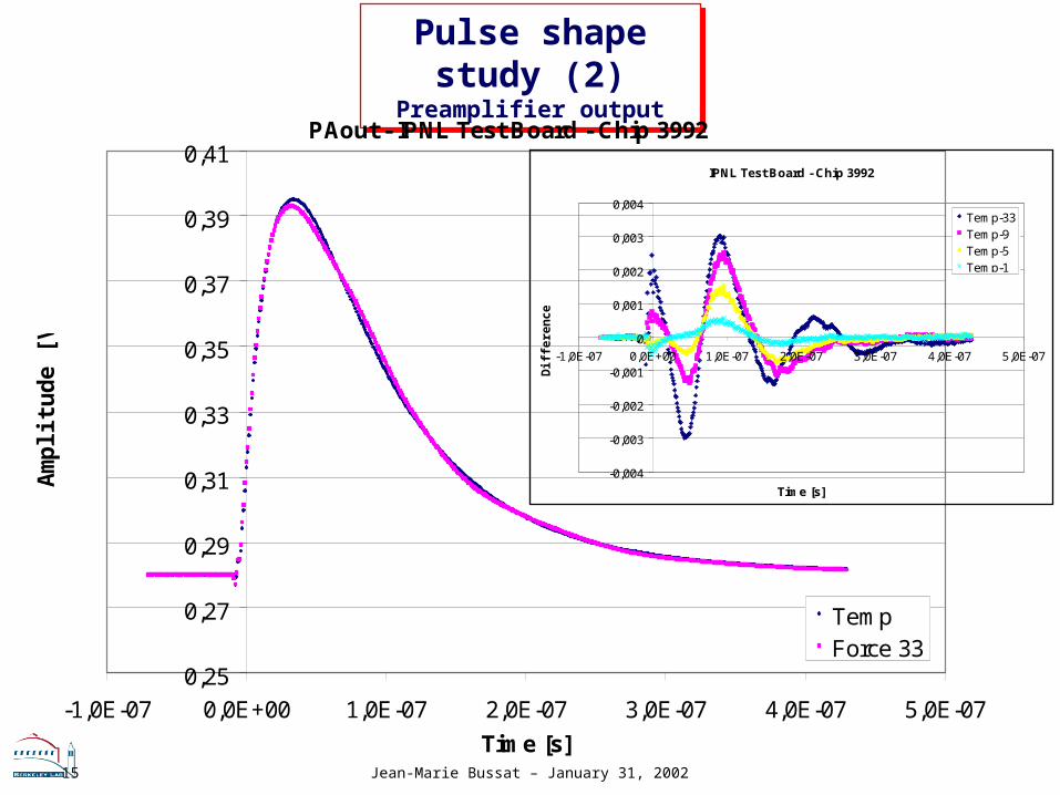
Jean-Marie Bussat – January 31, 200215
Pulse shape study (2)Preamplifier output
Pulse shape study (2)Preamplifier output
PAout - IPNL Test Board - Chip 3992
0,25
0,27
0,29
0,31
0,33
0,35
0,37
0,39
0,41
-1,0E-07 0,0E+00 1,0E-07 2,0E-07 3,0E-07 4,0E-07 5,0E-07
Time [s]
Am
pli
tud
e [V
]
TempForce 33
IPNL Test Board - Chip 3992
-0,004
-0,003
-0,002
-0,001
0
0,001
0,002
0,003
0,004
-1,0E-07 0,0E+00 1,0E-07 2,0E-07 3,0E-07 4,0E-07 5,0E-07
Time [s]
Dif
fere
nce
[V
]
Temp-33Temp-9Temp-5Temp-1

Jean-Marie Bussat – January 31, 200216
Pulse shape study (3)Pulse shape study (3)
The effect has never been seen on soldered chips.- Any distortion that is visible at the output of the preamplifier is
also visible at the output of the FPPA If the output of the FPPA is “clean”, the output of the preamplifier is also “clean”.
- True for M0’ as well as for Proto99 and Proto99++ where no effects were observed.
- Even if Proto99 and Proto99++ were using the 98’ prototype of the FPPA, some chips showed this behavior during testing (on socket). The effect was so rare that it was at that time associated to malfunctioning chips.

Jean-Marie Bussat – January 31, 200217
Pulse on M0'Pulse on M0'
Sample number (25ns/sample)
AD
C c
ount
Run 11144Max. intensity in xtal 2 (FPPA #2697)5ns delay on ADC clock
Normal pulse shape, pulse timing as simulated
Pulse reconstructed from ADC data obtained with unsynchronized acquisition

Jean-Marie Bussat – January 31, 200218
Pulse shape (4)Pulse shape (4)
Pulse shape study (October 2001) :
The effect remain unchanged whatever the output buffer load is.
The preamplifier pulse is not affected by any signal applied on the slow control inputs
Pulse distortion doesn’t come from the output of the FPPA.
The effect exist if the FPU clock is running or if the FPU is forced in sample mode.
The distortion disappear if the FPU is forced in hold mode.
????
The effect is four time smaller on FIB’d chip with external preamplifier bias.
The bias current input of the preamplifier is a coupling path.
But this is not the only one.
Pulse distortion is also visible on the IPNL test board.
The effect doesn’t come from the layout of the test board.
During three days, it was impossible to reproduce the effect whatever was done to the chip or the board.
The problem is probably coming from the contacts that are not perfects in the case of the use of a socket.

Jean-Marie Bussat – January 31, 200219
Pulse shape (5)Internal/External bias current
Pulse shape (5)Internal/External bias current
Chip 2599 (Plastic)
-0,1
0
0,1
0,2
0,3
0,4
0,5
0,6
0,7
0,0E+00 5,0E-08 1,0E-07 1,5E-07 2,0E-07 2,5E-07 3,0E-07 3,5E-07 4,0E-07 4,5E-07
Time [s]
Am
plitu
e [V
]
Force 1Force 5Force 9Force 33Force Ref ADC
Chip 18 (FIB'd)
-0,1
0
0,1
0,2
0,3
0,4
0,5
0,6
0,7
0,0E+00 5,0E-08 1,0E-07 1,5E-07 2,0E-07 2,5E-07 3,0E-07 3,5E-07 4,0E-07 4,5E-07
Time [s]
Am
plitu
e [V
]
Force 1Force 5Force 9Force 33Force Ref ADC
Chip 18 (FIB'd) Deviation from "ideal" (MUX set on ADCRef)
-0,010
-0,005
0,000
0,005
0,010
0,015
0,0E+00 1,0E-07 2,0E-07 3,0E-07 4,0E-07 5,0E-07
Time [s]
Am
pli
tud
e [
V]
Force 1Force 5Force 9Force 33
Chip 2599 (Plastic) Deviation from "ideal" (MUX set on ADCRef)
-0,03
-0,02
-0,01
0
0,01
0,02
0,03
0,04
0,0E+00 5,0E-08 1,0E-07 1,5E-07 2,0E-07 2,5E-07 3,0E-07 3,5E-07 4,0E-07 4,5E-07
Time [s]
Am
plit
ud
e [
V]
Force 1Force 5Force 9Force 33
Internal biascurrent
External biascurrent

Jean-Marie Bussat – January 31, 200220
OscillationsOscillations
Oscillations study: October 2001.
Fact: Some oscillations have been observed at the output of the preamplifier during the test
of 1500 FPPA's in Lyon.
Chips that were oscillating on the test bench in Lyon are not oscillating on the test
board used at LBNL (quasi-identical layout).
The test board used in Lyon has been brought to LBNL.
No oscillations can be seen…
Environmental problem
The preamplifier is sensitive to the load that is connected to its output.
It is possible, in some marginal cases, to induce an oscillation by changing the way
the buffer that is used to look at the output of the preamplifier is connected.
Again, the difficulties encountered to reproduce the problem suggest that it could be related to a contact problem (No oscillations observed on the M0’
modules).
Jean-Marie Bussat – January 31, 200221
TimingTiming
Timing study: October 2001.
Facts: * There’s some problems on the preamplifier that prevent a fine analysis of the FPU
(noise and linearity measurements are dominated by the preamplifier characteristics).
* Some timing problems have been observed at CERN on M0’
Timing is defined by the FPU but it is difficult to study it through the preamplifier.
FIB third iteration
- Ceramic FPPA (the only type that can be modified with FIB).
- The preamplifier is disconnected. Its output becomes the input of the FPPA.
This way it is possible to input any given signal to the FPU to
check its response.
- Two fully working chips sent for modification.
Both are dead after FIB : same behavior, short circuit on VCC and dead
bias generator.
Too sensitive node for FIB
Timing has to be checked on the full FPPA (M0').