japanese patent 1975-127647 by hagiwara at sony …aiplab.com/jp1975-127647.pdfjapanese patent...
TRANSCRIPT
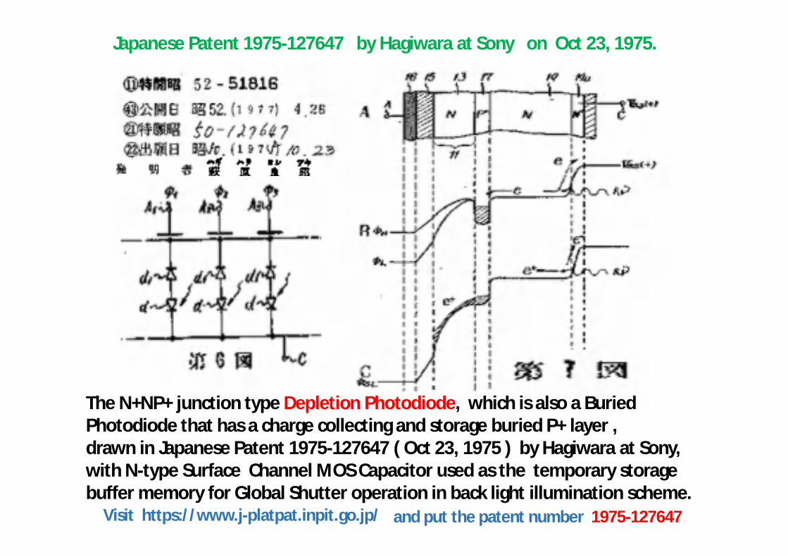
Japanese Patent 1975-127647 by Hagiwara at Sony on Oct 23, 1975.
The N+NP+ junction type Depletion Photodiode, which is also a Buried Photodiode that has a charge collecting and storage buried P+ layer ,drawn in Japanese Patent 1975-127647 ( Oct 23, 1975 ) by Hagiwara at Sony, with N-type Surface Channel MOS Capacitor used as the temporary storage buffer memory for Global Shutter operation in back light illumination scheme.
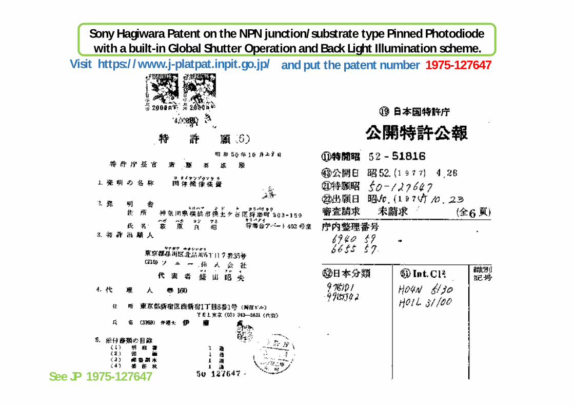
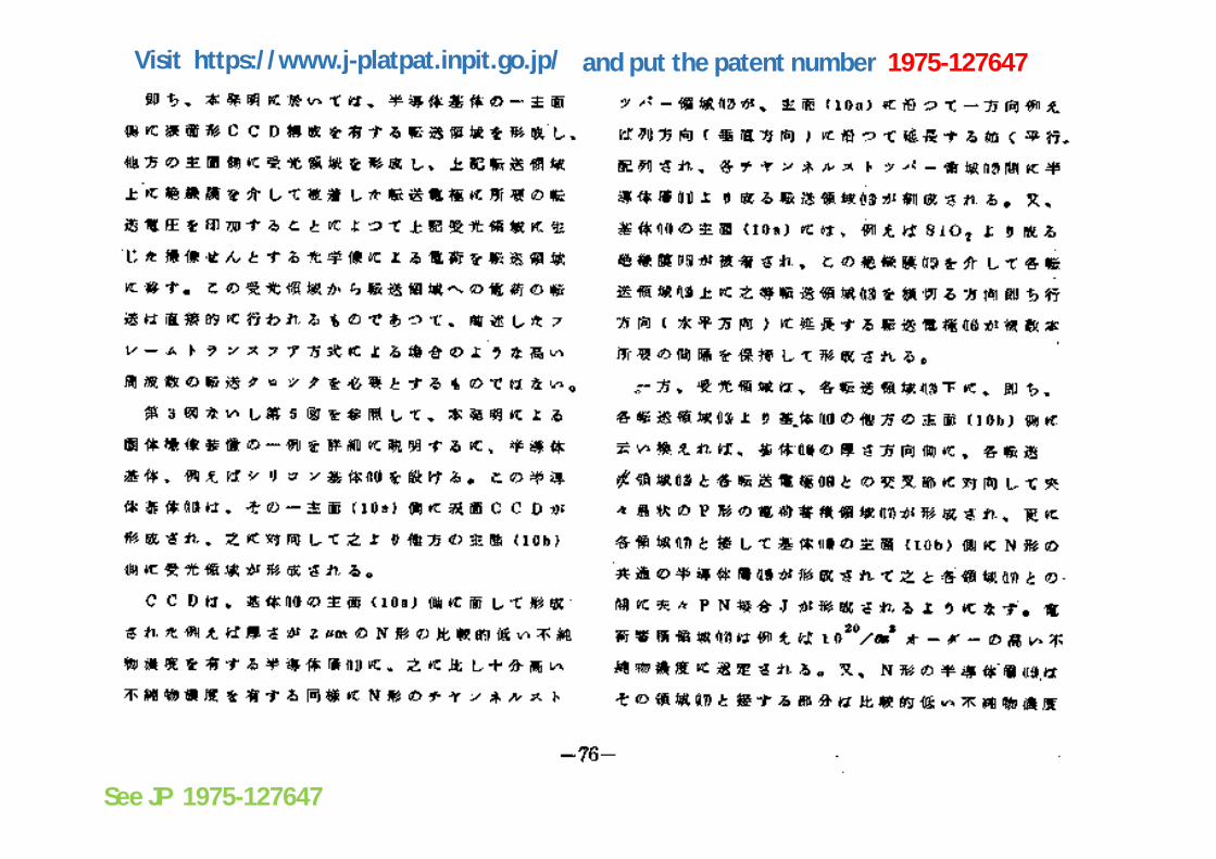
Visit https://www.j-platpat.inpit.go.jp/ and put the patent number 1975-127647

Buried Photodiode was invented by Hagiwara at Sony in 1975
Front Light
VCTG
CTDe+ e+
This is also a Pinned Photodiode.
VCTG
CTG
PN
SiO2
SiO2N+
e+e+N e+ e+ CTD
Back Light
BuriedP-LayerPinned
Photodiode
+Vsub
+Vsub
BackLight
Pinned
Clocking ① Clocking ②
NPN junction type Pinned Photodiodewith the built-in Global Shutter functionwith the MOS capacitor Buffer Memory
Capacitance which can store temporally the signal photo charge (e+) by clocking ① .
Clocking②
Clocking①
Clocking Mode ① for Global Shutter Operation Mode with MOS Buffer Memory Capacitor .
Clocking Mode ②for Charge Transferto the adjacent CTD
Fig. 7
Visit https://www.j-platpat.inpit.go.jp/ and put the patent number 1975-127647

e+
Clocking ① forGlobal Shutter Operation Mode with the MOS Buffer Memory Capacitance whichcan store temporally the signal photo charge (e+) .
10 μm or moreThe back light can be blocked from reaching the front
silicon wafer surface for Global Shutter Operation Mode.
Fig. 7
Sony Hagiwara Patent on the NPN junction/substrate type Pinned Photodiodewith a built-in Global Shutter Operation and Back Light Illumination scheme.
①
②
Clocking ② forCharge TransferOperation Modeto the adjacent CTD
Front Light
SiO2
P
SiO2
N
N
Sub
Clock
Back Light
e+ e+ e+ e+ CTD
e+ e+ e+ e+
①
②
GSCTG Main Surface
Global ShutterCharge TransferGate working asMOS CapacitorBuffer Memory
See JP 1975-127647
Visit https://www.j-platpat.inpit.go.jp/ and put the patent number 1975-127647
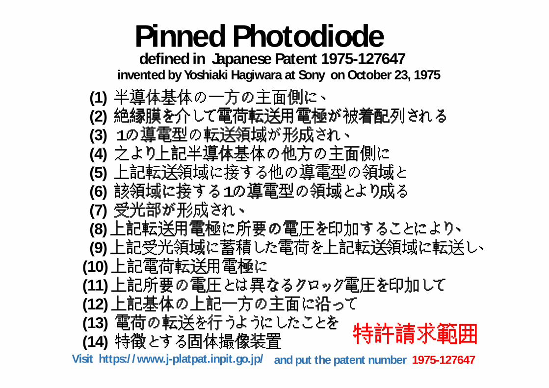
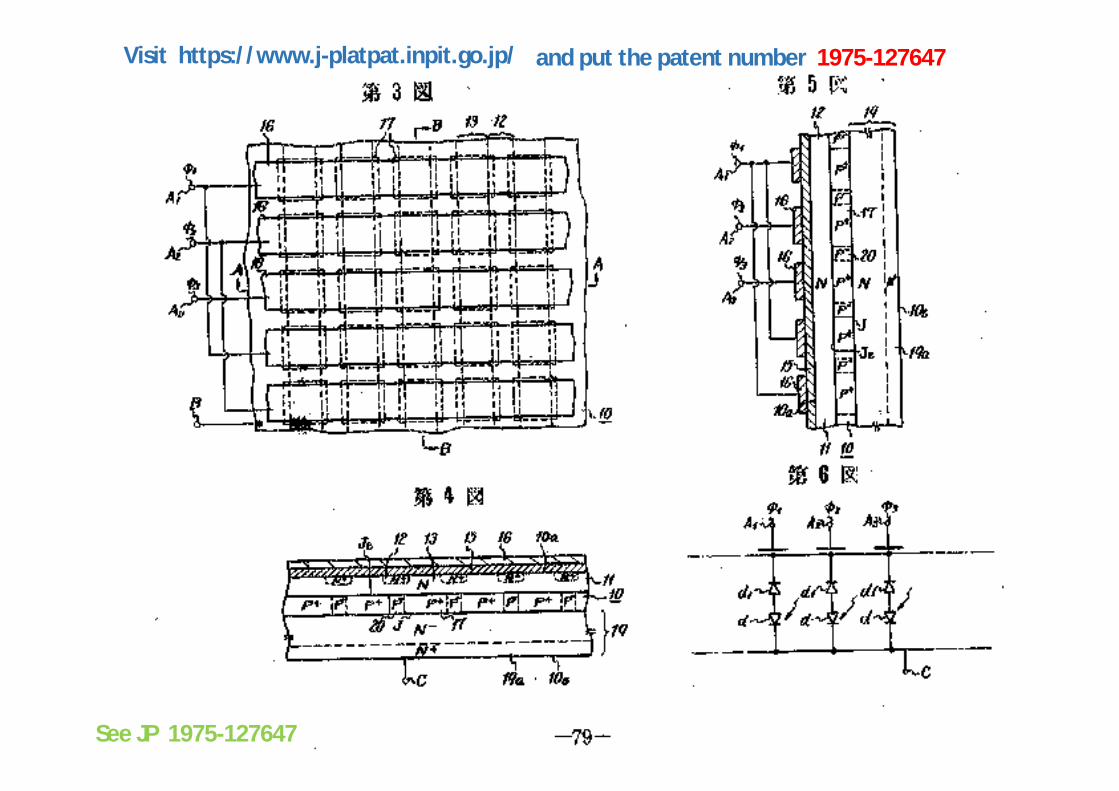
(1) 半導体基体の一方の主面側に、(2) 絶縁膜を介して電荷転送用電極が被着配列される(3) 1の導電型の転送領域が形成され、(4) 之より上記半導体基体の他方の主面側に(5) 上記転送領域に接する他の導電型の領域と(6) 該領域に接する1の導電型の領域とより成る(7) 受光部が形成され、(8) 上記転送用電極に所要の電圧を印加することにより、(9) 上記受光領域に蓄積した電荷を上記転送領域に転送し、
(10) 上記電荷転送用電極に(11)上記所要の電圧とは異なるクロック電圧を印加して(12)上記基体の上記一方の主面に沿って(13) 電荷の転送を行うようにしたことを(14) 特徴とする固体撮像装置
Pinned Photodiode invented by Yoshiaki Hagiwara at Sony on October 23, 1975
defined in Japanese Patent 1975-127647
特許請求範囲Visit https://www.j-platpat.inpit.go.jp/ and put the patent number 1975-127647

(1) Along the main surface of the semiconductor substrate(1) 半導体基体の一方の主面側に、
Main Surface
NPNPsub junction type Pinned Photodiode
The Substrate (Sub) can be N-type, P-type or Intrinsic silicon substrate.
SiO2
Sub
GSCTG
SiO2
See JP 1975-127647
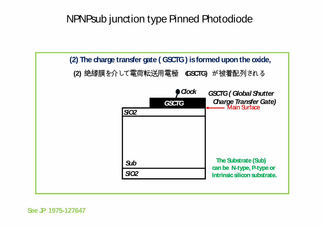
(2) The charge transfer gate ( GSCTG ) is formed upon the oxide,
(2) 絶縁膜を介して電荷転送用電極 (GSCTG) が被着配列される
CTG
The Substrate (Sub) can be N-type, P-type or Intrinsic silicon substrate.
GSCTG
Clock GSCTG ( Global ShutterCharge Transfer Gate)
Main SurfaceMain Surface
The Substrate (Sub) can be N-type, P-type or Intrinsic silicon substrate.
SiO2
Sub
GSCTG
SiO2
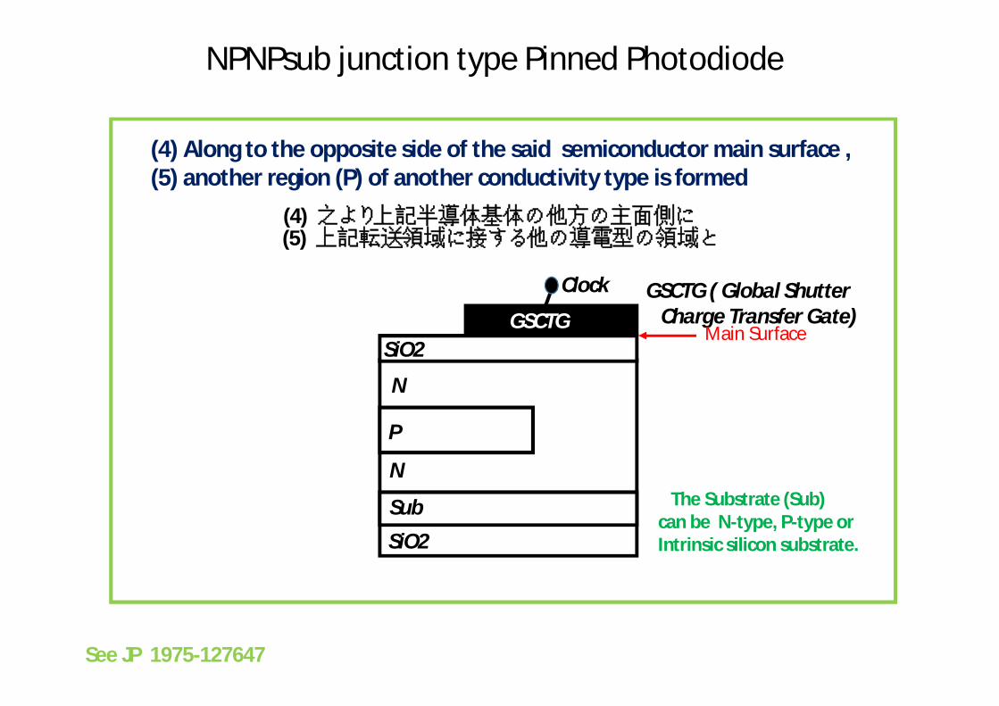
NPNPsub junction type Pinned Photodiode
See JP 1975-127647

(3) 1の導電型の転送領域が形成され、(3) The charge transfer region ( N ) of the first conductivity is formed,
CTG
The Substrate (Sub) can be N-type, P-type or Intrinsic silicon substrate. SiO2
SiO2
N
Sub
GSCTG
Clock GSCTG ( Global ShutterCharge Transfer Gate)
Main Surface
NPNPsub junction type Pinned Photodiode
See JP 1975-127647
CTG
(4) Along to the opposite side of the said semiconductor main surface ,(5) another region (P) of another conductivity type is formed
(4) 之より上記半導体基体の他方の主面側に(5) 上記転送領域に接する他の導電型の領域と
The Substrate (Sub) can be N-type, P-type or Intrinsic silicon substrate. SiO2
P
SiO2
N
N
Sub
GSCTG
Clock GSCTG ( Global ShutterCharge Transfer Gate)
Main Surface
NPNPsub junction type Pinned Photodiode
See JP 1975-127647
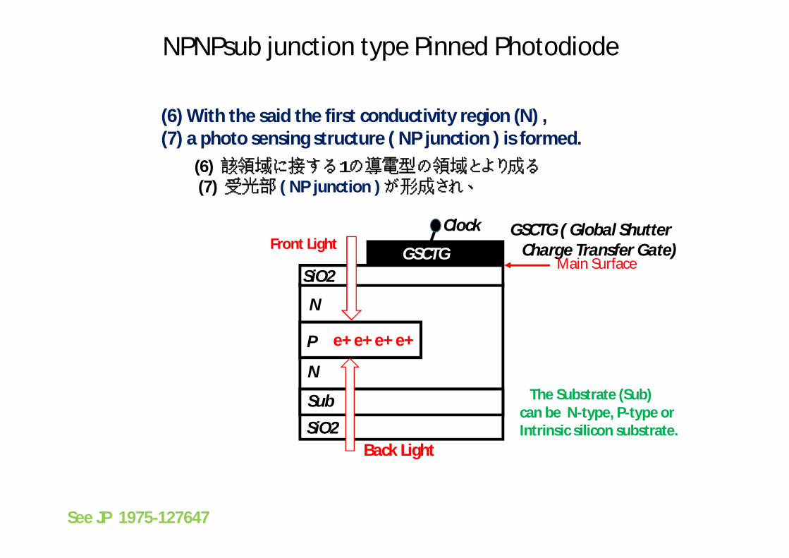
(6) With the said the first conductivity region (N) ,(7) a photo sensing structure ( NP junction ) is formed.
(6) 該領域に接する1の導電型の領域とより成る(7) 受光部 ( NP junction ) が形成され、
The Substrate (Sub) can be N-type, P-type or Intrinsic silicon substrate.
Front Light
SiO2
P
SiO2
N
N
Sub
GSCTG
Clock
Back Light
e+ e+ e+ e+
GSCTG ( Global ShutterCharge Transfer Gate)
Main Surface
NPNPsub junction type Pinned Photodiode
See JP 1975-127647
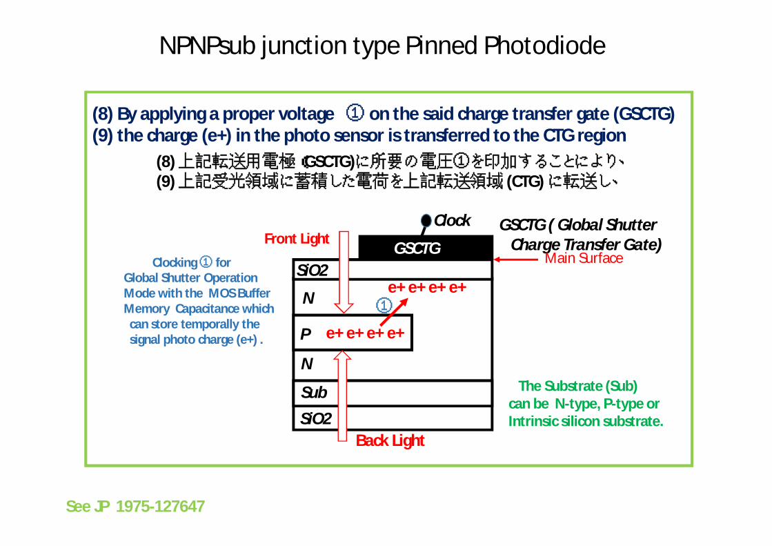
(8) By applying a proper voltage ① on the said charge transfer gate (GSCTG)(9) the charge (e+) in the photo sensor is transferred to the CTG region
(8) 上記転送用電極(GSCTG)に所要の電圧①を印加することにより、(9) 上記受光領域に蓄積した電荷を上記転送領域 (CTG) に転送し、
The Substrate (Sub) can be N-type, P-type or Intrinsic silicon substrate.
Front Light
SiO2
P
SiO2
N
N
Sub
GSCTG
Clock
Back Light
e+ e+ e+ e+
e+ e+ e+ e+
①
Clocking ① forGlobal Shutter Operation Mode with the MOS Buffer Memory Capacitance whichcan store temporally the signal photo charge (e+) .
GSCTG ( Global ShutterCharge Transfer Gate)
Main Surface
NPNPsub junction type Pinned Photodiode
See JP 1975-127647

(10) On the said charge transfer gate (GSCTG),(11) applying a different voltage ② from the said previous one(12) along the said main surface(13) the electric charge (e+) is to be transferred.(14) So defined photo image sensing structure is in the patent claim.
(10) 上記電荷転送用電極(GS)に(11) 上記所要の電圧とは異なるクロック電圧②を印加して(12) 上記基体の上記一方の主面に沿って(13) 電荷の転送を行うようにしたことを(14) 特徴とする固体撮像装置
The Substrate (Sub) can be N-type, P-type or Intrinsic silicon substrate.
Global Shutter
Front Light
SiO2
P
SiO2
N
N
Sub
Clock
Back Light
e+ e+ e+ e+ CTD
e+ e+ e+ e+
①
②
Clocking ② forCharge Transfer
Operation Modeto the adjacent CTD
Clocking ① forGlobal Shutter Operation Mode with the MOS Buffer Memory Capacitance whichcan store temporally the signal photo charge (e+) .
GSCTG ( Global ShutterCharge Transfer Gate)GSCTG
Main Surface
NPNPsub junction type Pinned Photodiode See JP 1975-127647

The Substrate (Sub) can be N-type, P-type or Intrinsic silicon substrate.
Front Light
SiO2
P
SiO2
N
N
Sub
Clock
Back Light
e+ e+ e+ e+ CTD
e+ e+ e+ e+
①
②
Clocking ② forCharge TransferOperation Modeto the adjacent CTD
Clocking ① forGlobal Shutter Operation Mode with the MOS Buffer Memory Capacitance whichcan store temporally the signal photo charge (e+) .
GSCTG ( Global ShutterCharge Transfer Gate)GSCTG
Main Surface
NPNPsub junction type Pinned Photodiode with Global Shutter Function and Back Light Illumination Scheme
See 1975-127647 ( October 23, 1975)
Japanese Patent by Yoshiaki Hagiwara at Sony
See JP 1975-127647
Sony Hagiwara Patent on the NPN junction/substrate type Pinned Photodiodewith a built-in Global Shutter Operation and Back Light Illumination scheme.
See JP 1975-127647
Visit https://www.j-platpat.inpit.go.jp/ and put the patent number 1975-127647

See JP 1975-127647
Visit https://www.j-platpat.inpit.go.jp/ and put the patent number 1975-127647

See JP 1975-127647
Visit https://www.j-platpat.inpit.go.jp/ and put the patent number 1975-127647
See JP 1975-127647
Visit https://www.j-platpat.inpit.go.jp/ and put the patent number 1975-127647
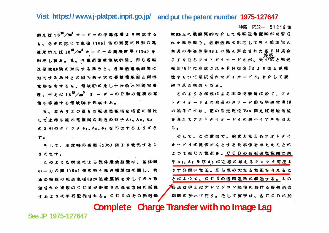
See JP 1975-127647Complete Charge Transfer with no Image Lag
Visit https://www.j-platpat.inpit.go.jp/ and put the patent number 1975-127647

See JP 1975-127647
Visit https://www.j-platpat.inpit.go.jp/ and put the patent number 1975-127647
See JP 1975-127647
Visit https://www.j-platpat.inpit.go.jp/ and put the patent number 1975-127647

See JP 1975-127647
Vertical Overflow (VOD)
Visit https://www.j-platpat.inpit.go.jp/ and put the patent number 1975-127647

See JP 1975-127647
Visit https://www.j-platpat.inpit.go.jp/ and put the patent number 1975-127647
See JP 1975-127647
Visit https://www.j-platpat.inpit.go.jp/ and put the patent number 1975-127647

See JP 1975-127647
Complete Charge Transfer with no Image Lag
Back Wafer Thinning for Back Light Illumination
Visit https://www.j-platpat.inpit.go.jp/ and put the patent number 1975-127647