japan offers an abundance of business opportunities - ivam · japan offers an abundance ... of an...
TRANSCRIPT

Volume 21 , No. 64, Summer 2016
come to make use of this unique centre and start or expand their business in Japan. With a total trading volume of EUR 37.2 bil-lion between Japan and Germany (EU-Japan: EUR 116.4 billion), Japan is both Germany’s and the EU’s second-largest trading partner in Asia after China. However, these pure fi-gures alone cannot nearly indicate how im-portant the Japanese market is for German companies. This February, the German Cham-ber of Commerce and Industry in Japan (AHK Japan) carried out a business climate survey among German companies that are located in Japan. Many of the companies that took part in this survey reported new possibilities going beyond merely doing business in Ja-pan: they have already managed to achieve a higher turnover outside than inside Japan – and expect even more in the future. These third-country collaborations with Japanese companies are steadily growing, above all in South East Asia, but in order to be success-ful in such projects, it proved necessary to be physically present in Japan.
Internationalization
While such third-country projects are mainly im-plemented with the well-known global players that have their produc-tion facilities all over the world, Japan at the same time has countless small and medium-sized companies producing state-of-the-art items that are often used in niche markets. It was
Japan offers an abundance of business opportunitiesSometimes neglected or even overlooked by international businesses, Japan is still the third-largest national economy. It is a country where tradition meets high-tech. Japan consists of 47 prefectures that all have their own regional characteristics. In general, however, it can be said that the Japanese heart of business is in Tokyo.
The automotive and aircraft industries can be found in the centrally-located Aichi Prefec-ture, the life science industry is in the Kansai region focusing on Osaka and Kobe, and ICT companies are mainly in northern regions like Hokkaido and Miyagi that offer a more suitable climate for data centers.
Demographic change
Japan and Germany have a lot in common: both are strong in automotive, mechanical engineering, medical technology, chemi-cals and pharmaceuticals, to mention but a few sectors. Both countries also face similar challenges like for instance the aging society. In Japan, already 25 % of its 127 million in-habitants are aged 65 and over. It is estimated that by 2040 even more than a third of the population will be in that age group. In order to tackle the problems this phenomenon entails, the Japanese government considers the medical technology sector a growth in-dustry and supports it. As the Japanese medi-cal device market relies heavily on imported products, it also offers good opportunities for foreign medical device makers. The annual sales amount of medical devices in Japan was JPY 2.67 trillion (ca. EUR 22.4 billion; 2013), 49 % of which were imported products.
Medical device market
Fukushima has always been home to many – also internationally well-known – medical device producers. To promote the develop- ment of medical devices, the prefecture in-itiated building the “Fukushima Medical Device Development Support Centre” which will be opened in November 2016. It will be the first hub centre in Japan for inte-grally supporting the implementation of medical devices from development to com-mercialization. Foreign companies are wel-
| Focus: Micro and Nano Industry in Japan|
Content
Japan offers an abundance of business opportunities 1
Editorial/Imprint 2
Micro metal injection molding to realize complicated small metal components 3
Microcondensation sensors for the Japanese market 4
Fukushima Prefecture – delivering next-generation medical devices 5
Micromachine Summit 2016 in Tokyo 6
Precision machining and micro processing 7
Company and product news 8
Trade shows and events 11
Petra Rehling
generally perceived in the past that Japan was a closed market and that Japanese companies rather stayed among themselves, but this changed drastically over the past years with growing globalization and the need for diversi- fication. The most recent trend to inter- nationalization was tragically triggered by the earthquake and subsequent tsunami in 2011. When many supply chains broke down and production came to a halt, it became obvious that a structural change was required.
www.ivam.eu
inno · Innovative Technologies - New Applications
Japan offers an abundance of business opportunities Page 1
Japan: a nation between tradition and high-tech. Source: IVAM

Welcome to the annual international issue of »inno«. This year, our internati-onal issue is dedicated to the micro and nano industry in Japan.
For more than ten years, IVAM has been regularly active in Japan, for example by maintaining contacts to partner associations like the Micromachine Center, which is introduced by Dr. Thomas Dietrich on page six. He also reports on the World Micromachine Summit 2016 in Tokyo this year, initiated by the Micromachine Center.
IVAM supports members worldwide concerning export issues, provides country-specific information, organizes delegation tours and initiates business-to-business contacts at trade shows and conferences like nano tech or Medical Creation Fukushima. Please find more details on current cooperations between German and Japanese Companies concerning medical technology on page five.
Another successful partnership between a German research institute and a Japanese company has just started: the CiS Forschungsinstitut für Mikrosensorik GmbH announced the signing of a distribution agreement with ESPEC Corp., a large manufacturers of environmental test chambers and reliability solutions. More Details can be found on page 4.
On page three the company Taisei Kogyo introduces a micro metal injection technique that enables the ultraprecise manufacturing of very small metal components that are used in medical equipment.
Furthermore you will find a more general view on the Japanese high-tech sector, provided by the Japan External Trade Organization (JETRO).
I wish you a pleasant reading! Best regards
Mona Okroy-Hellweg
Focus: Micro and Nano Industry in Japan
Editorial
»inno« Innovative Technologies – New Applications
Published by: IVAM e.V. Joseph-von-Fraunhofer Straße 13 D- 44227 Dortmund
Editors: Mona Okroy-Hellweg Iris Lehmann Dr. Thomas R. Dietrich
Contact: Mona Okroy-Hellweg
Phone: +49 231 9742 7089 Email: [email protected]
All articles in this issue are copy-right protected. Any further use or reprint must be approved by IVAM. Source reference is obligatory
Imprint
Even smaller Japanese companies now look for international partners to strengthen both their sales and also their purchasing channels. In this context, companies from the German “Mittelstand” are very popular to team up with. In order to promote the exchange between Japanese and foreign companies, the Japa-nese government through JETRO created the “Regional Industry Tie-up Program” (RIT). The program promotes two-way industrial exchange and collaboration between simi-larly structured regions in Japan and other countries. It includes delegation visits and matchmaking events in both regions. At
Volume 21 , No. 64, Summer 2016
present, there are 16 RIT projects world-wide, five of which are with Germany. The financial support for these programs is usually limited to three years, presuming that by then the contacts are already so well established that the two regions can continue their partner-ship without governmental support.
Cooperation between Fukushima and North-Rhine Westphalia
One example is the cooperation between Fukushima and North Rhine-Westphalia in the field of medical technology. In the past years, numerous small and medium-sized companies in Fukushima changed their strategy and diversified their portfolio, becoming suppliers to the medical industry. This opened new business opportunities to them. By joining the RIT Program, they also got access to German SMEs and are now in regular exchange. Although the official program has already ended, the collaboration between the regions continues quite successfully. While some Japanese companies managed to sell their products to Germany, others found a distributor, and yet another company entered a strategic partnership and started joint R&D. In November, a German delegation will be invited to Fukushima to exhibit at the medical devices fair “Medical Creation” and to deepen the relations.
Japan External Trade Organization(JETRO) www.jetro.go.jp
Japan offers an abundance of business opportunities Page 2
www.ivam.eu
Source: © boldg

Micro metal injection molding to realize complicated small metal components·Page 3
www.ivam.euVolume 21 , No. 64, Summer 2016
Micro metal injection molding to realize complicated small metal componentsTaisei Kogyo Co., Ltd. from Neyagawa-City specializes in manufacturing small metal components using original metal injection moulding (MIM) technology. The company started its operation in 1972 as a manufacturer of plastic injection molding and expanded in the 1990s to metal injection molding (MIM).
Taisei is a R&D focused company. Challeng-ing mass production of smaller and more complicated design components, introducing new materials and achieving high precision measurement are the main targets.
Multiple materials options
Compared to other MIM companies, Taisei is able to offer a wide range of material options such as stainless steel, titanium, titanium al-loy, copper, copper alloy, known as nickel silver, heavy alloy like tungsten or molybde-num alloy and precious metals like platinum, gold, and silver. This can be put into practice by composing the injection material, which is called feedstock, in-house. The feedstock is a mixture of metal powder and binder, which is mainly composed of resin. Since Taisei Kyo-go possesses a host of experience with resin from its plastic injection molding production, in-house feedstock production is one of its strengths. This original feedstock also enables mass production of smaller and more compli-cated design components than conventional MIM.
Micro internal helical gear
One example is the successful manufacturing of an internal helical gear with module 0.2. This size of internal helical gear was impos-sible to manufacture with other technologies such as CNC machining. Apart from the gear, the Japanese business Taisei has also achieved the world’s smallest metal check-valve pro-duction by MIM last year. The outer diameter
is 2.25 mm and the smallest wall thickness is 0.2 mm.
Taisei Kyogo’s proprietary MIM technology of-fers small surface roughness with Ra of 1-3 micrometres and Rz of 7-10 micrometres.
The MIM part achieves at least 95 % density compared to a machined part. Reduced rough-ness stems and high density are one of the re-sults from in-house binder development. While smaller metal powder grain size gives smaller roughness and higher density there are still some difficulties introducing finer metal pow-der in MIM production due to its larger surface area. Taisei Kogyo has developed a binder sys-tem especially for finer metal powder so they were able to employ it in production. Also, tolerance depends on the particle size of the metal powder, and Taisey Kyogo can achieve ±0.1% while ±0.5% in conventional MIM.
Sacrificial plastic molding
Another original technique is sacrificial plastic mold. The SP-mold is completely vaporised so the final product has exactly the same properties as normal MIM processed components. This technique enables mass production of complex designs such as curved hollow structures, undercuts, threads with hollow structure and other designs, which are difficult to manufacture by machining or other manufacturing methods.
The applications of MIM components vary from medical equipment, electronic equipment
to jewellery. However, half of Taisei Kyogo’s customers are in the medical equipment indus-try. The company has been producing medical components such as: micro forceps for mini-mally invasive surgery, endoscope parts, gears, nozzles, connectors and so on.
Taisei Kyogo has been not only developing manufacturing technologies but also developing and improving its quality assurance system. They own non-destructive measurement machines including X-ray CT scan systems, optical triple scan systems etc. Since their products become smaller and more complicated, improving the measurement system is crucial to maintain the quality. Taisey also offers measurement services in their Japanese research lab.
Taisei Kogyo Co.,Ltd, Neyagawa-City, Osaka, Japan www.taisei-kogyo.com
Izumi Nakamura
Micro internal helical gear Source: Taisei
Disposable micro forceps Source: Taisei
Connector with curved hollow structure Source: Taisei
www.ivam.eu
Microcondensation sensors for the Japanese market Page 4
Volume 21 , No. 64, Summer 2016
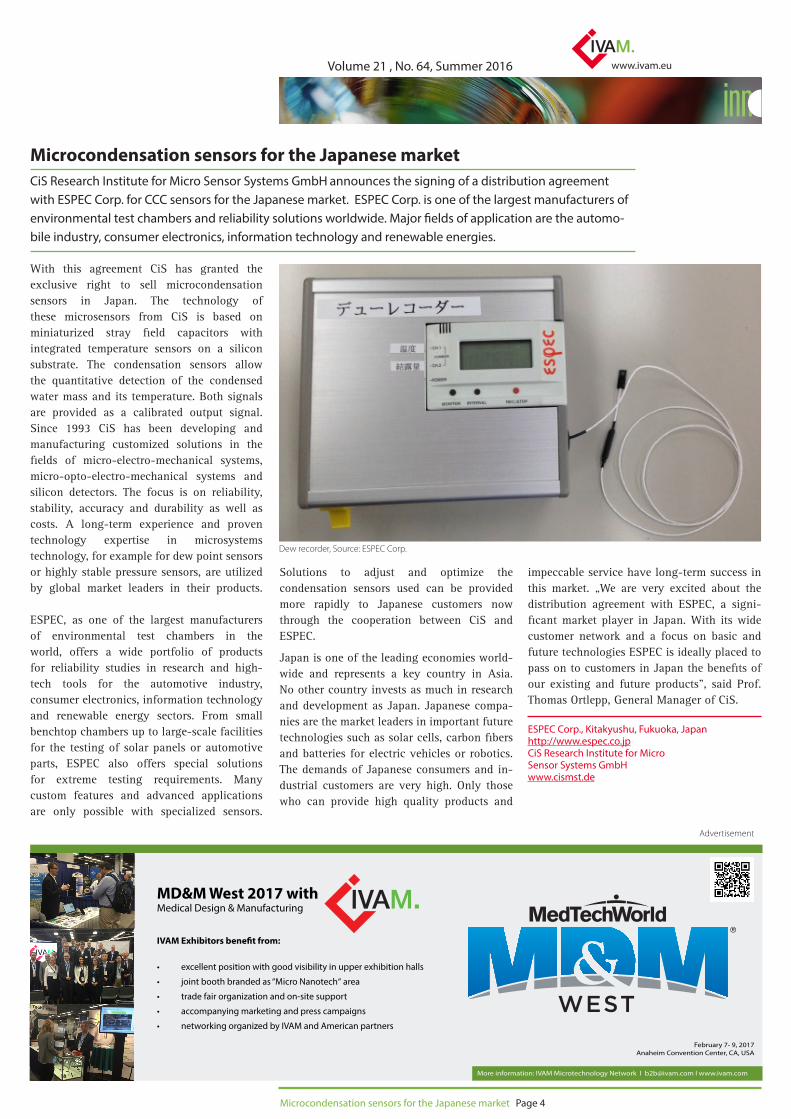
Microcondensation sensors for the Japanese marketCiS Research Institute for Micro Sensor Systems GmbH announces the signing of a distribution agreement with ESPEC Corp. for CCC sensors for the Japanese market. ESPEC Corp. is one of the largest manufacturers of environmental test chambers and reliability solutions worldwide. Major fields of application are the automo-bile industry, consumer electronics, information technology and renewable energies.
With this agreement CiS has granted the exclusive right to sell microcondensation sensors in Japan. The technology of these microsensors from CiS is based on miniaturized stray field capacitors with integrated temperature sensors on a silicon substrate. The condensation sensors allow the quantitative detection of the condensed water mass and its temperature. Both signals are provided as a calibrated output signal. Since 1993 CiS has been developing and manufacturing customized solutions in the fields of micro-electro-mechanical systems, micro-opto-electro-mechanical systems and silicon detectors. The focus is on reliability, stability, accuracy and durability as well as costs. A long-term experience and proven technology expertise in microsystems technology, for example for dew point sensors or highly stable pressure sensors, are utilized by global market leaders in their products. ESPEC, as one of the largest manufacturers of environmental test chambers in the world, offers a wide portfolio of products for reliability studies in research and high-tech tools for the automotive industry, consumer electronics, information technology and renewable energy sectors. From small benchtop chambers up to large-scale facilities for the testing of solar panels or automotive parts, ESPEC also offers special solutions for extreme testing requirements. Many custom features and advanced applications are only possible with specialized sensors.
Solutions to adjust and optimize the condensation sensors used can be provided more rapidly to Japanese customers now through the cooperation between CiS and ESPEC.
Japan is one of the leading economies world-wide and represents a key country in Asia. No other country invests as much in research and development as Japan. Japanese compa-nies are the market leaders in important future technologies such as solar cells, carbon fibers and batteries for electric vehicles or robotics. The demands of Japanese consumers and in-dustrial customers are very high. Only those who can provide high quality products and
impeccable service have long-term success in this market. „We are very excited about the distribution agreement with ESPEC, a signi-ficant market player in Japan. With its wide customer network and a focus on basic and future technologies ESPEC is ideally placed to pass on to customers in Japan the benefits of our existing and future products”, said Prof. Thomas Ortlepp, General Manager of CiS.
ESPEC Corp., Kitakyushu, Fukuoka, Japan http://www.espec.co.jp CiS Research Institute for Micro Sensor Systems GmbH www.cismst.de
Dew recorder, Source: ESPEC Corp.
MD&M West 2017 withMedical Design & Manufacturing
IVAM Exhibitors benefit from:
• excellent position with good visibility in upper exhibition halls
• joint booth branded as “Micro Nanotech“ area
• trade fair organization and on-site support
• accompanying marketing and press campaigns
• networking organized by IVAM and American partners
More information: IVAM Microtechnology Network I [email protected] I www.ivam.com
February 7- 9, 2017Anaheim Convention Center, CA, USA
Advertisement

Fukushima Prefecture – Delivering Next-Generation Medical Devices Page 5
www.ivam.eu
Fukushima Prefecture – delivering next-generation medical devicesWhat is the first thing that comes to ones mind when hearing the name “Fukushima”? The Great East Japan Earthquake or the Fukushima Daiichi nuclear disaster may be the first events people think of. This makes it all the more suprising that Fukushima Prefecture is also a well-known producer of medical devices and its parts and components.
After the Great Earthquake, the medical indus-try has become a top priority project of the Prefectural Government for the recovery of Fukushima, and now the prefecture aims to become one of the leading sites in clustering medical industries.
Economic situation and cooperations
According to data from 2014, Fukushima has the highest sales figures of parts and components for medical devices, the highest sales figures of medical related OEM pro-duction and the third highest sales figures in the production of completed medical devices throughout Japan. These high turnovers are possible due to Fukushima as the choice of location of leading companies from abroad and many local SMEs inside the prefecture. In 2014, Fukushima Prefecture has signed a Memorandum of Understanding (MOU) in the fields of medical devices with the State of North Rhine-Westphalia (hereafter referred to as NRW) in Germany to strengthen the part-nership between the state and the prefecture. Dr. Thomas Dietrich, CEO of IVAM Microtech-nology Network, was appointed as official co- ordinator to support business matchings between companies from Fukushima and NRW. As part of the signed MOU, companies from NRW are regularly exhibiting at the “Medical Creation Fukushima” in Fukushima Prefecture, and in return, companies from Fukushima are exhibiting at the MEDICA/COMPAMED, hosted in Düsseldorf. This November, eight companies from Fukushima will exhibit at the “Fukushi-ma booth” at COMPAMED again.
Medical Devices Development Support Centre
Furthermore, Fukushima plans to open the new Fukushima Medical Devices Development Support Centre in November 2016. The center offers electrical safety tests, environmental testing and many more beneficial testing for the development of medical devices. The installation of simulated operation rooms and a training room inside the center makes it possible to train highly qualified staff, to get assistance by specialists and to get in touch with consultants. A MOU with TÜV Rheinland, a third party certification body from Cologne, for further cooperation in this field was signed last year in October. Every necessary step housed under one roof, the Fukushima Medical Devices Development Support Centre wants to be a perfect partner for companies worldwide to get ready and to meet all Japanese
regulations and to introduce products to the Japanese market.
Subsidies and events
In addition, the Fukushima Prefecture offers regularly attractive subsidies for foreign com-panies who want to enter the Japanese market by starting their first business activities in Fukushima. Eligible are companies related to the fields of medical devices, renewable energies, and robotics. The total amount of subsidy for each company is up to 28 million yen per year and can be used e.g. for renting office spaces, registration fees, or personnel expenses.
Another activity is the cooperation with foreign hospitals. Therefore, a two-day sym-posium at the University Hospital Essen takes place September1-2, 2016. The symposium’s title is “Japanese and German Cutting Edge Technologies for Patient Care - 1st NRW-Fukushima Joint Symposium on Advances in Medicine”. Vice-Governor Toshiyuki Hata from Fukushima Prefecture will inform the audience about the present conditions of Fukushima and its strategies and plans for the creation of medical, renewable energy and robotic related industries. The symposium is open to the general public and free of charge.
Commerce, Industry & Labour Department Fukushima Prefectural Government http://www.pref.fukushima.lg.jp
Volume 21 , No. 64, Summer 2016
Go Theisen
Medical Devices Development Support Centre Source: Fukushima Prefectural Government
Companies from NRW are regularly exhibiting at the “Medical Creation Fukushima” (right) and companies from Fukushima are exhibiting at the COMPAMED (left) Source: Fukushima Prefectural Government

Micromachine Summit 2016 in Tokyo Page 6
www.ivam.euVolume 21 , No. 64, Summer 2016
Micromachine Summit 2016 in TokyoThe 22nd Micromachine Summit took place from May 24-27, 2016 in Tokyo, Japan. This annual conference was laun-ched in Kyoto by the Micromachine Center in 1995. Since then, delegations from most major industrial countries show the latest developments in micro- and nanotechnology from the different regions of the world once a year.
This year, 25 countries were represented at the Micromachine Summit, from Japan, Europe and the Americas. The focus was „Aging Society and Health (Medical Applications of MEMS)“. Once again, the Micromachine Summit reflected the focus for the high-tech industry in the industrial countries. Interestingly, the issues which countries have to face are very similar all over the world. Japan, like Germany, has a lot of problems with the aging society. More and more older people require more individual care, which has to be supported by the health system. The costs are rising continuously and can be financed only with the development of high-tech products, which help to reduce costs and the number of required nurses and hospitals. Prof. Isao Shimoyama (University of Tokyo) reportes on the latest development within the Japanese high-tech industry and research. The Japanese government has launched a new Science and Technology Plan „Super Smart Society 5.0“, focussing the Internet of Things. In October 2015 an „Acceleration consortium“ was founded in Japan under the guidance of the National Institute of Information and Communications Technology (NICT). Almost 2,000 members, companies, research institutions and government representatives are working together, mainly financed by the Ministry of Internal Affairs and Communications and the Ministry of Economy, Trade, and Industry. The project plan is to generate concerted actions, combining the strengths of each partner and to coordinate joint activities. A key point is the standardization, in particular of hardware
and software interfaces, and the development of new business models and generation of model businesses. First projects focus on the realization of inexpensive home security, a trading system for real-time sensor data distribution, or the commercialization of the data exchange market in Japan.
The IoT program has been complemented in May 2015 by the „Robot Revolution Initiative“. In Japan robots are already used in all parts of daily life and accepted and welcome (in con-trary to European countries) by the majority of the population. A typical example are robot
nurses in hospitals, which are already used for distribution of drugs or in the care of dementia patients. Besides the health care market, a ma-jor effort is made in the field of autonomous vehicles in the automotive sector. Also in the industrial sector, the use of robots is promoted by standardization, by projects for increasing the safety and security of robots or in the field of artificial intelligence. Japan works closely with foreign organizations such as the Indus-trial Internet Consortium of the United States or the Industry 4.0 initiative in Germany. These programs are supported by the Japanese go-vernment with $ 100 million in the year 2016.
The Micromachine Summit ended with a tour to some companies and research institu-tions. The Fujikin Corp. Group demonstrated its microtechnological flow sensors and sys-tems for space applications as well as for fish breeding. The University of Tsukuba showed farms for the production of algae for energy and cosmetic products. In the coming year the conference will be hosted in Barcelona by the Spanish delegation.
IVAM Microtechnology Network, www.ivam.com
Dr. Thomas R. Dietrich
Change in the number of jobs in industries with the highest increase and decrease in the five-year period from 2007 to 2012 Source: Official Statistics of Finland (OSF): Employment [e-publication]. ISSN=2323-6825. Background information on unemployed persons 2012. Helsinki: Statistics Finland [referred: 26.7.2015].
About Micromachine Center
The Micromachine Center is a Japanese organization that takes care of the
national development and promotion of microtechnology. For this work
they founded the MEMS Industry Forum (MIF) to accelerate industrialization
of MEMS / micro-nanotechnologies. It works on the recommendation of
industrial / technical policy, on the proposal of R&D projects, and on standardization. It supports
Japanese companies with lobbying, through contacts with foreign associations or by information
within conferences and seminars. The Micromachine Center annually organizes the conference-
exhibition „Nano Micro Biz“ in Yokohama and is represented in many international fairs. Since
many years, IVAM has been cooperating with this high-tech network for the benefit of companies
from both countries.

Injection-molded structural electronics Page 7
www.ivam.eu
Precision machining and micro processingMATS TECH GmbH of Germany represents M.TECH Co., Ltd. in Japan as sales and marketing office for the European region.
Minimum φ0.05mm thinness by cutting
M.TECH Co., Ltd. and MATS TECH GmbH spe- cialize in precision machining and micro processing using numerical control la-the.The company has developed a unique long-thin processing technology in-house. The technology makes it possible to pro-cess down to φ0.05mm thinness and length ten times of its diameter with various ma-terials such as iron, stainless steel, copper alloy or titanium. Picture 1 shows Φ0.08 mm × 0.8mm on the top of Φ0.5 mm material by titanium.
Real-time correction control with a CCD camera
As the work pieces are so thin, it is easy to imag-ine that they will get bent, turned or broken during the process. In order to solve this problem, the used equipments have an installed CCD camera to measure the distance between the blade and the workpiece to calculate the depth for required cuts and to inform the system. This allows a real-time correction control and thereby a highly precise processing of micro-long parts with numerical control lathe without grinding - contrary to conventional methods
which may cause the parts to bend or break.
In 2012 M.TECH Co., Ltd. was selected for a supporting industry project sponsored by the Ministry of Economy, Trade and Industry (METI) of Japan. The real-time correction con-trol system was developed during this project.
Customized equipment
The factory is furnished with the latest equip-ment including 32 CNC lathes, one contour measuring device, two roundness testers, one digital microscope, etc. Those machines have been customized and improved according to long history and experiences of M.TECH Co., Ltd. and enable the unique processing techno-logy.
MATS TECH GmbH was established in October 2013 in Dusseldorf, Germany, in order to ex-pand the services in automotive and medical equipment industries and to provide the cut-ting-edge machining and fine processing tech-nology even wider. In addition to M.TECH’s business as a contractor, MATS TECH im-ports outstanding Japanese products, such as small numerical control lathes, jigs and power conserving electric apparatus and hand pres-ses.
MATS TECH GmbH/ M.TECH JAPAN Co., Ltd. http://m-tech61.main.jp/en/
Kanako Minami
Volume 21 , No. 64, Summer 2016
MICRO-NANO-AREAKey Enabling Technologies at HANNOVER MESSE 2017
Micro- and Nanotechnology, MEMS, Photonics and Advanced Materials
• concentration of exhibitors with micro and nano products
• higher quantity and quality of leads
• effective exchange between exhibitors
• organized business meetings and networking
• co-operation of Deutsche Messe and IVAM
• advertising through Deutsche Messe and IVAM
More information: IVAM Microtechnology Network I [email protected] I www.ivam.com
April 24 - 28, 2017
Advertisement
Picture 1

Company and product news Page 8
www.ivam.euVolume 21 , No. 64, Summer 2016
New process tool for the inspection of probe cards generates positive response from semiconductor industry
NanoFocus AG launched the new measuring system μsprint hp-opc 3000 for the optical inspection of probe cards in May and June 2016. μsprint hp-opc 3000 is applied for the inspection of probe cards, which are special test devices used for standard function tests of wafers. Since wafer testing can only take place after the functional structures on a wafer are fully manufactured, damage of wafers during testing represents a significant economic loss. At this point, the inspection system μsprint hp-opc 3000 enables a novel and innovative process step. The measuring system ensures that the wafers are in sound condition after testing. It consequently contributes to reducing operational costs, minimizing yield losses as well as increasing quality in wafer production. „We are pleased about the positive feedback of industry experts. It proves that μsprint hp-opc 3000 is a tailor-made solution to current requirements and expectations of wafer manufacturers,” says Martin Kunz, Head of Business Unit Semiconductor at NanoFocus. The potential and advantages of the tool were recognized in particular for wafer test locations with large-volume throughput and for the manufacturing process of probe cards. Additionally, the compatibility to existing probe card testing processes was positively received. A pilot system already is successfully installed at a renowned manufacturer of semiconductor elements. Further orders are expected in the third quarter of 2016.
NanoFocus AG, Claudia Delto, Email: [email protected], www.nanofocus.com
Source: Sensirion AG
Berliner Glas expands its coating capacity and expertise
The Berliner Glas Group has recently expanded its coating center at the Berlin site to a customized APS system (APS = advanced plasma source). The new coating system facilitates the production of highly sophisticated coatings, consisting of a plurality of individual layers, for example, edge filters, highly reflective layers (dielectric mirrors) or laser-resistant layers. These coatings are used, amongst others, in medical technology, space communications and the telecommunications industry. Due to the new APS system the capacity for customer applications is increased and the development of new technologies within the Berliner Glas Group is accelerated. The optical monitoring system (OMS 5000) – also called direct monitoring – determines the optical thickness of the growing single layer during the coating process, compares it with the set values from the layer simulation in real time and corrects any errors as needed. This OMS enables Berliner Glas to realize edge lengths with an accuracy of +/- 0.5 % at 650 nm. This opens the door to a wider market as this ensures compliance with increasingly stringent specifications. The „Coating & Surfaces“ division of the Berliner Glas Group develops and manufactures sophisticated coatings for individual requirements of customers. The spectral range extends from the UV to the infrared range. With this new APS system, the Berliner Glas Group has invested in the future, created the basis for further growth and ensures continued compliance with the ever increasing demands of the market and customers.
Multifunctional prism. Source: Berliner Glas
New ultra-small digital humidity sensor: simplicity meets proven performance
Sensirion, manufacturer of humidity, temperature and flow sensor solutions, presents its second generation WLCSP (wafer-level chip-scale package) humidity sensor: the SHTW2. The sensor comes in a flip chip package – an established technology that represents one of the simplest and smallest possible ways of packaging a semiconductor chip and results in a tiny footprint of 1.3 x 0.7 x 0.5 mm3. The SHTW2 also pioneers a new category of ultra-small humidity sensors suitable for applications with the tightest space constraints. The sensor is based on Sensirion’s CMOSens Technology, which offers a complete sensor system on a single chip with a digital I2C interface. The sensor is fully calibrated and covers a humidity measurement range of 0 to 100 % RH and a temperature measurement range of -30 to 100 °C, with a typical accuracy of ± 3 % RH and ±0.4 °C. The operation voltage of 1.8 V and the low power consumption make the SHTW2 suitable for integration in consumer electronics that run on the tightest power budgets, such as mobile phones, wearables and Internet of Things (IoT) applications. Tape and reel packaging and suitability for standard SMD assembly processes ensure the SHTW2 is ideal for high-volume applications. In combination with Sensirion’s complete solution approach, the new SHTW2 humidity sensor is meant for highly reliable humidity and temperature measurement in consumer electronics and IoT applications. The complete solutions approach means that Sensirion not only provides sensor hardware, but also supports customers with hardware and software integration as well as by developing algorithms and use cases.
μsprint hp-opc 3000 for the inspection process of probe cards in wafer production Source: NanoFocus AG
Sensirion AG, Email: [email protected], www.sensirion.com
Berliner Glas, Iris Teichmann, Email: [email protected], www.berlinerglas.com
Company and product news

Company and product news ·Page 9
www.ivam.euVolume 21 , No. 64, Summer 2016
Fraunhofer IMS develops extremely low-noise read out ASIC for capacitive sensors
Extremely low-noise, highly precise: those are the prominent characteristics of the IMS-CAP51. The product adds these “merits” to the read-out of capacitive sensors, for example of acceleration MEMS. Its special talents come into effect where highly accurate measured data is of great importance: for example seismic measurements for the early detection of earthquakes. The fundamental mode of operation: the IMS-CAP51 of the Fraunhofer Institute for Microelectronic Circuits and Systems IMS is connected to a capacitive acceleration MEMS on a printed circuit board. Acceleration forces affect this MEMS, which hence generates a capacity gap. The ASIC converts the measured capacity gap into voltage. Eventually, this voltage is translated into a digital measurement value by an analog-to-digital converter. The ASIC can be delivered with an analog-to-digital converter if requested.“The core task was to develop a read-out circuit where the input-based noise is extremely low” Dr. Alexander Utz, head of the project ASIC development, describes the initial situation. Because: the higher the noise, the less reliable the measurement results. The task has been solved after two years of time. The Fraunhofer team has achieved a very low input-based noise with a concurring broad range (0 Hz - 15 kHz). The input-based noise is located at values beneath 50 zF/rt-Hz- therefore the new IMS-CAP51 of the Fraunhofer IMS from Duisburg holds the world record. The experts obtained those results by executing the capacity-voltage conversion as a AC-paired Chopper-amplifier. “With this method, the 1/f-noise, which is dominant at semiconductor circuits and is especially disruptive at lower frequencies, can be confined, respectively suppressed effectively”, explains Utz. Now the ASIC can be applied where especially delicate measurements with weak signals have to be carried out. Customer-specific realizations for special requirements are gladly implemented by the Fraunhofer IMS in accordance with the customer. This opens up diverse application fields. Applied in early detection systems for earthquakes or Tsunamis it can supply information about vibrations in the earth early and precisely. Such seismic measurements are also helpful to the search of oil and gas fields. Vibration profiles are recorded, which allow conclusions about potential oil and gas resources. The ASIC can also be applied to measure vibration in course of monitoring building foundations. In connection with a positioning sensor, the ASIC can also be utilized for the alignment of antennas by using the effects of earth’s gravity onto the sensor.
Fraunhofer IMS, Verena Sagante, Email: [email protected], www.ims.fraunhofer.de
International companies showcase their innovations at Medical Manufacturing Asia in Singapore
Singapore is the door to enter the Asian markets because it offers the unique chance to get in contact with potential customers and suppliers from Japan, China, Taiwan and Korea at the same time. From August 31 to September 2, 2016, the MEDICAL MANUFACTURING ASIA (MMA), a specialist trade show for medical manufacturing, will again take place in Singapore, co-located to MEDICAL FAIR ASIA. For manufacturers and suppliers, this marketplace provides a perfect business platform to present the latest innovations, products and services and network with an international yet targeted audience. The main topics of MMA are, for example, innovations from micro- and nanotechnology like modules and components for medical technology, lab-on-a-chip technology, inspection equipment and testing services as well as assembly, automation and production technology. Process technology, biocompatible materials, coating and functional surfaces also play an important role. The IVAM Microtechnology Network will attend the MMA once more with a joint pavilion and will present the session about “High-tech for Medical Devices“ at the co-located experts forum.
Source: MMA, Finetech GmbH & Co. KG, Microsystems Enginee-ring Solutions
MEMS & Sensors Industry Group Conference Asia 2016
Recognizing the massive growth potential of micro-electro-mechanical systems (MEMS) and sensors in Internet of Things (IoT) applications, MEMS & Sensors Industry Group (MSIG) will hold its third annual MEMS & Sensors Industry Group Conference Asia in Shanghai, China on September 13-14, 2016. Held in partnership with Shanghai Industrial Technology Research Institute (SITRI) and co-located with SENSOR CHINA, “The Internet of MEMS and Sensors Today and the Internet of TSensors Tomorrow” is a two-day conference focused on near- and long-term opportunities for MEMS and sensors in the IoT. MSIG and its members will also participate in a two-day exposition at SENSOR CHINA. As the commercialization of MEMS and sensors has become ever more present, companies are positioning themselves as both hardware and software providers, whereby they are not just selling chips, but also the algorithms and sensor fusion to simplify system integration, maximize value, and remain competitive. MSIG’s Conference Asia will showcase companies in Asia addressing this holistic approach to value with products and services currently available, or on the cusp of commercialization. While the first day of the conference will consist of general session presentations offering examples of how to maximize value from the MEMS and sensors supply chain, the second day offers a more long-term approach, with a focus on products and solutions that support the use of a trillion sensors (TSensors™) by 2020. These presentations encompass products that intend to meet the demand of emerging MEMS and sensors and to meet the impending demand of the Internet of Things/Everything (IoT/E) for connected devices. For a full list of conference speakers and panel sessions, please visit the MSIG Conference Asia web site: http://msigevents.org/asia-2016/
Proportion: The „IMS-CAP51“ sensor on a fingertip Source: Fraunhofer IMS
MEMS & Sensors Industry Group, Andy Knopes, Email: [email protected], www. http://memsindustrygroup.org/
Company and product news
IVAM, Orkide Karasu, Email: [email protected], www.ivam.eu

Company and product news·Page 10
www.ivam.eu
Company and product news
Microbiology meets micro injection molding : Labs on chip – the smallest laboratories worldwide
z-microsystems´ unique core competence is to support customers to transfer their individual designs of microfluidic devices into a part which is injection moldable. To get a first impression in most cases it makes sense to produce prototypes. Therefore, z-microsystems has the prototyping capabilities as e.g. micro-milling, stereolithography or special quick-toll and rapid injection molding technique in-house. These pilot molds are designed as a preliminary stage for the production mold. After first sampling, the pre-production/pilot phase is carried out before taking the process into full mass production under clean room conditions.
A prime example came out of the partnership with the Swiss company rqmicro. rqmicro developed a patho-gen separation and detection technology that delivers accurate results in less than one hour. By separating infectious bacteria with magnetic nanoparticles out of the sample matrix and quantifying them on the single cell level, it is possible to achieve superior test performance in water or food samples within minutes. rqmicro´s users benefit from ultrafast separation of microorganisms from complex samples, real-time detec-tion and quantification and automated workflow for on-site testing. The technology base to achieve these goals is microfluidics. Microfluidics is a multidisciplinary field intersecting engineering, physics, chemistry, biochemistry, nanotechnology, and biotechnology. rqmicro uses a combination of microfluidics and high gradient magnetic fields that allows target cells to be separated from a sample with high efficiency, using immunomagnetic separation (IMS) in contrast to conventional column-based methods. Conventional IMS systems are labor-intensive and lead to lower purity – especially in natural samples, where contaminants have a higher tendency to be stuck in the column.
Successful start for the international high-tech conference “Health Business Connect”
IVAM Microtechnology Network and its French partner network Pôle des Microtechniques (PMT) organized a two-day meeting for companies from the high-tech sector with the focus on medical technology, which took place on July 11-12 in Besançon, France. The purpose of the event was the international promotion of cooperation between manufacturers of components and devices, software companies and other companies from the field of medical technology, as well as joint projects, exchange of experience and possibilities for entering the medical technology market.
The first day was dedicated to the cooperation of manufacturers of components and medical devices. Que-stions like “What kind of data distributors have to share with their clients and what kind of data can be held back for the protection of proprietary know-how?” were central. Renowned device manufacturers like Karl Storz or Molex discussed their various viewpoints with component manufacturers like AEMtech, Jenoptik or Statice. Besançon is a center of the French microtechnology industry, the venue of France’s biggest micro-technology trade fair MICRONORA and the location of the well-known research institute for microtechnology femto-st, which is located at the technology center temis, where the event Health Business Connect took place. After the discussion of principal questions at the first day of the event, the second day was mainly assigned to almost hundred B2B meetings between the participants. Many companies decided to participate in Health Business Connect particularly because of these meetings, which had been organized prior to the event. Due to the large demand, many further talks took place during the extensive accompanying networ-king program. The participants of the event, who came from 10 countries in Asia, Europe and North America, were fully satisfied with the organization and the results of the event. Pierre Vivien (CEO of PMT) and Thomas Dietrich (CEO of IVAM) both agree: „The mixture of traditional conference, B2B meetings, company visits and networking program was the recipe for success of this event“. PMT and IVAM are planning to expand the cooperation and agreed to arrange a followup conference at Dortmund, Germany next year.
z-werkzeugbau-gmbh, Markus Ebster, Email: [email protected], www.z-microsystems.com
The plastic micro-injection-molded consumable allows 4 samples to be prepared simultaneously (see picture). Source: z-werkzeugbau-gmbh
Volume 21 , No. 64, Summer 2016
IVAM, Orkide Karasu, Email: [email protected], www.ivam.eu
Source: IVAM
SENperc PV awarded at SNEC Show 2016
SENTECH presented the new, innovative SENperc PV – a metrology tool for quality control in PERC solar cell manufacturing. Al2O3/SiNx layer stacks and single films for passivation of PERC solar cells are measured. The SENperc PV was introduced for the first time in China. It was awarded at the on-site session of the SNEC Show as one of the “Top 10 Highlights” as innovative product launch in 2016. Dr Gruska, Marketing Manager at SENTECH, introduced the new quality control tool. The SENperc PV measures thickness and refractive index of single Al2O3 and SiNx films and Al2O3/SiNx layer stacks on the back side of PERC solar cells. Easy recipe-based operation and statistical process control make the SENperc PV the ideal tool for quality control of PERC passivation layers. Direct and long-term feedback to the operator for immediate intervention drew attention to the new SENTECH tool at SNEC PV Power Expo. The SNEC PV Power Expo is important to SENTECH as one of the world leading photovoltaic exhibitions. This annual event takes place in Shanghai, China and attracts several thousands of visitors yearly. On 150,000 sqm more than 1500 exhibitors presented innovative solutions and new products for the production of clean and sustainable energy.
Source: SENTECH Instruments GmbHSENTECH Instruments GmbH, Email: [email protected], www.sentech.de

IVAM trade shows and events
www.ivam.eu
Medical Manufacturing Asia 2016 August 31 - September 2, 2016, Singapur, SG Manufacturing Processes for Medical Technology www.ivam.de Dortmunder MST-Konferenz September 20-21, 2016, Dortmund, DE German conference on “MST 4.0 - digital and networked microtechnology“ www.ivam.de
‘Unternehmertreffen Medizintechnik NRW - JAPAN‘ October 24, 2016, Bochum, DE “Distribution Channels in Japan“ A German Workshop by NRW.International GmbH LaserForum 2016 November 3, 2016, Hanover, DE German conference on „Medical Laser Applications“ www.ivam.de COMPAMED November 14-17, 2016, Dusseldorf, DE International leading trade fair for suppliers of medical manufacturing. IVAM will present the Product Market “High-tech for Medical Devices“ as well as the “COMPAMED HIGH-TECH FORUM“. www.ivam.de
Focus Group Wearable Electronics November 14, 2015, Dusseldorf, DE www.ivam.de Medical Creation Fukushima 2016 November 25-26, 2016, Koriyama City, JP Design and production of medical devices www.ivam.de MD&M West 2017 February 7-9, 2016, Anaheim CA, USA IVAM organizes a joint pavilion at the focus area MicroNanoTechnology www.ivam.de nano tech 2017 February 15-17, 2016, Tokyo, JP IVAM organizes the German pavillion. www.ivam.de IVAM High-tech Summit March 23, 2017, Dortmund, DE Experts conference on key enabling technologies Co-located to annual general meeting of IVAM HANNOVER MESSE April 24-28, 2017, Hanover, DE The world‘s largest industrial fair - IVAM will present the new MICRO-NANO-AREA www.ivam.de COMPAMED Spring Convention May 3, 2017, Frankfurt am Main, DE Annual German conference on medical device technology
IVAM trade shows and events · Page 11
Volume 21 , No. 64, Summer 2016
Click at the image to read the repective issue Sources: »inno« 53: Robert Bosch Healthcare GmbH/ »inno« 54: IMTEK & PI miCos GmbH/ »inno« 55: Photograph Fred Kamphues/ »inno« 56: Sensirion AG/»inno« 57: © vschlichting - Fotolia.com/ »inno« 58: Specialty Coating Systems/»inno« 59: Cicor/»inno« 60: © svedoliver - Fotolia.com/ »inno« 61: VTT- Technical Research Centre of Finland/ inno« 62: © Photographee.eu fotolia.com/ »inno« 63: airFinity »inno« 64: Taisei Kogyo Co., Ltd.
Would you like to read »inno« regularly? »inno« is published three times per year. »inno« is pu-blished three times per year. The magazine is published in German every spring and autumn. Since 2013, every summer issue of the magazine is published as internatio-nal edition in English. At www.ivam.de/inno you can read, download, subscribe or unsubscribe for the digital edition. Printed copies of »inno« are available for free at all IVAM trade shows and events.
»inno« 54 Robotik
»inno« 55 The Netherlands
»inno« 56 Medizintechnik
»inno« 57 Automobil-Industrie
»inno« 58 USA
»inno« 59 Medizintechnik
»inno« 60 Industrie 4.0
»inno« 61 Finland
»inno« 53 AAL/Medizintechnik
»inno« 62 Medizintechnik
»inno« 63 Haus- und
Gebäudetechnik
»inno« 64 Japan

MICROTECHNOLOGY NETWORK
マイクロテクノロジー協会(IVAM)は、マイクロ・ナノ工学、新素材、光学・光子分野に携わる会員企業により構成される国際的ネットワークです。IVAMでは、革新性の高い技術や製品をもちながら、海外市場に進出しにくい中小企業を後押しすることを大きな使命としています。これまでに、世界各地の企業や研究機関がIVAMのサポートにより先端技術市場を開拓し、新たな業界基準を確立してきました。また、見本市への共同出展、ワークショップ、セミナー、定例会などを企画・開催することにより、IVAMは国際的な協力関係を築いてきました。
最先端の製品やサービスの普及にはその内容説明が不可欠ですが、IVAMは自らをメーカーとユーザーとのコミュニケーションの橋渡し役であると考えています。よって、当協会の主な任務は、会員間での情報交換、共同プロジェクト、交流を促すことによりシナジー効果を生み出し、業界として潜在顧客に働きかけていくことにあります。
Sources: IVAM, Micromotion GmbH, Bernd Müller for HSG-IMIT, © CDA GmbH, Häcker Automation GmbH
IVAM マイクロテクノロジー協会Joseph-von-Fraunhofer-Straße 13D-44227 Dortmund電話: +49 (0) 231 9742 168
www.ivam.com
Advertisement