jackrabbit (bl1800) - acierta it solutions con todo/dcrabbit_9... · 4 jackrabbit (bl1800) 1.4 ce...
TRANSCRIPT
Jackrabbit (BL1800)C-Programmable Single-Board Computer
User’s Manual019–00067 • 030131–E

Jackrabbit (BL1800) User’s Manual
Part Number 019-0067 • 030131–E • Printed in U.S.A.
©2000–2003 Z-World Inc. • All rights reserved.
Z-World reserves the right to make changes andimprovements to its products without providing notice.
TrademarksRabbit 2000 is a trademark of Rabbit Semiconductor.
Dynamic C is a registered trademark of Z-World Inc.
Jackrabbit (BL1800)
Z-World, Inc.
2900 Spafford StreetDavis, California 95616-6800
USA
Telephone: (530) 757-3737Fax: (530) 753-5141
www.zworld.com

TABLE OF CONTENTS
Chapter 1. Introduction 11.1 Features .................................................................................................................................................11.2 Development and Evaluation Tools......................................................................................................21.3 How to Use This Manual ......................................................................................................................3
1.3.1 Additional Product Information ....................................................................................................31.3.2 Online Documentation ..................................................................................................................3
1.4 CE Compliance .....................................................................................................................................41.4.1 Design Guidelines .........................................................................................................................51.4.2 Interfacing the Jackrabbit to Other Devices..................................................................................5
Chapter 2. Subsystems 72.1 Jackrabbit Pinouts .................................................................................................................................8
2.1.1 Headers..........................................................................................................................................82.2 Digital Inputs/Outputs...........................................................................................................................9
2.2.1 Digital Inputs.................................................................................................................................92.2.2 Digital Outputs............................................................................................................................102.2.3 Bidirectional I/O .........................................................................................................................12
2.3 A/D Converter.....................................................................................................................................132.4 D/A Converters ...................................................................................................................................15
2.4.1 DA1.............................................................................................................................................162.4.2 DA0.............................................................................................................................................18
2.5 Serial Communication ........................................................................................................................202.5.1 RS-232 ........................................................................................................................................202.5.2 RS-485 ........................................................................................................................................202.5.3 Programming Port .......................................................................................................................22
2.6 Memory...............................................................................................................................................232.6.1 SRAM .........................................................................................................................................232.6.2 Flash EPROM .............................................................................................................................23
2.7 Other Hardware...................................................................................................................................242.7.1 External Interrupts.......................................................................................................................242.7.2 Clock Doubler .............................................................................................................................242.7.3 Spectrum Spreader ......................................................................................................................25
Appendix A. Specifications 27A.1 Electrical and Mechanical Specifications ..........................................................................................28A.2 Jumper Configurations.......................................................................................................................30A.3 Conformal Coating.............................................................................................................................32A.4 Use of Rabbit 2000 Parallel Ports ......................................................................................................33
Appendix B. Prototyping Board 37B.1 Mechanical Dimensions and Layout..................................................................................................38B.2 Using the Prototyping Board..............................................................................................................39
B.2.1 Demonstration Board .................................................................................................................40B.2.2 Prototyping Board ......................................................................................................................42
User’s Manual

Appendix C. Power Management 45C.1 Power Supplies .................................................................................................................................. 45C.2 Batteries and External Battery Connections...................................................................................... 48
C.2.1 Battery Backup Circuit .............................................................................................................. 49C.2.2 Power to VRAM Switch ............................................................................................................ 50C.2.3 Reset Generator.......................................................................................................................... 50
C.3 Chip Select Circuit............................................................................................................................. 51
Appendix D. Alternate Use of the Programming Port 53
Notice to Users 55
Index 57
Schematics 59
Jackrabbit (BL1800)
1. INTRODUCTION
The Jackrabbit is a high-performance, C-programmable control-ler with a compact form factor. A Rabbit 2000™ microprocessoroperating at 30 MHz provides fast data processing.
1.1 Features
• 30 MHz clock
• 24 CMOS-compatible I/O
• 3 analog channels: 1 A/D input, 2 PWM D/A outputs
• 4 high-power outputs (factory-configured as 3 sinking and 1 sourcing)
• 4 serial ports (2 RS-232 or 1 RS-232 with RTS/CTS, 1 RS-485, and 1 CMOS-compati-ble)
• 6 timers (five 8-bit timers and one 10-bit timer)
• 128K SRAM, 256K flash EPROM
• Real-time clock
• Watchdog supervisor
• Voltage regulator
• Backup battery
Appendix A provides detailed specifications for the Jackrabbit.
User’s Manual 1

Three versions of the Jackrabbit are available. Their standard features are summarized in Table 1.
1.2 Development and Evaluation Tools
A complete Development Kit, including a Prototyping Board and Dynamic C develop-ment software, is available for the Jackrabbit. The Development Kit puts together the essentials you need to design an embedded microprocessor-based system rapidly and effi-ciently.
See the Jackrabbit (BL1800) Getting Started Manual for complete information on the Development Kit.
Table 1. Jackrabbit Series Features
Model Features
BL1800 Full-featured controller with switching voltage regulator.
BL1810
BL1800 with 14.7 MHz clock, 128K flash EPROM, linear voltage regulator, sinking outputs sink up to 200 mA, sourcing output sources up to 100 mA, RS-232 serial ports rated for 1 kV ESD
BL1820BL1810 with 3 additional digital I/O, no RS-485, no backup battery.
2 Jackrabbit (BL1800)

1.3 How to Use This Manual
This user’s manual is intended to give users detailed information on the Jackrabbit. It does not contain detailed information on the Dynamic C development environment or the Rabbit 2000™ microprocessor. Most users will want more detailed information on some or all of these topics in order to put the Jackrabbit to effective use.
1.3.1 Additional Product Information
Introductory information about the Jackrabbit and its associated Development Kit and Prototyping Board will be found in the printed Jackrabbit (BL1800) Getting Started Manual, which is also provided on the accompanying CD-ROM in both HTML and Adobe PDF format.
We recommend that any users unfamiliar with Z-World products, or those who will be using the Prototyping Board for initial evaluation and development, begin with at least a read-through of the Getting Started manual.
In addition to the product-specific information contained in the Jackrabbit (BL1800) Get-ting Started Manual and the Jackrabbit (BL1800) User’s Manual (this manual), several higher level reference manuals are provided in HTML and PDF form on the accompany-ing CD-ROM. Advanced users will find these references valuable in developing systems based on the Jackrabbit:
• Dynamic C Premier User’s Manual
• Rabbit 2000 Microprocessor User’s Manual
1.3.2 Online Documentation
The online documentation is installed along with Dynamic C, and an icon for the docu-mentation menu is placed on the workstation’s desktop. Double-click this icon to reach the menu. If the icon is missing, use your browser to find and load default.htm in the docs folder, found in the Dynamic C installation folder.
The latest versions of all documents are always available for free, unregistered download from our Web sites as well.
User’s Manual 3
1.4 CE Compliance
Equipment is generally divided into two classes.
These limits apply over the range of 30–230 MHz. The limits are 7 dB higher for frequen-cies above 230 MHz. Although the test range goes to 1 GHz, the emissions from Rabbit-based systems at frequencies above 300 MHz are generally well below background noise levels.
The Jackrabbit BL1800 single-board computer has been tested and was found to be in conformity with the following applicable immunity and emission standards. The BL1810 and BL1820 single-board computers are also CE qualified as they are sub-versions of the BL1800 single-board computer. Boards that are CE-compliant have the CE mark.
NOTE: Earlier versions of the BL1800 sold before 2002 that do not have the CE mark are not CE-complaint.
Immunity
The Jackrabbit series of single-board computers meets the following EN55024/1998 immunity standards.
• EN61000-4-3 (Radiated Immunity)
• EN61000-4-4 (EFT)
• EN61000-4-6 (Conducted Immunity)
Additional shielding or filtering may be required for a heavy industrial environment.
Emissions
The Jackrabbit series of single-board computers meets the following emission standards with the Rabbit 2000 spectrum spreader turned on and set to the normal mode. The spectrum spreader is only available with Rev. C or higher of the Rabbit 2000 microprocessor. This microprocessor is used in all Jackrabbit series boards that carry the CE mark.
• EN55022:1998 Class B
• FCC Part 15 Class B
In order for the Jackrabbit boards to meet these EN55022:1998 Class B standards, you must add ferrite absorbers to the serial I/O cables used for RS-232 and RS-485 serial com-munication. Depending on your application, you may need to add ferrite absorbers to the
CLASS A CLASS B
Digital equipment meant for light industrial use Digital equipment meant for home use
Less restrictive emissions requirement:less than 40 dB µV/m at 10 m(40 dB relative to 1 µV/m) or 300 µV/m
More restrictive emissions requirement:30 dB µV/m at 10 m or 100 µV/m
4 Jackrabbit (BL1800)

digital I/O cables. Your results may vary, depending on your application, so additional shielding or filtering may be needed to maintain the Class B emission qualification.
NOTE: If no ferrite absorbers are fitted, the Jackrabbit boards will still meet EN55022:1998 Class A requirements as long as the spectrum spreader is turned on.
The spectrum spreader is on by default for Jackrabbit models BL1810 and BL1820. The spectrum spreader is off by default for the Jackrabbit model BL1800, and must be turned on with at least one wait state in order for the BL1800 model to be CE-compliant. Section 2.7.3 provides further information about the spectrum spreader and its use, and includes information on how to add a wait state.
1.4.1 Design Guidelines
Note the following requirements for incorporating the Jackrabbit series of single-board computers into your application to comply with CE requirements.
General
• The power supply provided with the Tool Kit is for development purposes only. It is the customer’s responsibility to provide a CE-compliant power supply for the end-product application.
• When connecting the Jackrabbit single-board computer to outdoor cables, the customer is responsible for providing CE-approved surge/lightning protection.
• Z-World recommends placing digital I/O or analog cables that are 3 m or longer in a metal conduit to assist in maintaining CE compliance and to conform to good cable design practices. Z-World also recommends using properly shielded I/O cables in noisy electromagnetic environments.
• When installing or servicing the Jackrabbit, it is the responsibility of the end-user to use proper ESD precautions to prevent ESD damage to the Jackrabbit.
Safety
• For personal safety, all inputs and outputs to and from the Jackrabbit series of single-board computers must not be connected to voltages exceeding SELV levels (42.4 V AC peak, or 60 V DC). Damage to the Rabbit 2000 microprocessor may result if voltages outside the design range of 0 V to 5.5 V DC are applied directly to any of its digital inputs.
• The lithium backup battery circuit on the Jackrabbit single-board computer has been designed to protect the battery from hazardous conditions such as reverse charging and excessive current flows. Do not disable the safety features of the design.
1.4.2 Interfacing the Jackrabbit to Other Devices
Since the Jackrabbit series of single-board computers is designed to be connected to other devices, good EMC practices should be followed to ensure compliance. CE compliance is ultimately the responsibility of the integrator. Additional information, tips, and technical assistance are available from your authorized Z-World distributor, and are also available on our Web site at www.zworld.com.
User’s Manual 5

6 Jackrabbit (BL1800)
2. SUBSYSTEMS
Chapter 2 describes the principal subsystems and their use forthe Jackrabbit.
• Digital Inputs/Outputs
• A/D Converter
• D/A Converters
• Serial Communication
• Memory
Figure 1 shows these Rabbit-based subsystems designed into the Jackrabbit.
Figure 1. Jackrabbit Subsystems
!
!!""#!
$#
%&#' ! !
#
User’s Manual 7

2.1 Jackrabbit Pinouts
Figure 2 shows the pinout for headers J4 and J5, which carry the signals associated with the Jackrabbit subsystems.
Figure 2. Pinout for Jackrabbit Headers J4 and J5
2.1.1 Headers
Standard Jackrabbit models are equipped with two 2 × 20 IDC headers (J4 and J5) with a 2 mm pitch.
(
(
!"!#$%&!'()*
($+!#$%&!'(
8 Jackrabbit (BL1800)

2.2 Digital Inputs/Outputs
2.2.1 Digital Inputs
The Jackrabbit has six CMOS-level digital inputs, PB0–PB5, each of which is pulled up to +5 V as shown in Figure 3. The BL1820, which does not have RS-485, has one additional CMOS-level digital input, PC1.
Figure 3. Digital Inputs
The actual switching threshold is approximately 2.40 V. Anything below this value is a logic 0, and anything above is a logic 1.
NOTE: Since the voltage limits on the inputs to the Rabbit 2000 microprocessor are 0 to 5.5 V DC, the end user must ensure that the voltage applied to any I/O pin is within these limits.
,-
))***+!! !
%%
User’s Manual 9

2.2.2 Digital Outputs
The Jackrabbit has four CMOS-level digital outputs, PB6–PB7, PCLK, and IOBEN. Four high-power outputs, HV0–HV3, are also available—HV0–HV2 can each sink up to 1 A (200 mA for the BL1810 and BL1820) at 30 V, and HV3 can source up to 500 mA (100 mA for the BL1810 and BL1820) at 30 V. The BL1820, which does not have RS-485, has one additional CMOS-level digital output, PC0.
Figure 4. Jackrabbit High-Power Digital Outputs
The common power supply for the four high-power outputs is called K, and is available on header J4. Connect K to the power supply that powers the load, which is usually a separate power supply to that used for the Jackrabbit, and must be no more than 30 V because of the power limitations of the resistors used in the sourcing output circuit.
The K connection performs two functions.
1. K supplies power to the sinking/sourcing transistors used in the high-power circuits.
2. A diode-capacitor combination in the circuit “snubs” voltage transients when inductive loads such as relays and solenoids are driven.
!
!
,-*./
,
10 Jackrabbit (BL1800)
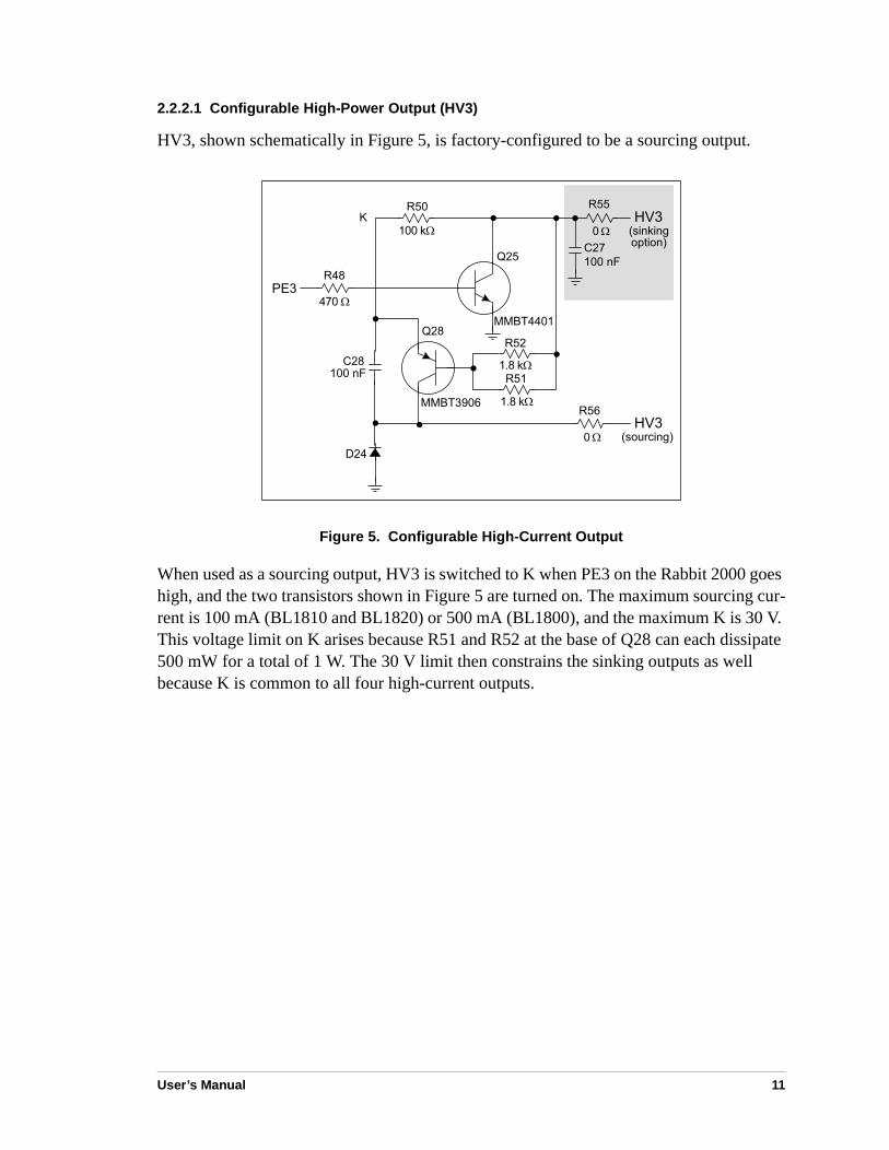
2.2.2.1 Configurable High-Power Output (HV3)
HV3, shown schematically in Figure 5, is factory-configured to be a sourcing output.
Figure 5. Configurable High-Current Output
When used as a sourcing output, HV3 is switched to K when PE3 on the Rabbit 2000 goes high, and the two transistors shown in Figure 5 are turned on. The maximum sourcing cur-rent is 100 mA (BL1810 and BL1820) or 500 mA (BL1800), and the maximum K is 30 V. This voltage limit on K arises because R51 and R52 at the base of Q28 can each dissipate 500 mW for a total of 1 W. The 30 V limit then constrains the sinking outputs as well because K is common to all four high-current outputs.
,(.
/
0
1,-
0
,
,-
1,-
,
23'4#%!(56
, 23!(-!(5
'7&!'(6
,(.
User’s Manual 11
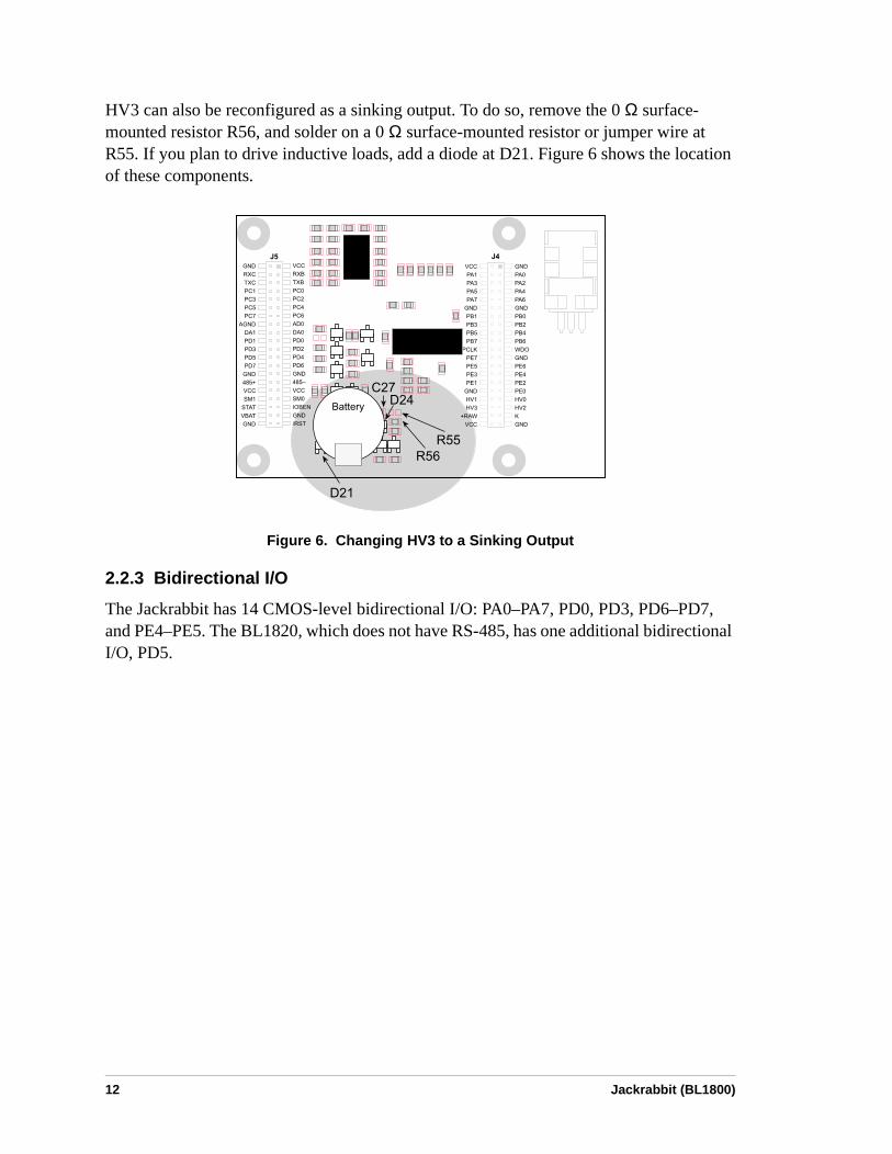
HV3 can also be reconfigured as a sinking output. To do so, remove the 0 Ω surface-mounted resistor R56, and solder on a 0 Ω surface-mounted resistor or jumper wire at R55. If you plan to drive inductive loads, add a diode at D21. Figure 6 shows the location of these components.
Figure 6. Changing HV3 to a Sinking Output
2.2.3 Bidirectional I/O
The Jackrabbit has 14 CMOS-level bidirectional I/O: PA0–PA7, PD0, PD3, PD6–PD7, and PE4–PE5. The BL1820, which does not have RS-485, has one additional bidirectional I/O, PD5.
(
(
)&&$#8
12 Jackrabbit (BL1800)

2.3 A/D Converter
The analog-to-digital (A/D) converter, shown in Figure 7, compares the DA0 voltage to AD0, the voltage presented to the converter. DA0 therefore cannot be used for the digital-to-analog (D/A) converter when the A/D converter is being used.
Figure 7. Schematic Diagram of A/D Converter
The A/D converter transforms the voltage at DA0 into a 20 mV window centered around DA0. For example, if DA0 is 2.0 V, the window in the A/D converter would be 1.990 V to 2.010 V. If AD0 > 2.010 V, PE7 would read high and PE6 would read low. If 1.990 V < AD0 < 2.010 V, PE7 would read low and PE6 would read low. This is the case when the A/D input is exactly the same as DA0. If AD0 < 1.990 V, PE7 would read low and PE6 would read high.
PE6 can be imagined to be a “DA0 voltage is too high” indicator. If DA0 is larger than the analog voltage presented at AD0, then PE6 will be true (high). If this happens, the pro-gram will need to reduce the DA0 voltage.
PE7 can be imagined to be a “DA0 voltage is too low” indicator. If DA0 is smaller than the analog voltage presented at AD0, then PE7 will be true (high). If this happens, the pro-gram will need to raise the DA0 voltage.
The A/D input, AD0, is the same as DA0 only when PE6 and PE7 are low. Because the A/D converter circuit uses a 20 mV window, the accuracy is ±10 mV. DA0 can range from 0.1 V to 2.8 V, which represents 270 steps of ±10 mV. This is better than 8-bit accuracy. Since the D/A converter is able to change the DA0 output in 3.88 mV steps, there are 697 steps over the range from 0.1 V to 2.8 V. This represents a resolution of more than 9 bits.
–
+
–
+
%% %%
,-
1,-
,
,
1,-
/
,
,
,&'',9!59
,&'',*':
User’s Manual 13

There is a 10 kΩ resistor, R31, connected between Vcc and AD0. This resistor should pro-vide an appropriate voltage divider bias for a variety of common thermistors so that they can be connected directly between AD0 and ground. The A/D converter load is the 10 kΩ resistor connected to Vcc. Remove R31 if a smaller load is desired—this will lead to a very high input impedance for the A/D converter.
The A/D converter has no reference voltage. There is a relative accuracy between mea-surements, but no absolute accuracy. This is because Vcc can vary ±5%, the pulse-width modulated outputs might not reach the full 0 V and 5 V rails out of the Rabbit 2000 micro-processor, and the gain resistors used in the circuit have a 1% tolerance. For these reasons, each Jackrabbit needs to be calibrated individually, with the constants held in software, to be able to rely on an absolute accuracy. The Jackrabbit is sold without this calibration sup-port.
The algorithm provided to perform the conversion does a successive approximation search for the analog voltage. This takes an average of 150 ms, and a maximum of 165 ms, with a 14.7 MHz Jackrabbit.
14 Jackrabbit (BL1800)

2.4 D/A Converters
Two digital-to-analog (D/A) converter outputs, DA0 and DA1, are supplied on the Jack-rabbit. These are shown in Figure 8.
The D/A converters have no reference voltage. Although they may be fairly accurate from one programmed voltage to the next, they do not have absolute accuracy. This is because Vcc can change ±5%, the PWM outputs might not achieve the full 0 V and 5 V rail out of the processor, and the gain resistors in the circuit have a 1% tolerance. The D/A converters therefore need individual calibration, with the calibration constants held in software before absolute accuracy can be relied on. The Jackrabbit is sold without such calibration.
Figure 8. Schematic Diagram of D/A Converters
Note that DA0 is used to provide a reference voltage for the A/D converter and is unavail-able for D/A conversion when the A/D converter is being used.
Pulse-width modulation (PWM) is used for the D/A conversion. This means that the digi-tal signal, which is either 0 V or 5 V, is a train of pulses. This means that if the signal is taken to be usually at 0 V (or ground), there will be 5 V pulses. The voltage will be 0 V for a given time, then jump to 5 V for a given time, then back to ground for a given time, then back to 5 V, and so on. A hardware filter in the circuit consisting of a resistor and capacitor averages the 5 V signal and the 0 V signal over time. Therefore, if the time that the signal is at 5 V is equal to the time the signal is 0 V, the duty cycle will be 50%, and the average signal will be 2.5 V. If the time at 5 V is only 25% of the time, then the average voltage will be 1.25 V. Thus, the software needs to only vary the time the signal is at 5 V with respect to the time the signal is at 0 V to achieve any desired voltage between 0 V and 5 V.
–
+
%%
/,
,-
1,-
1,-
,-
,(.
,-
–
+
1,- ,(.
,-
,-
User’s Manual 15

It is very easy to do pulse-width modulation with the Rabbit 2000 microprocessor because of the chip’s architecture.
2.4.1 DA1
The op amp supporting DA1 converts pulse-width modulated signals to an analog voltage between 0 V and 5 V. A digital signal that varies with time is fed from PD4. The resolution of the DA1 output depends on the smallest increment of time to change the on/off time (the time between 5 V and 0 V). The Jackrabbit uses the Rabbit 2000’s Port D control reg-isters to clock out the signal at a timer timeout. The timer used is timer B. Timer B has 10 bits of resolution so that the voltage can be varied in 1/1024 increments. The resolution is thus about 5 mV (5 V/1024).
R28 is present solely to balance the op amp input current bias. R25 helps to achieve a volt-age close to ground for a 0% duty cycle.
A design constraint dictates how fast timer B must run. The hardware filter has a resistor-capacitor filter that averages the 0 V and 5 V values. Its effect is to smooth out the digital pulse train. It cannot be perfect, and so there will be some ripple in the output voltage. The maximum signal decay between pulses will occur when DA1 is set to 2.5 V. This means the pulse train will have a 50% duty cycle. The maximum signal decay will be
where RC = 0.01 s for 14.7 MHz Jackrabbits, and t is the pulse on or off time (not the length of the total cycle).
Timer B is driven at the Rabbit 2000 frequency divided by 2. The frequency achievable with a 14.7 MHz clock is (14.7 MHz/2)/1024 = 7.17 kHz. This is a period of 1/f = 139 µs. For a 50% duty cycle, half of the period will be high (70 µs at 5 V), and half will be low (70 µs at 0 V). Thus, a 14.7 MHz Jackrabbit has t = 70 µs. Based on the standard capacitor discharge formula, this means that the maximum voltage change will be
This is less than a 20 mV peak-to-peak ripple.
The DA1 output can be less than 100 mV for a 0% duty cycle and above 3.5 V for a 100% duty cycle. Because of software limitations on the low side and hardware limitations on the high side, the duty cycle can only be programmed from 12% to 72%. The low limita-tion allows the software to perform other tasks as well as maintain the PWM for the D/A converters. The high limitation is simply the maximum voltage obtainable with the LM324 op amp used in the circuit. Anything outside the 12%–72% range gets output as
2.5 V 1 e
t–RC--------
–×
2.5 V 1 e
70 µs–0.01 s----------------
–× 17.4 mV=
16 Jackrabbit (BL1800)

either a 0% or a 100% duty cycle. The duty cycle is programmed as the high-time count of 1024 total counts of the Rabbit 2000’s timer B. Thus, 256 counts would be 25% of 1024 counts, and corresponds to a 25% duty cycle.
Table 2 lists typical DA1 voltages measured for various duty cycle values with a load larger than 1 MΩ.
It is important to remember that the DA1 output voltage will not be realized instanta-neously after programming in a value. There is a settling time because of the RC time con-stant (R24 × C22), which is 10 ms. For example, the voltage at any given time is
V = VP – (VP – VDA1)e(-t/RC) (EQ 1)
where V is the voltage at time t, VP is the programmed voltage, VDA1 is the last DA1 out-put voltage from the D/A converter, and RC is the time constant (10 ms). The settling will be within 99.326% (or within about 21 mV for a 3 V change in voltage) after five time constants, or 50 ms. Six time constants, 60 ms, will allow settling to within 99.75% (or to within about 8 mV for a 3 V change in voltage). Seven time constants, 70 ms, will allow settling to within 99.91% (or to within about 3 mV for a 3 V change in voltage).
An LM324 op amp, which can comfortably source 10 mA throughout the D/A converter range, drives the D/A converter output. If the output voltage is above 1 V, the D/A con-verter can comfortably sink 10 mA. Below 1 V, the D/A converter can only sink a maxi-mum of 100 µA.
To summarize, DA1 is provided uncalibrated, can be programmed with a resolution of 5 mV and a peak-to-peak ripple less than 20 mV over the range from 0.7 V to 3.5 V and 0 V. The settling time to within 21 mV is 50 ms.
Table 2. Typical DA1 Voltages for Various Duty Cycles
Duty Cycle(%)
Voltage(V)
Programmed Count
0 0.002 0–122
12 0.620 123
25 1.242 256
50 2.483 512
72 3.567 742
100 3.567 743–1024
User’s Manual 17

2.4.2 DA0
The op amp supporting DA0 translates a 12%–88% duty cycle to an analog voltage range of 0 V to 3 V. The software operates only within this duty cycle; a duty cycle less than 12% is rounded down to 0%, and any duty cycle above 88% is rounded up to 100%.
DA0 uses a voltage divider that consists of R21 and R27 and a gain-offset circuit that con-sists of R26 and R29 to achieve the output range of 0 V to 3 V within the software duty cycle.
The DA0 output can be less than 100 mV for a 0% duty cycle and above 3.0 V for a 100% duty cycle. The duty cycle is programmed as the high-time count of 1024 total counts of the Rabbit 2000’s timer B. Thus, 256 counts would be 25% of 1024 counts, and corre-sponds to a 25% duty cycle.
Table 3 lists typical DA0 voltages measured for various duty cycle values with a load larger than 1 MΩ.
It is important to remember that the DA0 output voltage will not be realized instantaneously after programming in a value. There is a settling time because of the RC time constant (R21 || R27 × C20), which is 7.68 ms. For example, the voltage at any given time is
V = VP – (VP – VDA0)e(-t/RC) (EQ 2)
where V is the voltage at time t, VP is the programmed voltage, VDA0 is the last DA0 out-put voltage from the D/A converter, and RC is the time constant (7.68 ms). The settling will be within 99.326% (or within about 21 mV for a 3 V change in voltage) after five time constants, or 38 ms. Six time constants, 46 ms, will allow settling to within 99.75% (or to within about 8 mV for a 3 V change in voltage). Seven time constants, 54 ms, will allow settling to within 99.91% (or to within about 3 mV for a 3 V change in voltage).
The settling time is reduced somewhat by precharging capacitor C20 with pulse-width modulation from PD2.
Table 3. Typical DA0 Voltages for Various Duty Cycles
Duty Cycle(%)
Voltage(V)
Programmed Count
0 0.074 0–122
12 0.076 123
25 0.530 256
50 1.467 512
75 2.406 768
88 2.875 901
100 3.345 902–1024
18 Jackrabbit (BL1800)

The resolution of the DA0 output depends on the smallest increment of time to change the on/off time (the time between 5 V and 0 V). The Jackrabbit uses the Rabbit 2000’s Port D control registers to clock out the signal at a timer timeout. The timer used is timer B. Timer B has 10 bits of resolution so that the voltage can be varied in 1/1024 increments. The resolution is thus about 3.88 mV for the DA0 output voltage range of 0 V to 3 V in the 12%–88% duty cycle.
An LM324 op amp, which can comfortably source 10 mA throughout the D/A converter range, drives the D/A converter output. If the output voltage is above 1 V, the D/A con-verter can comfortably sink 10 mA. Below 1 V, the D/A converter can only sink a maxi-mum of 100 µA.
The peak-to-peak ripple on DA0 is less than 3 mV. There is a way to get rid of the ripple for very small periods of time. To do that, simply program the PWM port from a PWM output to a high-impedance input. This will allow the capacitor to hold the voltage subject only to leakage currents, which add up to about 1 µA. This will cause the capacitor to change voltage at the rate of 10 V per second, or 10 mV per millisecond. Practically, this means that the PWM can stop for about 1 ms (seven 1024-count D/A converter cycles on a 14.7 MHz processor clock) with a voltage movement of less than 10 mV.
To summarize, DA0 is provided uncalibrated, can be programmed with a resolution of 3.88 mV and a peak-to-peak ripple less than 3 mV over the range from 0.1 V to 2.8 V and at 3.35 V. The settling time to within 3 mV is 54 ms.
User’s Manual 19

2.5 Serial Communication
The Jackrabbit has two RS-232 (3-wire) serial channels, one RS-485 serial channel, and one synchronous CMOS serial channel.
2.5.1 RS-232
The Jackrabbit’s two RS-232 serial channels are connected to an RS-232 transceiver, U4, an industry-standard MAX232 chip. U4 provides the voltage output, slew rate, and input voltage immunity required to meet the RS-232 serial communication protocol. Basically, the chip translates the Rabbit 2000’s 0 V to +Vcc signals to ±10 V. Note that the polarity is reversed in an RS-232 circuit so that +5 V is output as –10 V and 0 V is output as +10 V. U4 also provides the proper line loading for reliable communication.
The Rabbit 2000 serial port B signals are presented as RS-232 compliant signals TXB (serial port B transmit) and RXB (serial port B receive) on header J5.
The Rabbit 2000 serial port C signals are presented as RS-232 compliant signals TXC (serial port C transmit) and RXC (serial port C receive) on header J5.
The maximum baud rate for each RS-232 serial channel is 115,200 bps. RS-232 can be used effectively at this baud rate for distances up to 15 m.
Because two RS-232 transmit and two RS-232 receive lines are available, one serial chan-nel can be used for serial transmit and receive, and the other serial channel can be used as a general digital I/O for RTS/CTS handshaking. Although the present release of Dynamic C does not support RTS/CTS handshaking in its libraries, it is possible to write your own software.
2.5.2 RS-485
The Jackrabbit has one RS-485 serial channel, which is connected to the Rabbit 2000 serial port D through U6, an RS-485 transceiver. U6 supports the RS-485 serial communica-tion protocol. The chip’s slew rate limiters provide for a maximum baud rate of 250,000 bps. The half-duplex communication uses the Rabbit 2000’s PD5 pin to control the data enable on the communication line.
The Jackrabbit can be used in an RS-485 multidrop network. Connect the RS-485+ to RS-485+ and RS-485– to RS-485– using single twisted-pair wires (nonstranded, tinned) as shown in Figure 9.
20 Jackrabbit (BL1800)

Figure 9. Multidrop Jackrabbit Network
0
; <+'#*"=,(%1
(
01
0
0
(
0
((
(
>
)??!&,
+
+
0
; <+'#*"=,(%1
(
01
0
0
(
0
((
(
>
)??!&,
+
+
0
; <+'#*"=,(%1
(
01
0
0
(
0
((
(
>
)??!&,
+
+
#'4(",#$%'@@$("$"
User’s Manual 21

The Jackrabbit comes with a 220 Ω termination resistor and 681 Ω bias resistors already installed, as shown in Figure 10.
Figure 10. RS-485 Termination and Bias Resistors
The load these bias and termination resistors present to the RS-485 transceiver (U6) limits the number of Jackrabbits in a multidrop network to one master and nine slaves, unless the bias and termination resistors are removed. When using more than 10 Jackrabbits in a multidrop network, leave the 681 Ω bias resistors in place on the master Jackrabbit, and leave the 220 Ω termination resistors in place on the Jackrabbit at each end of the network.
2.5.3 Programming Port
The Jackrabbit has a 10-pin program header labeled J3. The programming port uses the Rabbit 2000’s serial port A for communication. The Rabbit 2000 startup-mode pins (SMODE0, SMODE1) are presented to the programming port so that an externally con-nected device can force the Jackrabbit to start up in an external bootstrap mode.
The programming port is used to start the Jackrabbit in a mode where the Jackrabbit will download a program from the port and then execute the program. The programming port transmits information to and from a PC while a program is being debugged.
The Jackrabbit can be reset from the programming port.
The Rabbit 2000 status pin is also presented to the programming port. The status pin is an output that can be used to send a general digital signal.
The clock line for serial port A is presented to the programming port, which makes fast serial communication possible.
A
,
,
,
0
; <+'#*"=,(%1
(
01
0
0
(
0
((
(
>
)??!&,
+
+
22 Jackrabbit (BL1800)

2.6 Memory
2.6.1 SRAM
The Jackrabbit is designed to accept 32K to 512K of SRAM packaged in an SOIC case.
Standard Jackrabbit models come with 128K of SRAM. A factory-installed option for 512K of SRAM is available. Figure 11 shows the locations and the jumper settings for the jump-ers at JP1 used to set the SRAM size. The “jumpers” are 0 Ω surface-mounted resistors.
Figure 11. Jackrabbit Jumper Settings for SRAM Size
NOTE: For ordering or other information involving the factory-intsalled 512K SRAM option, call your Z-World Sales Representative at (530)757-3737.
No 0 Ω surface-mounted resistors are installed at JP1 for 32K SRAM.
2.6.2 Flash EPROM
The Jackrabbit is also designed to accept 128K to 512K of flash EPROM packaged in a TSOP case.
NOTE: Z-World recommends that any customer applications should not be constrained by the sector size of the flash memory since it may be necessary to change the sector size in the future.
A Flash Memory Bank Select jumper configuration option exists at JP3 with 0 Ω surface-mounted resistors for Jackrabbit boards labeled 175-0255. This option, used in conjunc-tion with some configuration macros, allows Dynamic C to compile two different co-resi-dent programs for the upper and lower halves of the 256K flash in such a way that both programs start at logical address 0000. This is useful for applications that require a resi-dent download manager and a separate downloaded program. See Technical Note 218, Implementing a Serial Download Manager for a 256K Flash, for details.
0
(
(
"
(
; <+'#*"=,(%1
(
01
0
0
(
0
((
(
>
+
+
User’s Manual 23
2.7 Other Hardware
2.7.1 External Interrupts
Jackrabbit boards that carry the CE mark have external interrupts available on digital inputs PE4 and PE5.
2.7.2 Clock Doubler
Jackrabbit BL1810 and BL1820 models take advantage of the Rabbit 2000 microproces-sor’s internal clock doubler. A built-in clock doubler allows half-frequency crystals to be used to reduce radiated emissions. The 14.7 MHz frequency is generated using a 7.37 MHz resonator. The clock doubler is disabled automatically in the BIOS for crystals or resonators with a frequency above 12.9 MHz.
The clock doubler may be disabled if 14.7 MHz clock speeds are not required. Disabling the Rabbit 2000 microprocessor’s internal clock doubler will reduce power consumption and further reduce radiated emissions. The clock doubler is disabled with a simple change to the BIOS as described below.
1. Open the BIOS source code file, RABBITBIOS.C in the BIOS directory.
2. Change the line
#define CLOCK_DOUBLED 1 // set to 1 to double clock if // Rabbit 2000: crystal <= 12.9024 MHz, // Rabbit 3000: crystal <= 26.7264 MHz, // or to 0 to always disable clock doubler
to read as follows.
#define CLOCK_DOUBLED 0
3. Save the change using File > Save.
24 Jackrabbit (BL1800)

2.7.3 Spectrum Spreader
Jackrabbit boards that carry the CE mark have a Rabbit 2000 microprocessor that features a spectrum spreader, which helps to mitigate EMI problems. By default, the spectrum spreader is on automatically for Jackrabbit BL1810 and BL1820 boards that carry the CE mark when used with Dynamic C 7.32 or later versions, but the spectrum spreader may also be turned off or set to a stronger setting. The means for doing so is through a simple change to the following BIOS line in a way that is similar to the clock doubler described above.
#define ENABLE_SPREADER 1 // Set to 0 to disable spectrum spreader // 1 to enable normal spreading, or // 2 to enable strong spreading.
NOTE: The spectrum spreader is off by default for Jackrabbit BL1800 models, and needs to be enabled for them to be CE-compliant. To allow the flash memory and RAM chips to accomodate the occasional higher frequencies associated with the spectrum spreader being turned on for the Jackrabbit BL1800 models only, you will need at least one wait state for both the flash memory and the RAM. The strong spectrum-spreading setting is not needed for any Jackrabbit board.
The number of wait states is specified in the following code from the LIB\BOARDTYPES library. (There are 0 wait states by default.)
#ifndef NUM_RAM_WAITST#define NUM_RAM_WAITST 0#endif#ifndef NUM_FLASH_WAITST#define NUM_FLASH_WAITST 0#endif
There is no spectrum spreader functionality for Jackrabbit boards that do not carry the CE mark or when using any Jackrabbit with a version of Dynamic C prior to 7.30.
User’s Manual 25

26 Jackrabbit (BL1800)

APPENDIX A. SPECIFICATIONS
Appendix A provides the specifications for the Jackrabbit.
User’s Manual 27

A.1 Electrical and Mechanical Specifications
Figure A-1 shows the mechanical dimensions for the Jackrabbit.
Figure A-1. Jackrabbit (BL1810) Dimensions
Table A-1 provides the pin 1 locations for the Jackrabbit headers.
Table A-1. Jackrabbit Header Pin 1 Locations
Header DescriptionPin 1 (x,y)
Coordinates
J1 Power supply input (0.110, 0.700)
J2 External battery (0.415, 0.638)
J3 Programming port (0.145, 0.149)
J4 Jackrabbit subsystems (0.984, 2.023)
J5 Jackrabbit subsystems (3.184, 2.023)
126
1/26
1
216
1
261
26
1,"!)=,B26
12/6
126
1
26
1/
26
1/
26
1
26
1/
26
1/
26
12/6
28 Jackrabbit (BL1800)

Table A-2 lists the electrical, mechanical, and environmental specifications for the Jackrabbit boards.
Table A-2. Jackrabbit Board Specifications
Parameter BL1800 BL1810 BL1820
Microprocessor Rabbit 2000 @ 29.5 MHz Rabbit 2000 @ 14.7 MHz
Flash EPROM256K
(supports 128K–512K)128K
(supports 128K–512K)
SRAM128K
(supports 32K–512K)
Backup Battery3 V lithium coin type, 950 mA·h,
supports real-time clock and SRAMNone
Digital Inputs 6, CMOS-level 7, CMOS-level
Digital Outputs
4 CMOS-level plus4 high-power outputs—3 sink up to 1 A and 30 V each, 1 sources up to 500 mA
4 CMOS-level plus4 high-power outputs—3 sink up to 200 mA and 30 V each, 1 sources up to 100 mA
5 CMOS-level plus4 high-power outputs—3 sink up to 200 mA and 30 V each, 1 sources up to 100 mA
Configurable I/O 14 CMOS-level: 8 are bytewide, 6 are by bit15 CMOS-level:
8 are bytewide, 7 are by bit
Analog InputsOne low-grade A/D input—input range 0.1 V to 2.8 V,
9-bit resolution, 8-bit accuracy, 10 samples/s
Analog OutputsTwo 9-bit filtered and buffered PWM outputs,
one 0.1–2.8 V DC, one 0.7–3.5 V DC, update rate 50 Hz
Serial Ports
Up to four serial ports:
• two RS-232 or one RS-232 (with CTS/RTS) rated at 15 kV ESD
• one RS-485 rated at 15 kV ESD (RS-485 driver not installed on BL1820)
• one 5 V CMOS-compatible programming port
Two serial ports (A and B) can be clocked.
Serial RateMax. burst rate = CLK/32 (async)
Max. sustained rate = CLK/64
Connectors Two 2 × 20, 2 mm IDC headers
Real-Time Clock Yes
TimersFive 8-bit timers (four cascadable from the first)
and one 10-bit timer with two match registers
Watchdog/Supervisor Yes
Power8–40 V DC, 1.2 W max.,
switching regulator7.5–25 V DC, 100 mA, linear regulator
Operating Temperature –40°C to +70°C
Humidity 5% to 95%, noncondensing
Board Size2.50" × 3.50" × 0.76"
(64 mm × 89 mm × 19 mm)2.50" × 3.50" × 0.94"
(64 mm × 89 mm × 24 mm)2.50" × 3.50" × 0.63"
(64 mm × 89 mm × 16 mm)
User’s Manual 29

A.2 Jumper Configurations
Figure A-2 shows the header and jumper locations used to configure the various Jackrabbit options.
Figure A-2. Location of Jackrabbit Configurable Positions
;
;
<+'#*"=,(%1;
;
#$%
&$%
)&&$#8
30 Jackrabbit (BL1800)

Table A-3 lists the configuration options. 0 Ω surface mount resistors are used for all the header positions.
NOTE: Header JP3 is available only on Jackrabbit boards labeled 175-0255. These boards were introduced in 2003.
Table A-3. Jackrabbit Jumper Configurations
Header Description Pins ConnectedFactory Default
JP1 SRAM Size
n.c. 32K
1–2 128K ×2–3 512K
JP2 Flash Memory Size1–2 128K/256K ×2–3 512K
JP3 Flash Memory Bank Select1–2 Normal Mode ×2–3 Bank Mode
— HV3 Sinking/Sourcing
D21R55
Sinking
R56 Sourcing ×
—RS-485 Bias and Termination Resistors (not isnatlled on BL1820)
R17 Termination resistor ×R16R18
Bias resistors ×
User’s Manual 31

A.3 Conformal Coating
The areas around the crystal oscillator and the battery backup circuit on the Jackrabbit have had the Dow Corning silicone-based 1-2620 conformal coating applied. The confor-mally coated areas are shown in Figure A-3. The conformal coating protects these high-impedance circuits from the effects of moisture and contaminants over time, and helps to maintain the accuracy of the real-time clock.
Figure A-3. Jackrabbit Areas Receiving Conformal Coating
Any components in the conformally coated area may be replaced using standard soldering procedures for surface-mounted components. A new conformal coating should then be applied to offer continuing protection against the effects of moisture and contaminants.
NOTE: For more information on conformal coatings, refer to Technical Note 303, Conformal Coatings.
'(C'#@)**8,%')&$",)#$)
32 Jackrabbit (BL1800)
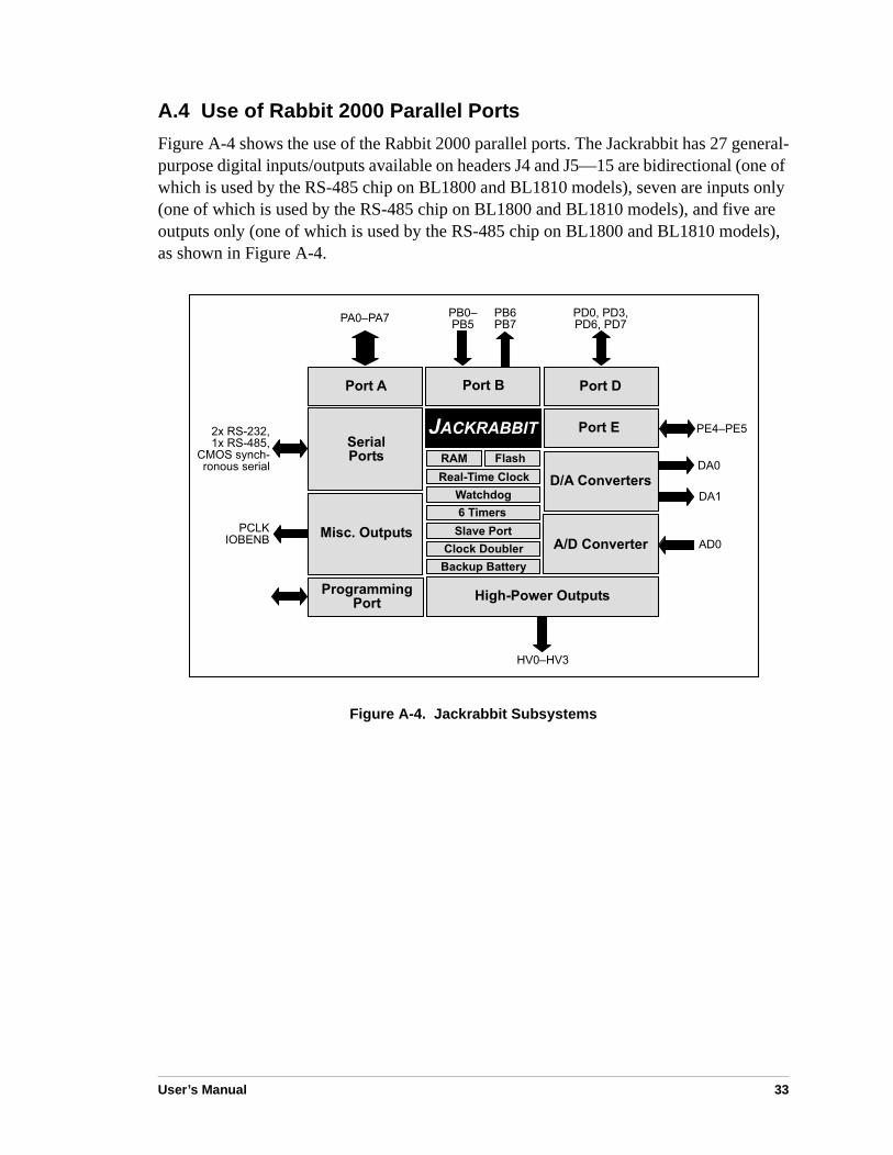
A.4 Use of Rabbit 2000 Parallel Ports
Figure A-4 shows the use of the Rabbit 2000 parallel ports. The Jackrabbit has 27 general-purpose digital inputs/outputs available on headers J4 and J5—15 are bidirectional (one of which is used by the RS-485 chip on BL1800 and BL1810 models), seven are inputs only (one of which is used by the RS-485 chip on BL1800 and BL1810 models), and five are outputs only (one of which is used by the RS-485 chip on BL1800 and BL1810 models), as shown in Figure A-4.
Figure A-4. Jackrabbit Subsystems
'
! !2 !
!, !!
!!""#!
B,+=B,+=
,38(%9+#'('43,3$#!)*
=,==,
34
15" !
22 !6
&) !
' !
5" &
%&#' ! !
!
%&#' ! !
7
User’s Manual 33

The ports on the Rabbit 2000 microprocessor used in the Jackrabbit are configurable, and so the factory defaults can be reconfigured. Table A-4 lists the Rabbit 2000 factory defaults and the alternate configurations.
Table A-4. Jackrabbit Pinout Configrations
PinRabbit 2000
Factory DefaultAlternate Use Jackrabbit Use
PA0–PA7
Parallel I/OSlave port data bus SD0–SD7
PB0 Input Serial port clock CLKB PB1 (CLKA) is connected to J3 (programming port)
PB1 Input Serial port clock CLKA
PB2 Input Slave port write /SWR
PB3 Input Slave port read /SRD
PB4 Input Slave port address lines SA1–SA0PB5 Input
PB6 Output
PB7 OutputSlave port attention line /SLAVEATTN
PC0 Output TXDConnected to RS-485 IC Tx input
PC1 Input RXDConnected to RS-485 IC Rx output
PC2 Output TXCConnected to RS-232 IC Tx input
PC3 Input RXCConnected to RS-232 IC Rx output
PC4 Output TXBConnected to RS-232 IC Tx input
PC5 Input RXBConnected to RS-232 IC Rx output
PC6 Output TXA Connected to programming portPC7 Input RXA
34 Jackrabbit (BL1800)

As shown in Table A-4, pins PE4 and PE5 can instead be used as external INT0B and INT1B interrupts. Pins PD6 and PD7 can instead be used to access Serial Port A on the Rabbit 2000 microprocessor. Pins PB0 and PB1 can instead be used to access the clock on Serial Port B and Serial Port A of the Rabbit 2000 microprocessor.
PD0
Bitwise or parallel programmable I/O, can be driven or open-drain output
PD1Connected to control DA0
PD2Connected to control DA0
PD3
PD4 ATXB outputConnected to control DA1
PD5 ARXB inputConnected to RS-485 IC data enable input
PD6 ATXA output
PD7 ARXA input
PE0
Bitwise or parallel programmable I/O
I0 output or INT0A input HV0 output control
PE1 I1 output or INT1A input HV1 output control
PE2 I2 output HV2 output control
PE3 I3 output HV3 output control
PE4I4 output or external INT0B input
PE5I5 output or external INT1B input
PE6 I6 outputConnected to A/D comparator output
PE7I7 output or slave port chip select /SCS
Connected to A/D comparator output
PCLK Peripheral clock Output
IOBEN I/O buffer enable Output
WDO Watchdog output Single low pulse output
STAT Status OutputConnected to programming port
Table A-4. Jackrabbit Pinout Configrations (continued)
PinRabbit 2000
Factory DefaultAlternate Use Jackrabbit Use
User’s Manual 35

The four output-only pins are located on PB6–PB7, PCLK, and IOBEN. PB7 can also be used with the slave port of the Rabbit 2000 microprocessor. The primary function of PCLK is as a peripheral clock or a peripheral clock ÷ 2, but PCLK can instead be used as a digital output. Similarly, IOBENB is an I/O buffer enable, but can instead be used as a digital output. STAT and WDO also have limited uses as digital outputs.
36 Jackrabbit (BL1800)

APPENDIX B. PROTOTYPING BOARD
Appendix B describes the features and accessories of the Proto-typing Board, and explains the use of the Prototyping Board todemonstrate the Jackrabbit and to build prototypes of your owncircuits.
User’s Manual 37

B.1 Mechanical Dimensions and Layout
Figure B-1 shows the mechanical dimensions and layout for the Jackrabbit Prototyping Board.
Figure B-1. Jackrabbit Prototyping Board
;
;
;
;
<
2+6
26
;
11
11
+
/
;
Buzzer
#$%
&$%
;
;
;
;
;
;
; ;
/
; ,>,
/
;
<
26
2+6
11
11
<+'#*"=,(%1
+
126
1
26
38 Jackrabbit (BL1800)

B.2 Using the Prototyping Board
The Prototyping Board is actually both a demonstration board and a prototyping board. As a demonstration board, it can be used to demonstrate the functionality of the Jackrabbit right out of the box without any modifications to either board. There are no jumpers or dip switches to configure or misconfigure on the Prototyping Board so that the initial setup is very straightforward.
Once you have looked at the basic sample programs described in the Jackrabbit (BL1800) Getting Started Manual, solder the headers included in the bag of spare parts onto the Prototyping Board. Solder a 10-pin header to the top side at location J1. Solder the addi-tional headers shown in Figure B-2 onto the bottom side.
Figure B-2. Where to Solder Additional Headers
;
;
;
;
<
2+6
26
;
11
11
+
/
;
Buzzer
'
'
'
#$%
&$%
;
;
;
;
;
;
; ;
/
; ,>,
/
;
<
26
2+6
11
11
<+'#*"=,(%1
+
'(
2('&,!(%*4"$"!(,$D$*'7@$(&,!&6
User’s Manual 39

B.2.1 Demonstration Board
A relay, a thermistor, four additional LEDs, and a serial cable are included in a bag of parts to further allow exploration of the Jackrabbit‘s operation.
The SPDT relay handles 120 V at 5 A with a 12 V activating coil. The layout to accept this relay is included on the top side of the Prototyping Board. Note that the relay coil connec-tions need to be wired to one of the sinking high-power outputs (HV0–HV2) of the Jackrabbit. Install the relay on the bottom side of the Prototyping Board, as shown in Figure B-3.
Figure B-3. Installation of Relay on Prototyping Board
NOTE: COIL(+) must be connected to a 12 V power supply when using the relay. This is the nominal voltage supplied as +RAW when the transformer supplied with the Development Kit is used, and in this case you may connect COIL(+) to +RAW. If you use another power supply, connect COIL(+) to +12 V if +RAW is different.
NOTE: If you do use the transformer supplied with the Development Kit for COIL(+), be aware that its voltage may be as high as 16 V at low current draws. This needs to be taken into consideration if you plan to use a 12 V relay in critical applications.
6&#E1F,2,@@6,37)%!(5G
E&$89:;,)(",&$89;,37)%!(5!3,1F,21,@@6G
;
;
;
;
<
2+6
26
;
11
11
+
/
;
&$%
)* +,
:<,,&$89:; <=,,&$89;>,,:3
40 Jackrabbit (BL1800)

The thermistor has a nominal room-temperature resistance of about 10 kΩ, which drops to about 6 kΩ at 40°C. Once you solder the thermistor onto the RT1 pads (see Figure B-4) on the Prototyping Board, the A/D readings on AD0 will change with temperature.
If the 10 kΩ potentiometer is removed, the A/D change with temperature will be larger.
The LEDs can be mounted in positions DS5–DS8, shown in Figure B-5, to display the complete status for Parallel Port A.
The serial cable included in the parts bag can be used to connect the Jackrabbit’s RS-232 outputs from header J1 on the Prototyping Board to an available DE9 PC serial port.
Unlike the CMOS-level signals on header J3, the programming port on the Jackrabbit board, the sig-nals on header J1 on the Prototyping Board are full RS-232 level signals without needing the CMOS to RS-232 converter that is present in the program-ming cable. The RS-232 level signals are processed via the MAX232 transceiver chip, U4, on the Jack-rabbit board to Serial Ports B and C of the Rabbit 2000. The CMOS-level signals on the program-ming port are connected to Serial Port A.
Figure B-4. Thermistor and Potentiometer Locations
Figure B-5. LED Location
9$#@!3&'#
,-'&$(&!'@$&$#
;
<
2+6
H -.$/$0-1/
H%%12$-1/
/
User’s Manual 41

B.2.2 Prototyping Board
To maximize the availability of Jackrabbit resources, the demonstration hardware (LEDs, switches, potentiometer, buzzer) on the Prototyping Board may be disconnected. This is done by cutting the traces seen between and within the silk-screen outline of headers JP1 and JP2 on the Prototyping Board. Figure B-6 shows the 16 places where cuts should be
made. An exacto knife or high-speed precision grinder tool like a Dremel® tool would work nicely to cut the traces. Alternatively, if safety is a major concern, a small standard screwdriver may be carefully and forcefully used to wipe through the PCB traces.
Figure B-6. Where to Cut Traces to Permanently Disable Demonstration Hardware on Prototyping Board
Jumpers across the appropriate pins on headers JP1 and JP2 can be used to reconnect spe-cific demonstration hardware later if needed. Each pin is labeled on the PCB to facilitate placing the jumpers. The jumper positions are summarized in Table B-1.
Table B-1. Prototyping Board Jumper Settings
Header JP1 Header JP2 (continued)
Pins Description Pins Description
1–2 Buzzer 5–6 PA2 to LED DS3
3–5 K to +5 V 7–8 PA3 to LED DS4
5–6 K to +RAW 9–10 PA4 to LED DS5
7–8 Potentiometer or Thermistor 11–12 PA5 to LED DS6
9–10 Interrupt Enable 13–14 PA6 to LED DS7
Header JP2 15–16 PA7 to LED DS8
Pins Description 17–18 PB2 to switch S1
1–2 PA0 to LED DS1 19–20 PB3 to switch S2
3–4 PA1 to LED DS2 21–22 PB4 to switch S3
4&4&
4&
4&
#$%
;
;
; ;
<
26
2+6
42 Jackrabbit (BL1800)
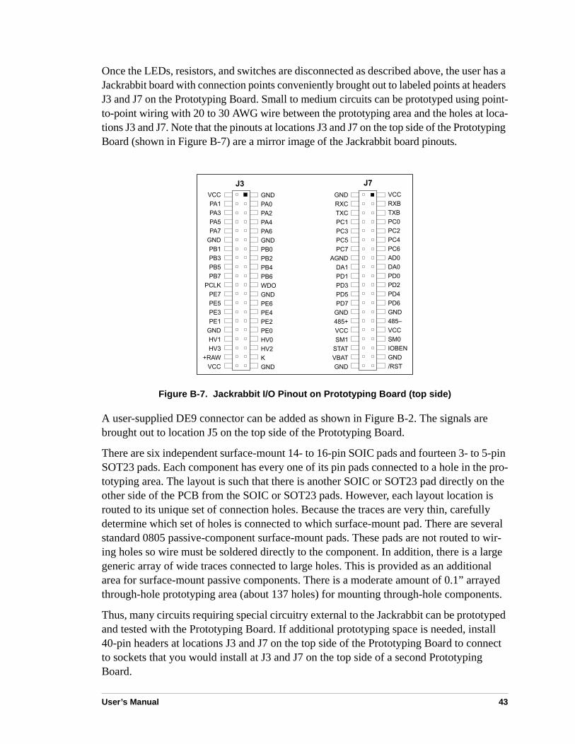
Once the LEDs, resistors, and switches are disconnected as described above, the user has a Jackrabbit board with connection points conveniently brought out to labeled points at headers J3 and J7 on the Prototyping Board. Small to medium circuits can be prototyped using point-to-point wiring with 20 to 30 AWG wire between the prototyping area and the holes at loca-tions J3 and J7. Note that the pinouts at locations J3 and J7 on the top side of the Prototyping Board (shown in Figure B-7) are a mirror image of the Jackrabbit board pinouts.
Figure B-7. Jackrabbit I/O Pinout on Prototyping Board (top side)
A user-supplied DE9 connector can be added as shown in Figure B-2. The signals are brought out to location J5 on the top side of the Prototyping Board.
There are six independent surface-mount 14- to 16-pin SOIC pads and fourteen 3- to 5-pin SOT23 pads. Each component has every one of its pin pads connected to a hole in the pro-totyping area. The layout is such that there is another SOIC or SOT23 pad directly on the other side of the PCB from the SOIC or SOT23 pads. However, each layout location is routed to its unique set of connection holes. Because the traces are very thin, carefully determine which set of holes is connected to which surface-mount pad. There are several standard 0805 passive-component surface-mount pads. These pads are not routed to wir-ing holes so wire must be soldered directly to the component. In addition, there is a large generic array of wide traces connected to large holes. This is provided as an additional area for surface-mount passive components. There is a moderate amount of 0.1” arrayed through-hole prototyping area (about 137 holes) for mounting through-hole components.
Thus, many circuits requiring special circuitry external to the Jackrabbit can be prototyped and tested with the Prototyping Board. If additional prototyping space is needed, install 40-pin headers at locations J3 and J7 on the top side of the Prototyping Board to connect to sockets that you would install at J3 and J7 on the top side of a second Prototyping Board.
)$ %
$
User’s Manual 43

44 Jackrabbit (BL1800)

APPENDIX C. POWER MANAGEMENT
C.1 Power Supplies
Power is supplied to the Jackrabbit board from an external source through either header J1 or header J4. J1 is a 3-pin straight header with a pitch of 0.1". Vin is on pin 2 between
ground on pins 1 and 3. The symmetry allows for a 3-pin cable to be connected either way.
The Jackrabbit board itself is protected against reverse polarity by a Shottky diode at D2 as shown in Figure C-1. The Shottky diode has a low forward voltage drop, 0.3 V, which keeps the minimum DCIN required to power the Jackrabbit lower than a normal silicon diode would allow.
Figure C-1. Jackrabbit Power Supply Schematic
The external power, +RAW, is provided to any daughterboard connected to the Jackrabbit via pin 38 of header J4. +RAW is not protected against reversed polarity, such as could happen if the cable was connected to header J1 offset by one pin. This absence of protec-tion is intentional so as to provide the maximum possible voltage to any daughterboard connected to the Jackrabbit.
Capacitor C1 provides surge current protection for the voltage regulator, and allows the external power supply to be located some distance away from the Jackrabbit board. A switching power supply or a linear power supply option is provided, depending on the Jackrabbit model.
,,A >
;
,I. ,(.
,I.
A
A
%%
%%
,I
/
/
,,A >
User’s Manual 45

The linear voltage regulator is simply a fixed-voltage regulator with a ±5% voltage output tolerance as the temperature changes. The regulator has a small heat sink, which increases the maximum external input voltage. Higher external input voltages increase the voltage dropped by the regulator. The Vcc coming out of the regulator is always 5 V.
The power necessarily dissipated by the regulator can be calculated if both the external input voltage and the current drawn by the Jackrabbit board and daughterboards connected to the Jackrabbit board are known. The current provided by the high-power output drivers does not have to be included if a separate power supply is connected to K so that power does not come from Vcc.
The linear regulator maintains its output voltage to within ±5% as long as the heat sink is dissipating less than 2 W. The regulator will operate outside its specifications when the heat sink is dissipating 2 W to 3.3 W. Thermal shutdown turns the regulator off above 3.3 W. Figure C-2 shows the power operating curves.
Figure C-2. 7805 Linear Regulator Power Operating Curve
The Jackrabbit operating at 14.7 MHz with no loading at the outputs typically consumes 105 mA when the programming cable is connected, and 95 mA when the programming cable is not connected. This means that DCIN can safely be from 7.5 V to 25 V. An addi-tional 50 mA is available for a daughterboard, but the voltage regulation would suffer slightly.
4##$(&,2@ 6
,26
1,JJJJJJJJJJ2,,,6
,JJJJJJJJJJ2,,,6
46 Jackrabbit (BL1800)

The switching voltage regulator is used when there is a need for an additional range in the external input voltage or when lower power consumption is desired. The input voltage range is from 8 V to 40 V.
Figure C-3 shows typical power operating curves for both the linear regulator (BL1810 and BL1820) and the switching regulator (BL1800) for a nonloaded Jackrabbit operating at 14.7 MHz with the programming cable connected.
Figure C-3. Typical Jackrabbit Current Consumption
4##$(&,2@ 6
,26
!"##$%&'%()*+
!"#"#$'&,()*+
User’s Manual 47

C.2 Batteries and External Battery Connections
The soldered-in 950 mA·h lithium coin cell provides power to the real-time clock and SRAM when external power is removed from the circuit. This allows the Jackrabbit to continue to keep track of time and preserves the SRAM memory contents.
The drain on the battery is typically less than 20 µA when there is no external power applied. The battery can last more than 5 years:
The drain on the battery is typically less than 4 µA when there external power is applied. The battery can last for its full shelf life:
Since the shelf life of the battery is 10 years, the battery can last for its full shelf life when external power is applied to the Jackrabbit.
Header J2, shown in Figure C-4, allows external access to the battery. This header makes it possible to connect an external 3 V power supply while replacing the soldered-in 3 V lithium coin-type battery. This allows the Jackrabbit SRAM and real-time clock to retain data while the battery is being replaced.
Figure C-4. External Battery Connections at Header J2
Alternatively, header J2 can be used to accommodate an external battery. In this case, be sure to cut out the soldered-in battery on the Jackrabbit to prevent discharging the external battery into a dead battery.
950 mA·h20 µA
------------------------ 5.4 years.=
950 mA·h4 µA
------------------------ 27 years (shelf life = 10 years).=
;
,
48 Jackrabbit (BL1800)

C.2.1 Battery Backup Circuit
Figure C-5 shows the Jackrabbit battery backup circuitry.
Figure C-5. Jackrabbit Battery Backup Circuit
Resistor R12, shown in Figure C-5, is typically not stuffed on the Jackrabbit board. VRAM and Vcc are equal when power is supplied to the Jackrabbit. R13 prevents any cat-astrophic failure of Q1 from allowing unlimited current to enter the soldered-in battery.
Resistors R14 and R15 make up a voltage divider between the battery voltage and the tem-perature-compensation voltage at the anode of diode D80. This voltage divider biases the base of Q1 to about 2.6 V. VBE on Q1 is about 0.55 V. Therefore, VRAM is about 2.05 V.
These voltages vary with temperature. VRAM varies the least because temperature-com-pensation diodes D80–D82 will offset the variation with temperature of Q1 VBE. R80–
R82 may be stuffed instead of the corresponding D80–D82 to provide the optimum tem-perature compensation.
Resistor R10 provides a minimum load to the regulator circuit.
0
,
1,
,
1,-
,
,
,
User’s Manual 49

The battery-backup circuit serves two purposes:
• It reduces the battery voltage to the real-time clock, thereby reducing the current con-sumed by the real-time clock and lengthening the battery life.
• It ensures that current can flow only out of the battery to prevent charging the battery.
C.2.2 Power to VRAM Switch
The VRAM switch, shown in Figure C-6, allows the soldered-in battery to provide power when the external power goes off. The switch provides an isolation between Vcc and the battery when Vcc goes low. This prevents the Vcc line from draining the battery.
Figure C-6. VRAM Switch
Transistor Q23 is needed to provide a very small voltage drop between Vcc and VRAM (<100 mV, typically 10 mV) so that the processor lines powered by Vcc will not have a significantly different voltage than VRAM.
When the Jackrabbit is not resetting (pin 2 on U21 is high), the /RES line will be high. This turns on Q24, causing its collector (pin 3) to go low. This turns on Q23, allowing VRAM to nearly equal Vcc.
When the Jackrabbit is resetting, the /RES line will go low. This turns off Q23 and Q24, providing an isolation between Vcc and VRAM.
The battery backup circuit keeps VRAM from dropping below 2 V.
C.2.3 Reset Generator
The Jackrabbit uses a reset generator, U21, to reset the Rabbit 2000 microprocessor when the voltage drops below the voltage necessary for reliable operation. The Jackrabbit does not have a reset output presented to the headers. The reset generator has a reset input that can be used to force the Jackrabbit to reset. This input is available on headers J3 and J5, and also on pads directly below header J5. The two pads allow a screwdriver to be used to short the pads, forcing a reset.
.0
,-
0/,-
,
50 Jackrabbit (BL1800)

C.3 Chip Select Circuit
Figure C-7 shows a schematic of the chip select circuit.
Figure C-7. Chip Select Circuit
The current drain on the battery in a battery-backed circuit must be kept at a minimum. When the Jackrabbit board is not powered, the battery keeps the SRAM memory contents and the real-time clock (RTC) going. The SRAM has a powerdown mode that greatly reduces power consumption. This powerdown mode is activated by raising the chip select (CS) signal line. Normally the SRAM requires Vcc to operate. However, only 2 V is required for data retention in powerdown mode. Thus, when power is removed from the circuit, the battery voltage needs to be provided to both the SRAM power pin and to the CS signal line. The CS control circuit accomplishes this task for the CS signal line.
In a powered-up condition, the CS control circuit must allow the processor’s chip select signal /CS1 to control the SRAM’s CS signal /CSRAM. So, with power applied, /CSRAM must be the same signal as /CS1, and with power removed, /CSRAM must be held high (but only needs to be battery voltage high). Q20 and Q21 are MOSFET transistors with opposing polarity. They are both turned on when power is applied to the circuit. They allow the CS signal to pass from the processor to the SRAM so that the processor can peri-odically access the SRAM. When power is removed from the circuit, the transistors will turn off and isolate /CSRAM from the processor. The isolated /CSRAM line has a 100 kΩ pullup resistor to VRAM (R37). This pullup resistor keeps /CSRAM at the VRAM voltage level (which under no power condition is the backup battery’s regulated voltage at a little more than 2 V).
0
0
0
/
User’s Manual 51

Transistors Q20 and Q21 are of opposite polarity so that a rail-to-rail voltages can be passed. When the /CS1 voltage is low, Q20 will conduct. When the /CS1 voltage is high, Q21 will conduct. It takes time for the transistors to turn on, creating a propagation delay. This delay is typically very small, about 10 ns to 15ns.
The signal that turns the transistors on is a high on the processor’s reset line, /RES. When the Jackrabbit is not in reset, the reset line will be high, turning on N-channel Q20 and Q22. Q22 is a simple inverter needed to turn on Q21, an P-channel MOSFET. When a reset occurs, the /RES line will go low. This will cause C23 to discharge through R42 and R40. This small delay (about 160 µs) ensures that there is adequate time for the processor to write any last byte pending to the SRAM before the processor puts itself into a reset state. When coming out of reset, CS will be enabled very quickly because D20 conducts to charge capacitor C23.
52 Jackrabbit (BL1800)

APPENDIX D. ALTERNATEUSE OF THE PROGRAMMING PORT
Appendix D provides additional information for the program-ming port in association with the DIAG and PROG connectorson the programming cable. The PROG connector is used onlywhen the programming cable is attached to the programmingconnector (header J3) while a new application is being devel-oped. Otherwise, the DIAG connector on the programming cableallows the programming cable to be used as an RS-232 toCMOS level converter for serial communication, which isappropriate for monitoring or debugging a Jackrabbit systemwhile it is running.
User’s Manual 53

The programming port, which is shown in Figure D-1, can serve as a convenient commu-nications port for field setup or other occasional communication need (for example, as a diagnostic port). If the port is simply to perform a setup function, that is, write setup infor-mation to flash memory, then the single-board computer can be reset through the program-ming port and a cold boot performed to start execution of a special program dedicated to this functionality.
Figure D-1. Programming Port Pin Assignments
When the PROG connector is used, the /RESET line can be asserted by manipulating DTR and the STATUS line can be read as DSR on the serial port. The target can be restarted by pulsing reset and then, after a short delay, sending a special character string at 2400 bps. To simply restart the BIOS, the string 80h, 24h, 80h can be sent. When the BIOS is started, it can tell whether the programming cable is connected because the SMODE1 and SMODE0 pins are sensed as being high.
Alternatively, the DIAG connector can be used to connect the programming port. The /RESET line and the SMODE1 and SMODE0 pins are not connected to this connector. The programming port is then enabled as a diagnostic port by polling the port periodically to see if communication needs to begin or to enable the port and wait for interrupts. The pull-up resistors on RXA and CLKA prevent spurious data reception that might take place if the pins floated.
If the clocked serial mode is used, the serial port can be driven by having two toggling lines that can be driven and one line that can be sensed. This allows a conversation with a device that does not have an asynchronous serial port but that has two output signal lines and one input signal line.
The line TXA (also called PC6) is zero after reset if the cold-boot mode is not enabled. A possible way to detect the presence of a cable on the programming port is for the cable to connect TXA to one of the SMODE pins and then test for the connection by raising PC6 (by configuring it as a general output bit) and reading the SMODE pin after the cold-boot mode has been disabled. The value of the SMODE pin is read from the SPCR register.
/
,,, 2)??!&,0.,7!(3,)#$,39':(,!(,7)#$(&9$3!36
,,1,, ,26,,1,,,,1,, ,2/6,,1,,,,,,1,,,,1,, ,26,,1,,(1%1,,1,, A,2'4&74&6,26,,/1,,,26
1,,,26K,-
K,-
K,-
K,-
K,-
---./
54 Jackrabbit (BL1800)

NOTICE TO USERS
ZWORLD PRODUCTS ARE NOT AUTHORIZED FOR USE AS CRITICAL COMPONENTS IN LIFE-SUPPORT DEVICES OR SYSTEMS UNLESS A SPECIFIC WRITTEN AGREEMENT REGARDING SUCH INTENDED USE IS ENTERED INTO BETWEEN THE CUSTOMER AND Z-WORLD PRIOR TO USE. Life-support devices or systems are devices or systems intended for surgical implantation into the body or to sustain life, and whose failure to perform, when properly used in accordance with instructions for use provided in the labeling and user’s manual, can be reasonably expected to result in significant injury.
No complex software or hardware system is perfect. Bugs are always present in a system of any size. In order to prevent danger to life or property, it is the responsibility of the system designer to incorporate redundant protective mechanisms appropriate to the risk involved.
All Z-World products are 100 percent functionally tested. Additional testing may include visual quality con-trol inspections or mechanical defects analyzer inspections. Specifications are based on characterization of tested sample units rather than testing over temperature and voltage of each unit. Z-World products may qualify components to operate within a range of parameters that is different from the manufacturer’s recom-mended range. This strategy is believed to be more economical and effective. Additional testing or burn-in of an individual unit is available by special arrangement.
User’s Manual 55

56 Jackrabbit (BL1800)

INDEX
A
A/D converter ................. 13, 14additional information
Getting Started manual ....... 3online documentation .......... 3
B
backup battery ................. 48, 49chip select circuit .............. 50external battery connec-
tions ............................. 48
C
CE compliance ........................ 4design guidelines ................. 5
clock doubler ........................ 24conformal coating ................. 32current consumption ............. 47
D
D/A converters 15, 16, 17, 18, 19Development Kit ..................... 2digital I/O ................................ 9
configurable high-power out-put ........................... 11, 12
configurable I/O ................ 12high-power outputs ........... 10inputs only ........................... 9outputs only ....................... 10
digital inputsswitching threshold ............. 9
dimensionsJackrabbit .......................... 28Prototyping Board ............. 38
E
electrical specifications ......... 29EMI
spectrum spreader feature . 25external interrupts ................. 24
F
features .................................... 1flash memory ........................ 23
H
headers .................................... 8high-power outputs ......... 10, 11
J
Jackrabbitdimensions ........................ 28electrical specifications ..... 29pin 1 locations ................... 28
jumper configurations ..... 30, 31HV3 sinking/sourcing ....... 31JP1 (SRAM size) ........ 23, 31JP2 (flash memory size) .... 31JP3 (flash memory bank se-
lect) ......................... 23, 31jumper locations ................ 30Prototyping Board ............. 42RS-485 bias and termination
resistors ......................... 31
M
manuals ................................... 3
P
pinoutJackrabbit ............................ 8programming port ............. 54Prototyping Board ............. 43
power suppliescurrent consumption ......... 47voltage regulators .............. 45
linear regulator .............. 46programming cable
DIAG connector ................ 54programming port ................. 22
pinout ................................ 54used as diagnostic port ...... 54
Prototyping Board ................. 37adding additional headers . 39dimensions ........................ 38how to disable demonstration
hardware ....................... 42installing relay .................. 40jumper configurations ....... 42LEDs ................................. 41pinout ................................ 43prototyping area ................ 43thermistor .......................... 41
R
Rabbit 2000 parallel ports 33, 34reset generator ....................... 50RS-232 .................................. 20RS-485 .................................. 20
termination and bias resis-tors ............................... 22
S
serial communication ............ 20programming port ............. 22RS-232 .............................. 20RS-485 .............................. 20RS-485 network ................ 21RS-485 termination and bias
resistors ......................... 22specifications ........................ 29spectrum spreader ................. 25SRAM ................................... 23subsystems ........................ 7, 33
User’s Manual 57

58 Jackrabbit (BL1800)

SCHEMATICS
090-0092 Jackrabbit Schematicwww.zworld.com/documentation/schemat/090-0092.pdf
090-0088 Jackrabbit Prototyping Board Schematicwww.zworld.com/documentation/schemat/090-0088.pdf
090-0128 Programming Cable Schematicwww.zworld.com/documentation/schemat/090-0128.pdf
The schematics included with the printed manual were the latest revisions available at the time the manual was last revised. The online versions of the manual contain links to the latest revised schematic on the Web site. You may also use the URL information provided above to access the latest schematics directly.
User’s Manual 59

60 Jackrabbit (BL1800)