j anos asbot h, lasz lo oroszla ny, and andras p alyi ... · topological insulators j anos asbot h,...
TRANSCRIPT

Topological insulators
Janos Asboth, Laszlo Oroszlany, and Andras Palyi
Spring 2013
Contents
1 The Su-Schrieffer-Heeger (SSH) model 41.1 Hamiltonian . . . . . . . . . . . . . . . . . . . . . . . . . . . . . . . . . . 5
1.1.1 NN hopping chain . . . . . . . . . . . . . . . . . . . . . . . . . . . 51.1.2 Bulk and boundary . . . . . . . . . . . . . . . . . . . . . . . . . . 7
1.2 Staggered hopping makes the bulk an insulator . . . . . . . . . . . . . . 71.2.1 Sublattice structure . . . . . . . . . . . . . . . . . . . . . . . . . . 81.2.2 Chiral symmetry . . . . . . . . . . . . . . . . . . . . . . . . . . . 101.2.3 Bulk winding number . . . . . . . . . . . . . . . . . . . . . . . . . 11
1.3 Edge states . . . . . . . . . . . . . . . . . . . . . . . . . . . . . . . . . . 121.3.1 Fully dimerized limit . . . . . . . . . . . . . . . . . . . . . . . . . 131.3.2 Adiabatic deformation . . . . . . . . . . . . . . . . . . . . . . . . 141.3.3 Edge states between different domains . . . . . . . . . . . . . . . 15
2 Berry phase and polarization 172.1 Berry phase, Berry connection, Berry curvature . . . . . . . . . . . . . . 17
2.1.1 Fixing the gauge . . . . . . . . . . . . . . . . . . . . . . . . . . . 172.1.2 Adiabatic phase . . . . . . . . . . . . . . . . . . . . . . . . . . . . 202.1.3 Berry phase . . . . . . . . . . . . . . . . . . . . . . . . . . . . . . 222.1.4 Berry curvature . . . . . . . . . . . . . . . . . . . . . . . . . . . . 23
2.2 Electronic polarization and Berry phase in a 1D crystal . . . . . . . . . . 242.2.1 Bloch functions and Wannier states . . . . . . . . . . . . . . . . . 24
3 Chern number 273.1 Reminder – Berry phase in a Two-level system . . . . . . . . . . . . . . . 273.2 Chern number – General Definition . . . . . . . . . . . . . . . . . . . . . 31
3.2.1 Z-invariant: Chern number of a lattice Hamiltonian . . . . . . . . 313.3 Two Level System . . . . . . . . . . . . . . . . . . . . . . . . . . . . . . . 32
3.3.1 The “half BHZ” model . . . . . . . . . . . . . . . . . . . . . . . . 343.3.2 Dispersion relation . . . . . . . . . . . . . . . . . . . . . . . . . . 343.3.3 Torus argument . . . . . . . . . . . . . . . . . . . . . . . . . . . . 35
3.4 Chern number as an obstruction . . . . . . . . . . . . . . . . . . . . . . . 35
1
3.4.1 An apparent paradox . . . . . . . . . . . . . . . . . . . . . . . . . 353.4.2 Efficient discretization of the Chern number . . . . . . . . . . . . 38
4 Edge states in half BHZ 424.1 Edge states . . . . . . . . . . . . . . . . . . . . . . . . . . . . . . . . . . 424.2 Number of edge states as a topological invariant . . . . . . . . . . . . . . 454.3 Numerical examples: the “half BHZ model” . . . . . . . . . . . . . . . . . 474.4 Laughlin argument, charge pumping, Chern number, chiral edge states . 494.5 Robustness of edge states . . . . . . . . . . . . . . . . . . . . . . . . . . 52
5 Edge states in the 2D Dirac equation 555.1 Reminder: the half BHZ model . . . . . . . . . . . . . . . . . . . . . . . 555.2 2D Dirac equation as a low-energy effective model . . . . . . . . . . . . . 56
5.2.1 Gapless spectrum in the half BHZ model . . . . . . . . . . . . . . 565.2.2 Opening a gap . . . . . . . . . . . . . . . . . . . . . . . . . . . . 575.2.3 Inhomogeneous systems . . . . . . . . . . . . . . . . . . . . . . . 58
5.3 Edge states . . . . . . . . . . . . . . . . . . . . . . . . . . . . . . . . . . 60
6 2-dimensional time-reversal invariant topological insulators 656.1 Time-Reversal Symmetry . . . . . . . . . . . . . . . . . . . . . . . . . . . 66
6.1.1 Time Reversal in continuous variable quantum mechanics . . . . . 666.1.2 Two types of time reversal . . . . . . . . . . . . . . . . . . . . . . 676.1.3 T 2 = −1 gives Kramers’ degeneracy . . . . . . . . . . . . . . . . . 676.1.4 Time-Reversal Symmetry of a Bulk Hamiltonian . . . . . . . . . . 68
6.2 Doubling the Hilbert Space for Time-Reversal Symmetry . . . . . . . . . 686.2.1 A concrete example: the BHZ model . . . . . . . . . . . . . . . . 69
6.3 Edge States in 2-dimensional T 2 = −1 insulators . . . . . . . . . . . . . 696.3.1 Z2 invariant: parity of edge state pairs . . . . . . . . . . . . . . . 706.3.2 Two Time-Reversal Symmetries . . . . . . . . . . . . . . . . . . . 71
6.4 The bulk–boundary correspondence: Z2 invariant from the bulk . . . . . 726.4.1 The Z2 invariant for systems with inversion symmetry . . . . . . . 73
7 Absence of backscattering 777.1 The scattering matrix . . . . . . . . . . . . . . . . . . . . . . . . . . . . . 777.2 A single Kramers pair of edge states . . . . . . . . . . . . . . . . . . . . 797.3 An odd number of Kramers pairs of edge states . . . . . . . . . . . . . . 817.4 Robustness against disorder . . . . . . . . . . . . . . . . . . . . . . . . . 81
8 Electrical conduction of edge states 838.1 Electrical conduction in a clean quantum wire . . . . . . . . . . . . . . . 838.2 Phase-coherent electrical conduction in the presence of scatterers . . . . . 86
2
8.3 Electrical conduction in 2D topological insulators . . . . . . . . . . . . . 878.3.1 Chern Insulators . . . . . . . . . . . . . . . . . . . . . . . . . . . 878.3.2 2D TRI topological insulators with T 2 = −1 . . . . . . . . . . . . 89
8.4 An experiment with HgTe quantum wells . . . . . . . . . . . . . . . . . . 90
Bibliography 94
3

Chapter 1
The Su-Schrieffer-Heeger (SSH)model
The basic concepts of topological insulators are best understood via a concrete model.In this chapter we discuss the simplest such physical system, the Su-Schrieffer-Heeger(SSH) model[8] of polyacetylene, describing spinless fermions hopping on a 1D latticewith staggered hopping amplitudes. Along the way, we introduce important concepts,as the single-particle Hamiltonian, the difference between bulk and boundary, adiabaticphases and their connection to observables, a symmetry (chiral symmetry) that restrictsthe values of these phases, and bulk–boundary correspondance.
Figure 1.1: Geometry of the SSH model. A 1D chain with two atoms in the unit cell(circled by dashed line). The hopping amplitudes are staggered: w (double line) and v(single line). The long chain consists of the left edge (blue shaded background), the trans-lationally invariant bulk (no background) and the right edge (green shaded background).The hopping amplitudes at the edges are subject to disorder, in the bulk, however, arefixed. .
4

Figure 1.2: Bandstructure of polyacetylene in the case of δt = 0 (dashed blue line) andδt = ±0.3t (red solid line) .
1.1 Hamiltonian
1.1.1 NN hopping chain
We consider spinless fermions hopping on a chain (1D lattice) with M = 2N sites. Theoperator c†r creates a fermion on site r = 0, . . . ,M . The Hamiltonian of the model reads
H =M∑r=1
trc†rcr+1 + h.c., (1.1)
where tr is the position-dependent hopping amplitude. We use periodic boundary con-ditions, i.e., c2N+1 ≡ c1, but an open chain can still be realized by setting t2N = 0. Thespecial feature of this model Hamiltonian is that it has no onsite potential terms.
We assume that there are many fermions already on the chain, as is usually the casein real solid state physics systems. To take this into account, we use a grand canonicalHamiltonian, whereby we fix the number of fermions using the chemical potential µ:
H =M∑r=1
trc†rcr+1 + h.c.− µ
∑r
c†rcr. (1.2)
In the absence of interactions, this still is a single-particle Hamiltonian, and its groundstate can be simply obtained by occupying all negative energy states and leaving allpositive energy states unoccupied. For simplicity, we will work at 0 temperature, and
5
thus it is the ground state of this Hamiltonian that we will be interested in, and so thechemical potential plays the role of a Fermi energy.
We set the chemical potential to µ = 0. In the absence of onsite potentials the choiceµ = 0 ensures that in the ground state, M/2 electrons will be in the system, since, as wewill show below, M/2 eigenstates of H have negative energy. This is a very natural choicefor a real physical polymer where every atom brings 1 conduction electron: altogether,the chain will contain M/2 electrons of each spin. (The SSH model we consider heredoes not include spin, and so refers to, both species (both spins) of electrons, excludingany terms that couple the two species.)
Finally, since we are going to use staggered hopping amplitudes (i.e., alternate be-tween weak and strong hopping), we use different notation for hopping over even andodd links, t2n = vn; t2n+1 = wn. The grand canonical Hamiltonian of the SSH modelthen reads
H =N∑n=1
(vnc†2n−1c2n + wnc
†2nc2n+1 + h.c.
)(1.3)
Single particle Hamiltonian
Although we have written the Hamiltonian for the chain in second quantized form, thereare no interaction terms here: this is a free Hamiltonian, quadratic in the fermionicoperators:
H =M∑r=1
c†rHrscs. (1.4)
The Hamiltonian noninteracting, and is therefore diagonalizable by a basis transforma-tion on the single particle operators:
H =M∑α=1
Eαγ†αγα; (1.5)
γα =M∑r=1
Ψ?α,rcr. (1.6)
Here the complex coefficients Ψα,r are determined by the eigenvectors of the M × MHermitian matrix H, ∑
s
HrsΨα,s = EαΨα,r. (1.7)
6
Since we have a noninteracting system, wee can use the language of single-particlequantum mechanics, wherever it is more convenient. This is defined by
|r〉 = cr |0〉 ; (1.8)
H =M∑r=1
Hrs |r〉 〈s| ; (1.9)
(1.10)
The energy eigenstates are vectors in the single-particle Hilbert space defined by
H |α〉 = Eα |α〉 . (1.11)
In the ground state of H, all negative energy eigenstates of H will be occupied (occupyingthese decreases the energy), positive energy eigenstates will be unoccupied.
1.1.2 Bulk and boundary
As every solid-state system, the long chain of the SSH model has a bulk and a boundary.The boundary in this case are the two ends, or “edges” of the chain, indicated by shadingin Fig. 1.1.
The bulk, the long middle part of the chain, is taken to be translationally invariant.Since the chain is taken to be “long”, for most of the energy eigenstates it is a goodapproximation to just use periodic boundary conditions. In that sense, the bulk quasi-momentum k is a good quantum number, and the bulk has a well defined dispersionrelation. Since we are concerned with insulators, we want the bulk to have an energygap ∆ around 0. Since we are using the grand canonical Hamiltonian, the Fermi energyis always at E = 0.
The two ends of the chain, the edges, cannot be translational invariant, as they containthe termination: we also allow them to have disorder. Where the border between “edge”and“bulk”should be taken (i.e., how many sites should be counted as“edges”) is a bit likethe difference between quantum and classical world in the Copenhagen interpretation:the border can be shifted according to computational power, but should have no influenceon the results as long as the bulk is long enough (compared to the typical size of edgestates, proportional to 1/
√∆).
1.2 Staggered hopping makes the bulk an insulator
The SSH model only describes a band insulator if, in the large N limit, there is a finiteenergy gap ∆ separating the highest energy bulk occupied state and the lowest energybulk unoccupied state. For this gap to open, we need at least two bulk energy bands,
7

and so a unit cell that comprises two sites. It is for this reason that we use staggeredhopping amplitudes, and so the bulk has translational invariance only with respect todisplacement by integer multiples of 2. In the bulk, the hopping amplitudes read
t2n = v; t2n+1 = w = |w| eiφ. (1.12)
Actually, using a higher level model, one can show that such a staggering occurs spon-taneously in a solid state system, e.g., polyacetylene, by what is known as the Peierlsinstability. As seen in Fig.1.2, it reduces the energy of the ground state, since it decreasesthe energies of all occupied states and increases the energies of the empty states.
1.2.1 Sublattice structure
In a chain with staggered hopping amplitudes, the practical choice for a unit cell includestwo sites per cell. For simplicity we assume that the total number of sites is even,M = 2N , and introduce cell index n = 1, . . . , N and sublattice index j = 1, 2 (orj = A,B) according to cn,j = c2n+j−2. In an even more concise notation, we can groupthe fermion creation operators on site n together in a formal vector,
c†n = (c†n,1, c†n,2) = (c†2n−1, c
†2n). (1.13)
Rewriting the Hamiltonian in these operators, we have
H =N∑n=1
(vnc†n,1cn,2 + wnc
†n,2cn+1,1 + h.c.
)=
N∑m=1
c†mHmncn.N∑m=1
c†mHmncn. (1.14)
Here each Hmn is itself a 2×2 matrix. We can use the terminology of the hopping model,and call Un = Hnn the onsite potentials, and Tn = Hn,n+1 the hopping matrices. All theHmn, where |m− n| > 1, vanish: this can always be achieved for a finite range hoppingmodel by choosing a large enough unit cell. As an example, the Hamiltonian of a 1Dchain of 6 cells (12 sites) reads
H =
U1 T1 0 0 0 T †6T †1 U2 T2 0 0 0
0 T †2 U T3 0 0
0 0 T †3 U T4 0
0 0 0 T †4 U T4
T6 0 0 0 T †5 U6
. (1.15)
This includes an open chain, if T6 = 0, and a closed chain with no ends, only bulk, ifTn = T and Un = U .
8
The “onsite potential” matrices Un and hopping amplitudes Tn read
Un =
(0 vnv∗n 0
)= Re vnσx − Im vnσy, (1.16)
Tn =
(0 0wn 0
)= wn (σx − iσy) /2, (1.17)
using the Pauli matrices
σ0 =
(1 00 1
); σx =
(0 11 0
); σy =
(0 −ii 0
); σz =
(1 00 −1
). (1.18)
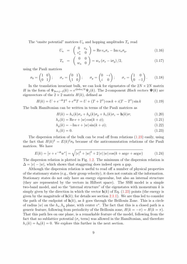
In the translation invariant bulk, we can look for eigenstates of the 2N × 2N matrixH in the form of Ψ2n+j−2(k) = ei2πkn/NΨj(k). The 2-component Bloch vectors Ψ(k) areeigenvectors of the 2× 2 matrix H(k), defined as
H(k) = U + e−ikT † + eikT = U + (T + T †) cos k + i(T − T †) sin k (1.19)
The bulk Hamiltonian can be written in terms of the Pauli matrices as
H(k) = hx(k)σx + hy(k)σy + hz(k)σz = h(k)σ; (1.20)
hx(k) = Re v + |w| cos(k + φ); (1.21)
hy(k) = −Im v + |w| sin(k + φ); (1.22)
hz(k) = 0. (1.23)
The dispersion relation of the bulk can be read off from relations (1.23) easily, usingthe fact that H(k)2 = E(k)2σ0 because of the anticommutation relations of the Paulimatrices. We have
E(k) =∣∣v + e−ikw∗
∣∣ =
√|v|2 + |w|2 + 2 |v| |w| cos(k + argv + argw) (1.24)
The dispersion relation is plotted in Fig. 1.2. The minimum of the dispersion relation is∆ = |v| − |w|, which shows that staggering does indeed open a gap.
Although the dispersion relation is useful to read off a number of physical propertiesof the stationary states (e.g., their group velocity), it does not contain all the information.Stationary states do not only have an energy eigenvalue, but also an internal structure(they are represented by the vectors in Hilbert space). The SSH model is a simpletwo-band model, and so the “internal structure” of the eigenstates with momentum k issimply given by the direction in which the vector h(k) of Eq. (1.23) points (the energy isgiven by the magnitude of h(k); for details see section 2.1.1). We are thus led to considerthe path of the endpoint of h(k), as k goes through the Brillouin Zone. This is a circleof radius |w| on the hx, hy plane, with center v∗. The fact that this is a closed path is ageneric feature, following from periodicity of the Brillouin zone, H(k = −π) = H(k = π).That this path lies on one plane, is a remarkable feature of the model, following from thefact that no sublattice potential (σz term) was allowed in the Hamiltonian, and thereforehz(k) = h0(k) = 0. We explore this further in the next section.
9

1.2.2 Chiral symmetry
The Hamiltonian of the SSH model, including bulk and boundary, Eq. (1.3) is bipartite.By this we mean that we can assign each site one of the sublattice indices A or B, suchthat the Hamiltonian includes no transitions between sites with the same index. In thiscase, this sublattice index is the same as the index denoted by j in the previous section.Formally, we can define the projectors on the sublattices using the notation of Eq. (1.10)as
PA =∑r=2n
|r〉 〈r| ; (1.25)
PB =∑
r=2n+1
|r〉 〈r| . (1.26)
We define the “coloring” operator
Σz = PA − PB. (1.27)
The matrix elements of Σz vanish, 〈r|Σz |s〉 = 0, if sites r and s are in different unitcells (even within a unit cell if r 6= s, but this is not important here). In that sense theoperator Σz is local, i.e., it does not mix sites between unit cells. Therefore it can berepresented in terms of a matrix acting within each unit cell:
Σz = σz ⊕ σz ⊕ . . .⊕ σz =N⊕n=1
σz. (1.28)
Thus Σz inherits its algebra from σz,
Σ†zΣz = 1; (1.29)
Σ2z = 1; (1.30)
There are no onsite terms in the Hamiltonian, and therefore, independent of the valuesof the hopping amplitudes tj, the operator Σz anticommutes with the Hamiltonian:
ΣzHΣz = −H. (1.31)
This anticommutation relation holds for the same chiral symmetry operator if the hop-ping amplitudes depend on the position. The properties of locality, unitarity, hermiticity,and the anticommutation relation (1.31) together ensure that Σz is a unitary represen-tation of chiral symmetry.
If chiral symmetry is to be useful for topological protection, as we are going to useit later on, it has to be robust. Many of the parameters of a Hamiltonian are subject to(local) disorder. In the SSH model, this is the case with the hopping amplitudes. We can
10

formally gather all parameters subject to disorder in a vector ξ. Instead of talking aboutthe symmetries of a Hamiltonian H, we should rather refer to symmetries of a set ofHamiltonians H(ξ), for all ξ from some ensemble. We can then claim that this set haschiral symmetry represented by Σz if all Hamiltonians in the set have chiral symmetry.
It can happen that a Hamiltonian is not bipartite, but only because of an unluckychoice of coordinates. Therefore, in the definition of chiral symmetry, before applyingthe “coloring operator” Σz, we can allow for a basis transformation via a unitary matrixU , independent of ξ, and local (not exchanging sites between unit cells). We then define
Γ = U †ΣzU. (1.32)
The relations of locality, unitarity, hermiticity, and the anticommutation relation can betranscribed from (1.31):
Γ =N∑n=1
Γ1; (1.33)
Γ† = Γ = Γ−1; (1.34)
ΓHΓ = −H. (1.35)
We included the requirement that Γ should take a direct sum form in the sense ofEq. (1.28). It can be shown that if there is a local, ξ-independent operator Γ such thatEqs. (1.33), (1.34), (1.35) hold, one can always construct a basis transformation unitaryoperator U to have chiral symmetry represented by Σz.
A straightforward consequence of chiral symmetry is that the spectrum of H is sym-metric. For eigenstates |ψn〉 of H, we have
H |ψn〉 = En |ψn〉 ; (1.36)
HΓ |ψn〉 = −ΓH |ψn〉 = −ΓEn |ψn〉 = −EnΓ |ψn〉 . (1.37)
For any eigenstate of the SSH model with nonzero energy, flipping the sign of thewavefunction on the odd sites gives another eigenstate with opposite energy. Since theseeigenstates have different energy, their wavefunctions have to be orthogonal. This impliesthat every nonzero energy eigenstate of H has equal support on both sublattices. Incontrast, 0 energy eigenstates can be their own chiral symmetric partners: these areeigenstates of Σz, and therefore have support on only one sublattice.
1.2.3 Bulk winding number
The path of the endpoint of h(k), as k goes through the Brillouin Zone, is a closed pathon the hx, hy plane, and the origin, h = 0, cannot be on the path (there is no gap ifh = 0). To a closed path on the plane that does not contain the origin, we can associate a
11
winding number ν. This is the number of times the path encircles the origin, the windingof the complex number hx(k) + ihy(k) as the wavenumber k is swept across the BrillouinZone, k = −π → π. To write this in a compact formula, note that H(k) is off-diagonalfor any k:
H(k) =
(0 h(k)
h∗(k) 0
); h(k) = hx(k)− ihy(k). (1.38)
The winding of h(k) is the same as the winding number of the complex number h(k).This can be written as an integral, using the complex logarithm function, log(|h| eiargh) =log |h|+ iargh. It is easy to check that
ν =1
2πi
∫ π
−πdk
d
dklog h(k). (1.39)
The above integral is always real, since |h(k = −π)| = |h(k = π)|.In general, for 1D chains with more complex unit cells, and a higher number of bands,
say, 2n, the above formula generalizes in the following way. We fix a basis where chiralsymmetry is represented by Σz = diag (1, . . . , 1︸ ︷︷ ︸
n
,−1, . . . ,−1︸ ︷︷ ︸n
). In this basis H(k) has the
block off-diagonal form above, with h(k) a n×n matrix. Without proof, we remark thatreplacing log h(k) with log deth(k) in the formula above gives a topological invariant,the winding number ν.
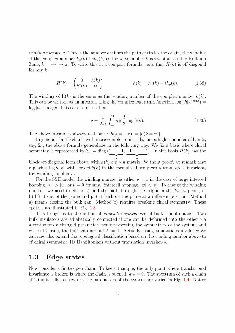
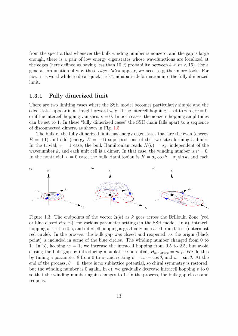
For the SSH model the winding number is either ν = 1 in the case of large intercellhopping, |w| > |v|, or ν = 0 for small intercell hopping, |w| < |v|. To change the windingnumber, we need to either a) pull the path through the origin in the hx, hy plane, orb) lift it out of the plane and put it back on the plane at a different position. Methoda) means closing the bulk gap. Method b) requires breaking chiral symmetry. Theseoptions are illustrated in Fig. 1.3
This brings us to the notion of adiabatic equivalence of bulk Hamiltonians. Twobulk insulators are adiabatically connected if one can be deformed into the other viaa continuously changed parameter, while respecting the symmetries of the system, andwithout closing the bulk gap around E = 0. Actually, using adiabatic equivalence wecan now also extend the topological classification based on the winding number above toof chiral symmetric 1D Hamiltonians without translation invariance.
1.3 Edge states
Now consider a finite open chain. To keep it simple, the only point where translationalinvariance is broken is where the chain is opened, wN = 0. The spectrum of such a chainof 20 unit cells is shown as the parameters of the system are varied in Fig. 1.4. Notice
12
from the spectra that whenever the bulk winding number is nonzero, and the gap is largeenough, there is a pair of low energy eigenstates whose wavefunctions are localized atthe edges (here defined as having less than 10 % probability between 4 < m < 16). For ageneral formulation of why these edge states appear, we need to gather more tools. Fornow, it is worthwhile to do a “quick trick”: adiabatic deformation into the fully dimerizedlimit.
1.3.1 Fully dimerized limit
There are two limiting cases where the SSH model becomes particularly simple and theedge states appear in a straightforward way: if the intercell hopping is set to zero, w = 0,or if the intercell hopping vanishes, v = 0. In both cases, the nonzero hopping amplitudescan be set to 1. In these “fully dimerized cases” the SSH chain falls apart to a sequenceof disconnected dimers, as shown in Fig. 1.5.
The bulk of the fully dimerized limit has energy eigenstates that are the even (energyE = +1) and odd (energy E = −1) superpositions of the two sites forming a dimer.In the trivial, v = 1 case, the bulk Hamiltonian reads H(k) = σx, independent of thewavenumber k, and each unit cell is a dimer. In that case, the winding number is ν = 0.In the nontrivial, v = 0 case, the bulk Hamiltonian is H = σx cos k + σy sin k, and each
Figure 1.3: The endpoints of the vector h(k) as k goes across the Brillouin Zone (redor blue closed circles), for various parameter settings in the SSH model. In a), intracellhopping v is set to 0.5, and intercell hopping is gradually increased from 0 to 1 (outermostred circle). In the process, the bulk gap was closed and reopened, as the origin (blackpoint) is included in some of the blue circles. The winding number changed from 0 to1. In b), keeping w = 1, we increase the intracell hopping from 0.5 to 2.5, but avoidclosing the bulk gap by introducing a sublattice potential, Hsublattice = uσz. We do thisby tuning a parameter θ from 0 to π, and setting v = 1.5− cos θ, and u = sin θ. At theend of the process, θ = 0, there is no sublattice potential, so chiral symmetry is restored,but the winding number is 0 again, In c), we gradually decrease intracell hopping v to 0so that the winding number again changes to 1. In the process, the bulk gap closes andreopens.
13
dimer is shared between two neighboring unit cells. In this nontrivial case, the windingnumber is ν = 1. In both cases, H(k)2 = 1, showing that the bulk has flat bands, withzero group velocity. This indicates that the energy eigenstates are localized, which isclearly the case: each eigenstate resides on its own dimer.
At the ends of an open, nontrivial fully dimerized chain, there is one 0 energy edgestate (one on each end of the chain, two in total). When the edge is created by setting anintercell hopping amplitude to 0, in the nontrivial case, at each edge, a dimer is cut intotwo monomers, one half of which is left “inside” the chain. Since no onsite potentials areallowed (these would break chiral symmetry), the energy eigenstates on these monomershave 0 energy. In contrast, a trivial fully dimerized chain already has edges built intothe Hamiltonian, and therefore has no 0 energy edge states.
1.3.2 Adiabatic deformation
Although the fully dimerized limits represent two very special cases of the SSH model,they are exhaustive in the sense that any generic SSH Hamiltonian is adiabatically con-nected to either the one or the other. To see what we mean by “adiabatically connected”,consider a generic insulating SSH Hamiltonian, with a translationally invariant bulk(with staggered hopping amplitudes) and two open ends, with arbitrary end regions.Now consider continuously decreasing the weaker hopping amplitude to 0, then changingthe phase of the stronger hopping amplitude to 0, then changing the magnitude of the
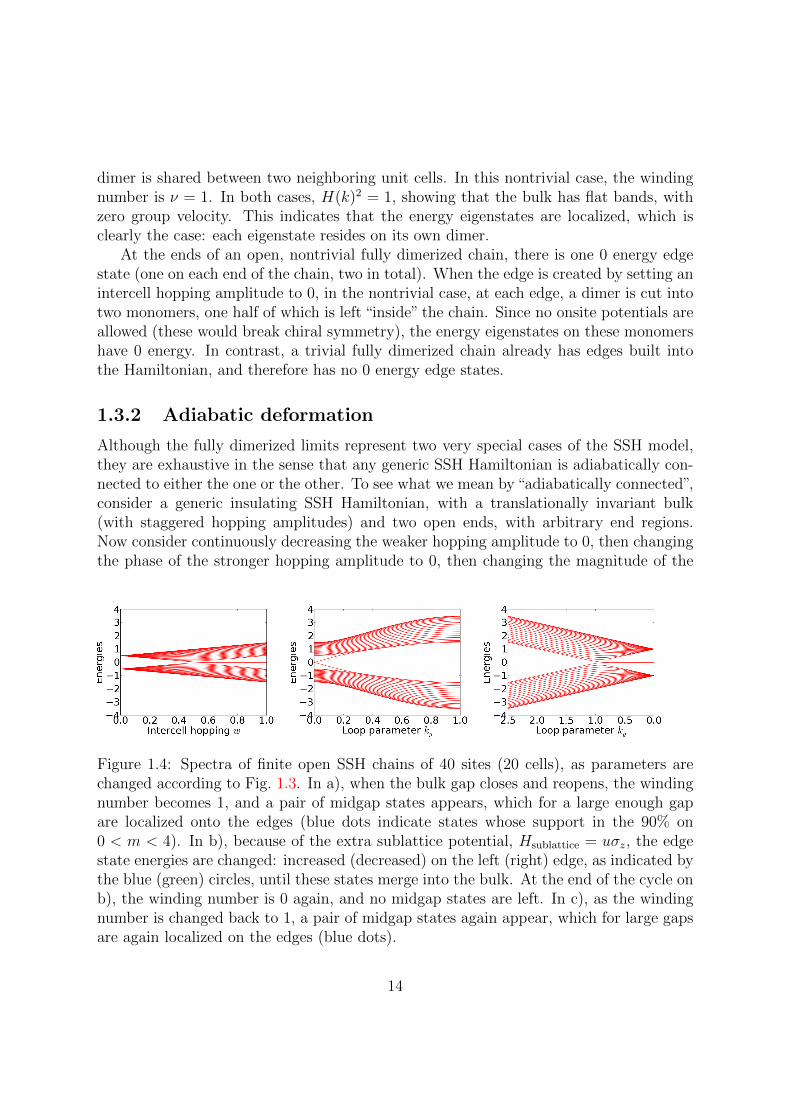
Figure 1.4: Spectra of finite open SSH chains of 40 sites (20 cells), as parameters arechanged according to Fig. 1.3. In a), when the bulk gap closes and reopens, the windingnumber becomes 1, and a pair of midgap states appears, which for a large enough gapare localized onto the edges (blue dots indicate states whose support in the 90% on0 < m < 4). In b), because of the extra sublattice potential, Hsublattice = uσz, the edgestate energies are changed: increased (decreased) on the left (right) edge, as indicated bythe blue (green) circles, until these states merge into the bulk. At the end of the cycle onb), the winding number is 0 again, and no midgap states are left. In c), as the windingnumber is changed back to 1, a pair of midgap states again appear, which for large gapsare again localized on the edges (blue dots).
14
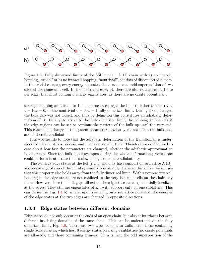
Figure 1.5: Fully dimerized limits of the SSH model. A 1D chain with a) no intercellhopping, “trivial”or b) no intracell hopping, “nontrivial”, consists of disconnected dimers.In the trivial case, a), every energy eigenstate is an even or an odd superposition of twosites at the same unit cell. In the nontrivial case, b), there are also isolated cells, 1 siteper edge, that must contain 0 energy eigenstates, as there are no onsite potentials. .
stronger hopping amplitude to 1. This process changes the bulk to either to the trivialv = 1, w = 0, or the nontrivial v = 0, w = 1 fully dimerized limit. During these changes,the bulk gap was not closed, and thus by definition this constitutes an adiabatic defor-mation of H. Finally, to arrive to the fully dimerized limit, the hopping amplitudes atthe edge regions can be set to continue the pattern of the bulk up until the very end.This continuous change in the system parameters obviously cannot affect the bulk gap,and is therefore adiabatic.
It is worthwhile to note that the adiabatic deformation of the Hamiltonian is under-stood to be a fictitious process, and not take place in time. Therefore we do not need tocare about how fast the parameters are changed, whether the adiabatic approximationholds or not. Since the bulk gap stays open during the whole deformation process, onecould perform it at a rate that is slow enough to ensure adiabaticity.
The 0 energy edge states at the left (right) end only have support on sublattice A (B),and so are eigenstates of the chiral symmetry operator Σz. Later in the course, we will seethat this property also holds away from the fully dimerized limit. With a nonzero intercellhopping v, the edge states are not confined to the very last unit cells on the chain anymore. However, since the bulk gap still exists, the edge states, are exponentially localizedat the edges. They still are eigenstates of Σz, with support only on one sublattice. Thiscan be seen in Fig. 1.4 b), where, upon switching on a sublattice potential, the energiesof the edge states at the two edges are changed in opposite directions.
1.3.3 Edge states between different domains
Edge states do not only occur at the ends of an open chain, but also at interfaces betweendifferent insulating domains of the same chain. This can be understood via the fullydimerized limit, Fig. 1.6. There are two types of domain walls here: those containingsingle isolated sites, which host 0 energy states on a single sublattice (no onsite potentialsare allowed), and those containing trimers. On a trimer, the odd superposition of the
15
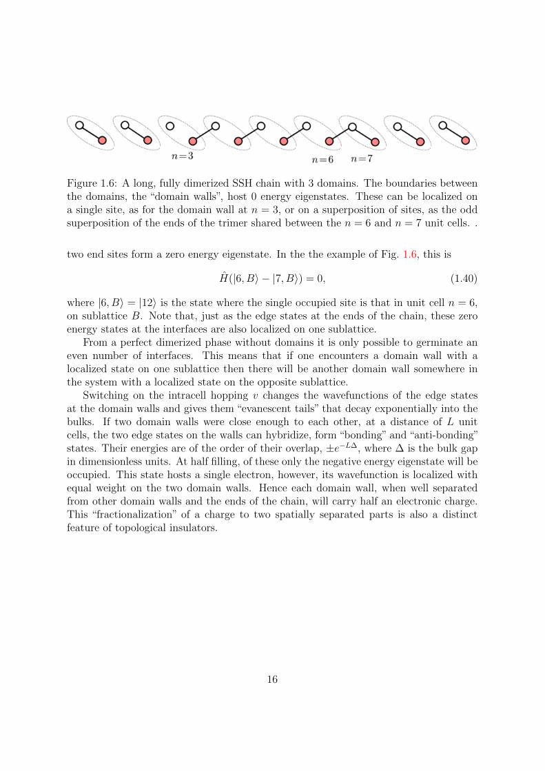
Figure 1.6: A long, fully dimerized SSH chain with 3 domains. The boundaries betweenthe domains, the “domain walls”, host 0 energy eigenstates. These can be localized ona single site, as for the domain wall at n = 3, or on a superposition of sites, as the oddsuperposition of the ends of the trimer shared between the n = 6 and n = 7 unit cells. .
two end sites form a zero energy eigenstate. In the the example of Fig. 1.6, this is
H(|6, B〉 − |7, B〉) = 0, (1.40)
where |6, B〉 = |12〉 is the state where the single occupied site is that in unit cell n = 6,on sublattice B. Note that, just as the edge states at the ends of the chain, these zeroenergy states at the interfaces are also localized on one sublattice.
From a perfect dimerized phase without domains it is only possible to germinate aneven number of interfaces. This means that if one encounters a domain wall with alocalized state on one sublattice then there will be another domain wall somewhere inthe system with a localized state on the opposite sublattice.
Switching on the intracell hopping v changes the wavefunctions of the edge statesat the domain walls and gives them “evanescent tails” that decay exponentially into thebulks. If two domain walls were close enough to each other, at a distance of L unitcells, the two edge states on the walls can hybridize, form “bonding” and “anti-bonding”states. Their energies are of the order of their overlap, ±e−L∆, where ∆ is the bulk gapin dimensionless units. At half filling, of these only the negative energy eigenstate will beoccupied. This state hosts a single electron, however, its wavefunction is localized withequal weight on the two domain walls. Hence each domain wall, when well separatedfrom other domain walls and the ends of the chain, will carry half an electronic charge.This “fractionalization” of a charge to two spatially separated parts is also a distinctfeature of topological insulators.
16

Chapter 2
Berry phase and polarization
The SSH model was a concrete example for a 1D topological insulator. We have seenhow the bulk–boundary correspondance works: At the interfaces between two bulks withdifferent topological invariants, there were low energy states protected by the global chiralsymmetry. These low energy midgap states are 0 dimensional: they extend slightly intothe bulks, with exponentially decaying tails, but other than that, they just are there,and do nothing spectacular. (Although closely related edge states in a a topologicalsuperconductor wire can be used for quantum information processing).
In higher dimensional topological insulators, edge states can have a wider range ofproperties. In two dimensions, they can propagate along the 1D edge, and their propa-gation is reflectionless. Higher dimensional lattice systems have more complicated topo-logical invariants than the winding number in the SSH model. The first step towardsunderstanding these invariants is the adiabatic Berry phase.
2.1 Berry phase, Berry connection, Berry curvature
We introduce the Berry phase in the most general setting, and use examples to illustrateits properties.
2.1.1 Fixing the gauge
Take a physical system with parameters R = (R1, R2, . . . , RN), that are real numbers.We denote the Hamiltonian by H(R), and its eigenstates, ordered according to theenergies En(R), by |n(R)〉:
H(R) |n(R)〉 = En(R) |n(R)〉 . (2.1)
We call |n(R)〉 the snapshot basis. The above definition requires fixing the arbitraryphase prefactor for every |n(R)〉. This is gauge fixing, and since this is very importantfor what follows, let’s see how it works for a specific example.
17

Spin-1/2: No “nice” global gauge
A simple but important example is the most general 2-level Hamiltonian,
H(R) = h0(R)σ0 + h1(R)σx + h2(R)σy + h3(R)σz = h0(R)σ0 + h(R)σ, (2.2)
with real functions hj(R). The value of h0 does not affect the eigenstate |n(R)〉, andtherefore we set it to 0 for simplicity. Because of the anticommutation relations of thePauli matrices, the Hamiltonian squares to a multiple of the identity operator, H(R)2 =h2 ∈ R, and so the spectrum of H(R) is symmetric: For any choice of R it is ±
√h2.
We want to characterize the eigenstates, and so the value of the energy is irrelevant: weintroduce the unit vector
h = h/√
h2. (2.3)
The endpoints of h map out the surface of a unit sphere, called the Bloch sphere,shown in Fig. 2.1. One point on the sphere can be parametrized by the usual sphericalangles θ ∈ [0, π) and ϕ ∈ [0, 2π), as
cos θ = h3; (2.4)
eiϕ =h1 + ih2√h2
1 + h22
. (2.5)
The eigenstate with E = + |h| of the corresponding Hamiltonian is:∣∣∣n(h)⟩
=∣∣∣h⟩ = eiα(θ,ϕ)
(e−iϕ/2 cos θ/2eiϕ/2 sin θ/2
). (2.6)
We explicitly pulled out the free phase factor in front of the vector. Fixing this phase
factor corresponds to fixing a gauge. The eigenstate with E = − |h| is∣∣∣n(−h)
⟩.
Consider fixing α = 0. This is appealing because both θ and ϕ carry factors of 1/2.However, fixing θ, let us make a full circle in parameter space: ϕ = 0→ 2π. We shouldcome back to the same Hilbert space vector, and we do, but we also pick up a phase of−1. We can either say that this choice of gauge led to a discontinuity at ϕ = 0, or thatour representation is not single-valued. One might think that there are ways to fix this,however.
Let us fix α = ϕ/2. This gives an additional factor of −1 as we make the circle in ϕ,and so it seems we have a continuous, single valued representation:∣∣∣h⟩
S=
(cos θ/2eiϕ sin θ/2
). (2.7)
18
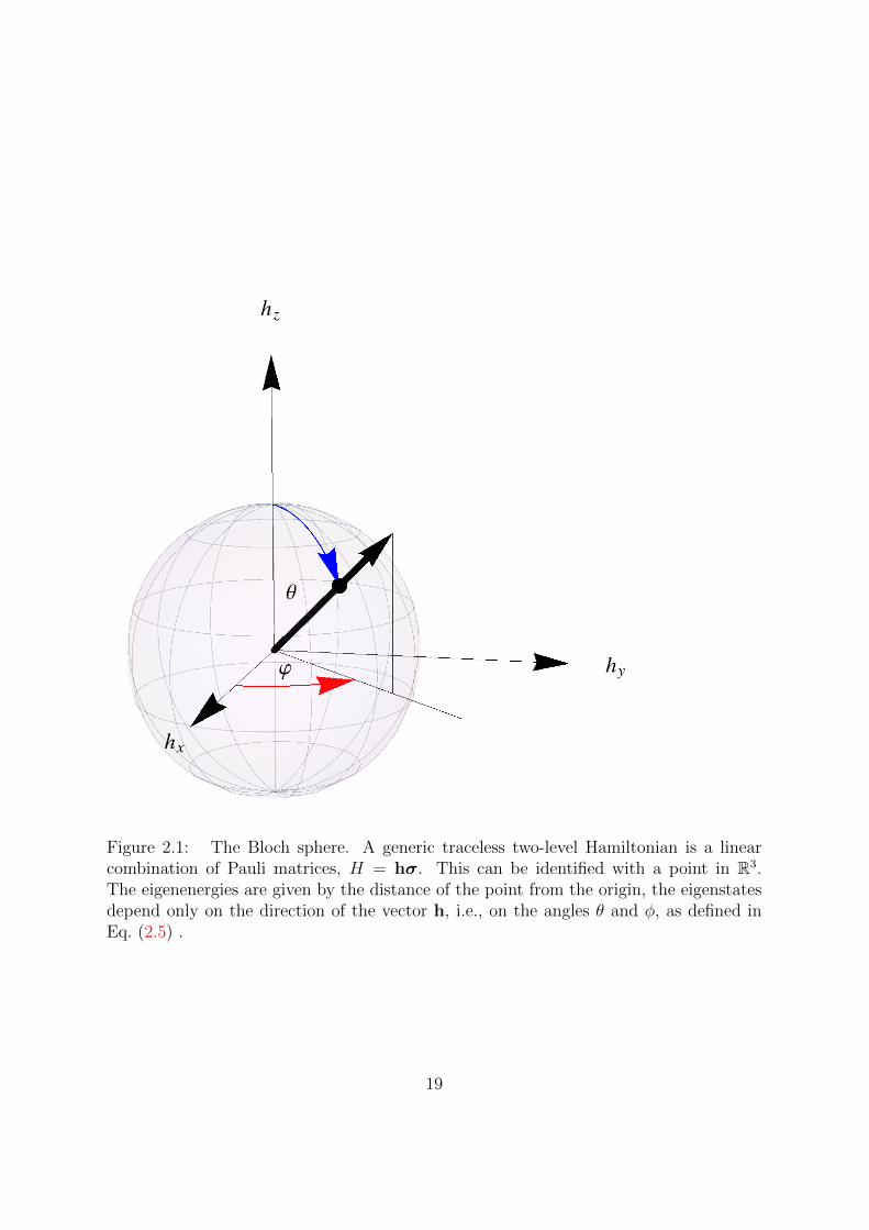
Figure 2.1: The Bloch sphere. A generic traceless two-level Hamiltonian is a linearcombination of Pauli matrices, H = hσ. This can be identified with a point in R3.The eigenenergies are given by the distance of the point from the origin, the eigenstatesdepend only on the direction of the vector h, i.e., on the angles θ and φ, as defined inEq. (2.5) .
19
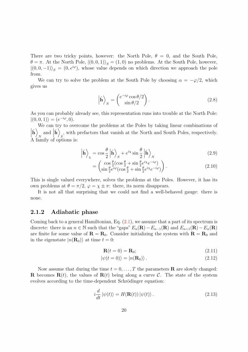
There are two tricky points, however: the North Pole, θ = 0, and the South Pole,θ = π. At the North Pole, |(0, 0, 1)〉S = (1, 0) no problems. At the South Pole, however,|(0, 0,−1)〉S = (0, eiϕ), whose value depends on which direction we approach the polefrom.
We can try to solve the problem at the South Pole by choosing α = −ϕ/2, whichgives us ∣∣∣h⟩
N=
(e−iϕ cos θ/2
sin θ/2
). (2.8)
As you can probably already see, this representation runs into trouble at the North Pole:|(0, 0, 1)〉 = (e−iϕ, 0).
We can try to overcome the problems at the Poles by taking linear combinations of∣∣∣h⟩N
and∣∣∣h⟩
S, with prefactors that vanish at the North and South Poles, respectively.
A family of options is: ∣∣∣h⟩χ
= cosθ
2
∣∣∣h⟩S
+ eiχ sinθ
2
∣∣∣h⟩N
(2.9)
=
(cos θ
2(cos θ
2+ sin θ
2eiχe−iϕ)
sin θ2eiϕ(cos θ
2+ sin θ
2eiχe−iϕ)
). (2.10)
This is single valued everywhere, solves the problems at the Poles. However, it has itsown problems at θ = π/2, ϕ = χ± π: there, its norm disappears.
It is not all that surprising that we could not find a well-behaved gauge: there isnone.
2.1.2 Adiabatic phase
Coming back to a general Hamiltonian, Eq. (2.1), we assume that a part of its spectrum isdiscrete: there is an n ∈ N such that the “gaps”En(R)−En−1(R) and En+1(R)−En(R)are finite for some value of R = R0. Consider initializing the system with R = R0 andin the eigenstate |n(R0)〉 at time t = 0:
R(t = 0) = R0; (2.11)
|ψ(t = 0)〉 = |n(R0)〉 . (2.12)
Now assume that during the time t = 0, . . . , T the parameters R are slowly changed:R becomes R(t), the values of R(t) being along a curve C. The state of the systemevolves according to the time-dependent Schrodinger equation:
id
dt|ψ(t)〉 = H(R(t)) |ψ(t)〉 . (2.13)
20

Further, assume that R is varied in such a way that at all times the energy gapsaround the state |n(R(t))〉 remain finite. On the other hand, the rate of variation ofR(t) along path C has to be slow enough compared to the frequencies corresponding tothe energy gap, and then the adiabatic approximation holds (for the precise conditions,see [6]). In that case, the system remains in the energy eigenstate |n(R(t))〉, only pickingup a phase. Using this adiabatic approximation, take as Ansatz
|ψ(t)〉 = eiγn(t)e−i∫ t0 En(R(t′))dt′ |n(R(t))〉 . (2.14)
Insert this Ansatz into the Schrodinger equation (2.13), we have for the left hand side
id
dt|ψ(t)〉 = eiγn(t)e−i
∫ t0 En(R(t′))dt′(−dγndt|n(R(t))〉+ En(R(t)) |nR(t)〉+ i
∣∣∣∣ ddtn(R(t))
⟩). (2.15)
To see what we mean by∣∣ ddtn(R(t))
⟩, we write it out explicitly in terms of a fixed basis.
For better readability, in the following we often drop the t argument of R(t).
|m〉0 ≡ |m(R0)〉 ; (2.16)
|n(R)〉 =∑m
cm(R) |m〉0 ; (2.17)∣∣∣∣ ddtn(R(t))
⟩=dR
dt· |∇Rn(R)〉 =
dR
dt
∑m
∇Rcm(R) |m〉0 . (2.18)
We insert the Ansatz (2.14) into the rhs of the Schrodinger equation (2.13), use
H(R) |n(R)〉 = En(R) |n(R)〉 , (2.19)
simplify and reorder the Schrodinger equation, we obtain
−(d
dtγn
)|n〉+ i
∣∣∣∣ ddtn⟩
= 0. (2.20)
Multiply from the left by 〈n(R(t))|, and obtain
d
dtγn(t) = i
⟨n(R(t))
∣∣∣∣ ddtn(R(t))
⟩=dR
dti 〈n(R) | ∇Rn(R)〉 . (2.21)
For the last equality we used that the only dependence on time is via the parameters R.We have found that for a path in parameter space C, traced out by R(t), there is an
adiabatic phase γn(C) associated with it,
γn(C) =
∫C
i 〈n(R) | ∇Rn(R)〉 dR. (2.22)
21
Where did we use the adiabatic approximation?
On the face of it, our derivation seems to do too much. We have produced an exactsolution of the Schrodinger equation. Where did we use the adiabatic approximation?
In fact, Eq. (2.21) does not imply Eq. (2.20). For the more complete derivation,showing how the nonadiabatic terms appear, see [6].
2.1.3 Berry phase
Berry connection
We define the integrand of Eq. (2.22) as the Berry connection or Berry vector potential :
A(n)(R) = i 〈n(R) | ∇Rn(R)〉 = −Im 〈n(R) | ∇Rn(R)〉 , (2.23)
where the second equality follows from the conservation of the norm, ∇R 〈n(R) | n(R)〉 =0.
Gauge dependence
As the name “vector potential” suggests, the Berry connection is not gauge invariant.Consider a gauge transformation:
|n(R)〉 → eiα(R) |n(R)〉 : (2.24)
A(n)(R)→ A(n)(R)−∇Rα(R). (2.25)
Therefore, in the generic case, the adiabatic phase cannot be observed.
Adiabatic phase of a closed loop is observable: the Berry phase
To get the adiabatic phase to have physical consequences, we need to have an in-terferometric setup. This means coherently splitting the wavefunction of the systeminto two parts, taking them through two adiabatic trips in parameter space, via R(t)and R′(t), and bringing the parts back together. The two parts can interfere only if|n(R(T ))〉 = |n(R′(T ))〉, which is typically ensured if R(T ) = R′(T ). The difference inthe adiabatic phases γn and γ′n is the adiabatic phase associated with the closed loop C,which is the path of t→ R(t)Θ(T − t) + R(2T − t)Θ(t− T ).
Although the adiabatic phase of a general path in parameter space is gauge dependent,for a closed loop C, it is gauge invariant. This is obvious, since a gauge transformationis single valued, but can also be proven via the Stokes theorem. The adiabatic phase ofthe loop, the integral of A around the closed loop, is the Berry phase.
22

2.1.4 Berry curvature
We calculated the Berry phase using the gauge dependent Berry connection. However,since the final result was gauge independent, there should be a gauge independent wayto calculate it. This is provided by the Berry curvature.
We define the Berry curvature
B(n)(R) = ∇R ×A(n)(R). (2.26)
In the following, we drop the index (n), and the argument R for better readability,wherever this leads to no confusion. We also use ∇ for ∇R.
Then, by virtue of the Stokes theorem, we have for the Berry phase,
γn(C) =
∫S
B(n)(R)dS, (2.27)
where S is any surface whose boundary is the loop C.We use 3D notation here, but the above equations can be generalized for any dimen-
sionality of R.The Berry curvature B is very much like a magnetic field. For instance, ∇B = 0,
from definition (2.26).Berry provided [4] two practical formulas for the Berry curvature. First,
Bj = −Im εjkl ∂k 〈n | ∂ln〉 = −Im εjkl 〈∂kn | ∂ln〉+ 0, (2.28)
where the second term is 0 because ∂k∂l = ∂l∂k but εjkl = −εjlk.To obtain Berry’s second formula, inserting a resolution of identity in the snapshot
basis in the above equation, we obtain
B(n) = −Im∑n′ 6=n
〈∇n | n′〉 × 〈n′ | ∇n〉 . (2.29)
The term with n′ = n is omitted from the sum, as it is zero, since because of theconservation of the norm of |n〉, 〈∇n | n〉 = −〈n | ∇n〉. To calculate 〈n′ | ∇n〉, startfrom the definition of the eigenstate |n〉, act on both sides with ∇R, and then projectunto |n′〉:
H(R) |n〉 = En |n〉 ; (2.30)
(∇H(R)) |n〉+H(R) |∇n〉 = (∇En) |n〉+ En |∇n〉 ; (2.31)
〈n′| ∇H |n〉+ 〈n′|H |∇n〉 = 0 + En 〈n′ | ∇n〉 . (2.32)
Act with H towards the left in Eq. (2.32), rearrange, substitute into (2.29), and youshould obtain the second form of the Berry curvature:
B(n) = −Im∑n′ 6=n
〈n| ∇H |n′〉 × 〈n′| ∇H |n〉(En − En′)2
. (2.33)
This shows that the monopole sources of the Berry curvature, if they exist, are thepoints of degeneracy.
23
2.2 Electronic polarization and Berry phase in a 1D
crystal
We now apply the concept of Berry phase on an insulator by formally treating thewavenumber k as an externally controlled parameter. A lattice model in 1D is specifiedby giving the bulk Hamiltonian as a function of the wavenumber H(k), with the energybands |n(k)〉,
H(k) |n(k)〉 = En(k) |n(k)〉 . (2.34)
Formally, we can treat k as a parameter and tune it across the Brillouin Zone: k =−π, . . . , π. Since H(−π) = H(π), to each nondegenerate band n we can associate aBerry phase:
γn = i
∫BZ
dk 〈n(k)| ddk|n(k)〉 . (2.35)
This generalization of the Berry phase is known as Zak phase.Although the Zak phase is defined above by a completely formal procedure, which
does not correspond to an experimental situation, it does have physical significance: itgives the contribution of the band n to the electric polarization. In suitable units, thebulk electric polarization can be defined as the sum of all the Zak phases of the occupiedbands,
P =∑n<0
γn. (2.36)
There are two simple ways to show this nontrivial statement [12]. One is to consider thechange in bulk polarization as some system parameter is tuned. The other way, whichwe briefly summarize below, shows that the Zak phase of band n gives the expectationvalue of the position of the electron in the Wannier state coming from band n centeredon an atom at the origin.
2.2.1 Bloch functions and Wannier states
To show the physical interpretation of the Zak phase, we need to go beyond the simplelattice model for a solid state. Instead, consider the full wavefunction of an electron ina periodic potential V (x), with x measured in units of the period, V (x+ 1) = V (x):[
1
2mp2 + V (x)
]Ψn(k, x) = En(k)Ψn(k, x). (2.37)
24
According to the Bloch theorem, this has the form
Ψn(k, x) = eikxun(k, x), (2.38)
where un is a cell periodic function:
un(k, x) = un(k, x+ 1). (2.39)
The Schrodinger equation rewritten for un reads
H(k, x)un(k, x) =
[1
2m(p+ k)2 + V (x)
]un(k, x) = En(k)un(k, x). (2.40)
We specify a periodic gauge, by requiring
Ψn(k +G, x) = Ψn(k, x) (2.41)
for any reciprocal lattice vector G = 2πl, with l integer. This entails
un(k +G, x) = e−iGxun(k, x). (2.42)
Thereby, even though un(k, x) and un(k +G, x) are eigenfunctions of different Hamilto-nians, they are related by a fixed unitary transformation, which allows us to relate theirphases to each other in a well defined way. Details of the definition of this “open-path”geometric phase can be found in Resta’s lecture notes, [12]. In the continuum limit, thephase reads
γn = i
∫ π
−πdk
∫ 1
0
dx un(k, x)∗∂kun(k, x). (2.43)
The energy eigenstates of electrons in a perfect lattice are given by the Bloch func-tions that are delocalized over the entire lattice. For energy eigenstates within a band,a unitary transformation can be defined that transforms to an orthonormal set of wave-functions Φ
(n)m (x), that are each localized around site m. Of course, these Wannier modes
are not energy eigenstates, but they are useful tools in solid state physics. The definitionof Wannier states is the following:
wn(x) =1
2π
∫ π
−πdkΨn(k, x) =
1
2π
∫ π
−πdkeikxun(k, x); (2.44)
Φ(n)m (x) = wn(x−m). (2.45)
The inverse of the above transformation expresses the Bloch function in terms of theWannier states:
un(k, x) =∑m
e−ik(x−m)wn(x−m). (2.46)
25
Substituting the above relation into the definition of the Zak phase above, Eq. (2.43),we find
γn =
∫ 1
0
dx∑m,m′
wn(x−m)∗ (x−m′)wn(x−m′)∫ π
−πdkeik(m′−m)
=∑m
|wn(x−m)|2 (x−m) =
∫ ∞−∞
dx |φn(x)|2 x. (2.47)
The final result is that the Zak phase of the nth band, is the first moment of the center ofthe charge in the Wannier state centered on the atom at x = 0. This is a quantity whichcan be identified with the contribution of the band to the bulk electric polarization.
26
Chapter 3
Chern number
3.1 Reminder – Berry phase in a Two-level system
The simplest application of the Berry phase is a single two-level system, e.g., a singleelectron at a fixed point whose only degree of freedom is its spin (we could call this a “0-dimensional”system). There are no“position”or“momentum”variables, the Hamiltoniansimply reads
H(h) = hσ, (3.1)
As long as h 6= 0, the two energy eigenstates have different energy. Its two eigenstatesare |±,h〉, defined by
hσ |+,h〉 =√
h2 |+,h〉 ; hσ |−,h〉 = −√
h2 |−,h〉 . (3.2)
Now take a closed curve C in the parameter space R3. We are going to calculate theBerry phase γ− of the |−,h〉 eigenstate on this curve:
γ−(C) =
∮C
A(h)dh, (3.3)
with the Berry vector potential defined as
A(h) = i 〈−,h| ∇h |−,h〉 . (3.4)
The calculation becomes straightforward if we use the Berry curvature,
B(h) = ∇h ×A(h); (3.5)
γ−(C) =
∫S
B(h)dS, (3.6)
27
where S is any surface whose boundary is the loop C. (Alternatively, it is a worthwhileexercise to calculate the Berry phase directly in a fixed gauge, e.g., one of the threegauges of the previous chapter.)
Specifically, we make use of Berry’s gauge invariant formulation of the Berry curva-ture, derived in the last chapter (2.33):
B(n) = −Im∑n′ 6=n
〈n| ∇hH |n′〉 × 〈n′| ∇hH |n〉(En − En′)2
. (3.7)
In the case of the generic 2× 2 Hamiltonian (3.1) the above definition gives
B±(h) = −Im〈±|∇hH |∓〉 × 〈∓|∇hH |±〉
4h2, (3.8)
with
∇hH = σ. (3.9)
To evaluate (3.8), we choose the quantization axis parallel to h, thus the eigenstatessimply read
|+,h〉 =
(10
); |−,h〉 =
(01
). (3.10)
The matrix elements can now be computed as
〈−|σx |+〉 =(0 1
)(0 11 0
)(10
)= 1, (3.11)
and similarly,
〈−|σy |+〉 = i; (3.12)
〈−|σz |+〉 = 0. (3.13)
So the cross product of the vectors reads
〈−|σ |+〉 × 〈+|σ |−〉 =
1i0
× 1−i0
=
002i
. (3.14)
This gives us for the Berry curvature,
B±(h) = ± h
|h|1
2h2. (3.15)
28
We can recognize in this the field of a pointlike monopole source in the origin. Alludingto the analog between the Berry curvature and the magnetic field of electrodynamics(both are derived from a “vector potential”) we can refer to this field, as a “magneticmonopole”. Note however that this monopole exists in the abstract space of the vectorsh and not in real space.
The Berry phase of the closed loop C in parameter space, according to Eq. (3.6), isthe flux of the monopole field through a surface S whose boundary is C. It is easy toconvince yourself that this is half of the solid angle subtended by the curve,
γ−(C) =1
2ΩC. (3.16)
In other words, since the Berry phase is independent of the energies, we can project h onthe surface of a unit sphere, i.e., assume h2 = 1. This is the Bloch sphere, representingthe Hamiltonian hσ as well as the eigenstate |+〉. The Berry phase is half of the areaenclosed by this projected image of C, as illustrated in Fig. 3.1.
What about the Berry phase of the other energy eigenstate? From Eq. (3.8), thecorresponding Berry curvature B+ is obtained by inverting the order of the factors inthe cross product: this flips the sign of the cross product. Therefore the Berry phase
γ+(C) = −γ−(C). (3.17)
One can see the same result on the Bloch sphere. Since 〈+ | −〉 = 0, the point corre-sponding to |−〉 is antipodal to the point corresponding to |+〉. Therefore, the curvetraced by the |−〉 on the Bloch sphere is the inverted image of the curve traced by |+〉.These two curves have the same orientation, therefore the same area, with opposite signs.
In fact, a more general statement follows directly from Eq. (3.7), for a HamiltonianH with an arbitrary number of levels. If all the spectrum of H(R) is discrete along aclosed curve C, then one can add up the Berry phases of all the energy eigenstates. Thissum has to be 0, because∑
n
γn(C) =∑n
1
2π
∫S
B(n)(R)dS =1
2π
∫S
∑n
B(n)(R)dS; (3.18)
∑n
B(n) = −Im∑n
∑n′ 6=n
〈n| ∇RH |n′〉 × 〈n′| ∇RH |n〉(En − En′)2
(3.19)
= −Im∑n
∑n′<n
1
(En − En′)2
(〈n| ∇RH |n′〉 × 〈n′| ∇RH |n〉 (3.20)
+ 〈n′| ∇RH |n〉 × 〈n| ∇RH |n′〉)
= 0. (3.21)
29
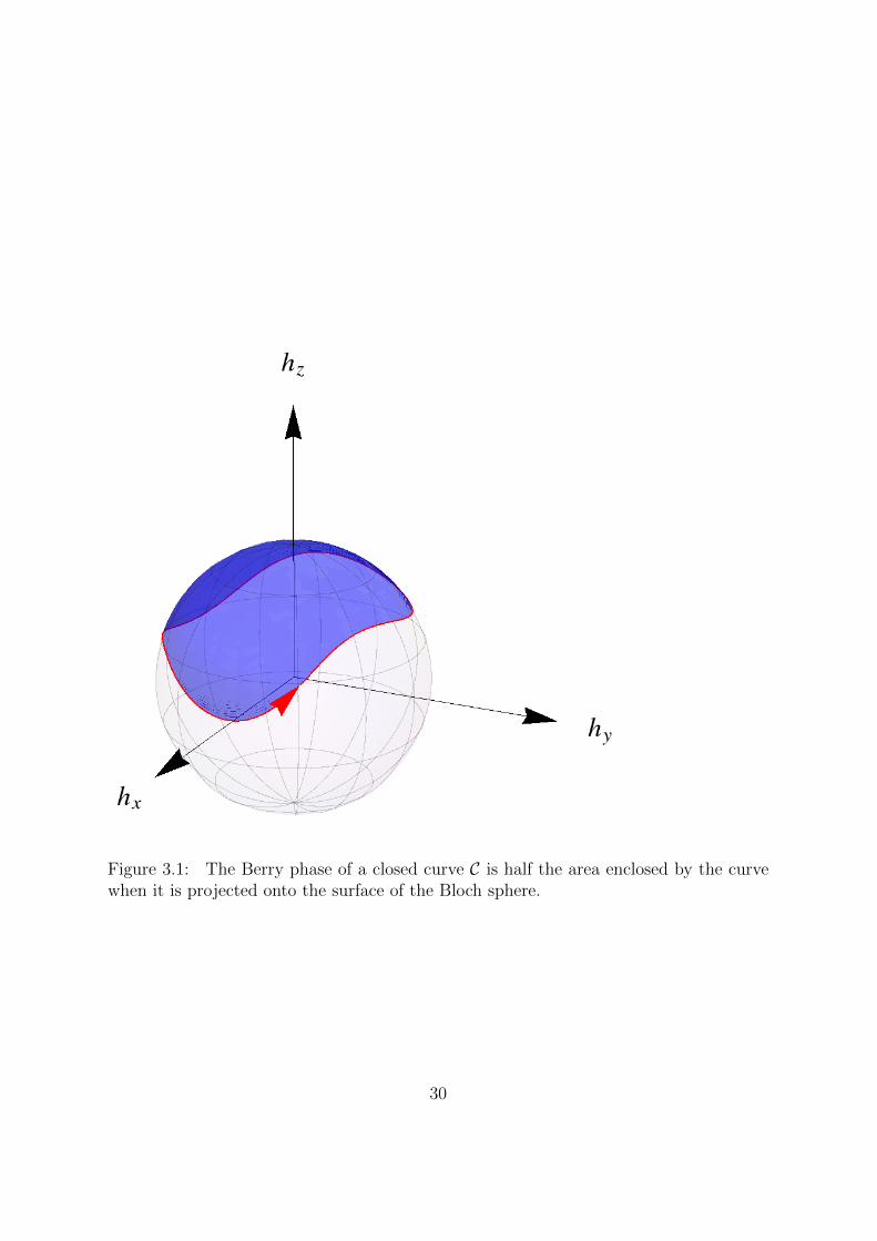
Figure 3.1: The Berry phase of a closed curve C is half the area enclosed by the curvewhen it is projected onto the surface of the Bloch sphere.
30
3.2 Chern number – General Definition
Take a Hamiltonian that depends continuously on some parameters R. Take a closedsurface S in the parameter space of R, such that the nth eigenstate of the Hamiltonianis nondegenerate on the surface. The integral of the Berry curvature of the energyeigenstate |n(k)〉 on that surface is the Chern number,
Q(n) = − 1
2π
∮S
B(n)dS. (3.22)
We are now going to prove that the Chern number is an integer. Take a simplyconnected closed loop C in the surface S. This cuts the surface into two parts: S1 andS2. The Berry phase associated to |n〉 on the loop can be calculated by integrating theBerry connection on the loop, or by integrating the Berry curvature on either of thesesurfaces. The resulting Berry phase, modulo 2π, is measurable, and therefore cannotdepend on which surface we integrated on,
γ(n) =
∮CA(n)dR =
∫S1
B(n)dS + 2πm1 =
∫S2
B(n)dS + 2πm2, (3.23)
where m1,m2 ∈ Z. The Chern number of the state |n〉 on the surface S is obtained byintegrating B(n) on the surfaces S1 and S2, but with opposite orientations of the surfaceelement,
Q(n) = − 1
2π
∮S
B(n)dS = − 1
2π
∮S1
B(n)dS +1
2π
∮S2
B(n)dS = m2 −m1. (3.24)
The Chern number is a topological invariant. Since the Chern number of a state |n〉on a closed surface S is an integer, it cannot change under smooth deformations of eitherthe Hamiltonian H or the surface S. The only way its value can change is if the gapcloses, i.e., the state |n〉 becomes degenerate with |n+ 1〉 or |n− 1〉 at some point on thesurface S.
3.2.1 Z-invariant: Chern number of a lattice Hamiltonian
As we did with the Berry phase, we are now going to apply the Chern number to a latticeHamiltonian, treating the wavenumbers (quasimomenta) k as tunable parameters. Takea lattice Hamiltonian on a 2-dimensional lattice,
H(kx, ky) |n(k)〉 = En |n(k)〉 (3.25)
Here the two wavenumbers are from the Brillouin Zone, k = (kx, ky) ∈ BZ, which is a2-dimensional torus, BZ = S1 × S1, since for any nx, ny ∈ Z,
|n(kx + 2nxπ, ky + 2nyπ)〉 = |n(kx, ky)〉 . (3.26)
31
As with the Berry phase, assume the nth energy eigenstate has an energy gap around itfor any (kx, ky). The Berry connection reads
A(n)j = −i 〈n(kx, ky)| ∂kj |n(kx, ky)〉 , for j = x, y. (3.27)
The Chern number of the n’th energy eigenstate is
Q(n) = − 1
2π
∫∫BZ
dkxdky
(∂A
(n)y
∂kx− ∂A
(n)x
∂ky
). (3.28)
The Chern number of a band of an insulator is a topological invariant. Its valuecannot change under smooth deformations of the parameters of the Hamiltonian, as longas at each k ∈ BZ, the energy of the band is distinct from the neighboring bands, i.e.,there are no direct band gap closings.
3.3 Two Level System
The simplest case where a Chern number can arise is a two-band system. Consider aparticle with two internal states, hopping on a 2D lattice. The two internal states canbe the spin of the conduction electron, but can also be some sublattice index of a spinpolarized electron. In the translation invariant bulk, the wavenumbers kx, ky are goodquantum numbers, and the Hamiltonian reads
H(kx, ky) = h(k)σ, (3.29)
with the function h(k) mapping a 2D vector from the Brillouin zone into a 3D vector.Since the Brillouin Zone is a torus, the endpoints of the vectors h(k) map out a deformedtorus in R3. This torus is a directed surface: its inside can be painted red, its outside,blue.
The Chern number of |−〉 is the flux of B−(h) through this torus. We have seenabove that B−(h) is the magnetic field of a monopole at the origin h = 0. If the origin ison the inside of the torus, this flux is +1. If it is outside of the torus, it is 0. If the torusis turned inside out, and contains the origin, the flux is -1. The torus can also intersectitself, and therefore contain the origin any number of times.
One way to count the number of times is to take any line from the origin to infinity,and count the number of times it intersects the torus, with a +1 for intersecting from theinside, and a -1 for intersecting from the outside. The sum is independent of the shapeof the line, as long as it goes all the way from the origin to infinity.
32

Figure 3.2: Sketch of the half BHZ model: a particle hopping on a square lattice.Each unit cell (circle) has two internal degrees of freedom. This can be rephrased as theparticle being a spinor, and the onsite potential U and the hopping amplitudes Tx andTy are 2× 2 matrices.
33

3.3.1 The “half BHZ” model
To illustrate the concepts of Chern number, we take a simple toy model introduced byBernevig, Hughes and Zhang, the “half BHZ” model. The attribute “half”, althoughsomewhat ambiguous at the moment, will attain clarity in a following chapter. Assketched in Fig. 3.2, the half BHZ model describes a spinor particle hopping on a lattice(equivalent to a structureless particle hopping on a bipartite lattice), with the followingHamiltonian:
H(k) = [∆ + cos kx + cos ky]σz + A(sin kxσx + sin kyσy). (3.30)
This Hamiltonian has a Zeeman splitting term, with energy ∆, a spin-z dependent hop-ping, with unit amplitude, and a spin-orbit coupling type term with amplitude A (whichwe set to 1 for most of the calculations). This last term corresponds to hopping with as-sociated spin flips: around the x axis for y direction hopping, and vice versa. Introducinga more general notation, we have
H(k) =1
2U + Txe
ikx + Tyeiky + h.c.; (3.31)
U = ∆σz; (3.32)
Tx =1
2σz −
iA
2σx; (3.33)
Ty =1
2σz −
iA
2σy. (3.34)
In real space generalization, with possibly site-dependent onsite and hopping terms,can be written using two-component cell indices n = (nx, ny), and unit vectors x = (1, 0)and y = (0, 1),
Hm,n = δm,nU(n) + δm−x,nTx(n) + δm,n−xTx(m)†
+ δm−y,nTy(n) + δm,n−yTy(m)†. (3.35)
On a lattice with Nx ×Ny unit cells, this includes periodic boundary conditions, e.g., ifTx and Ty are independent of n, and open boundary conditions, if Tx(Nx, ny) = 0 andTy(nx, Ny) = 0 for any nx, ny.
3.3.2 Dispersion relation
Making use of the algebraic properties of the Pauli matrices the bulk dispersion relationcan be easily calculated. The spectrum is simpliy given in terms of the magnitude of thevector
h(kx, ky) =
A sin kxA sin ky
∆ + cos kx + cos ky
. (3.36)
34

Thus
E±(kx, ky) = ±|h(kx, ky)| (3.37)
= ±√A2(sin2(kx) + sin2(ky)) + (∆ + cos(kx) + cos(ky))2. (3.38)
This spectrum is depicted for some special parameter values in Fig.3.3. As can beseen from the figure, by tuning of the parameters one can close and reopen gaps in thespectrum. If ∆ = −2, the energy gap closes at the center of the Brillouin Zone, i.e.,kx = ky = 0. In the vicinity of this so-called “Dirac point”, the dispersion relation hasthe shape of a “Dirac cone”. For ∆ = 2, we have a similar situation, with a Dirac coneat the corners of the Brillouin Zone, kx = ky = ±π. Since each corner is equally sharedbetween 4 Brillouin Zones, and we have 4 of them, this still leaves 1 Dirac point, 1 Diraccone per Brillouin Zone. For ∆ = 0, we find two Dirac cones: one at kx = 0, ky = ±πand a second one at kx = ±π, ky = 0. For all other values of ∆ the spectrum is gapped,and thus it makes sense to investigate the topological properties of the system.
3.3.3 Torus argument
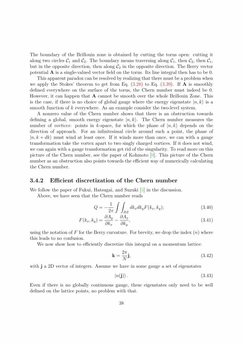
To calculate the Chern number for the valence band we shall employ the method discussedat the end of the last section. Namely we shall investigate how many times does the torusof the image of the Brillouin zone in the space of h contain the origin. To get some feelingabout the not so trivial geometry of the torus, it is instructive to follow a gradual sweepof the Brillouin zone in Fig. 3.4. The parameter ∆ shifts the whole torus along thez-direction, thus as we tune it we also control whether the origin is contained inside itor not. Generally three situations can occur as it is also depicted in Fig. 3.5. The toruseither does not contain the origin as in a) and d) and the Chern number is Q = 0 for|∆| > 2, or we can take a straight line to infinity from the origin that pierces the torusfirst from the blue side (outside) of the surface as in b) with Q = −1 for −2 < ∆ < 0,or piercing the torus from the red side (inside) as in c) with Q = 1 for 0 < ∆ < 2.
3.4 Chern number as an obstruction
3.4.1 An apparent paradox
One might think that the most straightforward way to calculate the Chern number byjust integrating the Berry vector potential around the Brillouin Zone. Applying Stokes’theorem to Eq. (3.28) we get
Q(n) =
∮CAdk. (3.39)
35
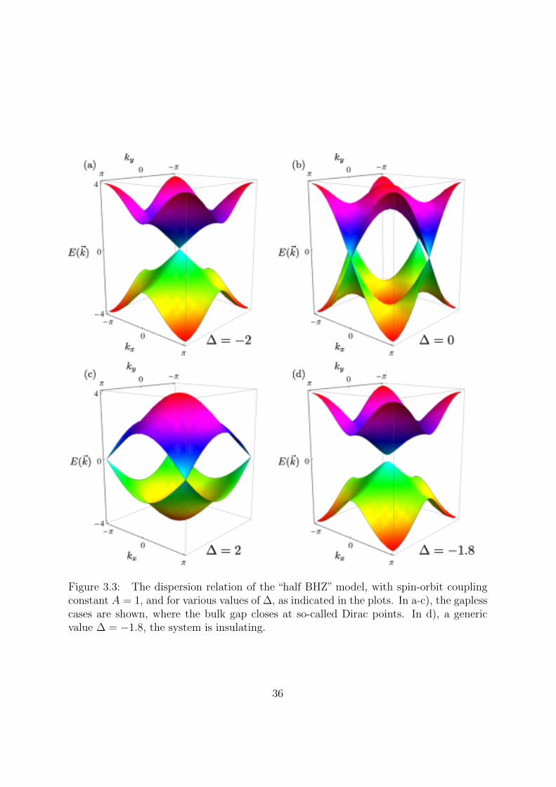
Figure 3.3: The dispersion relation of the “half BHZ” model, with spin-orbit couplingconstant A = 1, and for various values of ∆, as indicated in the plots. In a-c), the gaplesscases are shown, where the bulk gap closes at so-called Dirac points. In d), a genericvalue ∆ = −1.8, the system is insulating.
36
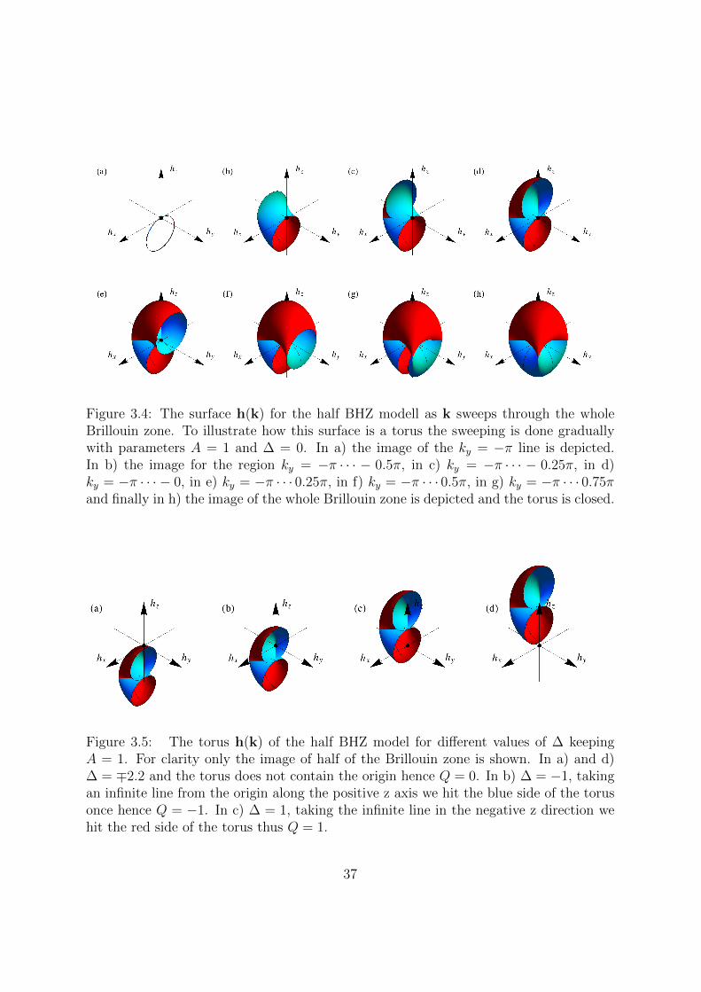
Figure 3.4: The surface h(k) for the half BHZ modell as k sweeps through the wholeBrillouin zone. To illustrate how this surface is a torus the sweeping is done graduallywith parameters A = 1 and ∆ = 0. In a) the image of the ky = −π line is depicted.In b) the image for the region ky = −π · · · − 0.5π, in c) ky = −π · · · − 0.25π, in d)ky = −π · · · − 0, in e) ky = −π · · · 0.25π, in f) ky = −π · · · 0.5π, in g) ky = −π · · · 0.75πand finally in h) the image of the whole Brillouin zone is depicted and the torus is closed.
Figure 3.5: The torus h(k) of the half BHZ model for different values of ∆ keepingA = 1. For clarity only the image of half of the Brillouin zone is shown. In a) and d)∆ = ∓2.2 and the torus does not contain the origin hence Q = 0. In b) ∆ = −1, takingan infinite line from the origin along the positive z axis we hit the blue side of the torusonce hence Q = −1. In c) ∆ = 1, taking the infinite line in the negative z direction wehit the red side of the torus thus Q = 1.
37
The boundary of the Brillouin zone is obtained by cutting the torus open: cutting italong two circles C1 and C2. The boundary means traversing along C1, then C2, then C1,but in the opposite direction, then along C2 in the opposite direction. The Berry vectorpotential A is a single-valued vector field on the torus. Its line integral then has to be 0.
This apparent paradox can be resolved by realizing that there must be a problem whenwe apply the Stokes’ theorem to get from Eq. (3.28) to Eq. (3.39). If A is smoothlydefined everywhere on the surface of the torus, the Chern number must indeed be 0.However, it can happen that A cannot be smooth over the whole Brillouin Zone. Thisis the case, if there is no choice of global gauge where the energy eigenstate |n, k〉 is asmooth function of k everywhere. As an example consider the two-level system.
A nonzero value of the Chern number shows that there is an obstruction towardsdefining a global, smooth energy eigenstate |n, k〉. The Chern number measures thenumber of vortices : points in k-space, for which the phase of |n, k〉 depends on thedirection of approach. For an infinitesimal circle around such a point, the phase of|n, k + dk〉 must wind at least once. If it winds more than once, we can with a gaugetransformation take the vortex apart to two singly charged vortices. If it does not wind,we can again with a gauge transformation get rid of the singularity. To read more on thispicture of the Chern number, see the paper of Kohmoto [9]. This picture of the Chernnumber as an obstruction also points towards the efficient way of numerically calculatingthe Chern number.
3.4.2 Efficient discretization of the Chern number
We follow the paper of Fukui, Hatsugai, and Suzuki [5] in the discussion.Above, we have seen that the Chern number reads
Q = − 1
2π
∫ ∫BZ
dkxdkyF (kx, ky); (3.40)
F (kx, ky) =∂Ay∂kx− ∂Ax∂ky
, (3.41)
using the notation of F for the Berry curvature. For brevity, we drop the index (n) wherethis leads to no confusion.
We now show how to efficiently discretize this integral on a momentum lattice:
k =2π
Nj, (3.42)
with j a 2D vector of integers. Assume we have in some gauge a set of eigenstates
|n(j)〉 . (3.43)
Even if there is no globally continuous gauge, these eigenstates only need to be welldefined on the lattice points, no problem with that.
38
Define as link variables the relative phase between eigenstates on neighbouring latticesites:
Uµ(j) =〈n(j + µ) | n(j)〉|〈n(j + µ) | n(j)〉|
; (3.44)
for
µ = x, y : x ≡ (1, 0); y ≡ (0, 1). (3.45)
For each plaquette, take the product of the relative phases around its boundary:
G(j) ≡ Ux(j)Uy(j + x)Ux(j + y)−1 Uy(j)−1. (3.46)
If instead of the vectors |n(j)〉 we had complex numbers α(j) on the sites, with theirrelative phases defining the link variables Uµ, this product would have to be 1. However,because of the extra “room” in the Hilbert space, the plaquette variable can have anyphase:
G(j) = eiF (j). (3.47)
Multiplying together all of the plaquette variables G(j), we get 1:
ΠjG(j) = 1. (3.48)
To prove this, consider multiplying the plaquette variables G together for two neighbour-ing plaquettes. The edge that they share cancels out from the product (See Fig. 3.6):
G(j)G(j + y) = Ux(j)Uy(j + x)Ux(j + y)−1 Uy(j)−1
Ux(j + y)Uy(j + y + x)Ux(j + 2y)−1 Uy(j + y)−1
= Ux(j)Uy(j + x)Uy(j)−1 Uy(j + y + x)Ux(j + 2y)−1 Uy(j + y)−1. (3.49)
When we calculate the product of all the plaquette variables on the full lattice all edgesare shared by two neighboring plaqettes, taking into account the periodic boundaryconditions. Therefore, from the product of the G for all plaquettes all edge contributionscancel: the product is 1.
Now concentrate on the plaquette variables F (j), which are the phases of the G(j).To properly define these phases, we have to select a branch for the logarithm:
F (j) ≡ i ln(Ux(j)Uy(j + x)Ux(j + y)−1 Uy(j)
−1)
; (3.50)
−π < F (j) ≤ π. (3.51)
If we sum the variables F (j) over all the plaquettes, do we get 0? No, for the above“cancellation of the edges” argument to go through, we would need to consider
F (j) ≡ i lnUx(j) + i lnUy(j + x)− i lnUx(j + y)− i lnUy(j) (3.52)
39

If −π ≤ F (j) < π, then it is equal to F (j). However, F can be outside that range: thenit is taken back into [−π, π) by adding an integer multiple of 2π. This happens when therelative phase around the loop, F (j), has a magnitude that is too big: i.e., when there isa vortex in plaquette j.
The discretized version of the Berry curvature counts the vortices by adding up theprojected variables F (j),
Q ≡ 1
2π
∑j
F (j). (3.53)
40
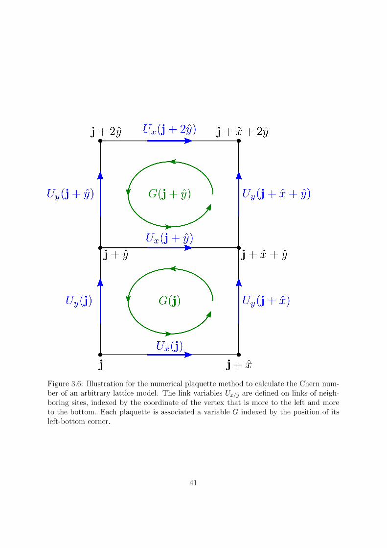
Figure 3.6: Illustration for the numerical plaquette method to calculate the Chern num-ber of an arbitrary lattice model. The link variables Ux/y are defined on links of neigh-boring sites, indexed by the coordinate of the vertex that is more to the left and moreto the bottom. Each plaquette is associated a variable G indexed by the position of itsleft-bottom corner.
41
Chapter 4
Edge states in half BHZ
The unique physical feature of topological insulators is the guaranteed existence of low-energy states at their boundaries. We have seen an example of this for a 1-dimensionaltopological insulator, the SSH model: A finite, open, “topologically nontrivial”SSH chainhosts 0 energy bound states at both ends. The “bulk–boundary correspondence” was theway in which the topological invariant of the bulk – in the case of the SSH chain, thewinding number of the bulk Hamiltonian – can be used to predict the number of edgestates.
For insulators of dimensions 2 and above, the edge states are not simple bound statesthat live at the edges of a finite sample, but consist of propagating modes. In this chapterwe show what these edge states are, how they arise for 2-dimensional insulators withbroken time-reversal symmetry. There can be any number N+ of counterclockwise andN− of clockwise propagating edge states in a single sample. We show that the differenceof these numbers, N+−N−, is a topological invariant, i.e., cannot change under adiabaticdeformations of the Hamiltonian, including those that introduce disorder at the edges ofthe sample. Moreover, this difference (or “signed sum”) of edge states is equal to the sumof the Chern numbers of the occupied (valence) bands of the translationally invariantbulk. This is the bulk–boundary correspondence for 2-dimensional “Chern insulators”.
4.1 Edge states
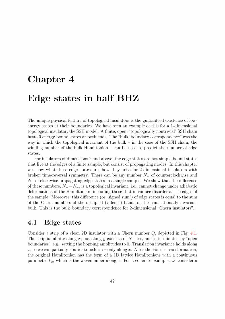
Consider a strip of a clean 2D insulator with a Chern number Q, depicted in Fig. 4.1.The strip is infinite along x, but along y consists of N sites, and is terminated by “openboundaries”, e.g., setting the hopping amplitudes to 0. Translation invariance holds alongx, so we can partially Fourier transform – only along x. After the Fourier transformation,the original Hamiltonian has the form of a 1D lattice Hamiltonians with a continuousparameter kx, which is the wavenumber along x. For a concrete example, we consider a
42
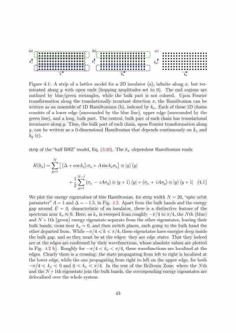
Figure 4.1: A strip of a lattice model for a 2D insulator (a), infinite along x, but ter-minated along y with open ends (hopping amplitudes set to 0). The end regions areoutlined by blue/green rectangles, while the bulk part is not colored. Upon Fouriertransformation along the translationally invariant direction x, the Hamiltonian can bewritten as an ensemble of 1D Hamiltonians (b), indexed by kx. Each of these 1D chainsconsists of a lower edge (surrounded by the blue line), upper edge (surrounded by thegreen line), and a long, bulk part. The central, bulk part of each chain has translationalinvariance along y. Thus, the bulk part of each chain, upon Fourier transformation alongy, can be written as a 0-dimensional Hamiltonian that depends continuously on kx andky (c).
strip of the “half BHZ” model, Eq. (3.30). The kx -dependent Hamiltonian reads
H(kx) =N∑y=1
[(∆ + cos kx)σz + A sin kxσx
]⊗ |y〉 〈y|
+1
2
N−1∑y=1
(σz − iAσy)⊗ |y + 1〉 〈y|+ (σz + iAσy)⊗ |y〉 〈y + 1| (4.1)
We plot the energy eigenvalues of this Hamiltonian, for strip width N = 20, “spin–orbitparameter”A = 1 and ∆ = −1.5, in Fig. 4.2. Apart from the bulk bands and the energygap around E = 0, characteristic of an insulator, there is a distinctive feature of thespectrum near kx ≈ 0. Here, as kx is sweeped from roughly −π/4 to π/4, the Nth (blue)and N + 1th (green) energy eigenstate separate from the other eigenstates, leaving theirbulk bands, cross near kx = 0, and then switch places, each going to the bulk band theother departed from. While −π/4 < k < π/4, these eigenstates have energies deep insidethe bulk gap, and so they must be at the edges: they are edge states. That they indeedare at the edges are confirmed by their wavefunctions, whose absolute values are plottedin Fig. 4.2 b). Roughly for −π/4 < kx < π/4, these wavefunctions are localized at theedges. Clearly there is a crossing: the state propagating from left to right is localized atthe lower edge, while the one propagating from right to left on the upper edge, for both−π/4 < kx < 0 and 0 < kx < π/4. In the rest of the Brillouin Zone, where the Nthand the N +1th eigenstate join the bulk bands, the corresponding energy eigenstates aredelocalized over the whole system.
43

Figure 4.2: Dispersion relation of a strip of half BHZ model, of width N = 20, “spin–orbitparameter”A = 1 and gap parameter ∆ = −1.5. Because the strip is translation invariantalong the edge, the wavenumber kx is a good quantum number, and the energy eigenvaluescan be plotted (left figure) as a function of kx, forming the dispersion relations. The twomiddle eigenvalues, the Nth and N + 1th, are plotted in blue (green), all other energyeigenvalues are in red. These two branches of the dispersion relation are special becausethey cross near kx = 0. In reality this is an avoided crossing with energy splitting ∝ e−N .The wavefunctions of the corresponding eigenstates are plotted as functions of kx andy in the plot to the right. Here blue (green) corresponds to the Nth (N + 1th) energyeigenstate, and the intensity at to the absolute value of the wavefunction at the givenposition. In the vicinity of the crossing, for −π/4 < k < π/4, the two middle eigenstateshave energies deep inside the bulk gap, and so their wavefunctions are concentrated atthe edges: they are edge states. For other momenta they delocalize over the whole chain.
44

4.2 Number of edge states as a topological invariant
The signed sum, N+−N−, of the number of edge states inside the gap on a single edge isa topological invariant. To understand what this statement means we explain the termsand provide illustrations using the half BHZ model. We identify an “edge state” as anenergy eigenstate whose wavefunction has over 90% of its weight within 3 unit cells of theedge. In Figs. 4.4–4.7, the energies of such states on the lower (upper) edge are markedby dark blue (green) dots. Since we want to talk about edge states on a single edge, e.g.the lower edge, we have to be careful to count only the blue branches of the dispersionrelation.
First, we clarify what we mean by the “number of edge states inside the gap”. Thebulk states of a 2D system form 2-dimensional bands. For a system with a “clean” edge,i.e., with translational invariance along the edge direction x, the edge states form 1-dimensional bands (wavenumber kx is a good quantum number). Pick an energy insidethe bulk gap; a convenient choice is E = 0, but any other energy value is equallygood. This defines a horizontal line in the graph of the dispersion relations. Pick anedge. Identify the number of times this line intersects the edge bands corresponding tothis edge (this number can also be 0). At each intersection, the group velocity of theedge band (dE/dkx) is either positive or negative: use this to assign +1 or −1 to theintersection. The number of intersections with positive group velocity is N+; the numberof those with negative group velocity is N−. The difference of these two numbers is the“net number of edge states inside the gap”.
The“net number of edge states inside the gap”, N+−N−, defined above is a topologicalinvariant, i.e., it is invariant under smooth changes of the Hamiltonian. This “topologicalprotection” is straightforward to prove, by considering processes that might change thisnumber.
The number of times edge state bands intersect E = 0 can change because newintersection points appear. These can form because an edge state band is deformed, andas a result of an adiabatic deformation of the system gradually develops a “bump”, localmaximum, and the local maximum gets displaced from E < 0 to E > 0. For a schematicexample, see Fig. 4.3 (a)-(c). Alternatively, the dispersion relation branch of the edgestate can also form a local minimum, gradually displaced from E > 0 to E < 0. In bothcases, the number of intersections of the edge band with the E = 0 line grows by 2, butthe two new intersections must have opposite group velocities. Therefore, both N+ andN− increase by 1, but their signed sum, N+ −N−, stays the same.
New intersection points can also arise because a new edge state band forms. As longas the bulk gap stays open, though, this new edge state band has to be a deformedversion of one of the bulk bands, as shown in Fig. 4.3 (a)-(h)-(i). Because the periodicboundary conditions must hold in the Brillouin Zone, the dispersion relation of the newedge state has to “come from” a bulk band and go back to the same bulk band, or itcan be detached from the bulk band, and be entirely inside the gap, but then its average
45

Figure 4.3: Adiabatic deformations of dispersion relations of edge states on one edge,in an energy window that is deep inside the bulk gap. Starting from a system with 3copropagating edge states (a), an edge state’s dispersion relation can develop a “bump”,(b)-(c). This can change the number of edge states at a given energy (intersections of thebranches with the horizontal line corresponding to the energy), but always by introducingnew edge states pairwise, with opposite directions of propagation. Thus the signed sumof edge states remains unchanged. Alternatively, two edge states can develop a crossing,that because of possible coupling between the edge states turns into an avoided crossing(d),(f). This cannot open a gap between branches of the dispersion relation (e), asthis would mean that the branches become multivalued functions of the wavenumber kx(indicating a discontinuity in E(kx), which is not possible for a system with short-rangehoppings). Therefore, the signed sum of edge states is also unchanged by this process.One might think the signed sum of edge states can change if an edge state’s directionof propagation changes under the adiabatic deformation, as in (g). However, this isalso not possible, as it would also make a branch of the dispersion relation multivalued.Deformation of the Hamiltonian can also form a new edge state dispersion branch, as in(a)-(h)-(i), but because of periodic boundary conditions along kx, this cannot change thesigned sum of the number of edge states.
46

group velocity is 0. In both cases, the above argument applies, and it has to intersectthe E = 0 line an even number of times, with 0 signed sum.
The number of times edge state bands intersect E = 0 can also decrease if two edgestate bands develop a gap. However, to open a gap, the edge states have to propagate indifferent directions: otherwise a crossing between edge states simply becomes an avoidedcrossing, but no gap is opened, see Fig. 4.3 d)-f). This same argument show why it isnot possible for an edge state to change its direction of propagation under an adiabaticdeformation without developing a local maximum or minimum (which cases we alreadyconsidered above). As shown in Fig. 4.3 (g), this would entail that at some stage duringthe deformation the edge state band was not single valued.
4.3 Numerical examples: the “half BHZ model”
We illustrate the ways translational invariant disorder (translational invariant along x)can affect edge states in the half BHZ model. First, we take the half BHZ model,Hamiltonian (4.1), and add disorder at the lower edge. The results are shown in Fig.4.4.Different types of disorder were used to deform the edge state bands, for details, see thefigure caption.
To show how disorder can open gaps in the edge state dispersion relations, we need asystem with more than one edge state. The most straightforward path to such a system,based, e.g., on the BHZ model, is layering sheets of Chern Insulators onto each other, asillustrated in Fig. 4.5. As an example, the Hamiltonian for a whole system of 3 layers isconstructed as
H2(kx) =
H(∆1, A1, kx) C 0C H(∆2, A2, kx − k2) C0 C H(∆3, A3, kx − k3)
(4.2)
The coupling between the layers is taken independent of position, Cmn = Cδmn.Numerical results for two and three coupled layers, with the Chern number of the
second layer +1 or −1, are shown in Figs. 4.6,4.7. The coupling of copropagating edgemodes lifts the degeneracies, but cannot open gaps in the spectrum. This is a simpleconsequence of the fact that an energy eigenstate has to be a single valued functionof momentum. To open a gap, counterpropagating edge states have to be coupled. Weachieve this by coupling layers of the BHZ model with opposite sign of the gap parameter∆. For the case of two layers (Fig. 4.6, second row), this opens a gap in the spectrum. Ifthere are three layers, there is a majority direction for the edge states, and so one edgestate survives the coupling.
47

Figure 4.4: Dispersion relation of a strip of half BHZ . Edge states, whose wavefunctionhas over 90% on the first/last 3 unit cells, are marked in dark blue/green. Top row:a strip with clean terminations, with ∆ = −1.2 (left), ∆ = 1.2 (middle), ∆ = 3.2(right). Bottom row: with the same parameters above, we added translation invariantdeformation to the edge region at y = 1. For the Chern insulators, this deformationis a long range hopping term (in this case, a 20th neighbor hopping term, ∝ cos20 kx),whereas for a trivial insulator, a simple onsite potential is used. The edge deformationsdo not affect the edge state at y ≈ N , nor the bulk states, but distorts the edge mode aty ≈ 1 and brings in new edge modes at energies that are in the bulk gap or above/belowall bulk energies. The deformation can change the number of edge states at a specificenergy, but only by adding a pair of edge states with opposite propagation directions.This leaves the topological invariant unchanged.
48
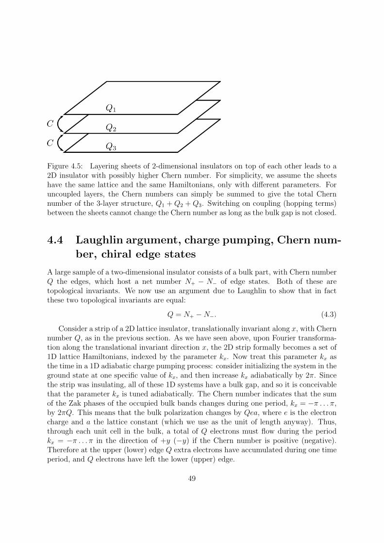
Figure 4.5: Layering sheets of 2-dimensional insulators on top of each other leads to a2D insulator with possibly higher Chern number. For simplicity, we assume the sheetshave the same lattice and the same Hamiltonians, only with different parameters. Foruncoupled layers, the Chern numbers can simply be summed to give the total Chernnumber of the 3-layer structure, Q1 + Q2 + Q3. Switching on coupling (hopping terms)between the sheets cannot change the Chern number as long as the bulk gap is not closed.
4.4 Laughlin argument, charge pumping, Chern num-
ber, chiral edge states
A large sample of a two-dimensional insulator consists of a bulk part, with Chern numberQ the edges, which host a net number N+ − N− of edge states. Both of these aretopological invariants. We now use an argument due to Laughlin to show that in factthese two topological invariants are equal:
Q = N+ −N−. (4.3)
Consider a strip of a 2D lattice insulator, translationally invariant along x, with Chernnumber Q, as in the previous section. As we have seen above, upon Fourier transforma-tion along the translational invariant direction x, the 2D strip formally becomes a set of1D lattice Hamiltonians, indexed by the parameter kx. Now treat this parameter kx asthe time in a 1D adiabatic charge pumping process: consider initializing the system in theground state at one specific value of kx, and then increase kx adiabatically by 2π. Sincethe strip was insulating, all of these 1D systems have a bulk gap, and so it is conceivablethat the parameter kx is tuned adiabatically. The Chern number indicates that the sumof the Zak phases of the occupied bulk bands changes during one period, kx = −π . . . π,by 2πQ. This means that the bulk polarization changes by Qea, where e is the electroncharge and a the lattice constant (which we use as the unit of length anyway). Thus,through each unit cell in the bulk, a total of Q electrons must flow during the periodkx = −π . . . π in the direction of +y (−y) if the Chern number is positive (negative).Therefore at the upper (lower) edge Q extra electrons have accumulated during one timeperiod, and Q electrons have left the lower (upper) edge.
49
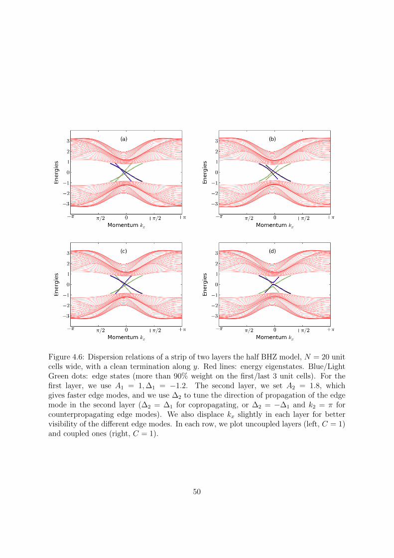
Figure 4.6: Dispersion relations of a strip of two layers the half BHZ model, N = 20 unitcells wide, with a clean termination along y. Red lines: energy eigenstates. Blue/LightGreen dots: edge states (more than 90% weight on the first/last 3 unit cells). For thefirst layer, we use A1 = 1,∆1 = −1.2. The second layer, we set A2 = 1.8, whichgives faster edge modes, and we use ∆2 to tune the direction of propagation of the edgemode in the second layer (∆2 = ∆1 for copropagating, or ∆2 = −∆1 and k2 = π forcounterpropagating edge modes). We also displace kx slightly in each layer for bettervisibility of the different edge modes. In each row, we plot uncoupled layers (left, C = 1)and coupled ones (right, C = 1).
50
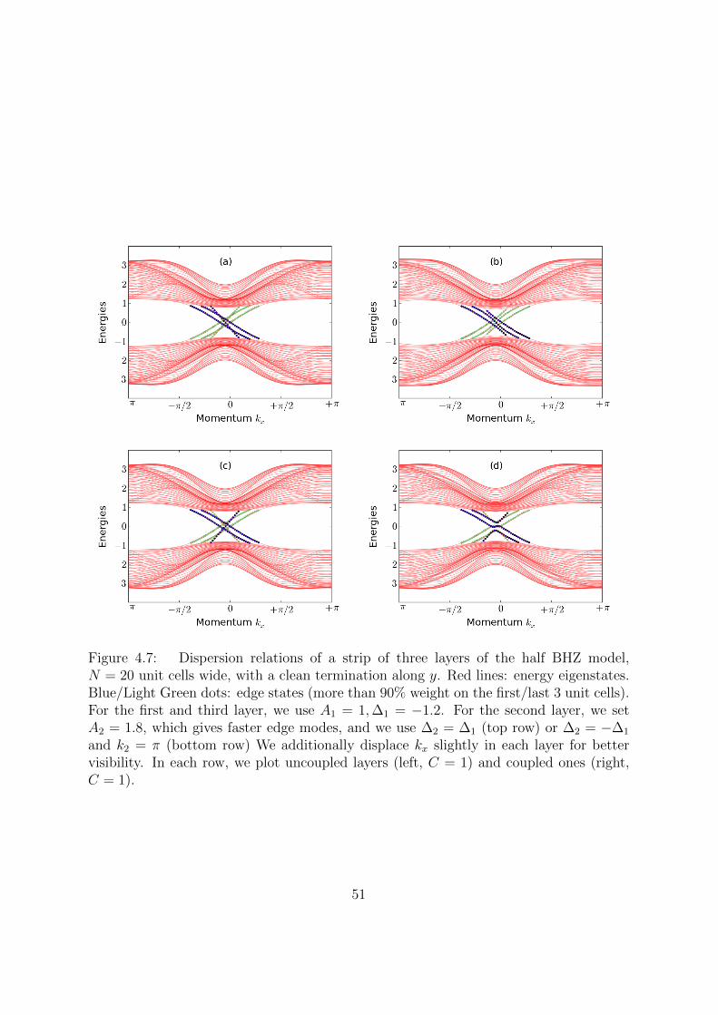
Figure 4.7: Dispersion relations of a strip of three layers of the half BHZ model,N = 20 unit cells wide, with a clean termination along y. Red lines: energy eigenstates.Blue/Light Green dots: edge states (more than 90% weight on the first/last 3 unit cells).For the first and third layer, we use A1 = 1,∆1 = −1.2. For the second layer, we setA2 = 1.8, which gives faster edge modes, and we use ∆2 = ∆1 (top row) or ∆2 = −∆1
and k2 = π (bottom row) We additionally displace kx slightly in each layer for bettervisibility. In each row, we plot uncoupled layers (left, C = 1) and coupled ones (right,C = 1).
51
The only way this electron pumping can occur is if, at the end of the pumping cycle,the system is not in the ground state any more. At the end of the cycle, a number |Q|of states with negative energy at the lower (upper) edge will be empty, and the samenumber of states with positive energy at the upper (lower) edge will be occupied. Weremark that although these states are assigned to the upper or the lower edge, theirenergies are not necessarily in the bulk gap, and so their wavefunctions can extend farinto the bulk.
Since the pump cycle was adiabatic, the energies of all states change continuously asthe parameter kx is tuned from −π to π. Thus, there have to be |Q| branches of thedispersion relation with positive (negative) group velocity inside the gap at the upperedge, and |Q| branches with negative (positive) group velocity inside the gap at the loweredge, if the Chern number Q of the bulk is positive (negative). Each of these branchesof the dispersion relation correspond to an edge state.
This completes the proof: the magnitude of the Chern number of the bulk of a 2Dlattice system gives the number of edge states at the edges of the system. The sign of theChern number gives the direction of propagation of these edge states. These are chiralstates: at any edge, all of these propagate in the same direction. Since their energy is inthe bulk gap, their wavefunctions decay exponentially away from the edge towards thebulk.
4.5 Robustness of edge states
Up to now, we have considered clean edges, i.e., 2D Chern Insulators that were terminatedby an edge (at y = 0 and y = N), but translationally invariant along the edge, alongx. This translational invariance, and the resulting fact that the wavenumber kx is agood quantum number, was used for the definition of the topological invariant N+−N−,which was the net number of edge bands propagating along the edge, equal to the bulkChern number, Q. With disorder in the edge region that breaks translational invariancealong x, we no longer have a good quantum number kx, and edge state bands are notstraightforward to define. However, as we show in this section, the edge states must stillbe there in the presence of disorder, since disorder at the edges cannot close the bulkgap.
Consider a finite, sample of a Chern insulator, with a clean bulk part but disorderededge region, as depicted in Fig. 4.8. The bulk gap of the sample decreases due to disorder,but we suppose that it is not closed completely (just renormalized). Consider now a smallpart of the sample, containing some of the edge, indicated by the dotted rectangle on theright of Fig. 4.8. Although this is much smaller than the whole sample, it is big enoughso that part of it can be considered as translation invariant “bulk”. Now in this smallpart of the sample, we adiabatically (and smoothly) deform the Hamiltonian in such away that we set the disorder gradually to 0. This includes straightening the part of the
52
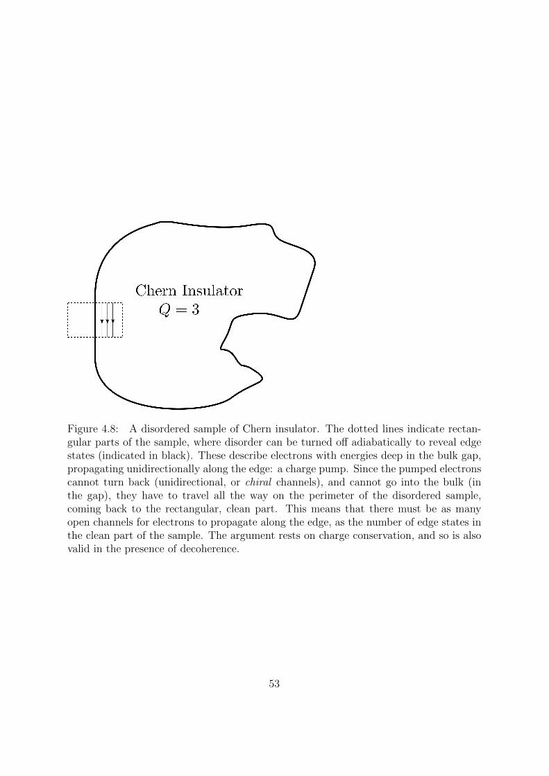
Figure 4.8: A disordered sample of Chern insulator. The dotted lines indicate rectan-gular parts of the sample, where disorder can be turned off adiabatically to reveal edgestates (indicated in black). These describe electrons with energies deep in the bulk gap,propagating unidirectionally along the edge: a charge pump. Since the pumped electronscannot turn back (unidirectional, or chiral channels), and cannot go into the bulk (inthe gap), they have to travel all the way on the perimeter of the disordered sample,coming back to the rectangular, clean part. This means that there must be as manyopen channels for electrons to propagate along the edge, as the number of edge states inthe clean part of the sample. The argument rests on charge conservation, and so is alsovalid in the presence of decoherence.
53
open boundary of the sample that falls into the dotted rectangle, to a straight line. Thedeformation is adiabatic in the sense that the bulk gap is not closed in the process. Sincethis small part is a clean Chern insulator, with a bulk Chern number of Q, it can bedeformed in such a way that the only edge states it contains are |Q| states propagatingcounterclockwise (if Q > 0, say).
Consider an electron in an edge state in the small clean part of the sample, withenergy deep inside the bulk gap (E ≈ 0). What can its future be, as its time evolutionfollows the Schrodinger equation appropriate for this closed system? Since the edgestate is a chiral mode, the electron has to propagate along the edge until it leaves theclean region. Because of unitarity, the electron cannot “stop” at the edge: that wouldmean that at the “stopping point”, the divergence of the particle current in the energyeigenstate is nonzero. In other words, the particle current that flows in the edge statehas to flow somewhere. (Put differently, if the mode describing an edge state electron“stopped at the interface”, two electrons, initially orthogonal, following each other in themode, would after some time arrive to the same final state. This would break unitarity.)After leaving the clean part of the sample, the electron cannot propagate into the bulk,since its energy is deep in the bulk gap. The disorder in the clean part was removedadiabatically, and thus there are no edge states at the interface of the clean part and thedisordered part of the sample, along the dashed line. The electron cannot turn back, asthere are no edge states running “down” along the edge in the clean part. The only thingthe electron can do is propagate along the edge, doing a full loop around the sample untilit comes back to the clean part from below again.
The argument of the previous paragraph shows that even though the sample is dis-ordered, there has to be a low energy mode that conducts perfectly (reflectionless) alongthe edge. Since at 0 energy there are Q orthogonal states an electron can be in at theedge of the clean part of the sample, unitarity of the dynamics of the electrons requiresthat all along the edge of the disordered sample there are Q orthogonal modes that con-duct counterclockwise. There can be additional low energy states, representing trappedelectrons, or an equal number of extra edge states for electrons propagating counter-clockwise and clockwise. However, the total number of counterclockwise propagatingedge modes at any part of the edge always has to be larger by Q than the number ofclockwise propagating edge modes. Because the Hamiltonian is short range, our conclu-sions regarding the number of edge states at any point far from the deformed region haveto hold independent of the deformation.
To be precise, in the argument above we have shown the existence of Q edge states allalong the edge of the sample, except for the small part that was adiabatically cleaned fromdisorder. One way to finish the argument is by considering another part of the sample.If we now remove the disorder adiabatically only in this part, we obtain the existence ofthe edge modes in parts of the sample including the original dotted rectangle, which wasnot covered by the argument of the previous paragraph.
54
Chapter 5
Edge states in the 2D Dirac equation
The appearance of edge states in the half BHZ lattice model was discussed in the pre-ceding Chapter. There, the edge states were revealed and analyzed via numerical diag-onalization of the Hamiltonian of a terminated lattice. Here, we argue that it is alsopossible to describe these states in terms of a partial differential equation (PDE) similarto the Schrodinger and the Dirac equation. Working with a PDE instead of a latticemodel offers the potential advantage of obtaining analytical results for certain physicalproperties of the considered material. Here we derive the Schrodinger-type PDE thatprovides a low-energy continuum description of the half BHZ lattice model, and use it toanalytically characterize the edge states appearing at boundaries between regions withdifferent Chern numbers, without the need to numerically diagonalize large tight-bindingHamiltonians. Even though in the entire Chapter we build our discussion on the halfBHZ model, the applicability of the technique introduced here, called envelope functionapproximation (EFA), is more general and widely used to describe electronic states invarious crystalline solids [1].
5.1 Reminder: the half BHZ model
The k-space Hamiltonian of the half BHZ model was defined in Eq. (3.30):
H(kx, ky) = (∆ + cos kx + cos ky)σz + A(sin kxσx + sin kyσy) = h(k) · σ, (5.1)
with
h(k) =
A sin kxA sin ky
∆ + cos kx + cos ky
. (5.2)
The corresponding dispersion relation is
E±(k) = ±h(k) ≡ ±|h(k)|. (5.3)
55
The half BHZ model describes an insulator if ∆ is not equal to -2, 0 or 2. The Chernnumber Q of the half BHZ insulator can take on three different values, determined bythe single parameter ∆:
Q =
0, if 2 < ∆,+1 if 0 < ∆ < 2,−1 if − 2 < ∆ < 0,0 if ∆ < −2
. (5.4)
The number and propagation direction of topologically protected edge states at a domainwall is determined by the magnitude and difference of the Chern numbers of the twodomains, respectively.
5.2 2D Dirac equation as a low-energy effective model
5.2.1 Gapless spectrum in the half BHZ model
First, consider the cases when the half BHZ model is metallic, ie, when its spectrum hasno energy gap. This is the case if and only if ∆ equals -2, 0 or 2. The correspondingband structures with A = 1 are shown in Fig. 3.3a, b and c. For ∆ = −2, the two bandstouch at k = (0, 0), and form a conically shaped dispersion relation in the vicinity of thatpoint, see Fig. 3.3a. For ∆ = 0 there are two inequivalent touching points at k = (0, π)and k = (π, 0). Fig. 3.3 shows four of them, though note that k = (−π, 0) is equivalentto (π, 0) and k = (0,−π) is equivalent to k = (0, π). For ∆ = 2 there is a single touchingpoint at k = (π, π). The other three touching points seen in Fig. 3.3c are equivalent with(π, π).
The points where the bands touch are called Dirac points, and the conically shapedparts of the bands are called Dirac cones. The Dirac points and the Dirac cones are alsoreferred to as valleys, or as Dirac valleys.
To describe low-energy excitations just above the filled valence band in such a con-ductor, it is sufficient to use a linearized approximation of the half BHZ HamiltonianH(k) that is obtained via a Taylor expansion of H(k) up to first order in the k-spacelocation q = k−kD measured from the Dirac point kD. For example, in the case ∆ = −2and correspondingly, kD = (0, 0), the linearized Hamiltonian reads
H(kD + q) ≈ A(qxσx + qyσy) (5.5)
The dispersion relation is E±(q) = ±Aq, which equals the dispersion relation obtainedafter linearizing Eq. (5.3) around kD. Note that the dispersion relation of the Diracequation of fermions with zero mass is
E±(k) = ±~kc, (5.6)
56

where ~ is the reduced Planck’s constant and c is the speed of light. Therefore, theparameter A of the half BHZ model plays the role of ~c of the relativistic dispersionrelation (5.6). The eigenstates of the linearized Hamiltonian are
ψ±(q) =1√2
(1±eiϕ
), (5.7)
where ϕ is the azimuthal angle of the wave vector q. i.e., ϕ = arctan qyqz
.Note that at this point, the linearization of the Hamiltonian does not seem to be a
particularly fruitful simplification: to obtain the dispersion relation and the eigenstates,a 2 × 2 matrix has to be diagonalized, no matter if the linearization has been done ornot. However, linearizing the Hamiltonian is the first step towards a simple continuumdescription of inhomogeneous lattices, as shown below.
5.2.2 Opening a gap
Now consider a half BHZ insulator that is close to being metallic, ie, ∆ ≈ ∆0 where ∆0
is either -2, 0 or 2. To be specific, we consider the example where ∆0 = −2 and thecorresponding Dirac point is at the Brillouin zone center, kD = (0, 0). The dispersionrelation for ∆ = −1.8 is shown in Fig. 3.3d. In the vicinity of the metallic state, as seenin the figure, a small gap equal to the energy splitting of the two states at the Diracpoint kD = (0, 0), opens in the spectrum.
The states and the dispersion relation around kD can again be described by a lin-earized approximation of the half BHZ Hamiltonian H(k) that is obtained via a Taylorexpansion of H(k) up to first order in the k-space location q = k−kD measured from theDirac point kD. For example, in the case of ∆0 = −2 and kD = (0, 0), the linearizationyields
H(kD + q) ≈Mσz + A (qxσx + qyσy) , (5.8)
where we defined M = ∆−∆0. The dispersion relation reads
E±(q) = ±√M2 + A2q2. (5.9)
Note that the dispersion relation of the Dirac equation for fermions with finite massµ 6= 0 reads
E±(k) = ±√µ2c4 + ~2k2c2. (5.10)
Therefore, the parameter M of the half BHZ model plays the role of µc2 of the relativisticdispersion relation (5.10). The (unnormalized) eigenstates of the linearized Hamiltonian(5.8) have the form
ψ±(q) =
(qx − iqyE± −M
). (5.11)
57

5.2.3 Inhomogeneous systems
A half BHZ lattice with inhomogeneous ∆ parameter might support topologically pro-tected bound states at boundaries separating locally homogeneous regions with differentChern numbers. Under certain conditions, as shown below, these bound states can bedescribed analytically using the envelope function approximation (EFA) that results ina low-energy continuum description, i.e., a partial differential equation similar to theDirac equation, of the states of the lattice. EFA is based on the assumption that thelow-energy eigenstates of the inhomogeneous system are localized in Fourier space to theclose neighborhood of a given wave vector. In the rest of this Chapter, we focus on thecase where the inhomogeneous ∆ is in the vicinity of −2 (e.g., |∆+2| 1), in which casethe the low-energy excitations are expected to localize in Fourier space around the bandextremum point kD = (0, 0) (see Figs. 3.3a and d). Here we derive the Schrodinger-typePDE, in fact resembling the two-dimensional Dirac equation, relevant for this case, andin the next Section we solve that for simple domain-wall arrangements.
The considered lattice is inhomogeneous due to the spatial dependence of the pa-rameter ∆. In the tight-binding lattice model, we denote the value of ∆ on site m =(mx,my) as ∆m, and correspondingly, we introduce the local mass parameter on site mas Mm = ∆m − (−2) = ∆m + 2. The main result of the EFA in our case is that theeigenstates and eigenvalues of the continuum Hamiltonian
HEFA = M(r)σz + A (qxσx + qyσy) , (5.12)
which we will refer to as the EFA Hamiltonian, correspond to and determine the low-energy eigenstates and eigenvalues of the tight-binding Hamiltonian of the inhomoge-neous lattice model. In (5.12), M(r) is a smooth extension of Mm such that M(rm) =Mm, and qα is the differential operator −i∂α. Note that HEFA is related to the linearizedk-space Hamiltonian (5.8) by the relations M ↔ M(r) and qα ↔ qα. The eigenvalueequation
HEFAψ(r) = Eψ(r). (5.13)
will be referred to as the EFA Schrodinger equation and we call ψ(r) the envelope func-tion. Note that in the case considered here, the EFA Schrodinger equation (5.13) takesthe form of a 2D Dirac equation with inhomogeneous mass.
Before specifying the connection between HEFA and the inhomogeneous tight-bindingmodel, a rather informal definition of spatially slowly varying functions is in order. Wewill call the envelope function ψ(r) spatially slowly varying on the scale of the latticeconstant (‘ssv’ for short), if its Fourier-transform ψF (q) is localized to the |q| π region,i.e., to the vicinity of the center of the first Brillouin zone of the lattice.
With this definition at hand, we can formulate the EFA proposition. Consideran inhomogeneous half-BHZ lattice with spatially varying mass parameter Mm, with|Mm| 1 as discussed above. The Hamiltonian of the lattice is H =
∑`,`′ H`,`′a
†`a`′ ,
58

where ` = (m, j) ≡ (mx,my, j) is a composite index of the two-component unit cell index
m = (mx,my) and internal (spin) quantum number j ∈ ↑, ↓, and a†` creates an electronon site m with spin quantum number j. The matrix elements H`,`′ are given in Eq. (3.35).Assume that the pair (ψ(r), E) solves the EFA Schrodinger equation corresponding tothis lattice and ψ(r) is ssv. Define the tight-binding state |Ψ〉 =
∑`=(m,j) ψj(rm)a†` |0〉.
It is claimed that the tight-binding state |Ψ〉 is approximately an eigenstate of the inho-mogeneous lattice Hamiltonian with the eigenvalue E: H |Ψ〉 = E |Ψ〉.
To prove this, we calculate H |Ψ〉:
H |Ψ〉 =
(∑`,`′
H`,`′ a†`a`′
)(∑`′′
ψj′′(rm′′)a†`′′ |0〉
)=∑`,`′
H`,`′ψj′′(rm′′)a†` |0〉 , (5.14)
which, after separating H to a spatially depenent on-site part U`,`′ = ∆mδm,m′ (σz)j,j′and a spatially homogeneous hopping part T`,`′ = H`,`′ − U`,`′ reads
H |Ψ〉 =∑`,`′
(U`,`′ + T`,`′)ψj′(rm′) |`〉 . (5.15)
Here we introduced the notation |`〉 = a†` |0〉.Consider the hopping part of (5.15) first:∑
`,`′
T`,`′ψj′(rm′) |`〉 =∑`,`′
T`,`′
(∫dqψFj′ (q)eiqrm′
)|`〉 =
∑`,j′
∫dqTj,j′(q)ψFj′ (q)eiqrm |`〉 .
(5.16)In the first step we inserted the Fourier transform ψF (q) of the envelope function ψ(r),and in the second we utilized the fact that T is representing a homogeneous latticeHamiltonian and therefore
∑`′ T`,`′ψj′(q)eiqrm′ = eiqrm
∑j′ Tj,j′(q)ψj′(q). Note that the
explicit form of T (q) is T (q) = (cos qx + cos qy)σz + A(sin qxσx + sin qyσy) in our case,see Eq. (5.1).
We now make use of the assumption that ψ(r) is ssv, which implies that the integrandof the q-integral in the last formula of (5.16) is significant only around q = 0. Thereforewe can expand T (q) around q = 0, yielding the following approximation:∑
`,`′
T`,`′ψj′(rm′) |`〉 ≈∑`,j′
∫dq[Tj,j′(q = 0) + (∇qTj,j′)q=0 · q
]ψFj′ (q)eiqrm |`〉 . (5.17)
As the next step, we use qαeiqrm = (−i∂αeiqr)r=rm
= (qαeiqr)r=rm
, which implies thatthe second factor (q) of the second term in the square bracket of Eq. (5.17) can besubstituted with q . Therefore∑
`,`′
T`,`′ψj′(rm′) |`〉 ≈∑`
[∫dqA (qxσx + qyσy) ψ
F (q)eiqr]j,r=rm
|`〉
=∑`
[A (qxσx + qyσy) ψ(r)]j,r=rm|`〉 . (5.18)
59
Together with the on-site U terms of Eq. (5.15) we have
H |Ψ〉 ≈∑`
[M(r)σz + A (qxσx + qyσy)]ψ(r)j,r=rm|`〉 , (5.19)
which, as ψ(r) solves the EFA Schrodinger equation with energy E, equals
H |Ψ〉 ≈∑`
Eψj(rm) |`〉 = E |Ψ〉 . (5.20)
With this the proof is concluded.Even though this proposition was stated for the special case of the half BHZ model
with ∆(rm) ≈ −2, it can be straightforwardly generalized to the other two nearly metallicstates of the half BHZ model (∆(rm) ≈ 0 and ∆(rm) ≈ 2), as well as to describe electronicstates in the vicinity of a band extremum in a generic crystalline solid. In fact, EFA isa widely used method to describe such electronic states in the presence of a spatiallyslowly varying electromagnetic field.
Finally, let us highlight a limitation of the EFA that perhaps is not obvious from theabove statement. Even though there was no explicit condition on the characteristics ofthe mass inhomogeneity in the EFA proposition above, the ssv condition on the enve-lope function ψ(r) is actually an implicit condition for the inhomogeneous mass M(rm).Namely, if the Fourier components of the spatial mass inhomogeneity that correspondto wave vectors outside the central part of the Brillouin zone are strong enough, thenthe low-energy solutions of the EFA Schrodinger equation acquire large-q Fourier com-ponents, and therefore cannot fulfill the ssv criterion. Therefore, the applicability ofthe EFA scheme is limited to inhomogeneities that are also, in a certain sense, spatiallyslowly varying.
5.3 Edge states
Having the EFA Hamiltonian (5.12) at hand, we can now use it to describe low-energystates in the inhomogeneous half BHZ model, provided |M(x, y)| 1 everywhere in thex-y plane. From now on, we measure the prefactors in the EFA Hamiltonian in units ofA, hence the Dirac-type EFA Schrodinger equation reads:
[M(x, y)σz + σxqx + σy qy]ψ(x, y) = Eψ(x, y). (5.21)
Consider the homogeneous case first: M(x, y) = M0, where M0 might be positive ornegative. What is the dispersion relation for propagating waves? What are the energyeigenstates? The answers follow from the plane-wave Ansatz
ψ(x, y) =
(ab
)eiqxxeiqyy (5.22)
60
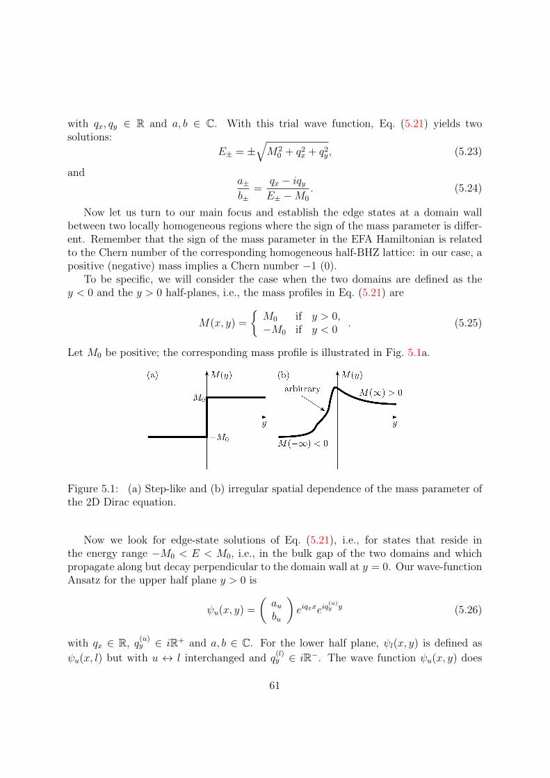
with qx, qy ∈ R and a, b ∈ C. With this trial wave function, Eq. (5.21) yields twosolutions:
E± = ±√M2
0 + q2x + q2
y, (5.23)
anda±b±
=qx − iqyE± −M0
. (5.24)
Now let us turn to our main focus and establish the edge states at a domain wallbetween two locally homogeneous regions where the sign of the mass parameter is differ-ent. Remember that the sign of the mass parameter in the EFA Hamiltonian is relatedto the Chern number of the corresponding homogeneous half-BHZ lattice: in our case, apositive (negative) mass implies a Chern number −1 (0).
To be specific, we will consider the case when the two domains are defined as they < 0 and the y > 0 half-planes, i.e., the mass profiles in Eq. (5.21) are
M(x, y) =
M0 if y > 0,−M0 if y < 0
. (5.25)
Let M0 be positive; the corresponding mass profile is illustrated in Fig. 5.1a.
Figure 5.1: (a) Step-like and (b) irregular spatial dependence of the mass parameter ofthe 2D Dirac equation.
Now we look for edge-state solutions of Eq. (5.21), i.e., for states that reside inthe energy range −M0 < E < M0, i.e., in the bulk gap of the two domains and whichpropagate along but decay perpendicular to the domain wall at y = 0. Our wave-functionAnsatz for the upper half plane y > 0 is
ψu(x, y) =
(aubu
)eiqxxeiq
(u)y y (5.26)
with qx ∈ R, q(u)y ∈ iR+ and a, b ∈ C. For the lower half plane, ψl(x, y) is defined as
ψu(x, l) but with u ↔ l interchanged and q(l)y ∈ iR−. The wave function ψu(x, y) does
61
solve the 2D Dirac equation defined by Eqs. (5.21) and (5.25) in the upper half planey > 0 provided
q(u)y = iκ ≡ i
√M2
0 + q2x − E2 (5.27)
andaubu
=qx + κ
E −M0
(5.28)
Similar conditions apply for the ansatz ψl(x, y) for the lower half plane, with the substi-tutions u 7→ l, κ 7→ −κ and M0 7→ −M0. The complete (unnormalized) wave functionhas the form
ψ(x, y) = ψu(x, y)Θ(y) + cψl(x, y)Θ(−y), (5.29)
where c is a yet unknown complex parameter to be determined from the boundaryconditions at the domain wall.
The wave function (5.29) is an eigenstate of the EFA Hamiltonian with energy E ifthe boundary condition that the wave function is continuous on the line y = 0, that is,
ψu(x, 0) = ψl(x, 0), (5.30)
is fulfilled for every x. Note that in our case, the Dirac equation is a first-order differentialequation and therefore there is no boundary condition imposed on the derivative of thewave function.
The boundary condition (5.30) determines the value of the parameter c as well as thedispersion relation E(qx) of the edge states. First, (5.30) implies
qx − κ = c(qx + κ) ⇒ c =qx − κqx + κ
, (5.31)
E +M0 = c(E −M0) ⇒ −qxM0 = κE. (5.32)
Note that κ depends on E according to Eq. (5.27). It is straigthforward to find thedispersion relation of the edge states by solving −qxM0 = κ(E)E for E with the condition−M0 < E < M0:
E = −qx. (5.33)
This simple dispersion relation is shown in Fig. 5.2a. Together with Eq. (5.27), thisdispersion implies that the localization length of edge states is governed by M0 only, i.e.,is independent of qx. The squared wave function of an edge state is shown in Fig. 5.2b.
A remarkable consequence of this simple dispersion relation is that the spinor com-ponents of the envelope function also have a simple form:(
aubu
)=
(albl
)=
(1−1
). (5.34)
Edge states at similar mass domain walls at ∆(y) ≈ 0 and ∆(y) ≈ 2 can be derivedanalogously. Note that at ∆(y) ≈ 0, the low-energy states can reside in two different
62

Figure 5.2: Edge state obtained from the 2D Dirac equation. (a) Dispersion relation and(b) squared wave function of an edge state localized at the mass domain wall illustratedin Fig. 5.1a.
Dirac valleys, around kD = (0, π) or kD = (π, 0), and there is one edge state in each valley.The number of edge states obtained in the continuum model, as well as their directionsof propagation, are in correspondence with those obtained in the lattice model; as wehave seen for the latter case, the number and direction are given by the magnitude andthe sign of Chern-number difference across the domain wall, respectively.
An interesting fact is that the existence of the edge state is not constrained to case ofa sharp, step-like domain wall described above. Moreover, the simple dispersion relationand spinor structure found above generalize for more irregular domain walls. To see this,consider an almost arbitrary 1D spatial dependence of the mass, illustrated in Fig. 5.1b:M(x, y) = M(y) with the only condition that M changes sign between the half-planesy < 0 and y > 0, i.e., M(y → −∞) < 0 and M(y →∞) > 0. We claim that there existsa solution of the corresponding 2D Dirac equation that propagates along the domainwall, has the dispersion relation E = −qx, is confined in the direction perpendicular tothe domain wall, and has the wave function
ψ(x, y) =
(1−1
)eiqxxf(y). (5.35)
To prove this proposition, insert this wave function ψ(x, y) to the 2D Dirac equation andsubstitute E with −qx therein. This procedure results in two equivalent equations thatare fulfilled if ∂yf(y) = −M(y)f(y), implying that Eq. (5.35) is indeed a normalizablesolution with E = −qx provided that the function f has the form
f(y) = e−∫ y0 dy
′M(y′). (5.36)
63
In the preceding Chapters, we introduced the topological characterization of latticemodels and the corresponding edge states, with the Brillouin zone of the lattice playinga central role in the formulation. In this Chapter, we demonstrated that under certainconditions, a low-energy continuum description (the EFA Schrodinger equation) can bederived from a lattice model, and can be used to describe edge states at domain wallsbetween regions of differing topological character. Besides being a convenient analyt-ical tool to describe inhomogeneous lattices, the envelope-function approximation alsodemonstrates that the emergence of protected edge states is not restricted to latticemodels.
64
Chapter 6
2-dimensional time-reversalinvariant topological insulators
In the previous chapters, we have understood how 2-dimensional insulators can host chi-ral (i.e., one-way propagating) edge states. The existence of chiral edge states precludestime-reversal symmetry. Indeed, time-reversed edge states would describe particles prop-agating backwards along the edge. In “Chern insulators”, the fact that these states arenot present in the spectrum is what ensures the reflectionless propagation of particles atthe edges.
What about time-reversal symmetric (or time-reversal invariant, TRI) two-dimensionalinsulators? According to the above, they cannot be Chern insulators. Interestinglythough, the same time-reversal symmetry that ensures that for every edge state there isa “backward-propagating” partner, can also ensure that no scattering between these twomodes occurs. This means that it is possible for time-reversal invariant 2D insulators tohost edge states that show reflectionless propagation, in both directions, at both edges.The details of why and how this happens are discussed in this and the following chapters.
We will find that all two-dimensional time-reversal invariant insulators fall into twoclasses: the trivial class, with an even number of pairs of edge states at a single edge,and the topological class, with an odd number of pairs of edge states at a single edge.We then subsequently show that disorder that breaks translational invariance along theedge can destroy edge state conduction in the trivial class, but not in the topologicalclass.
For Chern Insulators, we had a simple way to relate the topological invariant charac-terizing the properties of the edge of a finite sample, the net number of edge states on theedge, N+ −N−, to a topological invariant characterizing the translation invariant bulk,the Chern number Q. We showed that Q = N+−N− using the Laughlin argument, whichmapped the 2-dimensional system to a periodically, adiabatically pumped 1-dimensionalchain. After the mapping, the unit of charge pumped through the chain during a periodcould be identified with the net number of chiral edge states. This is the bulk–boundary
65
correspondence for Chern insulators.Unfortunately, identifying and calculating the bulk topological invariant of a time-
reversal invariant two-dimensional insulator is much more cumbersome than for a Cherninsulator. There is extensive mathematical work on how to formulate the bulk invariant,but there is no general and simple recipe for actually calculating it for a lattice model.Therefore, in this chapter we only give some of the theoretical elements used in theconstructions, and the numerical recipe for the special (but rather common) case ofsystems with inversion symmetry.
6.1 Time-Reversal Symmetry
Before we discuss Time-reversal symmetric topological insulators, we first need to under-stand what we mean by time reversal symmetry, and how it leads to Kramers’ degeneracy.
6.1.1 Time Reversal in continuous variable quantum mechanics
Take a single particle with time independent Hamiltonian H = (p−eA(r))2+V (r), whereA and V are the vector and scalar potentials, real valued functions of r, respectively,and e is the charge of the particle. The corresponding Schrodinger equation for thewavefuncion Ψ(r, t) reads
i∂tΨ(r, t) =
(−i∂r − eA(r))2 + V (r)
Ψ(r, t). (6.1)
Any solution Ψ of the above equation can be complex conjugated, and gives a solutionof the complex conjugate of the Schrodinger equation,
−i∂tΨ(r, t)∗ =
(−i∂r + eA(r))2 + V (r)
Ψ(r, t)∗. (6.2)
We use K to denote the operator that complex conjugates everything to its right in realspace basis. Note that K2 = 1, and therefore, KAK = A∗, where A is any operator orvector, and ∗ denotes complex conjugation in real space basis. The Schrodinger equationabove can thus be written succintly as
Ki∂tΨ = Ki∂tKKΨ = −i∂tΨ∗ = KHKKΨ = H∗Ψ∗. (6.3)
The above relation shows that for any closed quantum mechanical system, there is asimple way to implement time reversal. This requires to change both the wavefunctionΨ to Ψ∗ and the Hamiltonian H to H∗.
In the special case where the Hamiltonian in real space basis is real, H∗ = H, we canimplement time reversal by only acting on the wavefunction. In that case, we say thatthe system has time reversal symmetry. For the scalar Schrodinger equation above, thishappens if there is no vector potential, A = 0. To see this more explicitly, consider time
66
evolution for a time t, then applying the antiunitary operator K, then continuing timeevolution for time t, then applying K once more:
U = Ke−iHtKe−iHt = e−KiHtKe−iHt = eiH∗te−iHt (6.4)
If H∗ = H, then U = 1, which means that K acts like time reversal.Time reversal is an operation that is local in space, that takes x→ x and p→ −p.
6.1.2 Two types of time reversal
For a particle with an internal degree of freedom, time reversal T can also include aunitary rotation of this internal degree of freedom:
T = τK, (6.5)
where τ is a unitary operator. For complex conjugation K to be well defined we alsohave to fix the internal basis on which it acts. For example, for a spin-1/2 particle, timereversal should also flip the spin, which is achieved by T = −iσyK, if K is defined on thebasis of the eigenstates of σz. The fact that this works can be checked by T σjT −1 = −σjfor j = x, y, z.
A simple requirement for a time reversal operator is that if squared, it should give atmost a phase, eiφ:
τKτK = ττ ∗ = eiφ. (6.6)
This phase turns out to have only two possible values: 0 or π. Multiplying Eq. (6.6) fromthe left by τ †, we get τ ∗ = eiφτ † = eiφ(τ ∗)T , where T denotes transposition. Iteratingthis last relation once more, we obtain τ ∗ = e2iφτ ∗, which means eiφ = ±1, wherefore
T 2 = ±1. (6.7)
6.1.3 T 2 = −1 gives Kramers’ degeneracy
Time reversal T is an antiunitary operator, i.e., the product of a unitary operator τ andcomplex conjugation operator K. Therefore, for any pair of states |Ψ〉 and |Φ〉, we have
〈T Φ | T Ψ〉 = (τ |Φ∗〉)†τ |Ψ∗〉 . = |Φ∗〉† τ †τ |Ψ∗〉 = 〈Φ∗ | Ψ∗〉 = 〈Φ | Ψ〉∗ . (6.8)
Consider now this relation with Φ = T Ψ:
〈T Ψ | Ψ〉∗ =⟨T 2Ψ
∣∣ T Ψ⟩
= 〈±Ψ | T Ψ〉 = ±〈T Ψ | Ψ〉∗ , (6.9)
where the ± stands for the square of the time reversal operator T , which is ±1. IfT 2 = +1, the above line gives no information, but if T 2 = −1, it leads immediately to〈T Ψ | Ψ〉 = 0, which means that for every energy eigenstate, its time-reversed partner,which is also an energy eigenstate with the same energy, is orthogonal. This is known asKramers degeneracy.
67
6.1.4 Time-Reversal Symmetry of a Bulk Hamiltonian
Solid-state systems are represented by lattice Hamiltonians, which have a bulk, transla-tionally invariant part. Translational invariance implies that the total bulk HamiltonianH is block diagonal in the momentum (wavevector) eigenbasis:
H = eikrH(k)e−ikr, (6.10)
where k are the wavevectors.The time-reversal symmetry operator is antiunitary, and local, and therefore T eikr =
e−ikrT . This implies that the requirement for time reversal symmetry, T HT −1 = H,reads for the bulk Hamiltonian,
H(k) = T H(−k)T −1 (6.11)
for every k.A direct consequence is that the dispersion relation of a time-reversal symmetric
Hamiltonian has to be symmetric with respect to inversion in the Brillouin Zone, k →−k. Note however, that this is only a one-way implication: symmetry of the dispersionrelation can suggest time-reversal symmetry, but by itself is not enough to ensure it.
It is especially interesting to look at points in the Brillouin Zone which map untothemselves under inversion: the Time-reversal invariant momenta (TRIM). In d dimen-sions there are 2d such points, one of which is at the center of the Brillouin Zone (so-calledΓ point), and others at the edges. In light of Eq. (6.11), the Hamiltonian of a TRS systemat a TRIM has
T H(kTRIM)T −1 = H(kTRIM). (6.12)
6.2 Doubling the Hilbert Space for Time-Reversal
Symmetry
There is a simple way to construct lattice systems with Time-Reversal Symmetry. Takeas a starting point a lattice model of a d dimensional insulator, with a Hamiltonian H(k).We define a time-reversal invariant new system by giving the Hamiltonian,
H2(k) =
[H(k) 0
0 H∗(−k)
]=
1 + τz2
H(k) +1− τz
2H∗(−k). (6.13)
Here H∗ denotes the complex conjugate of the matrix, an operation that is basis de-pendent (and H∗ is equal to HT , the basis-dependent transpose of H). Furthermore,KH(k)K = H∗(−k), with the basis-dependent antilinear operator K of complex conju-gation in the real space and in the given basis. We also used the Pauli operators τj forj = x, y, z, which shuffle the submatrices, as above.
68

The HamiltonianH2(k) has time-reversal symmetry (TRS), represented by T = iτyK.The factor of i is included for convenience, so that iτy is real - but now its inverse is−iτy. A quick proof of time-reversal symmetry:
(iτyK)H2(k)(iτyK)−1 =
[0 1−1 0
]·[H∗(−k) 0
0 H(k)
]·[0 −11 0
](6.14)
=
[0 H(k)
−H∗(−k) 0
]·[0 −11 0
]= H2(k) (6.15)
The TRS operator T squares to −1, and therefore implies Kramers degeneracy.
6.2.1 A concrete example: the BHZ model
To be concrete, we can build a simple model for a time-reversal invariant topologicalinsulator starting from the “half BHZ” model of Eq. (3.30),
H1(k) = [∆ + cos kx + cos ky]σz + A(sin kxσx + sin kyσy), (6.16)
and doubling the Hilbert space as in the recipe (6.13). Following the recipe
HBHZ(k) = [(∆ + cos kx + cos ky)σz + A sin kyσy)]τ0 + A sin kxσxτz. (6.17)
which is a simple 4-band model for HgTe, introduced by Bernevig, Hughes and Zhang[3], known as “BHZ model”. We introduced the name “half BHZ” for the original Cherninsulator H(k) to indicate that it forms the basis of the full BHZ model.
6.3 Edge States in 2-dimensional T 2 = −1 insulators
After the general considerations of the previous sections, we now focus on 2D time-reversal invariant (TRI) lattice models with a time-reversal symmetry T which squaresto T 2 = −1. We explore edge states of these TRI topological insulators, much in thesame way as we did for the Chern insulators of Chapter 4. We separate a 2D sampleinto a translational invariant bulk, with a finite energy gap around E = 0, and an edge.Because the bulk is insulating, when we consider the low energy physics, we can restrictour attention to the vicinity of an edge. Edge states are eigenstates with energies thatlie in the gap of the bulk of the sample, and whose wavefunction therefore has most ofits weight at the edge.
As with Chern insulators, we first consider clean samples, i.e., translational invariantalong the edge direction x. Then, the wavenumber kx is a good quantum number. Thestates form 1-dimensional edge state bands in the 1D Brillouin Zone kx = −π, . . . , π,shown schematically in Fig. 6.1. In general, an edge will host edge states propagating
69
in both directions. However, due to time-reversal symmetry, the dispersion relationsmust be left-right symmetric when plotted against the wavenumber kx along the edgedirection. This means that the number N+ of right-moving edge states (these are plottedwith solid lines in Fig. 6.1), and N−, the number of left-moving edge states (dashed lines)have to be equal at any energy,
N+(E) = N−(E). (6.18)
As with Chern insulators, we next consider the effect of adiabatic deformations of theclean Hamiltonian on edge states. We consider terms in the Hamiltonian that conservetranslational invariance along the edge, and respect Time Reversal Symmetry. The wholediscussion of section 4.5 applies, and therefore adiabatic deformations cannot change thesigned sum of of the left- and right-propagating edge states in the gap. However, time-reversal symmetry restricts this sum to zero anyway.
Time reversal symmetry that squares to T 2 = −1, however, provides a further re-striction: adiabatic deformations can only change the number of edge states by integermultiples of four (pairs of pairs). To understand why, consider the adiabatic deformationcorresponding to Fig. 6.1 (a)-(d). Degeneracies in the dispersion relation can be liftedby coupling the edge states, as it happens in (b), and this can lead to certain edge statesdisappearing at certain energies, as in (c). This can be visualized by plotting the kxvalues at E = 0 of the branches of the edge state dispersion as functions of the defor-mation parameter (which is some combination of the parameters of the Hamiltonian)a, as in Fig. 6.1 (e). Due to the deformation, two counterpropagating edge states can“annihilate”, when the corresponding modes form an avoided crossing. If this happensat a generic momentum value k, as in (c), then, due to the time reversal invariance, italso has to happen at −k, and so the number of edge states decreases by 4, not by 2.The special momentum values of kx are the TRIM, which in this case are kx = 0,±π. Ifthe edge state momenta meet at a TRIM, as in (b) at kx = 0, their “annihilation” wouldchange the number of edge states by 2 and not by 4. However, this cannot happen, asit would create a situation that violates the Kramers degeneracy: at the TRIM, energyeigenstates have to be doubly degenerate. The deformations in Fig. 6.1 can be also readfrom (d) to (a), and therefore apply to the introduction of new edge states as well.
6.3.1 Z2 invariant: parity of edge state pairs
At any energy inside the bulk gap, the parity of the number of edge-states Kramerspairs for a given dispersion relation is well defined. In Fig. 6.1(a), there are 3 edge-stateKramers pairs for any energy in the bulk gap, i.e., the parity is odd. In Fig. 6.1(c),there are 3 of them for every energy except for energies in the mini-gap of the bandson the left and right for which the number of edge-state Kramers pairs is 1, and for theupper and lower boundaries of the mini-gap [the former depicted by the horizontal line
70
in Fig. 6.1(c)], where the number of Kramers pairs is 2. The parity is odd at almostevery energy, except the two isolated energy values at the mini-gap boundaries.
The general proposition is that the parity of the number of edge-state Kramers pairsat a given edge for a given Hamiltonian at a given energy is independent of the choice ofenergy, as long as this energy is inside the bulk gap. Since in a time-reversal invariantsystem, all edge states have counter-propagating partners, we can express this numberas
D =N(E)
2mod 2 =
N+(E) +N−(E)
2mod 2, (6.19)
where N(E) = N+(E) +N−(E) is the total number of edge states at an edge. A caveatis that there are a few isolated energy values where this quantity is not well defined, e.g.,the boundaries of mini-gaps in the above example, but these energies form a set of zeromeasure.
Since D is a topological invariant, we can classify 2D time-reversal invariant latticemodels according to it, i.e., the parity of the number of edge-state Kramers pairs sup-ported by a single edge of the terminated lattice. Because it can take on two values, this‘label’ D is called the Z2 invariant, and is represented by a bit taking on the value 1 (0)if the parity is odd (even).
As a final step, we should next consider disorder that breaks translational invarancealong the edge, in the same way as we did for Chern insulators. Due to the presence ofedge states propagating in both directions along the edge, the treatment of disorder is abit trickier than it was for Chern states, and we therefore relegate it to the next chapter.
6.3.2 Two Time-Reversal Symmetries
A time reversal invariant lattice model constructed by “doubling the Hilbert space”, as inEq. (6.13), has not one, but two different time reversal symmetries. Not only T = τyK,but also T ′ = τxK fulfils the requirements of being antiunitary and commuting withthe Hamiltonian of the model, H2. This second time reversal symmetry, T ′, squares toT ′2 = +1, and so it belongs to the class of time reversal symmetries that does not implyKramers degeneracy, and so provides no protection for edge states. Which of these timereversal symmetries is really present depends on which symmetry is respected by extraterms in our Hamiltonian or by the disorder in our system: τyK, τxK, or perhaps both.
On the one hand, the presence of the extra symmetry should not worry us: we alreadyhave a TRS which squares to −1, and so we already have topological protection for ouredge state pairs.
On the other hand, the fact that our model has two different antiunitary time re-versal symmetry operations means it must have a conventional unitary symmetry: the
71
composition of these two. Consider
T1HT1 = T2HT2 = H; (6.20)
T1T2HT −12 T −1
1 = T1HT −11 = H; (6.21)
A ≡ T1T2; =⇒ AHA† = H. (6.22)
The extra unitary symmetry of our time-reversal symmetric lattice modelH2 is iτyKτxK =τz. This should be no surprise: of course τz is a symmetry, this follows from the block di-agonal structure of the Hamiltonian. The presence of this unitary symmetry implies thatwe can factor it out: consider each sector of the symmetry separately. In our case, thesesectors correspond to the various blocks, which, on their own, do not have time-reversalsymmetry.
6.4 The bulk–boundary correspondence: Z2 invari-
ant from the bulk
We defined the Z2 invariant D as the parity of the number of edge state pairs at anedge. However, this number does not depend on the type of edge: it is a topologicalinvariant that is a set by the bulk Hamiltonian. Suppose we are given a two-dimensionaltime-reversal invariant lattice model with periodic boundary conditions, so there are noedges. To read off the topological invariant D, there is a surefire way: we have to createan edge by selecting a closed loop C on the lattice, and setting all hopping amplitudesthat hop across this loop to 0. The parity of the number of edge states that propagatealong the loop is independent not only of the position along the closed loop C, but alsoon the shape and position of the loop itself (as long as the loop is big enough).
Since the Z2 invariant is the property of the Hamiltonian independent of the edges,there should be a topological invariant of the bulk Hamiltonian H(k) that correspondsto it. For 2D insulators we already have such a bulk invariant: the Chern number Q,which also gives the net number of edge states at an edge, N+(E)−N−(E). This Chernnumber is 0 for all time-reversal invariant 2-dimensional insulators. For 2-dimensionallattice systems with time reversal that squares to T 2 = −1, there must be anotherbulk topological invariant equal to D. Finding this other invariant would amount tocompleting the bulk–boundary correspondence for time-reversal invariant 2-dimensionalinsulators.
If the time-reversal invariant Hamiltonian was constructed by “doubling the Hilbertspace” of an insulator with Chern number Q, via the recipe (6.13), the topological in-variant D can easily be calculated as
D = Q mod 2. (6.23)
72
This is straigthtforward to show. The “doubling of the Hilbert space” can be understoodas taking two layers with Hamiltonians H and H∗. As we saw in chapter 4, the numberof counterclockwise (clockwise) propagating edge states in the layer with Hamiltonian His N+ (N−), with N+−N− = Q. The total number of edge states in the layer is |Q|+2n,with |Q| of these topologically protected. Each edge state has a time-reversed partner onthe other layer which propagates in the opposite direction. Therefore, the total numberof edge states in both layers is N = |2Q| + 4n. If we substitute this into Eq. (6.19), weobtain Eq. (6.23).
For the BHZ model, Eq. (6.17), this shows that the Z2 topological invariant D is:
D = 0 if |∆| > 2; (6.24)
D = 1 if |∆| < 2; (6.25)
D undefined if ∆ = 0 (not an insulator). (6.26)
If the time-reversal invariant Hamiltonian can be brought to a block diagonal form asin Eq. (6.13) adiabatically, the topological invariant D is again easy to calculate. SinceD is a topological invariant, its value is not affected by the adiabatic deformation, i.e.,by the switching off of the couplings between the blocks. However, with the couplingsbetween the layer and its time-reversed partner set to 0, we can plug in Eq. (6.23).
In the general case, it can happen that it is not possible to find a way to adiabaticallydeform the Hamiltonian to the block diagonal form of Eq. (6.13). Although there aremathematical constructions of the Z2 invariant in this most general case as well, theseare much more difficult to calculate than the discretized Chern number of Section 3.4.2.Therefore we do not detail these constructions in these notes. However, there is animportant special case where a simple numerical algorithm exists, which we discuss inthe next Section.
6.4.1 The Z2 invariant for systems with inversion symmetry
By its standard definition, inversion around the origin is r ↔ −r. When we applyinversion to the wavefunction of a particle with spin, it should not change the spin,but should flip the momentum. If the particle has some other ”pseudospin” degrees offreedom, the action of inversion on these is represented by a unitary matrix P . Inversionshould commute with time reversal.
Applying the concept of inversion to a lattice system, we say that it has inversionsymmetry, if there exists a unitary P independent of k such that
P †P = 1; (6.27)
P 2 = 1; (6.28)
PH(k)P−1 = H(−k); (6.29)
PT = T P. (6.30)
73

A concrete example for inversion symmetry is given by the BHZ model, Eq. (6.17).It can be checked directly that this has inversion symmetry represented by P = σzτ0.
Consider the Time-Reversal Invariant Momenta (TRIM), Γj. There are 2d such mo-menta in a d-dimensional lattice model. Each eigenstate |Ψ〉 at these momenta has anorthogonal Kramers pair T |Ψ〉,
H(Γj) |Ψ〉 = E |Ψ〉 ; (6.31)
H(Γj)T |Ψ〉 = ET |Ψ〉 . (6.32)
If H is inversion symmetric, |Ψ〉 can be chosen to be an eigenstate of P as well, since
PH(Γj)P = H(−Γj) = H(Γj). (6.33)
Therefore,
P |Ψ〉 = ± |Ψ〉 . (6.34)
The Kramers pair of Ψ has to have the same parity eigenvalue:
PT |Ψ〉 = T P |Ψ〉 = T (±) |Ψ〉 = ±T |Ψ〉 . (6.35)
Therefore, in a system with both time-reversal and inversion symmetry, we get 2d
topological invariants. These are the products of the parity eigenvalues ξm(Γj) of theoccupied Kramers pairs at Γj, for j = 1, . . . , 2d.
Parity breaking disorder can mix the Kramers pairs at the edges, and so these in-variants not robust. However, their product is. Without proof, we quote the statement,that this product turns out to be the same as the Z2 invariant.
(−1)D =∏j
∏m
ξm(Γj). (6.36)
We can check the above construction for the BHZ model. It has a simple squarelattice, and the four TRIM k1,k2,k3,k4, are the combinations of kx, ky with kx = 0, πand ky = 0, π. The Hamiltonian HBHZ(kx, ky) at these momenta reads:
HBHZ(k1 = 0, 0) = (∆ + 2)σzτ0; (6.37)
HBHZ(k2 = 0, π) = ∆ σzτ0; (6.38)
HBHZ(k4 = π, π) = (∆− 2)σzτ0; (6.39)
HBHZ(k4 = π, 0) = ∆ σzτ0. (6.40)
At each TRIM, the Hamiltonian is proportional to the parity operator P = σzτ0, sothey obviously have the same eigenstates. At each TRIM, two of these states form oneoccupied Kramers pair and the two others one empty Kramers pair. If ∆ > 2, at all
74
four TRIM, the occupied Kramers pair is the one with σzτ0 eigenvalue of −1, and soEq. (6.36) gives D = 0. Likewise, if ∆ < −2, the eigenvalues are all +1, and we againobtain D = 0. For 0 < ∆ < 2, we have P eigenvalues −1,−1,+1,−1 at the four TRIMk1,k2,k3,k4, respectively, whereas if −2 < ∆ < 0, we have −1,+1,+1,+1. In bothcases, Eq. (6.36) gives D = 1. This indeed is the correct result, Eqs. (6.24),(6.25),(6.26),that we obtained via the Chern numbers earlier.
75

Figure 6.1: Edge states on a single edge of a 2-dimensional time-reversal invarianttopological insulator with T 2 = −1. From (a) to (d), the edge region of the sampleundergoes a continuous deformation, summerized by an arbitrary parameter a, respectingthe symmetry and the translational invariance along the edge. In (a)–(d), the edge statedispersions relations are shown, in the full edge Brillouin zone kx = −π, . . . , π, and inthe energy window corresponding to the bulk gap. For clarity, right- (left-) propagatingedge states are denoted by continuous (dashed) lines. Due to the deformation of theHamiltonian, the edge state dispersion relations can move in the Brillouin zone, bend,and couple, while the bulk energies remain unchanged. From (a) to (b), the crossingpoints between counterpropagating edge states become anticrossings, i.e., gaps open inthese pairs of dispersion relation branches as a usual consequence of any parametercoupling them. Notice that the crossings at kx = 0 and kx = π cannot become avoidedcrossings, as these degeneracies are protected by the Kramers theorem. From (b) to (d),as a result of the deformation, these gaps become so large that at energy E = 0, thenumber of edge states drops from 6 (3 Kramers pairs) to 2 (1 Kramers pair). The kxvalues of the edge states at 0 energy are plotted in (e), where this change in the numberof edge states shows up as an “annihilation” of right-propagating and left-propagatingedge states.
76
Chapter 7
Absence of backscattering
A remarkable property of Chern insulators is that they support chiral edge states, i.e.,edge states that have no counter-propagating counterparts. A simple fact implied by thechiral nature of these edge states is that impurities are unable to backscatter a particlethat occupies them. As we argue below, absence of backscattering is also characteristicof disordered D = 1 insulators (that is, 2D TRI topological insulators with T 2 = −1),although the robustness is guaranteed only against time-reversal symmetric scatterers.
In this Chapter we introduce the scattering matrix , a simple concept that allowsfor a formal analysis of scattering at impurites, and discuss the characteristic propertiesof edge state scattering in 2D TRI topological insulators. The scattering matrix willalso serve as a basic tool in the subsequent Chapter, where we give a simple theoreticaldescription of electronic transport of phase-coherent electrons, and discuss observableconsequences of the existence and robustness of edge states.
7.1 The scattering matrix
Consider a phase-coherent 2D conductor with a finite width in the y direction, and perfecttranslational symmetry along the x axis. The electronic energy eigenstates propagatingalong the x axis at energy E have a product structure:
ψn,±(x, y) = Φn,±(y)e±ikn,±x (7.1)
The integer n = 1, 2, . . . , N labels the propagating modes, also referred to as scatteringchannels. The + and − signs correspond to right-moving and left-moving states, respec-tively. The transverse wave function of mode n,± is Φn,±(y). and its wave number iskn,±.
Now consider the situation when the electrons are obstructed by a disordered regionin the conductor, as shown in Fig. 7.1. A monoenergetic wave incident on the scattering
77
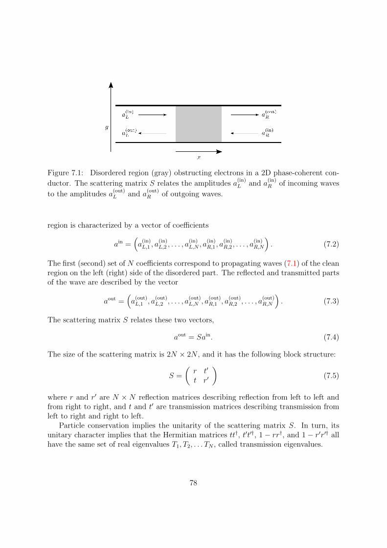
Figure 7.1: Disordered region (gray) obstructing electrons in a 2D phase-coherent con-
ductor. The scattering matrix S relates the amplitudes a(in)L and a
(in)R of incoming waves
to the amplitudes a(out)L and a
(out)R of outgoing waves.
region is characterized by a vector of coefficients
ain =(a
(in)L,1 , a
(in)L,2 , . . . , a
(in)L,N , a
(in)R,1 , a
(in)R,2 , . . . , a
(in)R,N
). (7.2)
The first (second) set of N coefficients correspond to propagating waves (7.1) of the cleanregion on the left (right) side of the disordered part. The reflected and transmitted partsof the wave are described by the vector
aout =(a
(out)L,1 , a
(out)L,2 , . . . , a
(out)L,N , a
(out)R,1 , a
(out)R,2 , . . . , a
(out)R,N
). (7.3)
The scattering matrix S relates these two vectors,
aout = Sain. (7.4)
The size of the scattering matrix is 2N × 2N , and it has the following block structure:
S =
(r t′
t r′
)(7.5)
where r and r′ are N × N reflection matrices describing reflection from left to left andfrom right to right, and t and t′ are transmission matrices describing transmission fromleft to right and right to left.
Particle conservation implies the unitarity of the scattering matrix S. In turn, itsunitary character implies that the Hermitian matrices tt†, t′t′†, 1− rr†, and 1− r′r′† allhave the same set of real eigenvalues T1, T2, . . . TN , called transmission eigenvalues.
78
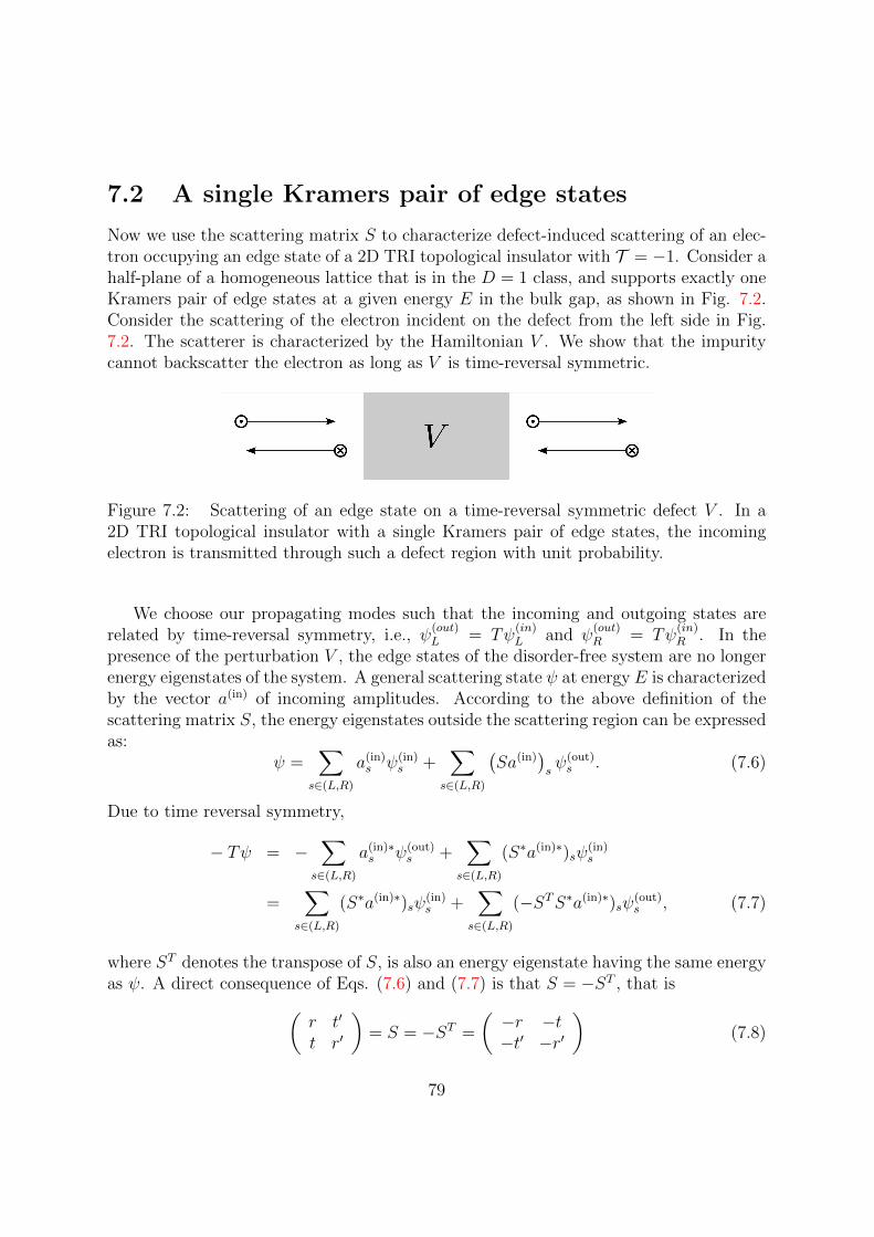
7.2 A single Kramers pair of edge states
Now we use the scattering matrix S to characterize defect-induced scattering of an elec-tron occupying an edge state of a 2D TRI topological insulator with T = −1. Consider ahalf-plane of a homogeneous lattice that is in the D = 1 class, and supports exactly oneKramers pair of edge states at a given energy E in the bulk gap, as shown in Fig. 7.2.Consider the scattering of the electron incident on the defect from the left side in Fig.7.2. The scatterer is characterized by the Hamiltonian V . We show that the impuritycannot backscatter the electron as long as V is time-reversal symmetric.
Figure 7.2: Scattering of an edge state on a time-reversal symmetric defect V . In a2D TRI topological insulator with a single Kramers pair of edge states, the incomingelectron is transmitted through such a defect region with unit probability.
We choose our propagating modes such that the incoming and outgoing states arerelated by time-reversal symmetry, i.e., ψ
(out)L = Tψ
(in)L and ψ
(out)R = Tψ
(in)R . In the
presence of the perturbation V , the edge states of the disorder-free system are no longerenergy eigenstates of the system. A general scattering state ψ at energy E is characterizedby the vector a(in) of incoming amplitudes. According to the above definition of thescattering matrix S, the energy eigenstates outside the scattering region can be expressedas:
ψ =∑
s∈(L,R)
a(in)s ψ(in)
s +∑
s∈(L,R)
(Sa(in)
)sψ(out)s . (7.6)
Due to time reversal symmetry,
− Tψ = −∑
s∈(L,R)
a(in)∗s ψ(out)
s +∑
s∈(L,R)
(S∗a(in)∗)sψ(in)s
=∑
s∈(L,R)
(S∗a(in)∗)sψ(in)s +
∑s∈(L,R)
(−STS∗a(in)∗)sψ(out)s , (7.7)
where ST denotes the transpose of S, is also an energy eigenstate having the same energyas ψ. A direct consequence of Eqs. (7.6) and (7.7) is that S = −ST , that is(
r t′
t r′
)= S = −ST =
(−r −t−t′ −r′
)(7.8)
79
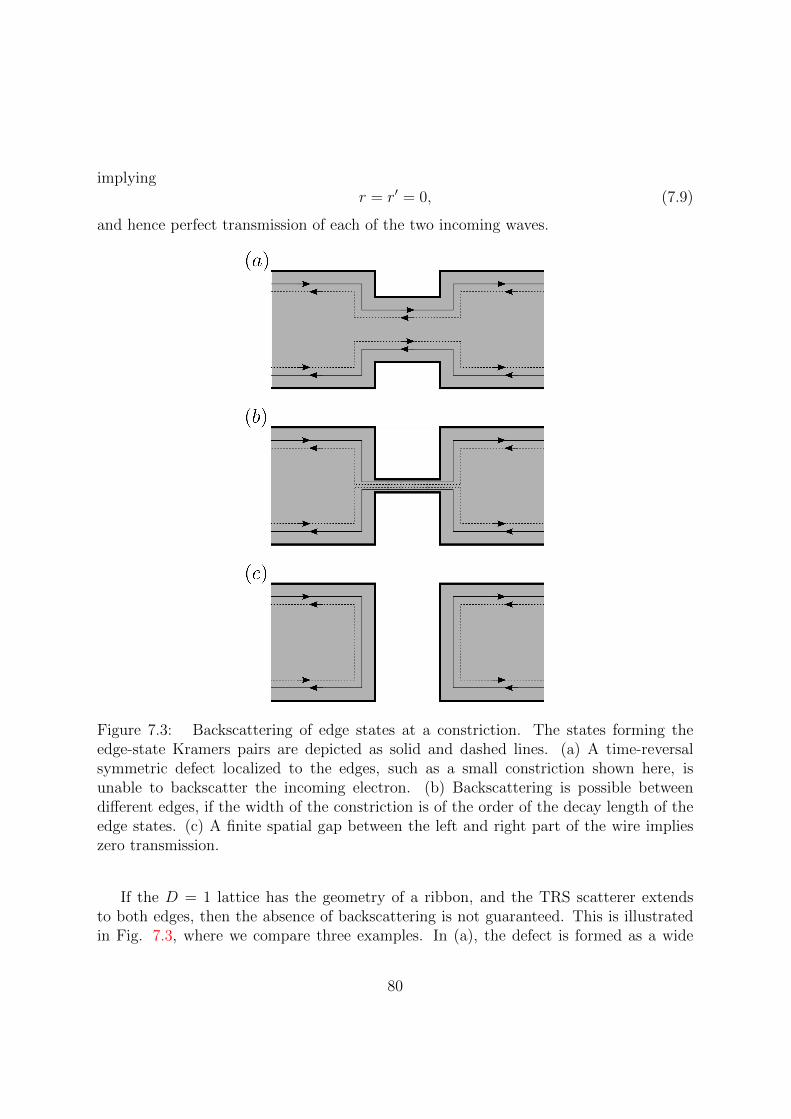
implyingr = r′ = 0, (7.9)
and hence perfect transmission of each of the two incoming waves.
Figure 7.3: Backscattering of edge states at a constriction. The states forming theedge-state Kramers pairs are depicted as solid and dashed lines. (a) A time-reversalsymmetric defect localized to the edges, such as a small constriction shown here, isunable to backscatter the incoming electron. (b) Backscattering is possible betweendifferent edges, if the width of the constriction is of the order of the decay length of theedge states. (c) A finite spatial gap between the left and right part of the wire implieszero transmission.
If the D = 1 lattice has the geometry of a ribbon, and the TRS scatterer extendsto both edges, then the absence of backscattering is not guaranteed. This is illustratedin Fig. 7.3, where we compare three examples. In (a), the defect is formed as a wide
80
constriction on both edges, with a width much larger than the characteristic length of thepenetration of the edge states to the bulk region of the ribbon. Backscattering betweenstates at the same edge is forbidden due to TRS, and backscattering between states atdifferent edges is forbidden due to a large spatial separation of their corresponding wavefunctions. In (b), a similar but narrower constriction with a width comparable to thepenetration length of the edge states does allow for scattering between states on thelower and upper edges. In this case, backscattering from a right-moving state on oneedge to a left-moving state at the other edge is not forbidden. In (c), the constrictiondivides the ribbon to two unconnected parts, resulting in zero transmission through theconstriction.
Naturally, backscattering is also allowed if the scatterer is not time-reversal sym-metric, or if the scattering process is inelastic. Backscattering is not forbidden for the‘unprotected’ edge states of topologically trivial (D = 0) 2D TRI insulators.
7.3 An odd number of Kramers pairs of edge states
The above statement (7.9) implying unit transmission, albeit in a somewhat weakenedform, can be generalized for arbitrary D = 1 lattice models, including those where thenumber of edge-state Kramers pairs N is odd but not necessarily one. The propositionis that in such a system, given a time-reversal symmetric scatterer V and an arbitraryenergy E in the bulk gap, there exists at least one linear combination of the incomingstates of energy E from each side of the defect that is perfectly transmitted through thedefect.
The proof follows that in the preceding Section, with the difference that the quantitiesr and t describing reflection and transmission are N × N matrices, and that the anti-symmetric nature of the S-matrix S = −ST implies the antisymmetry of the reflectionmatrices r = −rT . Every antisymmetric matrix has a vanishing determinant, thereforedet(r) = 0 and hence det(r†r) = det(r†) det(r) = 0, therefore at least one eigenvalue ofr†r is zero, which implies that at least one transmission eigenvalue Tn is unity.
7.4 Robustness against disorder
The absence-of-backscattering result (7.9) implies a remarkable statement regarding theexistence of (at least) one perfectly transmitting ‘edge state’ in a finite-size disorderedsample of a 2D TRI topological (D = 1) insulator. (See also the discussion about Fig. 4.8in the context of Chern Insulators). Such a sample with an arbitrarily chosen geometryis shown in Fig. 7.4. Assume that the disorder is TRS and localized to the edge of thesample. We claim that any chosen segment of the edge of this disordered sample supports,at any energy that is deep inside the bulk gap, (at least) one counterpropagating Kramers
81
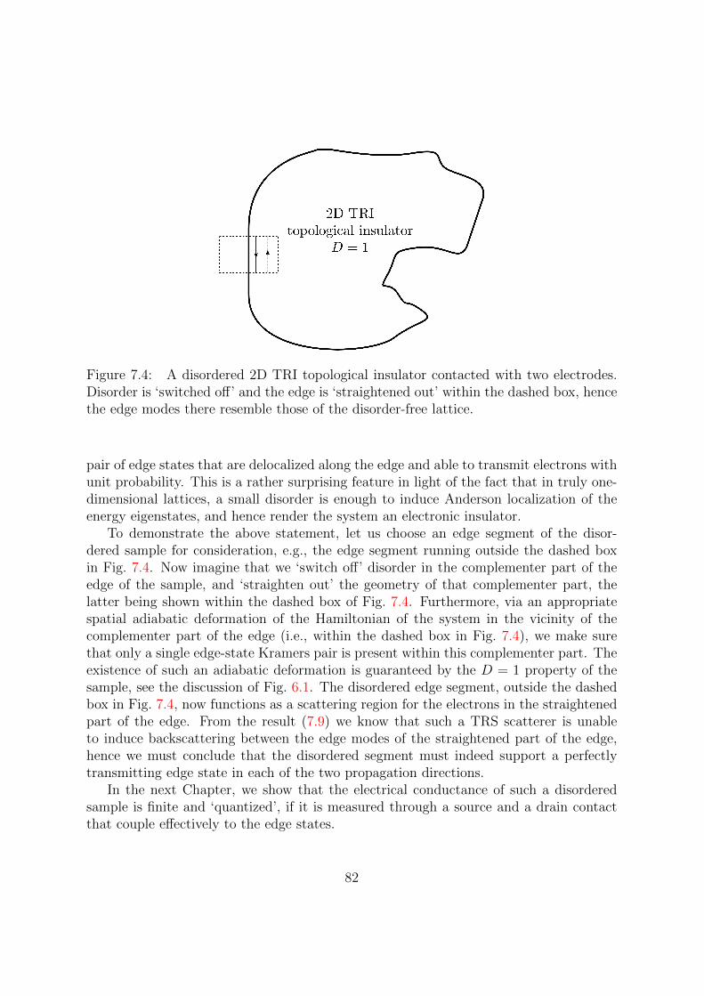
Figure 7.4: A disordered 2D TRI topological insulator contacted with two electrodes.Disorder is ‘switched off’ and the edge is ‘straightened out’ within the dashed box, hencethe edge modes there resemble those of the disorder-free lattice.
pair of edge states that are delocalized along the edge and able to transmit electrons withunit probability. This is a rather surprising feature in light of the fact that in truly one-dimensional lattices, a small disorder is enough to induce Anderson localization of theenergy eigenstates, and hence render the system an electronic insulator.
To demonstrate the above statement, let us choose an edge segment of the disor-dered sample for consideration, e.g., the edge segment running outside the dashed boxin Fig. 7.4. Now imagine that we ‘switch off’ disorder in the complementer part of theedge of the sample, and ‘straighten out’ the geometry of that complementer part, thelatter being shown within the dashed box of Fig. 7.4. Furthermore, via an appropriatespatial adiabatic deformation of the Hamiltonian of the system in the vicinity of thecomplementer part of the edge (i.e., within the dashed box in Fig. 7.4), we make surethat only a single edge-state Kramers pair is present within this complementer part. Theexistence of such an adiabatic deformation is guaranteed by the D = 1 property of thesample, see the discussion of Fig. 6.1. The disordered edge segment, outside the dashedbox in Fig. 7.4, now functions as a scattering region for the electrons in the straightenedpart of the edge. From the result (7.9) we know that such a TRS scatterer is unableto induce backscattering between the edge modes of the straightened part of the edge,hence we must conclude that the disordered segment must indeed support a perfectlytransmitting edge state in each of the two propagation directions.
In the next Chapter, we show that the electrical conductance of such a disorderedsample is finite and ‘quantized’, if it is measured through a source and a drain contactthat couple effectively to the edge states.
82
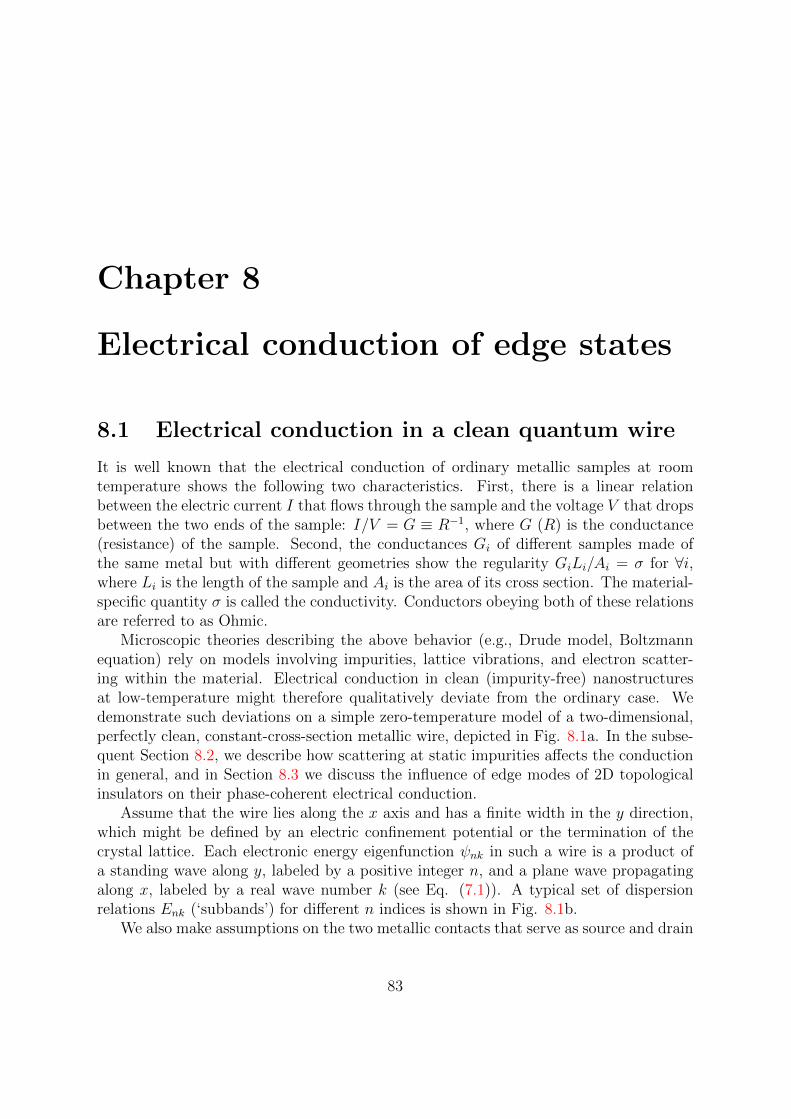
Chapter 8
Electrical conduction of edge states
8.1 Electrical conduction in a clean quantum wire
It is well known that the electrical conduction of ordinary metallic samples at roomtemperature shows the following two characteristics. First, there is a linear relationbetween the electric current I that flows through the sample and the voltage V that dropsbetween the two ends of the sample: I/V = G ≡ R−1, where G (R) is the conductance(resistance) of the sample. Second, the conductances Gi of different samples made ofthe same metal but with different geometries show the regularity GiLi/Ai = σ for ∀i,where Li is the length of the sample and Ai is the area of its cross section. The material-specific quantity σ is called the conductivity. Conductors obeying both of these relationsare referred to as Ohmic.
Microscopic theories describing the above behavior (e.g., Drude model, Boltzmannequation) rely on models involving impurities, lattice vibrations, and electron scatter-ing within the material. Electrical conduction in clean (impurity-free) nanostructuresat low-temperature might therefore qualitatively deviate from the ordinary case. Wedemonstrate such deviations on a simple zero-temperature model of a two-dimensional,perfectly clean, constant-cross-section metallic wire, depicted in Fig. 8.1a. In the subse-quent Section 8.2, we describe how scattering at static impurities affects the conductionin general, and in Section 8.3 we discuss the influence of edge modes of 2D topologicalinsulators on their phase-coherent electrical conduction.
Assume that the wire lies along the x axis and has a finite width in the y direction,which might be defined by an electric confinement potential or the termination of thecrystal lattice. Each electronic energy eigenfunction ψnk in such a wire is a product ofa standing wave along y, labeled by a positive integer n, and a plane wave propagatingalong x, labeled by a real wave number k (see Eq. (7.1)). A typical set of dispersionrelations Enk (‘subbands’) for different n indices is shown in Fig. 8.1b.
We also make assumptions on the two metallic contacts that serve as source and drain
83
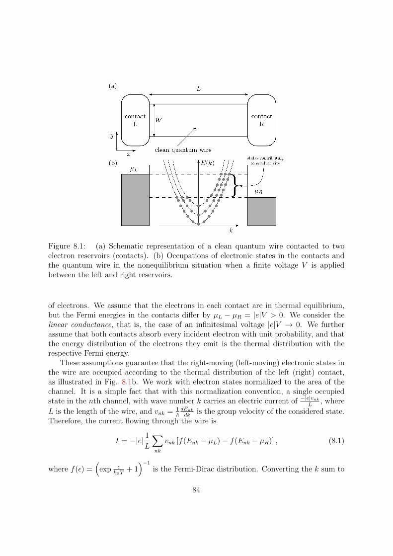
Figure 8.1: (a) Schematic representation of a clean quantum wire contacted to twoelectron reservoirs (contacts). (b) Occupations of electronic states in the contacts andthe quantum wire in the nonequilibrium situation when a finite voltage V is appliedbetween the left and right reservoirs.
of electrons. We assume that the electrons in each contact are in thermal equilibrium,but the Fermi energies in the contacts differ by µL − µR = |e|V > 0. We consider thelinear conductance, that is, the case of an infinitesimal voltage |e|V → 0. We furtherassume that both contacts absorb every incident electron with unit probability, and thatthe energy distribution of the electrons they emit is the thermal distribution with therespective Fermi energy.
These assumptions guarantee that the right-moving (left-moving) electronic states inthe wire are occupied according to the thermal distribution of the left (right) contact,as illustrated in Fig. 8.1b. We work with electron states normalized to the area of thechannel. It is a simple fact that with this normalization convention, a single occupiedstate in the nth channel, with wave number k carries an electric current of −|e|vnk
L, where
L is the length of the wire, and vnk = 1~dEnk
dkis the group velocity of the considered state.
Therefore, the current flowing through the wire is
I = −|e| 1L
∑nk
vnk [f(Enk − µL)− f(Enk − µR)] , (8.1)
where f(ε) =(
exp εkBT
+ 1)−1
is the Fermi-Dirac distribution. Converting the k sum to
84
an integral via 1L
∑k . . . 7→
∫dk2π. . . yields
I = −|e|∑n
∫dk
2π
1
~dEnkdk
[f(Enk − µL)− f(Enk − µR)] . (8.2)
The Fermi-Dirac distribution has a sharp edge at zero temperature, implying
I = −|e|hM
∫ µL
µR
dE = −|e|h
(µL − µR)M = Me2
hV (8.3)
Note that the first equality in (8.3) holds only if the number of subbands intersectedby µL and µR are the same, which is indeed the case if the voltage V is small enough.The number of these subbands, also called ‘open channels’, is denoted by the integerM . From (8.3) it follows that the conductance of the wire is an integer multiple of e2/h(commonly referred to as ‘quantized conductance’):
G =e2
hM. (8.4)
The numerical value of e2/h is approximately 40 µS (microsiemens), which correspondsto a resistance of approximately 26 kΩ. Note the the conductance quantum is definedas G0 = 2e2/h, i.e., as the conductance of a single open channel with twofold spindegeneracy.
It is instructive to compare the conduction in our clean quantum wire to the ordinaryOhmic conduction summarized above. According to (8.3), the proportionality betweenvoltage and current holds for a clean quantum wire as well as for an ordinary metal.However, the dependence of the conductance on the length of the sample differs qualita-tively in the two cases: in an ordinary metal, a twofold increase in the length of the wirehalves the conductance, whereas the conductance of a clean quantum wire is insensitiveto length variations.
Whether the conductance of the clean quantum wire is sensitive to variations of thewire width depends on the nature of the transversal modes. Conventional quantum wiresthat are created by a transverse confinement potential have a subband dispersion similarto that in Fig. 8.1b. There, the energy separation between the subbands decreases as thewidth of the wire is increased, therefore the number of subbands available for conductionincreases. This leads to an increased conductance for an increased width, similarly tothe case of ordinary metals. If, however, we consider a topological insulator, where thecurrent is carried by states localized to the edges of the wire, the conductance of the wirewill be insensitive to the width of the wire.
85
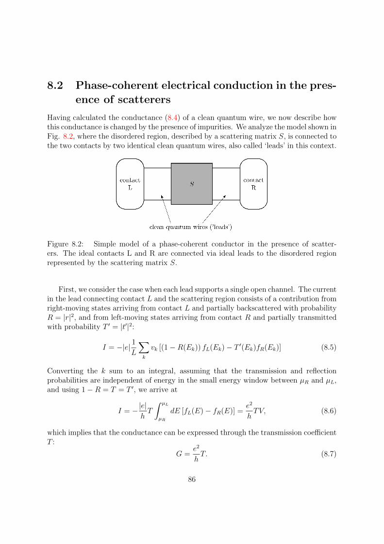
8.2 Phase-coherent electrical conduction in the pres-
ence of scatterers
Having calculated the conductance (8.4) of a clean quantum wire, we now describe howthis conductance is changed by the presence of impurities. We analyze the model shown inFig. 8.2, where the disordered region, described by a scattering matrix S, is connected tothe two contacts by two identical clean quantum wires, also called ‘leads’ in this context.
Figure 8.2: Simple model of a phase-coherent conductor in the presence of scatter-ers. The ideal contacts L and R are connected via ideal leads to the disordered regionrepresented by the scattering matrix S.
First, we consider the case when each lead supports a single open channel. The currentin the lead connecting contact L and the scattering region consists of a contribution fromright-moving states arriving from contact L and partially backscattered with probabilityR = |r|2, and from left-moving states arriving from contact R and partially transmittedwith probability T ′ = |t′|2:
I = −|e| 1L
∑k
vk [(1−R(Ek)) fL(Ek)− T ′(Ek)fR(Ek)] (8.5)
Converting the k sum to an integral, assuming that the transmission and reflectionprobabilities are independent of energy in the small energy window between µR and µL,and using 1−R = T = T ′, we arrive at
I = −|e|hT
∫ µL
µR
dE [fL(E)− fR(E)] =e2
hTV, (8.6)
which implies that the conductance can be expressed through the transmission coefficientT :
G =e2
hT. (8.7)
86
The result (8.7) can be straightforwardly generalized to the case when the leadssupport more than one open channel. The generalized result for the conductance, alsoknown as the Landauer formula, reads:
G =e2
h
M∑n=1
Tn, (8.8)
where Tn are the transmission eigenvalues of the scattering matrix i.e., the real eigenval-ues of the Hermitian matrix tt†, as defined in the preceding Chapter.
8.3 Electrical conduction in 2D topological insula-
tors
8.3.1 Chern Insulators
In Section 4.4, we have seen that an impurity-free straight strip of a topologically nontriv-ial Chern Insulator supports edge states. The relation between the Chern number Q ofthe Chern Insulator and the numbers of edge states at a single edge at a given energy E,propagating ‘clockwise’ (N+(E)) and ‘anticlockwise’ (N−(E)), is Q = N+(E)−N−(E).In addition, in Section 4.5 it was shown that any segment of the edge of a disorderedChern Insulator with Chern number Q and an arbitrary geometry supports |Q| chiraledge modes. Here we show that existence of these edge modes leads to experimentallydetectable effects in the electrical transport through Chern Insulator samples.
We consider a transport setup where the Chern Insulator is contacted with two metal-lic electrodes, as shown in Fig. 8.3. In this discussion, we rely on the usual assumptionsbehind the Landauer formula: phase-coherence of the electrons, good contact betweencontacts and sample, and large spatial separation of the two electrodes ensuring theabsence of tunneling contributions to the conductance.
In the following list, we summarize how the phase-coherent electrical conductance ofa Chern Insulator varies with the sample geometry, absence or presence of disorder, andthe value of the electronic Fermi energy.
1. Disorder-free sample with a strip geometry (see Fig. 8.1a)
(a) Fermi energy lies in a band. In this case, the sample is a clean quantum wire(see Section 8.1) with an integer number of open channels. The correspond-ing transversal wave functions might or might not be localized to the sampleedges, and therefore the number of channels might be different from any com-bination of Q, N+ or N−. According to Eq. 8.4, the conductance of such aclean quantum wire is quantized and insensitive to the length of the sample.Furthermore, the conductance grows in a step-like fashion if the width of thesample is increased.
87

Figure 8.3: A disordered sample of Chern insulator, with contacts 1 and 2, that can beused to pass current through the sample in order to detect edge states.
88

(b) Fermi energy lies in the gap. The sample is a clean quantum wire with openchannels that are all localized to the sample edges. The number of thosechannels is N+(E) +N−(E), where E is the Fermi energy: in each of the twopossible direction of current flow, there are N+ channels on one edge and N−on the other edge that contribute to conduction. Conductance is finite andquantized, a behavior rather unexpected from an insulator. The conductionis not Ohmic, as the conductance is insensitive to both the length and thewidth of the sample.
2. Disordered sample with an irregular shape (see Fig. 8.3):
(a) Fermi energy lies in a band. Because of the presence of disorder, the electricalconduction of such a sample is typically Ohmic. There are no protected edgestates at the Fermi energy.
(b) Fermi energy lies well within the gap. According to Section 4.5, any edgesegment of such a sample supports Q reflectionless chiral edge modes at theFermi energy. Therefore, conductance is typically quantized, G = |Q|e2/h,although, disorder permitting, it might in principle be larger than this value.The quantized conductance is insensitive to changes in the geometry or thedisorder configuration. This transport property, unexpected for an insulator,let alone for one with disorder, is a hallmark of Chern Insulators.
In the case of 2D samples there is often an experimental possibility of tuning the electronicFermi energy in situ by controlling the voltage applied between the sample and a nearbymetallic plate, as discussed in Section 8.4. This allows, in principle, to observe thechanges in the electrical conduction of the sample as the Fermi energy is tuned acrossthe gap.
8.3.2 2D TRI topological insulators with T 2 = −1
In the following list, we summarize the predictions of the Landauer formalism for theconductance of 2D TRI topological insulators with T 2 = −1 (‘D = 1 insulators’ forshort).
1. Disorder-free sample with a strip geometry:
(a) Fermi energy lies in a band. A simple consequence of the Landauer formula isthat phase-coherent conductance of an impurity-free D = 1 topological insu-lator of the strip geometry shown in Fig. 8.1a is quantized. The conductancegrows if the width of the strip is increased, but insensitive to change in thelength.
89
(b) Fermi energy lies in the gap. Only edge channels are open in this case. Thesealso provide conductance quantization. As the number of edge-state Kramerspair per edge is odd, the conductance might be 2e2/h, 6e2/h, 10e2/h, etc.Conductance is insensitive to width or length changes of the sample.
2. Disordered sample with an irregular shape and TRS disorder:
(a) Fermi energy lies in a band. The electrical conduction is Ohmic.
(b) Fermi energy lies in the gap. We have shown in Chapter 7 that a D = 1 insu-lator supports one protected edge-state Kramers pair per edge, which allowsfor reflectionless electronic transmission if only TRS defects are present. TheLandauer formula (8.8) implies, for typical cases, G = 2e2/h for such a sam-ple, as one edge state per edge contributes to conduction. The conductancemight also be larger, provided that the number of edge-state Kramers pairsis larger than 1 and disorder is ineffective in reducing the transmission of thetopologically unprotected pairs.
We note that in real materials with Z2 invariant D = 1, various mechanisms mightlead to backscattering and, in turn, to G < 2e2/h. Examples include TRS-breaking im-purities, TRS impurities that bridge the spatial distance between the edges (see Chapter7), hybridization of edge states from opposite edges in narrow samples, and inelasticscattering on phonons or spinful impurities.
8.4 An experiment with HgTe quantum wells
Electrical transport measurements [11] on appropriately designed layers of the semicon-ductor material mercury-telluride (HgTe) show signatures of edge-state conduction inthe absence of magnetic field. These measurements are in line with the theoretical pre-diction that a HgTe layer with a carefully chosen thickness can realize a topologicallynontrivial (D = 1) 2D TRI insulator with T 2nov = −1. In this Section, we outline themain findings of this experiment, as well as its relation to the BHZ model introducedand discussed in Chapter 6.
The experiments are performed on sandwich-like structures formed by a few-nanometerthick HgTe layer (quantum well) embedded between two similar layers of the alloyHgxCd1−xTe, as shown in Fig. 8.4. (In the experiment reported in [11], the alloy compo-sition x = 0.3 was used.) In this structure, the electronic states with energies close theFermi energy are confined to the HgTe layer that is parallel to the x-y plane in Fig. 8.4.The energy corresponding to the confinement direction z is quantized. The carriers arefree to move along the HgTe layer, i.e., parallel to the x-y plane, therefore 2D subbandsare formed in the HgTe quantum well. Detailed band-structure calculations of Ref. [3]show that as the the thickness d of the HgTe layer is decreased, the lowermost conduction
90
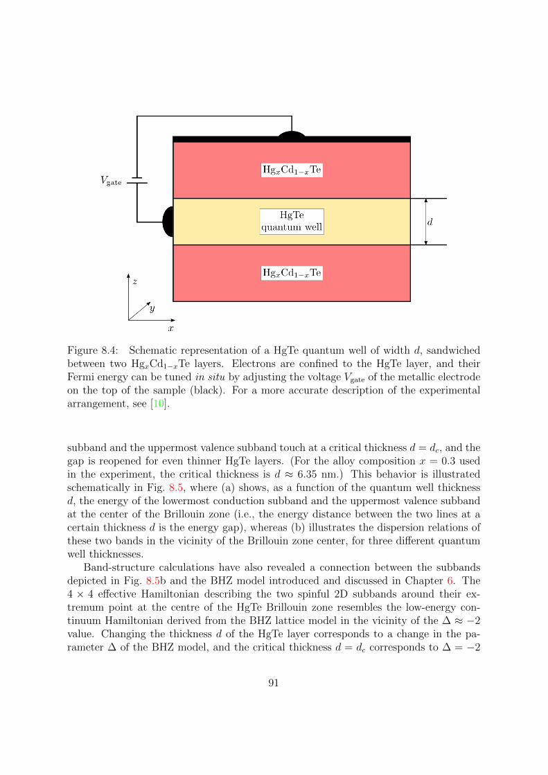
Figure 8.4: Schematic representation of a HgTe quantum well of width d, sandwichedbetween two HgxCd1−xTe layers. Electrons are confined to the HgTe layer, and theirFermi energy can be tuned in situ by adjusting the voltage Vgate of the metallic electrodeon the top of the sample (black). For a more accurate description of the experimentalarrangement, see [10].
subband and the uppermost valence subband touch at a critical thickness d = dc, and thegap is reopened for even thinner HgTe layers. (For the alloy composition x = 0.3 usedin the experiment, the critical thickness is d ≈ 6.35 nm.) This behavior is illustratedschematically in Fig. 8.5, where (a) shows, as a function of the quantum well thicknessd, the energy of the lowermost conduction subband and the uppermost valence subbandat the center of the Brillouin zone (i.e., the energy distance between the two lines at acertain thickness d is the energy gap), whereas (b) illustrates the dispersion relations ofthese two bands in the vicinity of the Brillouin zone center, for three different quantumwell thicknesses.
Band-structure calculations have also revealed a connection between the subbandsdepicted in Fig. 8.5b and the BHZ model introduced and discussed in Chapter 6. The4 × 4 effective Hamiltonian describing the two spinful 2D subbands around their ex-tremum point at the centre of the HgTe Brillouin zone resembles the low-energy con-tinuum Hamiltonian derived from the BHZ lattice model in the vicinity of the ∆ ≈ −2value. Changing the thickness d of the HgTe layer corresponds to a change in the pa-rameter ∆ of the BHZ model, and the critical thickness d = dc corresponds to ∆ = −2
91

Figure 8.5: Illustration of the evolution of the 2D band structure of a HgTe slab asa function of its thickness d. (a) Energies of the lowermost conduction subband andthe uppermost valence subband at the center of the 2D Brillouin zone, as a function ofquantum well thickness d. (b) Schematic dispersion relation of the two bands for a HgTequantum well for three different thicknesses.
and, consequently, a zero mass in the corresponding 2D Dirac equation.As a consequence of the strong analogy of the band structure of the HgTe quantum
well and that of the BHZ model, it is expected that either for d < dc or for d > dc thematerial is a D = 1 insulator with a single Kramers pair of edge states. Argumentspresented in [3] suggest that the thick quantum wells with d > dc are topologicallynontrivial.
Electrical transport measurements were carried out in HgTe quantum wells patternedin the Hall bar geometry shown in Fig. 8.6. The quantity that has been used in thisexperiment to reveal edge-state transport is the four-terminal resistance R14,23 = V23/I14,where V23 is the voltage between contacts 2 and 3, and I14 is the current flowing betweencontacts 1 and 4. This quantity R14,23 was measured for various devices with differentthicknesses d, below and above the critical thickness dc, of the HgTe layer, and fordifferent values of the Fermi energy. The latter can be tuned in situ by controlling the
92
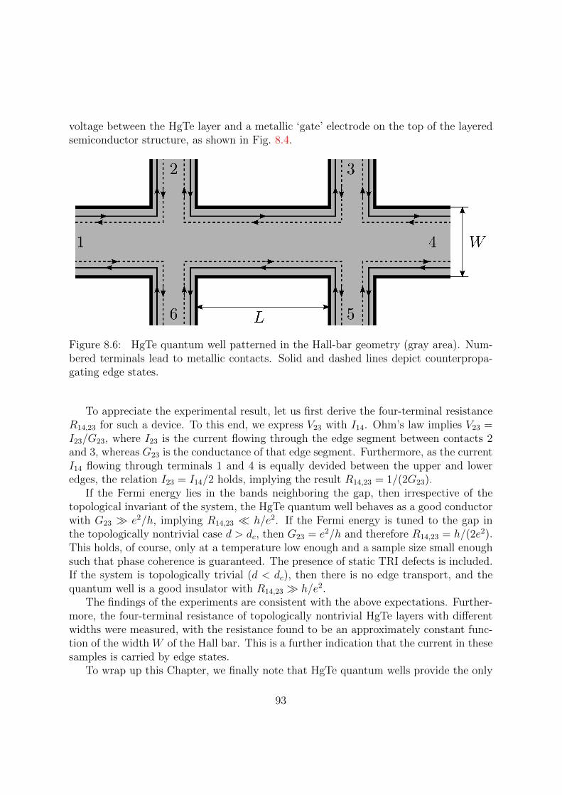
voltage between the HgTe layer and a metallic ‘gate’ electrode on the top of the layeredsemiconductor structure, as shown in Fig. 8.4.
Figure 8.6: HgTe quantum well patterned in the Hall-bar geometry (gray area). Num-bered terminals lead to metallic contacts. Solid and dashed lines depict counterpropa-gating edge states.
To appreciate the experimental result, let us first derive the four-terminal resistanceR14,23 for such a device. To this end, we express V23 with I14. Ohm’s law implies V23 =I23/G23, where I23 is the current flowing through the edge segment between contacts 2and 3, whereas G23 is the conductance of that edge segment. Furthermore, as the currentI14 flowing through terminals 1 and 4 is equally devided between the upper and loweredges, the relation I23 = I14/2 holds, implying the result R14,23 = 1/(2G23).
If the Fermi energy lies in the bands neighboring the gap, then irrespective of thetopological invariant of the system, the HgTe quantum well behaves as a good conductorwith G23 e2/h, implying R14,23 h/e2. If the Fermi energy is tuned to the gap inthe topologically nontrivial case d > dc, then G23 = e2/h and therefore R14,23 = h/(2e2).This holds, of course, only at a temperature low enough and a sample size small enoughsuch that phase coherence is guaranteed. The presence of static TRI defects is included.If the system is topologically trivial (d < dc), then there is no edge transport, and thequantum well is a good insulator with R14,23 h/e2.
The findings of the experiments are consistent with the above expectations. Further-more, the four-terminal resistance of topologically nontrivial HgTe layers with differentwidths were measured, with the resistance found to be an approximately constant func-tion of the width W of the Hall bar. This is a further indication that the current in thesesamples is carried by edge states.
To wrap up this Chapter, we finally note that HgTe quantum wells provide the only
93
experimental realization of D = 1 topological insulators to date. Graphene is believed tobe a D = 1 topological insulator as well, even though its energy gap between the valenceand conduction band, induced by spin-orbit interaction and estimated to be of the orderof µeV, seems to be too small to allow for the detection of edge-state transport even atthe lowest available temperatures. The concept of a TRI topological insulator can beextended to 3D crystals as well, where the role of the edge states is played by stateslocalized to the 2D surface of the 3D material. The description of such systems is out ofthe scope of the present course; the interested reader might consult, e.g., Refs. [7, 2].
94
Bibliography
[1] G. Bastard. Wave Mechanics Applied to Semiconductor Heterostructures. Les Edi-tions de Physique, Les Ulis, 1988.
[2] B. Andrei Bernevig. Topological Insulators and Topological Superconductors. Prince-ton University Press, 2013.
[3] B. Andrei Bernevig, Taylor L. Hughes, and Shou-Cheng Zhang. Quantum Spin HallEffect and Topological Phase Transition in HgTe Quantum Wells. Science, 314:1757,2006.
[4] M. V. Berry. Quantal phase factors accompanying adiabatic changes. Proc. R. Soc.Lond. A, 392:45–57, 1984.
[5] Takahiro Fukui, Yasuhiro Hatsugai, and Hiroshi Suzuki. Chern Numbers in Dis-cretized Brillouin Zone: Efficient Method of Computing (Spin) Hall Conductances.Journal of the Physical Society of Japan, 74(6):1674–1677, 2005.
[6] D.J. Griffiths. Introduction to Quantum Mechanics. Pearson Prentice Hall, 2005.
[7] M. Z. Hasan and C. L. Kane. Colloquium: Topological insulators. Rev. Mod. Phys.,82:3045, 2010.
[8] A. J. Heeger, S. Kivelson, J. R. Schrieffer, and W. P. Su. Solitons in conductingpolymers. Rev. Mod. Phys., 60:781, Jul 1988.
[9] Mahito Kohmoto. Topological Invariant and the Quantization of the Hall Conduc-tance. Annals of Physics, 160:343–354, 1985.
[10] Markus Konig, Hartmut Buhmann, Laurens W. Molenkamp, Taylor Hughes, Chao-Xing Liu, Xiao-Liang Qi, and Shou-Cheng Zhang. The Quantum Spin Hall Effect:Theory and Experiment. Journal of the Physical Society of Japan, 77(3):031007,2008.
95

[11] Markus Konig, Steffen Wiedmann, Christoph Brune, Andreas Roth, Hartmut Buh-mann, Laurens W. Molenkamp, Xiao-Liang Xi, and Shou-Cheng Zhang. QuantumSpin Hall Insulator State in HgTe Quantum Wells. Science, 318(6):766–770, 2007.
[12] Raffaele Resta. Berry Phase in Electronic Wavefunctions. Troisieme Cycle de laPhysique en Suisse Romande, 1996.
96