istanbul technical university graduate …“design of differential transimpedance amplifier in sige...
TRANSCRIPT

JANUARY 2014
ISTANBUL TECHNICAL UNIVERSITY GRADUATE SCHOOL OF SCIENCE
ENGINEERING AND TECHNOLOGY
DESIGN OF DIFFERENTIAL TRANSIMPEDANCE AMPLIFIER
IN SiGe BiCMOS FOR 10 Gbit/s FIBER OPTICAL RECEIVERS
M.Sc. THESIS
Yunus AKBEY
(504061235)
Department of Electronics and Communication Engineering
Electronics Engineering Programme
Anabilim Dalı : Herhangi Mühendislik, Bilim
Programı : Herhangi Program
Thesis Advisor: Prof. Dr. Osman PALAMUTÇUOĞULLARI


OCAK 2014
ĠSTANBUL TEKNĠK ÜNĠVERSĠTESĠ FEN BĠLĠMLERĠ ENSTĠTÜSÜ
10 Gbit/s FĠBER OPTĠK ALICILAR ĠÇĠN SiGe BiCMOS
FARKSAL GEÇĠġ-EMPEDANSI KUVVETLENDĠRĠCĠSĠ TASARIMI
YÜKSEK LĠSANS TEZĠ
Yunus AKBEY
(504061235)
Elektronik ve HaberleĢme Mühendisliği Anabilim dalı
Elektronik Mühendisliği Programı
Anabilim Dalı : Herhangi Mühendislik, Bilim
Programı : Herhangi Program
Tez DanıĢmanı: Prof. Dr. Osman PALAMUTÇUOĞULLARI


v
Thesis Advisor : Prof. Dr. Osman PALAMUTÇUOĞULRI …………...
İstanbul Technical University
Jury Members : Prof. Dr. Selçuk Paker ..................
İstanbul Technical University
Prof. Dr. Burak Polat ...................
Beykent University
Yunus Akbey, a M.Sc. student of ITU Graduate School of Science, Engineering
and Technology, student ID 504061235, successfully defended the thesis entitled
“Design of Differential Transimpedance Amplifier in SiGe BiCMOS For 10
Gbit/s Fiber Optical Receivers”, which he prepared after fulfilling the requirements
specified in the associated legislations, before the jury whose signatures are below.
Date of Submission : 12 December 2013
Date of Defense : 24 January 2014

vi

vii
To my mother and father,

viii

ix
FOREWORD
I would like to express my sincere appreciations to my supervisor Prof. Dr. Osman PALAMUTÇUOĞULLARI. Without his vision, encouragements and feedback, this dissertation would never become a reality.
My biggest gratitude goes to my mother and father for being with me and supporting me at every moment of my life. In this point, I want to open a page for my mother. She always supported me during my entire education life. She always tried to do her best to give me a big support during the preparation of this thesis.
My deepest gratitude goes to my sister and my brothers; Yeliz AKBEY, Ferit AKBEY and Emrah AKBEY. They have always been with me when I make an important decision/action in my life. They have generously given financial and spiritual supports whenever I need.
December 2013
Yunus AKBEY

x

xi
TABLE OF CONTENTS
Page
FOREWORD ........................................................................................................... ix TABLE OF CONTENTS .......................................................................................... xi ABBREVIATIONS ................................................................................................. xiii SYMBOLS .............................................................................................................. xv LIST OF TABLES ................................................................................................. xvii LIST OF FIGURES ................................................................................................ xix SUMMARY ............................................................................................................ xxi ÖZET ................................................................................................................... xxiii 1. INTRODUCTION .................................................................................................. 1 1.1 Purpose of the Thesis ..................................................................................... 2 1.2 Thesis Outline ................................................................................................. 3 2. FIBER OPTICAL COMMUNICATION SYSTEM ................................................... 5 2.1 Fiber Optic ...................................................................................................... 8 2.2 Photodiode.................................................................................................... 10 3. BACKROUND, THEORY AND DESIGN CONSIDERATIONS ........................... 13 3.1 Design Requirements ................................................................................... 14 3.1.1 Sensitivity and bit-error-rate .................................................................. 15 3.1.2 Bandwidth considerations and ISI ......................................................... 19 3.2 Transimpedance Amplifier Design ................................................................ 22 3.2.1 Transimpedance amplifier specifications ............................................... 23 3.2.1.1 Transimpedance ............................................................................ 23 3.2.1.2 Bandwidth and group delay ............................................................ 23 3.2.1.3 Noise .............................................................................................. 24 3.2.1.4 Wide input dynamic range .............................................................. 25 3.2.1.5 Output impedance .......................................................................... 26 3.2.2 TIA circuits concepts ............................................................................. 26 3.2.2.1 Open-loop TIA ................................................................................ 28 3.2.2.2 Feedback TIA ................................................................................. 29 3.2.2.3 Differential TIA ............................................................................... 35 3.3 Silicon-Germanium Heterojunction Transistors ............................................. 36 4. DESIGN OF DIFFERENTIAL TRANSIMPEDANCE AMPLIFIER in SiGe
BiCMOS FOR 10 Gbit/s FIBER OPTICAL RECEIVERS .................................... 39 4.1 Circuit Design ............................................................................................... 39 4.2 Simulation Results ........................................................................................ 46 5. CONCLUSION .................................................................................................... 53 REFERENCES ....................................................................................................... 55 APPENDICES ........................................................................................................ 59 CURRICULUM VITAE ............................................................................................ 65

xii

xiii
ABBREVIATIONS
ac : Alternating Current AGC : Automatic Gain Control AMS : Austria Micro Systems AlGaAs : Aluminum Gallium Arsenide BER : Bit-Error-Rate BiCMOS : Bipolar Complementary Metal Oxide Semiconductor BJT : Bipolar Junction Transistor BW : Bandwidth CD : Compact Disc CDR : Clock and Data Recovery CG : Common-Gate CMOS : Complementary Metal Oxide Semiconductor CMU : Clock Multiplication Unit dB : decibel dBm : decibelmili DC : Direct Current DMUX : Demultiplexer EMI : Electromagnetic Interference ELECO : Electrical and Electronics Engineering Conference erfc : Complementary Error Function FET : Field-Effect Transistor GaAs : Gallium Arsenide GaN : Gallium Nitride GB : Gigabyte Gb : Gigabit Gbit : Gigabit Ge : Germanium GSM : Global System for Mobile Communications HBT : Heterojunction Bipolar Transistor HEMT : High-Electron Mobility Transistor IC : Integrated Circuit InGaAs : Indium Gallium Arsenide InP : Indium Phosphate ISI : Intersymbol Interference ISSCC : International Solid-State Circuits Conference LA : Limiting Amplifier LAN : Local Area Network LD : Laser Diode MESFET : Metal-Semiconductor Field-Effect Transistor MOS : Metal Oxide Semiconductor MUX : Multiplexer NRZ : Non-Return-to-Zero PA : Post Amplifier PD : Photodiode PIN : p-intrinsic-n prbs : Pseudorandom Bit Sequence

xiv
P.M. : Phase Margin PO : Percent Overshoot pp : peak-to-peak rms : root mean square RF : Radio Frequency RZ : Return-to-Zero SDH : Synchronous Digital Hierarchy Si : Silicon SiO2 : Silicon Dioxide SNR : Signal to Noise Ratio SONET : Synchronous Optical Network TIA : Transimpedance Amplifier USA : United States of America VA : Voltage Amplifier WDM : Wavelength-Division Multiplexing

xv
SYMBOLS
A : voltage gain A0 : DC voltage gain BR : bit rate c : speed of light in vacuum Ccs : collector-substrate capacitance Cin : input capacitance Cnext : input capacitance of the next stage Co : total output capacitance Cout : output capacitance CP : photodiode junction capacitance CT : total input capacitance
C𝜇 : collector-base junction capacitance Cπ : collector-emitter capacitance f-3dB : bandwidth of TIA fT : unity-current gain frequency gm : transconductance h : Planck’s constant IB : base current IC : collector current iin : small-signal input current 𝒊𝒊𝒏,𝒑𝒑 : peak-to-peak input current
IPD : photodiode current
𝒊𝒔𝒆𝒏𝒑𝒑
: electrical sensitivity
𝒊𝒊𝒏 : averaged input current
𝒊𝒏,𝒊𝒏𝟐 : input-referred current spectrum
𝒊𝒏,𝒊𝒏,𝒕𝒐𝒕 : total input-referred noise current
𝒊𝒏,𝒊𝒏,𝒂𝒗𝒈 : averaged input-referred noise current
k : Boltzmann constant km : kilometer mm : millimeter nm : nanometer n+ : n-doped Q(x) : Q function q : electrical charge P : error probability
𝑷 : averaged optical power
𝑷𝒔𝒆𝒏 : optical sensitivity p+ : p-doped rb : base resistance RC : load resistor RF : feedback resistor Rout : output resistance RT : DC transimpedance gain s : second T : temperature in Kelvin Tb : bit period

xvi
t : time
𝒗𝒏,𝒕𝒐𝒕 : total integrated output noise
vo : small-signal output voltage vout : small-signal output voltage vpp : peak-to-peak value of the output signal
𝒗𝒏,𝒐𝟐 : output noise voltage spectrum
VTH : threshold voltage of the decision circuit |ZTIA(f)| : frequency-dependent transimpedance magnitude
𝒁𝑻 : transimpedance gain ζ : dimensionless damping ratio of a second-order system η : quantum efficiency of a photodiode θ(f) : frequency-dependent phase shift λ : wavelength of light μ : mobility ∆f : unity-frequency
∆𝝉 : group delay variation μm : micrometer
App : peak-to-peak microampere ℜ : responsivity of a photodiode τ : time constant
𝝉 𝝎 : group delay ωn : natural pulsation of a second-order system ω-3dB : bandwidth of a system Ω : ohm β : current gain

xvii
LIST OF TABLES
Page
Table 2.1 : SONET/SDH hierarchy ........................................................................... 6 Table 2.2 : PIN Photodiode operating wavelengths. ............................................... 11 Table 3.1 : BER and Q relationship. ....................................................................... 18 Table 4.1 : Device values and transistor emitter sizes. ........................................... 45 Table 4.2 : Transistor biasing points ....................................................................... 45 Table 5.1 : TIA performance summary and comparison some existing works ........ 54

xviii

xix
LIST OF FIGURES
Page
Figure 1.1 : Illustration of fiber optic receiver. ........................................................... 2 Figure 1.2 : Transimpedance amplifier design ......................................................... 3 Figure 2.1 : Fiber Optical Communication system .................................................... 6 Figure 2.2 : NRZ and RZ data modulation................................................................ 8 Figure 2.3 : Cross-section of fiber and fiber types .................................................... 8 Figure 2.4 : PIN Photodiode and approximate small-signal model ......................... 10 Figure 3.1 : A typical fiber optical front-end with shunt-feedback TIA. .................... 14 Figure 3.2 : Relationship between signal, noise and bit-error rate. ......................... 15 Figure 3.3 : Bit error probability at the CDR. .......................................................... 16 Figure 3.4 : Practical BER curve of a receiver. ....................................................... 18 Figure 3.5 : RC network for analyzing ISI (a) periodic square wave (b) random data .................................................................................. 20 Figure 3.6 : Bit rate versus bandwidth .................................................................... 21 Figure 3.7 : Typical shunt-feedback TIA. ................................................................ 22 Figure 3.8 : Low and high impedance TIA. ............................................................. 27 Figure 3.9 : Typical open-loop TIA topology. .......................................................... 28 Figure 3.10 : Second-order feedback transimpedance amplifier with small-signal
equivalent. ........................................................................................ 30 Figure 3.11 : Noise contributions in feedback TIA. ................................................. 33 Figure 3.12 : Photodiode capacitance, CP, effect on noise performance of TIA ...... 35 Figure 3.13 : Differential TIA with replicated capacitance. ...................................... 36 Figure 3.14 : Cross-section of vertical NPN SiGe transistor. .................................. 37 Figure 4.1 : Result of low bandwidth on Bessel and Butterworth TIAs. ................... 40 Figure 4.2 : Realized differential SiGe TIA schematic. ........................................... 42 Figure 4.3 : Half-circuit model of the differential SiGe TIA with photodiode small-
signal model. ....................................................................................... 43 Figure 4.4 : Differential transimpedance gain of the TIA ......................................... 46 Figure 4.5 : Group delay variation of the frequency response over the bandwidth . 47 Figure 4.6 : Total input-referred noise current spectrum of the differential TIA ....... 47 Figure 4.7 (a) : Differential output waveform of the circuit. The input data stream is
NRZ 10 Gbit/s 231 -1 PRBS. Input current is 15 App. ..................... 49 Figure 4.7 (b) : Differential output waveform of the proposed TIA. The input data
stream is NRZ 10 Gbit/s 231 -1 PRBS. Input current is 400 App .... 49
Figure 4.8 : Single-ended S22 parameter of the realized TIA. 30 resistors are
added to the both output for 50 matching ........................................ 50 Figure 4.9 (a) : Eye diagrams showing differential output at 10 Gbit/s 231 - 1 PRBS
data stream. Input current is 15 App, both outputs are loaded with 100 fF capacitor. ............................................................................ 51
Figure 4.9 (b) : Eye diagrams showing differential output at 10 Gbit/s 231 - 1 PRBS
data stream. Input current is 300 App, both outputs are loaded with 100 fF capacitor. ........................................................................... 51

xx
Figure 4.9 (c) : Eye diagrams showing differential output at 10 Gbit/s 231 - 1 PRBS
data stream. Input current is 15 App, both outputs are loaded with
50 resistors. 30 matching resistors are added to the both outputs. ........................................................................................ 52
Figure 4.9 (d) : Eye diagrams showing differential output at 10 Gbit/s 231 - 1 PRBS
data stream. Input current is 300 App, both outputs are loaded with
50 resistors. 30 matching resistors are added to the both outputs. ......................................................................................... 52
Figure A.1 : Program schematic of realized TIA .................................................... 61 Figure A.2 : Simulation and values ........................................................................ 62 Figure A.3 : Noise contribution of each device ...................................................... 63

xxi
DESIGN OF DIFFERENTIAL TRANSIMPEDANCE AMPLIFIER IN SiGe BiCMOS FOR 10 Gbit/s FIBER OPTICAL RECEIVERS
SUMMARY
After the beginning of 70s that first low loss silica fiber was presented, fiber optic communication has dominated to the telecommunication field and data transportation including short-haul and long-haul networks. The main reason for that fiber optic communication offers relatively very large bandwidth. Furthermore, the transmission using light keeps superior advantages over the conventional electrical communications such as no cross-talk, immune to the EMI, easy implementation and endurance.
Because fiber theoretically has enormous bandwidth and huge data transport capacity, heterostructure and heterojunction transistors such as GaAs and InP have dominated to photoreceivers since they exhibit very good bandwidth and noise performance simultaneously. SiGe BiCMOS however has provided cost-effective alternative for the realization of photoreceivers because SiGe BiCMOS can combine entire receiver in a single die. While high-gain, low-noise and high speed capability of SiGe is assisted for the analog part, CMOS circuits can build digital architecture of the optical receiver.
As for the receiver, the light transmitted by laser diode travels through fiber and experiences loss and dispersion before reaching a photodiode at the far end. The photodiode then senses the power of light and transforms the light intensity to a proportional photocurrent. At the receiver front-end, transimpedance amplifier (TIA) is an interface that converts the receiving photocurrent to electrical voltage. This amplified voltage generally is not enough for further digital processing. A second amplifier, namely post amplifier (PA), further increases the signal level. Clock and data recovery (CDR) extracts the digital data and clock information from the received signal. This is done by defining the threshold voltage. The pulse is assigned to “1” when the pulse amplitude is above the threshold voltage. In other case, when the pulse amplitude is lower than threshold voltage, the pulse is assigned to “0”. During recovery of the received data, CDR decides at the midpoint of each pulse in order to lower bit-error-rate (BER).
In addition to low power and single supply operation, TIA must exhibit linear phase response in order to be used for 10 Gbit/s applications. Trade-off between noise, speed, gain and supply voltage presents many challenges in TIA design. Overall sensitivity of the receiver is mostly determined by TIA because TIA is the first electrical part after photodiode. That being the case, TIA must maintain a reasonable signal gain as well as producing little noise to improve the sensitivity. It is also desirable to accommodate wideband data extending from almost dc to high frequencies to avoid intersymbol interference (ISI), which lowers BER. As performance indicators, BER is used to determine the bandwidth and the sensitivity, and the eye diagrams can be visual aids to estimate or to troubleshoot sources of noise and the other limiting factors. To meet these requirements, this study presents a new topology and compares it with the other transimpedance amplifier topologies.

xxii
In this thesis, the differential SiGe transimpedance amplifier for 10 Gbit/s fiber optical receivers is realized and its results are presented. The TIA is optimized for the best phase linearity over the bandwidth resulted in a group delay variation less than 1 ps. No inductor is used to achieve wideband operation. SiGe HBT BiCMOS enables TIA to be a cost-effective alternative and to integrate with other blocks of the fiber optical receiver. The differential structure of the TIA makes it immune to the effect of the supply and substrate noise. While flat frequency response with 9 GHz
bandwidth is obtained, differential transimpedance gain is almost 58 dB. The
electrical sensitivity of the proposed TIA is 15 App. Power consumption is 71 mW and maximum differential output swing is 320 mVpp. It is shown that the differential TIA is well suited for 10 Gbit/s data rate and OC-192 specifications.

xxiii
10 Gbit/s FİBER OPTİK ALICILAR İÇİN SiGe BiCMOS FARKSAL GEÇİŞ-EMPEDANSI KUVVETLENDİRİCİSİ TASARIMI
ÖZET
1970’lerin baĢında silika fiberin kaybının 20 dB/km düzeyinin altına indirilmesi sonucunda, telekomünikasyon sektöründe ve daha sonra internet ve veri paylaĢımı alanında fiber optiğin payı yıllar ilerledikçe artmıĢtır. ġüphesiz bunda etkili olan en büyük nedenler; ıĢığın kullanılmasıyla gerçekleĢtirilen veri transferinin EMI’den çok az etkilenmesi, çapraz-geçiĢin (cross-talk) çok az oluĢu, düĢük üretim ve montaj maliyetleri ve de dayanıklılık gibi fiber kablonun sağladığı üstünlüklerdir. Fiber optiğin en azından teorik olarak hali hazırda çok büyük bant geniĢliği sağlayabilmesi ve büyük veri taĢıma sığası sunması, daha hızlı uç elemanlarına ve elektronik tümdevrelerine gereksinim olduğu gerçeğini de beraberinde getirmiĢtir.
Yarıiletken teknolojisindeki yeni geliĢmeler sonucu ortaya çıkmıĢ bulunan heterostructure” ve “heterojunction” yarı iletken devre/kırmık elemanları, fiber iletiĢimin öngördüğü hızlı veri taĢıma ve düĢük gürültü özelliğini bir arada sunabildiklerinden, fiber optik alıcı ve vericilerinin uç elemanları olarak geniĢ kullanım alanı buldular.
SiGe çift kutuplu (bipolar) tranzistorunun geliĢtirilmesiyle, bu teknoloji ürünü tranzistorlar, fiber optik alıcılarında uç elemanı olarak kullanımlarında önem kazanmıĢlardır. SiGe teknolojisi, çift kutuplu Si tranzistorun Baz bölgesine belirli oranda Germanyum katkılanmasıyla, aynı boyutlardaki bilinen çift kutuplu tranzistora (BJT) göre daha büyük fT kesim sıklığı olanağını sunmuĢtur. Baz bölgesi dağılmıĢ direncinin de daha düĢük değerlere düĢmesi sonucunda da, daha düĢük gürültülü uç elemanlar gerçeklenebilmesine olanak sağlamıĢtır. Bu üstünlükleriyle SiGe, yukarıda sözü edilen III-V ve HBT yapılarıyla rekabet etme Ģansı bulmuĢtur. Ardından SiGe BiCMOS teknolojisi, alcının analog ve sayısal tüm öbeklerinin aynı kırmık üzerinde tümleĢtirme olanağını da sunabildiğinden, düĢük gürültülü, geniĢ bantlı ve düĢük maliyetli çözümler gerçeklemede söz konusu alanlar için çok çekici olmuĢlardır.
Vericideki lazer diyot aracılığı ile sayısal veri, ıĢık kaynağına dönüĢtürülür ve fiber kabloya gelir. Fiber kablo içinde yitime ve dağılıma (dispersion) uğratılan, modüle edilmiĢ (kodlanmıĢ), sayısal bilgi taĢıyıcısı ıĢık, alıcıdaki foto diyot tarafından yeniden elektrik akımına dönüĢtürülür. Burada bu elektrik akımı, önce TIA tarafından yükseltilip kendisiyle orantılı gerilime dönüĢtürüldükten sonra, ikincil kuvvetlendirici ile (post amplifier, PA) genliği daha da artırılarak saat devresine (clock and data recovery, CDR) gönderilir. Saat devresinde saat iĢareti ve veri bilgisi ayrıĢtırılır ve daha küçük hızlara azaltılmak için “DEMUX” devresine gönderilir. CDR bir eĢik gerilimi üretir. Bu eĢik geriliminin üzerindeki genlik sayısal “1”, altındaki genlik sayısal “0” olarak belirlenir. Burada CDR, bu süreci gerçekleĢtirmek için her bir darbe süresinin tam ortasında karar verir. Bunu yapmasının nedeni dağılıma ve bozunuma uğratılmıĢ iĢaretteki farklılaĢmaları göz önüne alarak en güvenli bit çözümlemesini gerçekleĢtirmesidir.
Bu noktada TIA tasarımının büyük önemi bulunmaktadır. Çünkü TIA iĢaretin foto diyottan sonra uğradığı en ön kattır ve bütün alıcının gürültüsünü büyük oranda bu katın gürültüsü belirleyecektir. Dolayısıyla gerçekleĢtirilecek TIA’nın düĢük gürültülü

xxiv
olması gereklidir. Dağılım/bozunum etkilerinden kaynaklanan kare dalgadaki bozulmalar, gürültünün de etkisiyle her bir darbenin CDR tarafından yanlıĢ çözümlenme olasılığını artıracaktır. Bunun önüne geçmek için alıcının duyarlılığı belirli bir hata payı üzerinden hesaplanır. Doğal olarak, TIA’nın bu duyarlılığa etkisi büyüktür. Bu duyarlılık, fiber iletiĢim kurallarının belirlediği bit-hata-oranı (bit-error-rate, BER) üzerinden hesaplanır ve göz diyagramları (eye diagrams) çıkıĢtaki iĢaretin ne derece düzgün olduğunu görmemizi sağlar.
Bu projede 10 Gbit/s gibi hızlı bir uygulama hedeflendiğinden TIA’nın geniĢ bantlı olması gerekeceği açıktır. Bu düzeydeki bir hızla modüle edilmiĢ iĢaret; bant geniĢliği yeterli olmayan bir TIA’ya uğradığında, iĢarette bozulmalar meydana gelecek ve göz diyagramında yatay ve dikey kapanmalar gözlenecektir. Bununla birlikte gereğinden fazla bant geniĢliği giriĢte daha büyük toplam gürültüye neden olacağından, TIA’nın bant geniĢliği ve gürültüsü arasında bir uzlaĢının sağlanması gerektiği açıktır. 10 Gbit/s NRZ koduna sahip veri iĢareti için yaklaĢık 7 GHz bant geniĢliğine sahip bir uç devresi fiber optik alıcılar için yeterli olabilmektedir.
Sıklık (frekans) domenindeki düzgün sıklık tepesi ve yeterli bant geniĢliği ölçümleri, çıkıĢtaki iĢaretin Ģeklinin düzgün olabilmesi için yeterli değildir. Dolayısıyla iĢaretin evresindeki (phase) değiĢimler de gözlemlenmelidir. Yeteri kadar doğrusal olmayan evre tepkesi ya da düĢük evre paylı iĢaret, geçici rejim (transient) ölçümlerinde aĢımlara neden olabilmektedir.
Gürültü ve hız arasındaki optimizasyonda TIA’nın kazancı, düĢük güçlü ve tek besleme kaynağına sahip olması gibi diğer önemli ve ayırt edici özelliklerin de eklenmesiyle, TIA tasarımında bu özelliklerin arasından istenen hız için en optimum performansı sağlayacak sonuçlar elde edilmeye çalıĢılmalıdır. Çünkü sahip olunan yarı iletken teknolojisinin özellikleri ulaĢılabilecek performansı büyük ölçüde belirlemektedir.
Büyük geçiĢ-empedansı (transimpedance) kazancı elde etmek aynı zamanda büyük bant geniĢliği elde etmeyi sınırladığından genellikle ikincil kuvvetlendiriciye ihtiyaç duyulur. Bu ikincil kuvvetlendiriciler farksal yapıya sahiptir. CDR’deki veri çözümleme iĢlemi için birkaç yüz mili volt yeterli olabilmektedir. Dolayısıyla TIA’dan elde edilecek 50-60 dBΩ mertebelerindeki kazanca ilaveten 30-40 dB aralıklarında ikincil kuvvetlendiriciye ihtiyaç olacaktır.
TIA’nın fark kuvvetlendiricisi Ģeklinde tasarlanması güç kaynağı dalgalanmalarını, ortak biçim gürültüsünü ve parazitik etkenlerin neden olabileceği kararsızlık sorunlarını büyük ölçüde giderir. Aynı zamanda ikincil kuvvetlendiricide ayrıca bir referans gerilim üretecini gerekli kılmaz. Bu anlamda farksal yapıyı ihtiva eden TIA tekil yapıya göre daha avantajlıdır. Ancak farksal yapıdaki ilave tranzistorlar ve tümdevre elemanları, gürültünün artmasına dolayısıyla duyarlılığın kötüleĢmesine de neden olacaktır. Ġlaveten, foto diyotun tek çıkıĢ üretmesine karĢılık TIA’nın iki giriĢi olması, asimetrik sorunlara neden olacaktır. Bunun için bu çalıĢmada foto diyot TIAnın diğer ucunda da modellenmiĢtir.
TIA tasarımında yukarıda belirtilen performans ölçütlerine ulaĢmak için geliĢtirilen/sunulan değiĢik devre yapıları ve performans arttırıcı teknikler kaynaklarda vardır. Bu çalıĢmada bunlara değinilmiĢ ancak tasarlanan devrenin iyi sonuçlar vermesiyle bu yapıları kullanmaya gereksinim kalmamıĢtır.
Bu çalıĢmada 10 Gbit/s hızındaki fiber optik uygulamaları için fiber optik alıcının en önemli katlarından birisi olan geçiĢ-empedansı kuvvetlendiricisi (transimpedance amplifier) tasarlanmıĢ, devrenin benzetimleri gerçekleĢtirilmiĢ ve sonuçları sunulmuĢtur. Söz konusu yarı iletken teknolojisi ile en iyi devre yapıları ve mimarileri incelenmiĢ, analizleri ve benzetimleri yapılmıĢtır. En iyi sonuçlar paralel-direnç geri besleme devresi kullanılarak elde edilmiĢtir.

xxv
Düzgün bir sıklık tepesi ile 9 GHz kesim frekansı elde edilmiĢtir. Ġlaveten, oldukça doğrusal evre tepkesi sonucuna ulaĢarak, 1ps den daha az grup gecikmesi (group
delay) değiĢimi elde edilmiĢtir. 58 dBΩ farksal TIA kazancı sağlanmıĢ ve 1.061 μA toplam giriĢ gürültüsü ile 15 μApp elektrik duyarlılığı elde edilmiĢtir. En yüksek farksal çıkıĢ iĢareti salınımı 320 mVpp’dir. Güç tüketimi tek besleme kaynağından, 3.3 V ile 71 mW’dır. Her bir TIA tasarımı için ayırt edici ölçüt olan ortalama giriĢ gürültüsü
11.18 pA/ 𝐻𝑧’dir. Gerçeklenen TIA, PA ile aynı kırmık içinde gerçeklenmemesi durumunda, S22 benzetimi 1 GHz ile 9 GHz arasında -15 dB’in altında kalacak Ģekilde elde edilmiĢtir. Gerçeklenen devre 10-Gbit/s hızı için ve SONET OC-192 standartları için uygun bir devredir.

xxvi

1
1. INTRODUCTION
The growth of telecommunication and the surge in data communication mandates
the use of broadband communication systems. Fiber optical communication systems
have been an attractive solution to cope with the high-speed data rates and to
transport the huge amount of data capacity for both long-haul and short-haul
transmission systems. Together with the high-speed HBT and III-V technologies
(later deep submicron CMOS has taken place in this race), light transmission
through fiber has made an incredible progress in the telecommunication field and
internet.
Until recent years, high cost, high power III-V devices (GaAs MESFETs,
AlGaAs/GaAs HEMTs, AlGaAs/GaAs HBTs) have occupied fiber optical receivers
since they present very high bandwidth solutions. Recently, SiGe technology has
taken the place, which exhibits large fT as well as performing low power and low
noise behavior. With the employing of SiGe BiCMOS technology; low-cost, high-
performance integrated fiber optical receivers come into prominence.
An optical receiver converts the optical signal received at the output end of the
optical fiber back into the original electrical signal. The illustration of optical receiver
is given in Figure 1.1. As being the first building block after photodiode,
transimpedance amplifier (TIA) amplifies electrical current with sufficient bandwidth,
converting it to a voltage, while adding as little noise as possible. That being the
case, TIA is without a doubt the most critical building block of the optical receiver.
The design of this block involves many trade-offs between noise, bandwidth, gain
and stability. This dissertation tries to reveal all subtleties and challenges
encountered during the design of low-noise, high-bandwidth differential TIA.
The most common TIA configuration is the shunt-feedback TIA topology, where a
negative feedback network senses the voltage at the output and returns a
proportional current to the input. This type of feedback is chosen in this study
because it shows very good performance for the given technology and it is well
suited for intended speed.

2
Figure 1.1: Illustration of fiber optic receiver.
1.1 Purpose of the Thesis
The purpose of this thesis is to accomplish a transimpedance amplifier for the 10
Gbit/s fiber optical receivers. The goal is to provide output signal having wide
bandwidth and low-noise as well as sustaining suitable gain. Even if required cut-off
frequency for the 10 Gbit/s NRZ data rate is about 7 GHz, 8-9 GHz bandwidth is
intended. Since required signal amplitude for the data recovery is several hundreds
milivolts, transimpedance gain between 50-60 dB/Ω gain is aimed. The remaining
gain has to be carried out at the post amplifier because of tight noise and bandwidth
restrictions stemming from TIA design. Differential topology is another scope to
eliminate common-mode noise. Semiconductor technologies including CMOS will
make presented TIA easily to combine with subsequent stages of the receiver and
thus SiGe BiCMOS process is preferred for this work.

3
Figure 1.2: Transimpedance amplifier design.
1.2 Thesis Outline
This work presents a differential, broadband and low-noise transimpedance amplifier
for 10 Gbit/s fiber links using SiGe HBT BiCMOS process.
In Section 2, some important information about the fiber communication is given.
Fiber optic receiver components such as fiber optic cable and photodiode
specifications are also investigated.
Section 3 provides background and theoretical basics as well as resolving the
evolving design complexity. Receiver fundamentals such as BER are explained. The
most important TIA specifications are emphasized. Finally, TIA circuit types are
searched for the best circuit performance.
In section 4, design platform and technology process are discussed. Explanations
about the methodology to achieve projected performance are provided. The
proposed TIA is investigated and the design is achieved. After the realization of the
theoretical circuit, results are presented. Eventually, conclusions and further
explanations are covered in Section 5.

4

5
2. FIBER OPTICAL COMMUNICATION SYSTEM
The rapid rise of internet traffic and the need for high capacity data transmission for
local area networks have made optical communications the best choice for high
speed data transmission. Compared to the conventional electrical communications,
the communication using optical carrier waves is usually immune to electromagnetic
interference and cross talks, offers very high bandwidth usage, provides low
transmission losses at very high frequencies, includes good overall system reliability
and maintenance. Free space RF transmission is flexible and cheap, but it cannot
support large bandwidths and requires fairly large power to transmit over long
distances. Free space optical transmission is also quite flexible, but the signal
quality and propagation distance are weather-dependent. Standard RF signal
propagation over coaxial cable is simple to integrate with standard electronics and is
ideal for relatively short distances and low data rates [1]. Due to the advantages
stated above, fiber optical transmission system is widely realized in areas such as
long-haul transmissions, local area networks, inter-city telecommunication, cable TV
etc.
The Synchronous Optical Network (SONET) and Synchronous Digital Hierarchy
(SDH) standard govern the fiber optic transmission schemes. While SONET
regulates the requirements in the USA, SDH standards are for Japan and Europe
zone. These standards define the technology, performance and specifications
required by the fiber optical systems through a synchronous, flexible, optical
hierarchy by means of multiplexing scheme [2], which is shown in Table 2.1.
These transmission data rates and their standards have been issued over the years
as the need for high capacity traffic is increased. Since the intended speed of this
design is 10 Gbit/s, OC-192 hierarchy specifications are to be cared.

6
Table 2.1: SONET/SDH hierarchy.
SONET SDH Bit Rate
OC-1 - 51.84 Mbit/s
OC-3 STM-3 155.52 Mbit/s
OC-12 STM-4 622.08 Mbit/s
OC-48 STM-16 2.4883 Gbit/s
OC-192 STM-64 9.9533 Gbit/s
OC-768 STM-196 39.8131 Gbit/s
A figure to give a quick understanding about conversion of data between electrical
signal and light is shown in Figure 2.1. The modulation of the data to light takes
place at the optic transmitter. The laser driver converts the data, in the form of an
electrical signal, to current. Light is produced with the current responding the laser
diode. The data-modulated light is channeled to the receiver via a fiber guide. The
receiver uses a photodiode to convert the incoming light to current. The data is
recovered by two amplification stages: Transimpedance amplifier (TIA) and post
amplifier (PA). TIA, which is the main target of this thesis and will be largely
discussed in the next, converts the current to a low-noise voltage signal.
Figure 2.1: Fiber Optical Communication system.
Depending on whether the optical signal is transmitted over relatively long or short
distances, fiber communication transmission can be classified into two categories:
long-haul and short-haul communications. Long-haul communication systems (like
inter-continents) require high capacity, high bandwidth trunk lines. Periodic
regeneration and amplification of the optical signal by using repeaters (both

7
electronic and optical amplifiers) is still required for most long-haul systems. Short-
haul communication applications cover intercity and local-loop traffic. Such systems
operate at lower bit rates over distances of less than 50 km [2].
The data transport capacity of a single fiber is improved by applying Wavelength
Division Multiplexing scheme (WDM), which simultaneously transmits many data
streams on to the single fiber at different wavelengths. Although the WDM scheme
described above provides large data shipping ability, there are some technology
limitations in providing a number of wavelengths, such as channel broadening
effects, non-ideal optical filtering and the limited channel wavelength spacing for the
desired performance.
There are mainly two types of modulation format used in optical fiber
communication: Non-return-to-zero (NRZ) and return-to-zero (RZ). The NRZ is a
kind of on-off keying, meaning the signal is on to transmit the “one” bit and is off to
transmit the “zero”. In RZ, however, the data returns to “zero” after every bit to allow
safe propagation of pulses. As it is seen from the Figure 2.2, the duration of “one”
pulses (half of the pulse duration of NRZ) are less than that of NRZ. Therefore, RZ
format tolerate pulse spreading and intersymbol interference (ISI) due to the
dispersion, allowing better decision threshold. It is used in long-haul systems due to
the dispersion performance.
As it will be dealt with in the following chapter, NRZ signal enables front-end of the
receiver to have lower bandwidth (BW) for the same data rate (BR). The bandwidth
is 0.7BR in NRZ while it is approximately two times the bit rate in RZ modulation.
This specification makes the NRZ the most commonly used one at 10 Gbit/s
applications [3, 5]. During the whole design, NRZ modulation format is taken into
account.
Right before digital data is modulated on optical carrier, they are usually
preconditioned dictated by SONET specifications. The preconditioning, namely line
coding, provides transmitted bit stream to have the properties such as short run
lengths and high transition density. It is desirable to control the number of
successive zeros and ones for the small value. This approach limits the DC wander
effect allowing the use of AC coupling in receiver design. In SONET specifications,
generally, more than 72 consecutive bits are not allowed and this condition is
sustained using scrambling.

8
Figure 2.2 : NRZ and RZ data modulation.
2.1 Fiber Optic
Figure 2.3 depicts the cross-section of fiber structure. In its simplest form, an optical
fiber consists of a cylindrical core of silica glass surrounded by a cladding whose
refractive index is lower than that of the core. The outer jacket is called the cable,
which acts as waveguides for the optical signal. The cable can contain one or more
fibers.
Figure 2.3: Cross-section of fiber and fiber types [6].
The role of a communication channel is to transport the optical signal from the
transmitter to the receiver with as little loss and dispersion as possible. Like other
communication channels, fiber cable also attenuates the signal, which is called the
fiber loss due to the scattering, absorption by material impurities or other effects. In
60s, when the fiber was first presented, the loss was about 1000 dB/km. it was

9
during 70s that low loss fiber (less than 20 dB/km) started to be produced, which
made the fiber an important candidate for the broadband communications. Today,
silica fiber loss is around 0.18-0.2 dB/km [7].
The short history stated above is for the silica-based fiber. There is another type of
fiber having much amount of loss (55 dB/km) is the plastic fiber. The plastic optical
fiber bears the advantage of low cost, enduring and ease implementation such that
they are mostly preferred for very short applications.
Dispersion, which is actually a kind of distortion, is the broadening of individual
optical pulses during propagation through the fiber. If optical pulses spread
significantly outside their allocated bit slot, then the transmitted signal is severely
degraded. Eventually, it becomes impossible to recover the original signal with high
accuracy at the decision circuit. This unwanted phenomenon appears as ISI and
jitter on the eye diagrams.
The silica glass has two low loss operating wavelength windows. One is around
wavelength λ=1.3 μm and the other one is at λ=1.55 μm. At the 1.55 μm
wavelength, silica fiber has the lowest loss which is about 0.2 dB/km whereas it is
about 0.4 dB/km for the λ=1.3 μm medium. However, the dispersion is lowest at the
1.3 μm window [5]. The operating region of plastic fiber is 0.75-0.82 μm while
maintaining lowest dispersion in this window as well.
Fiber optic cable can also be classified according to the operating mode. When the
only one ray light propagates through the fiber at only one path, it is called single
mode fiber. As it is seen from the Figure 2.3, multimode fibers have relatively bigger
core allowing the light to take multiple pathways. That multimode operation
increases the data capacity of the channel. Dispersion issue is the most severe in
the case of multimode fibers since pulses spread rapidly because of different
speeds associated with different fiber modes. It is, for this reason, used for shorter
distances. Most optical communication systems use single-mode fibers because
single-mode fibers are better at retaining the originality (or shape) of each light pulse
over long distances than multimode fibers [2].

10
2.2 Photodiode
The first part of an optical receiver is the photodetector. The photodiode is a square
law device, which means that the detected electrical current depends on the power
of the incident optical signal. The main characteristics of this device are its
responsivity, speed and the leakage current. As it is given and plotted in section 3,
the receiver’s sensitivity is largely determined by the capacitance of the
photodetector together with the input impedance of the transimpedance amplifier.
Semiconductor photodiodes are used in fiber optical receivers as photodetectors
because of their compatibility with the whole system. Phototransistor is not preferred
in high-speed applications due to the high base-collector junction capacitance C𝜇.
PIN (p-i-n) photodiode is widely used in high-speed applications (2.5-40 Gbit/s).
Figure 2.4 illustrates structure and approximate small-signal model of a PIN
photodiode.
Figure 2.4: PIN Photodiode and approximate small-signal model.
In the intrinsic region or depletion region (undoped or lightly doped), the conversion
of the light to the electric current occurs by means of absorbing photons. Photons
incident on i-layer creates electron-hole pairs. Reverse biased p-doped p+ and n-
doped n+ regions creates strong electric field in the depletion material. Because of
this strong reverse polarization, separated electron and holes created by light are
absorbed to opposition polarities producing continuous current. Ideally, every photon
must create an electron-hole pairs. However, due to the reasons such as thermal

11
effects, absorption imperfections, this condition cannot be met. This is called
quantum efficiency, η [2].
Semiconductor photodiodes used in photoreceivers have operating wavelength at
which they absorb photos in accordance with their quantum efficiency. Table 2.2
gives operating wavelength of the most available photodiodes types. Because of the
operation principals of light in a medium, photodiode choice is not an easy choice for
the designer. For instance, for the high-speed silica glass fiber, InGaAs photodiode
is a popular choice because of its high performance [8].
Table 2.2: PIN Photodiode operating wavelengths.
Semiconductor Wavelength
Silicon 750-850 nm
Germanium 1100-1600 nm
GaAs 700-850 nm
InGaAs 1100-1700 nm
InGaAsP 1100-1600 nm
In the small-signal model of Figure 2.4, photodiode is modeled only with p-n junction
capacitance, Cp. This model is enough for the simulation and design performance
because the intrinsic resistance of contacts and bond wire is too small that it can be
ignored. Likewise, shunt junction resistance can be ignored because of the wide
intrinsic region [9]. As it will be stated in the following, the input impedance of the
TIA is the most important design criteria, which is mostly determined by Cp. To get
intuitive understandings about sensitivity given in the next section, it is helpful to
give figure-of-merit equation of PIN photodiode. It is [9]
𝐼𝑃𝐷 = ℛ.𝑃 (2.1)
Where 𝐼𝑃𝐷 is the photodiode current produced for a given amount of optical power
P. ℛ is the responsivity of PIN photodiode given by
ℛ = 𝜂𝜆𝑞
𝑐 (2.2)

12
Where q is the electric charge, h is the Planck constant; c is the speed of light in
vacuum. The responsivity of typical InGaAs PIN photodetector is typically in the
range of 0.6 to 0.9 A/W [10].
Noise of the shunt resistance and series contact resistance can be ignored due to
high and small values, respectively (thermal noise of resistor will be dealt with in the
following). Besides, there is also shot noise and thus the noise on “ones” is larger
than the noise on “zeros”. Another demerit is dark current or leakage current. Even if
photodiode is not illuminated, very small value of current can leak from the
photodetector.

13
3. BACKROUND, THEORY AND DESIGN CONSIDERATIONS
The huge data transport capacity of the fiber communication system practically
cannot be fulfilled because this theoretical broadband operation is limited by the
speed of front-end circuits. That is why their design is the most vital one of the
optical transceiver design. III-IV devices and heterojunction bipolar transistors (HBT)
with very high transition frequency are widely incorporated in this area to
accommodate high bandwidth operations [11-13]. Although it has low gain capability
compared to its counterparts, scaling-down of the CMOS technology makes CMOS
a low cost, low power choice [14]. Combining SiGe HBT with CMOS (BiCMOS
technology) allows this technology to take advantage in this race. SiGe HBT has
recently provided a cost-effective alternative and higher integration levels, especially
in BiCMOS process, with improved sensitivity for 10 Gbit/s fiber optical front-ends
and for the development of photoreceivers [15-16].
Before beginning to investigate design issues, it will be instructive to look at overall
receiver system. Block diagram of a typical fiber optical receiver is shown in Figure
3.1. The optical signal is detected and converted to an electrical current by a
photodetector. As mentioned in the previous section, semiconductor photodiodes
are used as photodetectors because of their compatibility with the whole system. A
TIA converts the electrical current to a voltage and amplifies it. This quantity of
amplification is not sufficient for signal processing. Therefore, right after TIA, a post
amplifier (PA), which is also a voltage amplifier, amplifies the signal to the higher
amplitudes. This allows the data pulses coming from fiber transmission safely to be
detectable and processed at the subsequent stages. PA could be in the form of
automatic gain control amplifier (AGC) enabling transimpedance gain of the front-
end to be lowered for large input signals or in the form of limiting amplifier (LA)
which limits the output signal for large input signals. If low distortion is strictly
necessary, then AGC must be preferred. In other case, where distortion can be
ignored, then LA is preferred because of its simplicity.

14
Figure 3.1: A typical fiber optical front-end with shunt-feedback TIA.
Clock and data recovery (CDR) extracts the digital data and clock information from
the received signal. This is done by defining threshold voltage. The pulse is
assigned to “1” when the pulse amplitude is above the threshold voltage. In other
case, when the pulse amplitude is lower than threshold voltage; the pulse is
assigned to “0”. During recovery of the data from the received signal, CDR decides
at the midpoint of each pulse in order to lower bit-error-rate (BER). The recovered
data is finally demultiplexed as parallel channels having lower data rates.
This section will give an explanation about the requirements and challenges faced
during the design of 10 Gbit/s SiGe differential TIA. Merits and demerits of the circuit
topologies are investigated for the required performance. At first, TIA performance
specifications are analyzed. Later, typical TIA circuit topologies are discussed to
give an understanding about presented TIA circuit. Finally, SiGe HBT transistor
description is briefly pointed out.
3.1. Design Requirements
Like all other analog amplifiers, optical amplifier has limited dynamic range. This
dynamic range has lower and upper corners determined by the several effects. The
lower end of an optical receiver is restricted by sensitivity. As it will be seen in the
following paragraph, sensitivity is determined by the total integrated input-referred
noise at the input of the receiver. Since TIA is the first amplifier block, the overall
noise of the receiver is mostly determined by TIA. The upper corner is restricted by
input overload current after which signal patterns exhibits considerable distortion.
These properties make TIA design an important one.

15
3.1.1. Sensitivity and bit-error-rate
A receiver is said to be more sensitive if it achieves the same performance with less
optical power incident on photodiode. The launched optical power is therefore an
important parameter because it indicates how much light arrives at the surface of
the photo detector. The signal uses digital discrete modulation of optical field. The
receiver recovers a sequence of binary digits from the incoming optical signal, thus,
the technique used to specify a digital receiver’s sensitivity is different from that
used for an analog receiver. The primary measure of the performance of such
systems is to quantify the probability that the receiver will make an incorrect
decision. Therefore, bit-error-rate (BER) is defined as the ratio of number of
incorrect identifications to total number of bits recovered at the decision circuit of the
receiver. For example, a BER of 10-9
corresponds to on average of one error per
billion bits. The SONET OC-192 standards specify a BER of 10-12 as the minimum
operating requirement [16].
Without quantifying BER, sensitivity itself cannot say anything. To calculate
sensitivity and BER, a noisy transimpedance (noise is referred to the input) amplifier
with input and output waveforms are shown in Figure 3.2. The noise signal 𝑖𝑛 , NRZ
data signal iin is applied to the input of TIA. The output is amplified by TIA and
converted to the voltage vo. 𝑣𝑛 ,𝑡𝑜𝑡 represents total noise (or rms noise) both on
“ones” and on “zeros”. The error probability of the received bit stream at the decision
circuit is represented in Figure 3.3.
Figure 3.2: Relationship between signal, noise and bit-error-rate.

16
Figure 3.3: Bit error probability at the CDR.
The bit recovery and separation is performed at CDR by defining VTH. If the addition
of noise to the output voltage corrupts this certainty, and if the noise fluctuation is
large enough, a binary “one” can be misinterpreted as a binary “zero” and vice
versa. In order to determine if a binary bit is a “one”, or a “zero”, the signal is
sampled midway through the period of each pulse. The error probability, P, of the
two-level digital signal can be expressed in terms of probabilities of: P(1) for “one”
and P(0) for “zero”. Also, the conditional error probabilities, P(1|0) and P(0|1) must
be taken into account. Therefore, P can be written as
𝑃 = 𝑃 1 0 .𝑃 0 + 𝑃 0 1 .𝑃 1 (3.1)
To simplify calculations these assumptions are made: NRZ signal is free of
distortions, and noise is Gaussian and signal independent. Besides, noise on the
“ones” equals to noise on the “zeros” (in practice, noise on the ones are larger than
that of zeros). Thus, by symmetry, (3.1) becomes
𝑃 =1
2 𝑃 1 0 + 𝑃 0 1 (3.2)
= 𝑃 1 0 (3.3)
= 𝑝 𝑥 𝑑𝑥 (3.4)
The definite integral will have a lower limit equal to half the peak-to-peak value,
Vpp/2, of the output voltage and an upper limit of infinity. Because the distribution is
Gaussian, the right-hand side of the equation can be expressed as

17
𝑃 1 0 =1
𝑣𝑛 ,𝑡𝑜𝑡 2𝜋 𝑒𝑥𝑝 −
𝑥2
2𝑣𝑛 ,𝑡𝑜𝑡 2 ∞
𝑉𝑝𝑝 2 𝑑𝑥 (3.5)
=1
2𝑒𝑟𝑓𝑐
𝑉𝑝𝑝
𝑣𝑛 ,𝑡𝑜𝑡 2 2 (3.6)
Where erfc stands for complementary error function, defined as
𝑒𝑟𝑓𝑐 𝑥 =2
𝜋 𝑒𝑥𝑝 −𝑦2
∞
𝑥𝑑𝑦 (3.7)
Hence, the error probability approximately is given by
𝐵𝐸𝑅 =1
2𝜋
𝑒𝑥𝑝 −𝑄2 2
𝑄 (3.8)
Where
𝑄 =𝑣𝑝𝑝
2𝑣𝑛 ,𝑡𝑜𝑡 (3.9)
Q is a measure of the ratio between signal and noise. According to the assumptions
made above, that is to say; for a DC balanced NRZ signal and equal probabilities of
noises, Q gives the signal to noise ratio (SNR) defined by
𝑆𝑁𝑅 = 𝑄2 (3.10)
Equation (3.8) suggests that lowering the total integrated output noise voltage, or
increasing the peak-to-peak signal level can reduce the BER. Although Equation
(3.8) shows that we can arbitrarily reduce the BER, this is not the case in practice
[17]. A BER plot for a typical receiver is shown in Figure 3.4. The BER floor
indicates that beyond a certain input signal power, the BER cannot be made
smaller. A further increase of signal power overloads the receiver limiting the
dynamic range.

18
Figure 3.4: Practical BER curve of a receiver.
Table 3.1 shows the relationship between Q and BER. Using the Equation (3.8), at a
BER of 10-12, the Q can be calculated as 7.035. Using (3.10), therefore, required
SNR at 10-12 BER for 10 Gbit/s speed is 16.9 dB.
Table 3.1: BER and Q relationship.
BER Q BER Q
10-6 4.75 10-11 6.71
10-7 5.20 10-12 7.035
10-8 5.61 10-13 7.35
10-9 5.99 10-14 7.65
10-10 6.36 10-15 7.94
Sensitivity of an optical front-end is defined in terms of electrical and optical.
Electrical sensitivity 𝑖𝑠𝑒𝑛𝑝𝑝
is the required minimum peak-to-peak current at the input
of the receiver to achieve specified BER. Likewise, optical sensitivity 𝑃𝑠𝑒𝑛 includes
responsivity of the photodiode and is defined in terms of averaged optical power

19
necessary to achieve minimum specified BER [10]. Peak-to-peak output voltage is
equal to
𝑣𝑝𝑝 = 𝑅𝑇𝑖𝑖𝑛 ,𝑝𝑝 (3.11)
Where RT is the midband transimpedance gain. Similarly, total input-referred noise
current can be found using (3.12)
𝑣𝑛 ,𝑡𝑜𝑡 = 𝑅𝑇𝑖𝑛 ,𝑖𝑛 ,𝑡𝑜𝑡 (3.12)
Substituting Equation (3.11) and (3.12) in Equation (3.9) electrical sensitivity for a
specified BER can be found as
𝑖𝑠𝑒𝑛𝑝𝑝 = 2𝑄𝑖𝑛,𝑖𝑛,𝑡𝑜𝑡
(3.13)
For a DC-balanced signal averaged input current 𝑖𝑖𝑛 = 𝑖𝑖𝑛 ,𝑝𝑝 2 . it is already known
from Equation (2.1) that averaged optical power is
𝑃 =𝑖𝑖𝑛
ℛ (3.14)
The Equation (3.14) can be written as 𝑃 = 𝑖𝑖𝑛 ,𝑝𝑝 2ℛ . If 𝑖𝑖𝑛 ,𝑝𝑝 = 𝑖𝑠𝑒𝑛𝑝𝑝
, substituting
(3.14) into (3.13) gives optical sensitivity as
𝑃𝑠𝑒𝑛 =𝑖𝑛 ,𝑖𝑛 ,𝑡𝑜𝑡 𝑄
ℛ (3.15)
3.1.2. Bandwidth considerations and ISI
As briefly stated in the previous section, inter-symbol interference (ISI) can be
encountered when the signal passes through the dispersive system. In fiber optical
interconnection system, dispersion is associated with the fiber, transmitter and
receiver circuits. ISI is that the pulses corresponding to any bit smear into the
adjacent bits and overlaps. As a result, if ISI is large enough, this might trigger a
false detection in the adjacent time slot. Therefore, an increasing number of errors
may be encountered as the ISI becomes more pronounced. To overcome this
critical issue and to evaluate the system performance, the eye diagram is a simple
method to visualize the non-ideality and non-linearity in digital transmission systems
[18]. Since ISI effects manifest themselves differently for different bit patterns, long
sequence of random waveforms must be examined. The jitter, which is due to the
variations in the pulse duration or the accuracy of the symbol clock, will cause the
eye closure in the horizontal direction [18].

20
Since practical front-ends contain multiple poles and zeros, it is difficult to have an
approach about wideband data effects or effects of the limited bandwidth of the
front-end. That being the case, single-pole low-pass filter in Figure 3.5 is used to get
an understanding about the relationship between bandwidth, bit rate and ISI. The
input signal is periodic square wave in (a) and NRZ coded random signal in (b).
Output waveforms are shown at the bottom. For a periodic square wave, low-pass
filter attenuates the high frequency components causing the finite rise and fall times
[19]. However, when it comes to random binary data, in which the same consecutive
bits might occur, as a result of filtering effect, “DC wander” comes across. For
instance, at t = t2, together with noise, distorted output signal can be misinterpreted
wrong at the recovery circuit, which may increase BER.
Figure 3.5: RC network for analyzing ISI (a) periodic square wave (b) random data.
The settling for each bit then can be expressed as [19]
𝑉𝑜 𝑡 = 𝑉𝑖𝑛 1 − 𝑒𝑥𝑝−𝑡
𝜏 (3.16)
Where 𝜏 = 𝑅𝐶. The error between 𝑉𝑖𝑛 and Vo at t = Tb and the last value equals to
𝑉𝑖𝑛 − 𝑉𝑜 𝑇𝑏 = 𝑉𝑖𝑛𝑒𝑥𝑝−𝑇𝑏
𝜏 (3.17)
= 𝑉𝑖𝑛𝑒𝑥𝑝−2𝜋𝑓−3𝑑𝐵
𝐵𝑅 (3.18)
Where 𝑓−3𝑑𝐵 = 1 2𝜋𝑅𝐶 and bit rate is 𝐵𝑅 = 1 𝑇𝑏

21
Figure 3.6 illustrates the usefulness of the eye diagram. PRBS (pseudorandom bit
sequence) NRZ data stream at 10 Gbit/s is applied to the input of the TIA having the
bandwidth 4.5 GHz, 7.5 GHz and 10 GHz, respectively. The eye closure and jitter
give quick information about bandwidth and noise trade-off of the receiver. As the
bandwidth reduces from 7.5 GHz to 4.5 GHz, the vertical and horizontal eye closure
is observed. On the other hand, as the bandwidth goes from 7.5 GHz to 10 GHz,
there is no important change on the eye closure. It can be concluded from the
Equation (3.18) and Figure 3.6 that higher bandwidth, after a while, does not give
much effect to reduce ISI. However, bandwidth of the TIA must be minimized so as
to reduce the total integrated noise and thus to improve the sensitivity. Limitation in
bandwidth anyway introduces inter-symbol interference in the random data, resulting
in vertical and horizontal eye closure. Hence, in order to achieve a fair compromise
between the bandwidth, ISI and noise, the speed of the circuit should be sacrificed a
little because in high-speed applications (2.5-40 Gbit/s), bandwidth also trades with
gain and power dissipation. As a rule, the bandwidth of the front-end must be at
least 0.7BR for NRZ data [20].
Figure 3.6: Bit rate versus bandwidth.

22
As the actual circuits may contain more poles (and zeros), process/temperature
variations and parasitic effects mandate additional margin. Holding this reality in
mind, minimum 8-8.5 GHz TIA bandwidth is targeted for 10 Gbit/s bit rate during the
entire design.
To summarize what have been stated so far, for very weak signals, random noise at
the receiver causes bit errors. For very strong signals, effects such as pulse-width
distortion (ISI) and data-dependent-jitter cause bit errors as well. Hence, in addition
to lower signal level, there is an upper signal level, known as overload limit or input
overload current. Beyond this upper limit, BER requirements cannot be met as
shown on Figure 3.4, which illustrates the BER plot. This definition brings the
phenomenon called dynamic range. Therefore, dynamic range of a TIA is defined at
its lower end by the sensitivity limit and at its upper end by the overload limit.
3.2 Transimpedance Amplifier Design
In Figure 3.7, typical shunt-feedback TIA is shown. Because it is located at the right
after photodiode and converts electrical current to the voltage, transimpedance
amplifier is the most critical and its design is the most challenging and care
demanding part of the fiber optical receiver design. The design of this block involves
many trade-offs between noise, bandwidth, gain and stability. The TIA is the first
stage of amplification and injects the dominant noise contribution to the receiver.
High gain addresses the noise issue by allowing the TIA to respond to smaller input
currents. However for a given device technology, greater gain serves as an
obstruction to achieving a suitable bandwidth.
Figure 3.7: Typical shunt-feedback TIA.

23
Furthermore, which circuit type and technique is going to be chosen for a given
technology and data rate another design challenging point. This project aims 10
Gbit/s speeds. As it will be seen in the following explanations, feedback TIA
structure is the most appropriate topology to achieve wideband, low noise and
enough gain.
3.2.1 Transimpedance amplifier specifications
3.2.1.1 Transimpedance
Transimpedance gain of the TIA, ZT, is defined as the ratio of the small-signal output
voltage to the small-signal input current:
𝑍𝑇 =𝑣𝑜
𝑖𝑖𝑛= 𝑍𝑇 𝑓 𝑒
𝑗𝜃 𝑓 (3.19)
The higher this value, the more output signal is produced for a given input signal.
The transimpedance gain is specified either in units of Ω or dBΩ. The value dBΩ is
calculated as 20[log10(ZT/Ω)]. The transimpedance gain is a complex quantity with
frequency-dependent magnitude |ZT(f)| and frequency-dependent phase shift θ(f).
The transimpedance gain at low frequencies is usually flat, and represented by RT.
The first reason for having a TIA with high gain is to create a signal with amplitude
large enough to drive the post amplifier. However, there is an additional reason,
which might be even more important: noise. As the TIA is the first stage in the
optical receiver, the noise of the next stages like the PA will be suppressed by the
TIA gain. Therefore a lower transimpedance gain (for instance to obtain a higher
bandwidth) cannot simply be exchanged for a larger post amplification [21].
Generally, the TIA output signal is still not large enough to reach detectable logic
levels (a few hundreds mVpp) so additional amplification is added in the form of a
limiting amplifier or AGC amplifier.
3.2.1.2 Bandwidth and group delay
TIA bandwidth is defined as the frequency at which the transimpedance dropped by
3 dB below its midband value. The bandwidth of the optical receiver is usually
determined by TIA [10]. It can be estimated by its RC time constant contributed by
photodiode capacitance and total input capacitance and resistance of the amplifier
circuit.
As mentioned above, practical TIAs contain multiple poles and zeros, requiring
careful simulations to determine the eye closure and the jitter resulting from the

24
limited bandwidth. Even if the frequency response |ZT(f)| is flat up to a sufficiently
high frequency, distortions in the form of data-dependent jitter may occur if the
phase linearity of ZTIA(f) is insufficient. Therefore, the phase of ZT(f) must be
carefully simulated and linearity of the phase must be observed during the design as
well. Variation of the group delay with frequency is a measure method for the phase
linearity. The group delay, τ, is related to the phase, θ(f), as [10].
𝜏 ω = −𝑑𝜃
𝑑𝜔 (3.20)
The bandwidth and group delay variation are important parameters determining the
amount of ISI and jitter introduced by the TIA. For 10 Gbit/s fiber optical speeds, the
bandwidth required to prevent high amount of ISI corresponds to at least 7 GHz
while group delay variation required to limit the generation of data-dependent jitter is
∆𝜏 < 10 𝑝𝑠 [10].
3.2.1.3 Noise
The noise of the TIA mostly dominates all other noise sources (photodetector and
post amplifier, etc) and therefore determines the sensitivity of the receiver. There
are several noise definitions, which should be expressed before giving simulation
results.
The input-referred noise current spectrum or power spectral density of the input-
referred noise current 𝑖𝑛 ,𝑖𝑛2 𝑓 is one of the most critical TIA specifications. The
input-referred noise current spectrum is the current source that, together with the
ideal noiseless TIA, reproduces the output noise of the actual noisy TIA. It is a
fictitious quantity that cannot be observed in the actual circuit [22]. As it will be seen
in the following calculations and in the presented work, the input noise spectrum of
TIA is not white. The power spectral density of the input-referred noise current is
measured in pA2/Hz and typically consists of a white part, an f2 part at high
frequencies, and a l/f part at low frequencies (in fact, fiber communication rules does
not allow such low frequencies). In addition to thermal noise of feedback resistor RF,
noise sources for the BJT typically are shot noises of collector and base currents,
thermal noise of intrinsic base resistance. There are also flicker (1/f noise) and burst
noise sources but they are not included in this project. The reason for this is that by
the means of scrambling, low frequency component of the transmitted data is not
allowed to be lower than a few ten kHz.

25
To determine the input-referred noise current spectrum, the noise power spectral
density at the output for each noise source is calculated first. Assuming these
sources are uncorrelated, they add up to form the output noise power spectral
density 𝑣𝑛 ,𝑜2 . The power spectral density of the input-referred noise current 𝑖𝑛 ,𝑖𝑛
2 can
then be found by considering the frequency-dependent transimpedance gain:
𝑖𝑛 ,𝑖𝑛2
∆𝑓=
𝑣𝑛 ,𝑜2
𝑍𝑇 𝑓 2 (3.21)
The input-referred rms noise current or the total integrated input-referred noise
current of the TIA 𝑖𝑛 ,𝑖𝑛 ,𝑡𝑜𝑡 is determined by dividing the total integrated output noise
voltage by the DC value of the transimpedance gain. The total output noise voltage
𝑣𝑛 ,𝑜 ,𝑡𝑜𝑡 is obtained by integrating the output noise spectrum and taking the square
root
𝑣𝑛 ,𝑜 ,𝑡𝑜𝑡 = 𝑣𝑛 ,𝑜2 (𝑓) 𝑑𝑓
∞
0 (3.22)
𝑖𝑛 ,𝑖𝑛 ,𝑡𝑜𝑡 =𝑣𝑛 ,𝑜 ,𝑡𝑜𝑡
𝑅𝑇 (3.23)
For analytical calculations, the integration can be carried out to infinity [21].
However, for simulations and measurements, noise bandwidth equals to π/2 times
the -3dB bandwidth of a first order circuit [23].
Another noise definition is averaged input-referred noise current density 𝑖𝑛 ,𝑖𝑛 ,𝑎𝑣𝑔 .
This definition allows different TIAs having different bandwidth and gain to be
compared because every design has different gain and bandwidth performance.
Averaged input-referred noise current density can be found dividing the total input-
referred current by square root of the -3dB bandwidth of the TIA.
𝑖𝑛 ,𝑖𝑛 ,𝑎𝑣𝑔 =𝑖𝑛 ,𝑖𝑛 ,𝑡𝑜𝑡
𝑓−3𝑑𝐵 (3.24)
3.2.1.4 Wide input dynamic range
If transimpedance amplifier receives large input currents, they, like other analog
circuits, introduce non-linearity in the signal as the input level increases. While the
binary nature of the data may imply that a high non-linearity can be tolerated, other
issues must be taken into account. Some TIA topologies or some types of
transistors may distort the data waveform if the input current is large. For instance,
bipolar devices in the signal path may enter saturation for one bit, failing to respond

26
properly to the next. Also, feedback circuits behave poorly if the signal drives the
stages into saturation. Therefore, both high and low levels and zero crossings of
waveforms may be corrupted. If maximum peak-to-peak input current is low, the
problem of overload may mandate the use of automatic gain controller circuit [24].
This type of topology will increase the complexity of the circuits and power
consumption will be higher [19].
3.2.1.5 Output impedance
Apart from other requirements, when TIA is not integrated with the next stages, it
must drive a 50-ohm transmission line on a printed-circuit board. In this case, the
design will mandate inter-stage driver resulting in severe trade-offs between gain,
power dissipation and bandwidth. CMOS and BiCMOS technologies are very
attractive choice at this point. Especially, SiGe BiCMOS provides low noise and
broadband solutions as well as providing integration with the next stages [25].
3.2.2 TIA circuit concepts
Generally, there are two types of TIA topologies, open loop TIAs and feedback TIAs.
The goal when designing a TIA is to provide a low input impedance in order to meet
the bandwidth requirements while also providing low noise and high gain. Shunt-
feedback TIA architecture is preferred in this project. However, before analyzing the
shunt-feedback TIA, it will be instructive to start with basic transimpedance circuit.
Figure 3.8 depicts basic current-to-voltage converter, in other words,
transimpedance amplifier. Because photodiodes generates small current and since
most of the subsequent process occurs in the voltage domain, the current must be
converted to voltage. However, the time constraint RCCin leads to severe trade-off
between gain, noise and bandwidth.

27
Figure 3.8: Low and high impedance TIA.
Cin is the total capacitance (including photodiode capacitance) at the input node. RC
is the load resistor and equals to transimpedance gain 𝑅𝑇 = 𝑅𝐶 . The input-referred
noise current spectrum is white and is given by the thermal noise of RC in Equation
(3.26). Bandwidth of the circuit can be written as
𝜔3𝑑𝐵 =1
𝑅𝐶𝐶𝑖𝑛 (3.25)
𝑖𝑛2
∆𝑓=
4𝑘𝑇
𝑅𝐶 (3.26)
RC is typically 50 Ω in the case of low-impedance condition. One bottleneck is that
RC directly appears in both noise and bandwidth equations. The first drawback of
this simple structure is that low transimpedance gain and therefore the small output
voltage produced by this front-end for small input currents. Another drawback is the
significant noise current associated with the small resistor value. However, the very
first merit of the low-impedance front-end is large bandwidth due to the low RCCin
time constant.
To get around the problems of the low-impedance front-end, high-impedance
structure can be considered by increasing the load resistor RC. The transimpedance
increases compared to low-impedance TIA and the thermal noise is low due to high
resistance. However, the price paid for increasing input resistance is that the
bandwidth is reduced. An equalizer is needed to compensate the frequency
response, which makes the amplifier design more complicated. Another drawback of
the high-input impedance is voltage headroom will automatically drop because RC
also carries bias current. This basic example necessitates high performance

28
topologies and gives quick understanding about trade-offs between gain, noise,
bandwidth and voltage headroom.
3.2.2.1 Open-loop TIA
Open-loop TIA with common-base (or common-gate) is better choice to get around
the limited bandwidth caused by the large RC time constant at the input of the high-
impedance TIA. A typical common-base TIA is depicted in Figure 3.9. The transistor
T1 is the common-base transistor with a resistive load RC while transistor T2 provides
a bias current.
Figure 3.9: Typical open-loop TIA topology.
Cin is the total input capacitance (photodiode capacitance, collector-base and
collector-substrate capacitances of T2 and Cπ1 of T1) at node a. Cout is the total
output capacitance (input capacitance of subsequent stage, collector-base and
collector-substrate capacitances of T1) at node b. To ease the transfer function
calculations, the Early effect and base resistance are neglected. Under the condition
β ≫1, transfer function is
𝑉𝑜
𝐼𝑖𝑛=
𝑔𝑚1𝑅𝐶
𝑔𝑚1+𝑠𝐶𝑖𝑛 𝑠𝑅𝐶𝐶𝑜𝑢𝑡 +1 (3.27)
In (3.27), transimpedance is approximately RC while input impedance is about 1/gm.
The low input resistance of the common-base stage helps to satisfy low input
impedance at node a. Besides, common-base TIA isolates the photodetector
capacitance (included in Cin) from the critical node b. Therefore, decrease in input
impedance at node a resulting in broadband operation giving more flexibility for gain,

29
bandwidth and noise trade-offs. However, for a given photodiode and technology, to
improve bandwidth, collector current must be increased (to increase gm1). In this
case, voltage drop across RC will be higher, which degrades voltage headroom.
Trying to reduce RC will cause lower transimpedance and higher noise due to the
thermal noise of RC.
Total input-referred noise current can be extracted as in Equation (3.28) by
neglecting Cπ1 and considering rb1 [19]
𝑖𝑛 ,𝑖𝑛 ,𝑡𝑜𝑡2 =
𝐶𝑖𝑛 𝑔𝑚1+2𝑔𝑚12 𝑟𝑏1 𝑘𝑇
𝐶𝑜𝑢𝑡 𝑅𝐶 𝐶𝑖𝑛 +𝑔𝑚1𝑅𝐶𝐶𝑜𝑢𝑡 +
𝑘𝑇
𝐶𝑜𝑢𝑡 𝑅𝐶2 +
2𝑘𝑇𝑔𝑚1 𝑔𝑚1+2 𝑟𝑏2
𝐶𝑖𝑛 +𝑔𝑚1𝑅𝐶𝐶𝑜𝑢𝑡 (3.28)
As performing current-mode operation, common-base (or common-gate) circuits are
the first stage of the voltage amplifier [26], thereby degrading the noise
performance. In (3.28), thermal noise of base resistance appears directly along with
the collector current shot noise. Larger transistors will have smaller base resistance
but, in this case, junction capacitances will be higher [19]. Thus, this architecture
contributes extra noise to the overall TIA. The load resistor (and transimpedance)
RC again carries the bias current thereby trading with noise and voltage headroom.
3.2.2.2 Feedback TIA
The most commonly employed circuit topology for preamplifiers in optical fiber
applications is shunt-feedback transimpedance amplifier shown in Figure 3.10. The
tight trade-offs in common-base circuits make it difficult to achieve low noise and low
power operation. As mentioned above, the noise current of the load resistor and the
biasing transistor (could be resistor as well) are directly referred to the input, leading
to a high noise at low supply voltage [19]. To overcome these issues, shunt-
feedback amplifier, which is a current-to-voltage converter with a negative resistive
feedback, is chosen in this design because it provides a large bandwidth by
synthesizing a small input-impedance while maintaining a large resistor value in the
feedback path to improve noise behavior.

30
Figure 3.10: Second-order feedback transimpedance amplifier with small-signal equivalent.
Feedback transimpedance amplifier is a popular approach to avoid the dynamic
range problem because RF feedback resistor does not have to carry bias current. In
this topology, negative feedback network senses the voltage at the output and
returns a proportional current to the input. This type of feedback is chosen because
firstly, it lowers the input resistance thus increasing the input pole magnitude and
allowing amplifier bandwidth to be higher. Secondly, the feedback structure also
reduces output resistance thereby yielding better drive capability [21].
Since the presented design is realized in this topology, performance specification of
the feedback transimpedance amplifier is deeply investigated. In Figure 3.10, core
amplifier is modeled with single pole and small-signal equivalent is depicted at the
bottom. By assuming that voltage amplifier has one pole, overall TIA becomes
second-order. Transfer function of voltage amplifier can be modeled as

31
𝐴 𝑠 =𝐴0
1+𝑠 𝑤0 (3.29)
Where A0 is the DC voltage gain and 𝜔0 = 1 𝑅𝑜𝑢𝑡𝐶𝑜𝑢𝑡 . For A0 ≫ 1 the transfer
function can be obtained as
𝑉𝑜𝑢𝑡
𝐼𝑖𝑛= −
𝑅𝐹𝐴0𝑅𝐹𝐶𝑖𝑛𝜔0
𝑠2+ 𝑅𝐹𝐶𝑖𝑛 +1
𝜔0 𝑠+𝐴0+1
(3.30)
From the Equation (3.30), DC transimpedance gain equals to 𝑅𝑇 ≈ 𝑅𝐹
The two poles of a second-order system are mostly part of a complex conjugated
pair. In basic control theory, the denominator of a second-order system is given as
[27]
𝑠
𝜔𝑛
2
+ 2𝜁 𝑠
𝜔𝑛 + 1 (3.31)
Where ζ is the dimensionless damping ratio and ωn is the natural pulsation of the
system. When ζ = 1, the system is critically damped. Complex conjugated poles
occur. Smaller ζ will result in a larger -3dB bandwidth, but also a higher overshoot in
the time domain and a larger resonance peaking in the frequency domain. That
being the case, even if smaller ζ means a larger bandwidth, it may degrade eye
opening and jitter performance in the eye diagrams [21]. In [27], the percent
overshoot PO is
𝑃𝑂 = 100𝑒−𝜁𝜋 1−𝜁2 (3.32)
When ζ= 2 2 , which corresponds to Butterworth response, maximally flat frequency
response is obtained. This leads to 4 % overshoot with phase margin 45O. In the
case of ζ= 3 2 , which corresponds Bessel response, maximally flat phase
response (small group delay variation) is gathered. Bessel response uses a rather
safe phase margin of at least 72O with the overshoot of 0.4 % in the time domain.
If at least 8-9 GHz bandwidth is somehow achieved, then Bessel design will be a
good choice to achieve very good eye openings at the output. Furthermore, by
providing additional margin, secondary effects such as parasitic capacitances,
temperature and process variations can be compensated for during the chip design.
Equating (3.31) with the denominator of (3.30) yields the following results:
𝜔𝑛2 =
𝜔0 𝐴0+1
𝑅𝐹𝐶𝑖𝑛 (3.33)

32
𝜁 =1
2
𝑅𝐹𝐶𝑖𝑛𝜔0+1
𝐴0+1 𝜔0𝑅𝐹𝐶𝑖𝑛 (3.34)
To get Bessel response, damping ratio equals to 𝜁 = 3 2 . In this case, natural
pulsation and bandwidth is
𝑤𝑛 = 3𝐴0
𝑅𝐹𝐶𝑖𝑛 (3.35)
𝜔3𝑑𝐵 =1.07𝐴0
𝑅𝐹𝐶𝑖𝑛 (3.36)
The dominant pole, which determines the bandwidth, is located at the input node
(node a) of voltage amplifier. Due to the feedback loop, the resistance at the input
node is divided by the loop gain, which results in a factor of 1.07A0 increase in
bandwidth. Bandwidth is increased because the pole introduce by the core amplifier
creates an inductive behavior in the input impedance of the TIA, partially cancelling
the roll-off due to the input capacitance [19]. A design aiming for high bandwidth
implies an optimization of the voltage gain A0. Therefore, A0 has to be maximized
during the design process, which is mostly related to technology. Other factors that
influence bandwidth are the feedback resistor RF and the total input capacitance Cin.
RF usually cannot be made too small for gain and noise considerations. Cin consists
of two parts: CP, determined by the photodiode topology, and CT, which increases
for larger transistor dimensions. The non-dominant pole is located at the output
node. It coincides with the bandwidth of the voltage amplifier, which has only one
pole in the simplified model of Figure 3.9.
Equation (3.36) reveals one important conclusion: As the total input capacitance is
largely determined by the photodiode capacitance, whose parameters are dictated
by technology rules and fiber size, A0 is the critical parameter to obtain higher gain
and bandwidth.
As it will be stated in the following, noise can be very low due to large feedback
resistance. One problem to be care about is the stability that comes with the
feedback technique. However, in this design, it has been tried to get around the
stability issue by producing Bessel response, which has relatively large phase
margin.

33
Shunt-feedback TIA noise calculations
The noise that affects the sensitivity is primarily related to the transimpedance input
impedance. Input impedance is determined mostly by the photodetector
capacitance, and hence this capacitance must be specified when quoting the input-
referred noise current.
Figure 3.11 illustrates typical noise contributions of a BJT implemented feedback
TIA. One is the thermal noise of the feedback resistor in,RF. The bipolar front-end
produces shot noise due to the base current, in,B, thermal noise due to the intrinsic
base resistance, in,rb, and shot noise due to the collector current, in,C. The effect of all
these noise sources can be described by a single equivalent noise current source
𝑖𝑛 ,𝑖𝑛2 at the input of the TIA. In differential circuits, noise contribution of the other
symmetric components must be taken into account.
Figure 3.11: Noise contributions in feedback TIA.
The input-referred noise current spectrum of the TIA can be broken into two major
components: the noise from the feedback resistor and the noise from the amplifier
front-end. They all can be defined as
𝑖𝑛 ,𝑅𝐹2
∆𝑓=
4𝑘𝑇
𝑅𝐹 (3.37)
𝑖𝑛 ,𝐵2
∆𝑓= 2𝑞𝐼𝐵 (3.38)
𝑖𝑛 ,𝐶2
∆𝑓= 2𝑞𝐼𝐶 (3.39)

34
𝑖𝑛 ,𝑟𝑏2
∆𝑓=
4𝑘𝑇
𝑟𝑏 (3.40)
In high-speed receivers, front-end noise contribution is typically larger than the
contribution from the feedback resistor. However, in low-speed receivers, the
resistor noise may become dominant [21]. The noise current spectrum of the
feedback resistor is white frequency-independent and given by the well-known
thermal noise equation. This white noise current contributes directly to the input-
referred noise current of TIA. Because noise sources are uncorrelated, input-
referred noise current spectrum can be approximated as [10, 22]
𝑖𝑛 ,𝑖𝑛2 𝑓
∆𝑓=
4𝑘𝑇
𝑅𝐹+
2𝑞𝐼𝐶
𝛽+
2𝑞𝐼𝐶
𝑔𝑚2 𝑅𝐹
2 + 2𝑞𝐼𝐶 2𝜋𝐶𝑇
2
𝑔𝑚2 𝑓2 + 4𝑘𝑇𝑟𝑏 2𝜋𝐶𝑃
2𝑓2 (3.41)
Where CT is the total capacitance at the input of the BJT. Equation (3.41) reveals
important noise results. Input-referred noise current spectrum 𝑖𝑛 ,𝑖𝑛2 consists of mostly
white noise terms and f2 terms. It is worth to say that white shot noise transforms to
frequency dependent f2 noise. Photodiode capacitance as being source capacitance
directly appears with f2 part. It will be effective at high frequencies degrading the
sensitivity. Since it decreases the susceptance at high frequencies and improves the
noise matching, coupling the photodetector with a small inductor is a popular
method [28]. The fifth term increases with the intrinsic base resistance rb and can be
minimized through layout considerations or by choosing a technology having low rb
such as SiGe heterojunction bipolar transistor technology.

35
Figure 3.12: Photodiode capacitance, CP, effect on noise performance of TIA.
Figure 3.12 depicts the Equation (3.41). As stated above, photodiode capacitance,
CP, directly affects noise performance of the TIA. In this case, CP is swept from 50 fF
to the 250 fF. As CP becomes higher, noise of the circuit increases for the same
operating frequency after around 1 GHz. It can be seen from the plot that low
frequency noise sources of BJT do not appear even at the frequencies around 1
MHz.
3.2.2.3 Differential TIA
Single-ended architectures, despite the advantages of low-noise and low-power
consumption, are not suitable because they are very susceptible to supply noise and
are prone to stability problems stemming from parasitic feedback paths. A large
substrate cross-talk noise, when integrated with other digital circuits, may also
significantly deteriorate the performance of a receiver [19]. The primary methods
used to alleviate the large supply noise present in a mixed digital and analog circuit
environment are to keep the sensitive analog parts away from the noisy digital parts,
or to block the noise transmission from the digital circuits [29, 30]. Thus, in addition
to careful layouts including separate power supply lines and shields, differential
circuit architectures are inevitable in designing TIAs that are susceptible to substrate
noise [29, 30]. Differential TIAs attempt to remove noise from their inputs by using
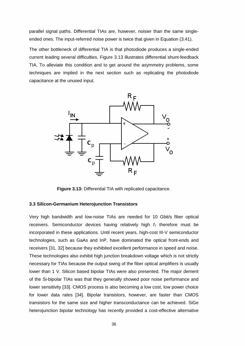
36
parallel signal paths. Differential TIAs are, however, noisier than the same single-
ended ones. The input-referred noise power is twice that given in Equation (3.41).
The other bottleneck of differential TIA is that photodiode produces a single-ended
current leading several difficulties. Figure 3.13 illustrates differential shunt-feedback
TIA. To alleviate this condition and to get around the asymmetry problems, some
techniques are implied in the next section such as replicating the photodiode
capacitance at the unused input.
Figure 3.13: Differential TIA with replicated capacitance.
3.3 Silicon-Germanium Heterojunction Transistors
Very high bandwidth and low-noise TIAs are needed for 10 Gbit/s fiber optical
receivers. Semiconductor devices having relatively high fT therefore must be
incorporated in these applications. Until recent years, high-cost III-V semiconductor
technologies, such as GaAs and InP, have dominated the optical front-ends and
receivers [31, 32] because they exhibited excellent performance in speed and noise.
These technologies also exhibit high junction breakdown voltage which is not strictly
necessary for TIAs because the output swing of the fiber optical amplifiers is usually
lower than 1 V. Silicon based bipolar TIAs were also presented. The major demerit
of the Si-bipolar TIAs was that they generally showed poor noise performance and
lower sensitivity [33]. CMOS process is also becoming a low cost, low power choice
for lower data rates [34]. Bipolar transistors, however, are faster than CMOS
transistors for the same size and higher transconductance can be achieved. SiGe
heterojunction bipolar technology has recently provided a cost-effective alternative

37
and higher integration levels, especially SiGe BiCMOS process, with improved
sensitivity for 10-Gbit/s fiber optical front-ends and for the development of
photoreceivers. One of the most important advantages of the SiGe BiCMOS
technology is that it enables analog and digital parts of the optical receiver to be
integrated in the same chip. In that case, output drivers and output impedance
matching networks are avoided. Since SiGe simultaneously enables high speed and
low power consumption, it has been becoming an important choice for the
realization of high speed fiber optical receivers.
SiGe BiCMOS applications range from wired and wireless communications circuits,
to disk storages, to high speed, high bandwidth instrumentation. The usage of
discrete SiGe HBTs and amplifiers in wireless devices is common place. In addition
to highly occupation in high speed 10-40 Gbit/s optical receivers, integrated
BiCMOS SiGe chips can be found in GSM, wireless LAN chipsets etc.
The concept of combining Silicon (Si) and Germanium (Ge) into an alloy for usage in
transistor engineering is an old one. However, because of difficulties in growing
lattice-matched SiGe alloy on Si, this concept is reduced to practical reality only in
the last 25 years [35]. SiGe HBT technology was originally developed at IBM.
However, that effort failed to CMOS, primarily because of its high power
consumption [35]. Figure 3.14 illustrates two base contacts NPN SiGe cross-section.
Figure 3.14: Cross-section of vertical NPN SiGe transistor.

38
A SiGe HBT is similar to a conventional Si bipolar transistor except for the base.
SiGe, a material with narrower bandgap than Si, is used as the base material. Ge
composition is typically graded across the base to create an accelerating electric
field for minority carriers moving across the base [36-40].
A direct result of the Ge grading in the base is higher speed, and thus higher
operating frequency. The transistor gain is also increased compared to a Si BJT,
which can then be traded for a lower base resistance, and hence lower noise. For
the same amount of operating current, SiGe HBT has a higher gain, lower RF noise,
and low 1/f noise than an identically constructed Si BJT [36]. The higher raw speed
can be traded for lower power consumption as well. One major drawback of the
SiGe is low junction break-down voltages. This specification limits the design
flexibility as given in the next section.
As stated above, the real strength of SiGe lies in its ability to integrate analog, RF
and digital architectures on a single package using existing CMOS fabs. This is not
possible with any other technologies such as GaAs etc [35].

39
4. DESIGN OF DIFFERENTIAL TRANSIMPEDANCE AMPLIFIER IN SiGe
BiCMOS FOR 10 Gbit/s FIBER OPTICAL RECEIVERS
This chapter presents a differential, low-noise transimpedance amplifier for 10 Gbit/s
fiber links using AMS 0.35 m SiGe HBT BiCMOS process, which is suitable for 10
Gbit/s photoreceivers. Circuit is realized in the ITU VLSI Laboratories using the
Cadence Design Environment tool.
At the beginning of the circuit design, transistors in the signal path are searched for
highest fT. At the collector current between 0.4-0.62 mA, the 12 μm length and 0.4
μm width emitter size SiGe exhibited largest fT (for the 2 base contacts vertical
SiGe). However, this result helped only to pay more attention to the dimensions and
bias currents. To get very good performance results, the emitter size of the
transistors (together with the other parameters for sure) were varied around these
dimensions. All components and parameters in the realized TIA are implemented in
RF models.
Apart from TIA design requirements widely discussed in the previous section, the
two major bottlenecks were avoided: First, BJTs had not to go into saturation region
even at highest input currents. Second, it had to be cared about low breakdown
voltages of junctions, which is 1 V for the base-emitter junction and 2 V for the
collector-emitter junction.
4.1 Circuit Design
As a first stage, TIA must have a very little group delay deviation from the low
frequencies up to high frequencies because time jitter caused by excessive group
delay variation cannot be compensated for at the succeeding stages. In contrast, a
drop in signal magnitude at higher frequencies can be improved by using PA after
the TIA. That being the case, lowering the group delay variation over the bandwidth
was one of the major issues during the design. This issue is mostly overcome by
obtaining and realizing Bessel type TIA. The advantage of Bessel response was
indicated in section three.
Figure 4.1 illustrates eye diagrams of Butterworth and Bessel TIAs. In this example,
NRZ of 10 Gbit/s PRBS signal is applied to the input of Butterworth and Bessel TIA

40
having 6 GHz bandwidth. As it is seen from the Figure 4.1, even with a bandwidth at
almost half the speed of the input signal, the Bessel TIA still has an open eye,
compared to that for a Butterworth TIA. The nature of the Bessel transfer function
makes it relatively immune to parasitic that can cause ringing. This is an advantage
for integrated circuit design, where the circuit parameters of the fabricated chip vary
from the ideal layout simulation.
Figure 4.1: Result of limited bandwidth on Bessel and Butterworth TIAs.
Since post amplifier is differential, the circuit satisfying differential operation must be
built. For single-ended output TIA, this might be done by applying reference voltage
to the one input of the PA and applying TIA output to the other input [41]. This
technique requires design of reference voltage generator. In other case, TIA can be
realized in differential architecture having differential outputs. The latter makes the
TIA immune to any common mode noise that it is preferred over the single-ended
structure. As stated before, however, the input-referred noise power of the
differential TIA is twice than that of the single-ended structure.
Cascode [42] and inductive peaking [43] techniques including active inductive
peaking [44] were the alternative choices to reach the desired bandwidth of the
transimpedance amplifier (around 8-9 GHz). Broadband operation, however, has
been succeeded without using these techniques. Common-emitter with shunt-

41
feedback resistor is included in the circuit because of its good performance over the
common-base structure, particularly in noise, dynamic range and low power
consumption.
Realized differential SiGe TIA schematic is shown in Figure 4.2. The PIN photodiode
with the intrinsic capacitance of 100 fF is modeled at the input of the circuit. Since
photodiode output is single-ended, current from the photodiode is directed to the
only one input of the TIA (T1). In this case, photodiode capacitance CP is replicated
at the other input (T2) to achieve fully symmetrical operation. This can be
accomplished during chip design by placing dummy photodiode to the unused input
of T2. Alternatively, by the help of the knowledge of the total capacitance (including
parasitic capacitances and if exits bond wire inductance) at the input of T1, the same
total impedance can be placed to the other input of the TIA [45]. The dominant pole
of the differential TIA is defined by the time constant at the input node. Shunt-
feedback resistors RF are applied around voltage amplifier to reduce input
impedance, which also reduces time constant at the input nodes allowing -3dB cut-
off frequency to be higher. Emitter followers (T3, T4, T5 and T6) are used for DC level
shifting and as buffer to drive next stages. The outputs are isolated from the
feedback networks in order to prevent transimpedance gain and bandwidth from
degradation because of the loading effect of the subsequent stage. Current mirrors
are incorporated in the circuit as loads in order to neglect high value resistors from
the circuit. All diode-connected transistors are needed for level shifting in order to
keep VCE less than breakdown voltage. Beta helper (T8) and emitter degeneration
resistors are used at the biasing circuit in order to improve current matching
performance of the current mirrors.

42
Figure 4.2: Realized differential SiGe TIA schematic.

43
Figure 4.3: Half-circuit model of the differential SiGe TIA with photodiode small-signal model.
To extract transfer function and noise equations, half-circuit model of the differential
TIA is used shown in Figure 4.3. The TIA has a voltage amplifier and a shunt-
feedback resistor RF. I3 and I5 are the current sources representing the current
mirrors. Voltage gain of the emitter follower at the last stage is assumed
approximately one. T1 and T3 are accepted as the same transistors. Voltage
amplifier is modeled with a single dominant pole. With the help of [10, 21, 46]
transimpedance ZT is
21
o effT
eff 'c ct t eff' F
F
A RZ s
Rs C R s C R
R
(4.1)
where
co mb
rA g R
r r
(4.2)

44
1
Feff
Fo
r RR
r A R
(4.3)
1p otC C C C A
(4.4)
2c µ cscR C C
(4.5)
' FF
F
R rR
R r
(4.6)
Where C is the base-collector capacitance; Ccs is the collector-substrate
capacitance and Ct is the total capacitance at the input of the TIA. rb is the intrinsic
base resistance; r and C base-emitter resistance and capacitance, respectively. Ao
is the open loop DC voltage gain. From (4.1), DC transimpedance gain RT is
oTin
oeff
vR A R
i
(4.7)
In a second order system, the damping factor must be equal to 3
2 in order to obtain
Bessel response which has a maximally flat group delay in the pass band. Using 3
2
in Equation (4.1), bandwidth of the TIA is
31 07
2o
dBteff
. Af
R C
(4.8)
This result mandates that bandwidth of the voltage amplifier must be a factor 3
larger than the unity-gain frequency of the open-loop response [21]. Since, input
transistors T1 and T2 are biased for highest fT, RC and RF are the major design
parameters to obtain maximally linear phase response. RF is also restricted by the
transimpedance gain and noise parameters. Since input impedance directly affects
stability of the TIA, HBT with 2 base contacts are chosen in order to make a
compromise between base resistance and base parasitic capacitance. RC and RF
are chosen as 900 and 150 , respectively. All circuit device values including
emitter sizes of transistors are provided in Table 4.1. Emitter width is fixed to 0.4 μm
for all HBTs and lengths are changed for the needed size. Table 4.2 gives DC
operating points of the transistors in the signal path. Small breakdown voltage of
collector-emitter junction is avoided even at the maximum input levels. Transient
node voltages are not more than 1.9 V when the input current is 400 μApp.

45
Table 4.1: Device values and transistor emitter sizes.
RF
900 Ω
RC
150 Ω
R1
830 Ω
R2
100 Ω
R3
15 Ω
R4
40 Ω
R5
40 Ω
R6
40 Ω
R7
40 Ω
CP
100 fF
Emitter Size
T1
2.4 μm2
T2
2.4 μm2
T3
4.8 μm2
T4
4.8 μm2
T5
4.8 μm2
T6
4.8 μm2
T7
4.8 μm2
T8
9.6 μm2
T9
9.6 μm2
T10
2.4 μm2
T11
4.8 μm2
T12
4.8 μm2
T13
4.8 μm2
T14
4.8 μm2
T15
4.8 μm2
T16
4.8 μm2
T17
4.8 μm2
T18
4.8 μm2
Table 4.2: Transistor biasing points.
T10
IC= 5.6 mA
VCE= 1.048 V
T1
IC= 2.8 mA
VCE=1.736 V
T2
IC= 2.8 mA
VCE= 1.736 V
T3
IC= 3.58 mA
VCE= 1.283 V
T4
IC= 3.58 mA
VCE= 1.283 V
T5
IC= 3.57 mA
VCE= 1.048 V
T6
IC= 3.57 mA
VCE= 1.048 V
Equivalent input-referred noise current spectrum in,in2
of the half-circuit can be
written as;
2 2 221 3 5
2 2 221
1
1
4 1 4 14 2
12n,in
p CbF
C
c
n
cm
n
c
i I vKT KTKTr sC q qI
f R R f fR R
v
g Z
(4.9)
Where
22 25
5 5 554
12 2 4n
e BC bv
qI Z qI ||Z KTrsCf
(4.10)
22 23
3 3 3 33
12 2 4n
C e BF Fb
vqI Z ||R qI ||Z KT( r
f)R
sC
(4.11)
k is the Boltzmann constant, T is the temperature in Kelvin and q is the electric
charge. 𝑣𝑛32 and 𝑣𝑛5
2 are the equivalent input-referred noise voltage generators at
the input of the T3 and T5, respectively. For entire circuit in,in2
is twice that given in
Equation (4.9). Dominant noise sources are base and collector shot noise sources
of the input transistors T1 and T2 (3rd and 4th terms in Equation (4.9)) and thermal
noise sources from RF feedback resistors and intrinsic base resistances rb (first and
second terms in Equation (4.9)). Since low frequency corner of fiber
communications is a couple of kHz, flicker and burst noise sources are neglected.

46
4.2. Simulation Results
Simulation is performed by using the technology of 0.35 SiGe HBT BiCMOS
process whose fT is about 70 GHz. Figure 4.4 shows differential transimpedance
gain of the SiGe TIA. Flat frequency response is achieved. Bandwidth is 9 GHz and
low frequency differential transimpedance gain is 57.93 dB (making 800 Ω which is
almost equal to RF). Figure 4.5 depicts group delay variation over the frequency.
Less than 1 ps change over the bandwidth is succeeded. These results coincide
with the theoretical calculations given above.
Figure 4.4: Differential transimpedance gain of the TIA.
106
108
1010
48
50
52
54
56
58
60
Frequency (Hz)
Tra
nsi
mp
ed
an
ce (
dB
-oh
m)
BW = 9.039
GHz

47
Figure 4.5: Group delay variation of the frequency response over the bandwidth.
Figure 4.6: Total input-referred noise current spectrum of the differential TIA.
106
108
1010
26
28
30
32
34
Frequency (Hz)
Gro
up
Dela
y (
ps)
105
106
107
108
109
1010
6.5
7
7.5
8
8.5
9
9.5
10
10.5
11
11.5
Frequency (Hz)
Ino
ise (
pA
/ s
qrt
(H
z)
)

48
Input-referred noise current spectrum is illustrated in Figure 4.6. Noise current is
below 7 pA/ Hz up to 1 GHz. It is less than 11 pA/ Hz between 1 GHz and 9 GHz.
Total integrated input-referred noise current 𝑖𝑛 ,𝑖𝑛 ,𝑡𝑜𝑡 is 1.061 A. 15 GHz noise
bandwidth is considered for 𝑖𝑛 ,𝑖𝑛 ,𝑡𝑜𝑡 because the realized circuit contains more poles
(second dominant pole is at the output of the voltage amplifier and the other one
from the common-collector stage). As expected, noise is dominated by base and
collector shot noise of T1 and T2 and thermal noise of the base resistances (66% of
the total noise). Feedback resistors RF contribute to the noise about 22%. Noise
percentage of each device is presented in Appendix A. Using the Equation (3.13),
sensitivity of the differential TIA at BER of 10-12 can be found as 15 App. by using
the Equation (3.24), averaged input noise current 𝑖𝑛 ,𝑖𝑛 ,𝑎𝑣𝑔 can be found as 11.18
pA / 𝐻𝑧. Maximum peak-to-peak input current of the TIA is 400 App. Although
linearity of the signal is preserved up to 1 mApp input current levels, higher peak-to-
peak currents than 400 App will cause VCE of the T1 and T2 to exceed collector-
emitter junction breakdown voltage.
Differential output waveforms of the TIA is depicted in Figure 4.7. The TIA is driven
with a NRZ data stream of 10 Gbit/s and 231-1 pseudo random bit sequence (PRBS)
with the amplitude of 15 App and 400 App, respectively. Very good signal shape
with little overshoot is obtained. Differential output swing for the first case is 12
mVpp. In the second case, maximum differential output swing is 320 mVpp.

49
(a)
(b)
Figure 4.7: Differential output waveform of the circuit. The input data stream is
NRZ 10 Gbit/s 231 -1 PRBS. (a) Input current is 15 App. (b) Input
current is 400 App.
1 1.5 2 2.5 3 3.5 4 4.5 5
x 10-9
-2
0
2
4
6
8
10
12
14x 10
-3
Time (s)
Dif
fere
nti
al
Ou
tpu
t (V
)
0 0.5 1 1.5 2 2.5 3 3.5 4 4.5 5
x 10-9
-0.05
0
0.05
0.1
0.15
0.2
0.25
0.3
0.35
Dif
fere
nti
al
Ou
tpu
t (V
)
Time (s)

50
Figure 4.8 illustrates single-ended output S22 parameter of the realized circuit. The
proposed differential TIA is intended for the integrated receiver compromising both
TIA and PA in a single chip. If differential TIA is not implemented in the single die
together with the PA, then TIA must have capability to drive 50 loads. Hence, 30
resistors are placed to the both outputs for impedance matching. S22 is less than
-15 dB over the bandwidth implying good matching. Adding matching resistors
sacrifices the midband transimpedance gain 5 dB loss per output.
Eye diagrams resulted in a wide eye opening shown in Figure 4.9. The TIA input is
fed with two input currents: 15 App and 300 App. The data stream is again 10
Gbit/s and 231 -1 PRBS. To demonstrate the eye diagram performance two
scenarios are realized: In the first case, outputs are loaded with 100 fF capacitors to
characterize the effect of the subsequent stage [47]. In the latter, 30 matching
resistors are added to the both outputs in case TIA has to drive 50 Ω transmission
line. The eye openings are clear for both horizontal and vertical openings.
Figure 4.8: Single-ended S22 parameter of the realized TIA. 30 resistors are
added to the both output for 50 matching.
104
105
106
107
108
109
1010
-22
-21
-20
-19
-18
-17
-16
-15
Frequency (Hz)
S2
2 (
dB
)

51
(a)
(b)
Figure 4.9: Eye diagrams showing differential output at 10 Gbit/s 231 - 1 PRBS
data stream. (a) Input current is 15 App, both outputs are loaded
with 100 fF capacitor. (b) Input current is 300 App, both outputs are
loaded with 100 fF capacitor. (c) Input current is 15 App, both
outputs are loaded with 50 resistors. (d) Input current is 300 App,
both outputs are loaded with 50 resistors. In the case of (c) and (d)
30 matching resistors are added to the both outputs.

52
(c)
(d)
Figure 4.9 (continued): Eye diagrams showing differential output at 10 Gbit/s 231 -
1 PRBS data stream. (a) Input current is 15 App, both outputs are loaded with 100 fF capacitor. (b) Input current
is 300 App, both outputs are loaded with 100 fF
capacitor. (c) Input current is 15 App, both outputs are
loaded with 50 resistors. (d) Input current is 300 App,
both outputs are loaded with 50 resistors. In the case
of (c) and (d) 30 matching resistors are added to the both outputs.

53
5. CONCLUSION
In this dissertation, the differential SiGe transimpedance amplifier for 10 Gbit/s fiber
optical receivers is realized and its results are presented. The TIA is optimized for
the best phase linearity over the bandwidth resulted in a group delay variation less
than 1 ps. No inductor is used to achieve wideband operation.
The differential structure of the TIA makes it immune to the effect of the supply and
substrate noise. Results are appreciable. In addition to flat frequency response, 9
GHz bandwidth is provided. Differential transimpedance gain is almost 58 dB. The
electrical sensitivity of the proposed TIA is 15 App. Power consumption is 71 mW
and maximum differential output swing is 320 mVpp. The figure-of-merit averaged
input-referred-noise current is 11.18 pA/ Hz. It has been demonstrated that the
differential TIA is well suited for 10 Gbit/s data rate and for OC-192 specifications.
Table 5.1 summarizes simulation performance of the realized circuit and makes
comparison to the some existing designs. III-V technologies such as GaAs and InP
have recently not preferred in the photoreceivers because they consume much more
power for the same speed. In reference [48] and [49], there are no noise and
sensitivity results, which are very important for a low-noise front-end preamplifier.
CMOS has lower transimpedance for the same speed [50]. In [48], although more
than 10 GHz bandwidth is achieved, noise performance is not provided. As widely
discussed in this thesis, as the bandwidth of the TIA is increased pointlessly, the
noise issue will be a big bottleneck for a transimpedance amplifier.
The first goal when realizing an optical receiver must be to integrate all of the analog
and digital blocks in the same package as well as preserving high performance and
reducing production expenses.
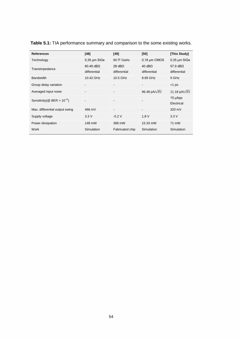
54
Table 5.1: TIA performance summary and comparison to the some existing works.
References [48] [49] [50] [This Study]
Technology 0,35 μm SiGe 60 fT GaAs 0,18 μm CMOS 0,35 μm SiGe
Transimpedance 60.49 dBΩ
differential
28 dBΩ
differential
40 dBΩ
differential
57.9 dBΩ
differential
Bandwidth 10.42 GHz 10.5 GHz 8.69 GHz 9 GHz
Group delay variation - - - <1 ps
Averaged input noise - - 96.48 pA/ 𝐻𝑧 11.18 pA/ 𝐻𝑧
Sensitivity(@ BER = 10-12
) - - - 15 μApp
Electrical
Max. differential output swing 466 mV - - 320 mV
Supply voltage 3.3 V -5.2 V 1.8 V 3.3 V
Power dissipation 148 mW 368 mW 15.33 mW 71 mW
Work Simulation Fabricated chip Simulation Simulation

55
REFERENCES
[1] Gao, J. (2011). Optoelectronic Integrated Circuit Design and Device Modeling, Jon Wiley & Sons Pte Ltd, Shanghai, China.
[2] Agrawal, G. P. (2010). Fiber-Optic Communication Systems, The Institute of Optics, Jon Wiley & Sons Inc, University of Rochester, Rochester, New York, USA.
[3 Buchwald , A., Martin, K. W. (1994). Integrated Fiber-Optic Receivers, Kluwer Academic Publishers, Boston, USA.
[4] Suzaki, T., Soda, M., Takenori M., Tezuka, H., Ogawa, C., Fujita, S., Takemura, H., Tashiro, T. (1992). A Si Bipolar Chip Set for 10Gb/s Optical Receiver, IEEE 39th Solid-State Circuits Conference, pp: 100-101.
[5] Seng, C. W., Sern, T. Y., Seng, Y. K. (2013). A low power wideband differential
transimpedance amplifier for optical receivers in 0.18 μm CMOS, IEEE 11th International Conference on New Circuits and Systems (NEWCAS), pp: 1-4.
[6] <https://learningnetwork.cisco.com/thread/4414> date retrieved 01.10.2013.
[7] Bishnu, P. P. (2006). Guided Wave Optical Components and Devices, Indian Institute of Technology, Elsevier Academic Press, Amsterdam, Holland.
[8] Dries, J.C., Bush, M.G., Lange, M., Brubaker, R.M., Mykietyn, E., Cohen, M.J., Olsen, G.H. (2000). Demonstration of a 40 Gb/s, 4 Channel Optical Receiver Array, IEEE 13th Annual Meeting on Lasers and Electro-Optics Society (LEOS), 2000, vol 1, pp: 344-345.
[9] Prasad S, Schumacher, H., Gobinath, A. (2009). High-Speed Electronic and Optoelectronics, Cambridge University Press, Cambridge, England.
[10] Sackinger, E. (2005). Broadband circuits for optical fiber communication. Wiley-Interscience. New Jersey, USA.
[11] Graeme, J. G. (1995). Photodiode Amplifiers, McGraw Hill, Boston, USA.
[12] Jung, D.Y., Park, S.H., Lee, K.H., Chang, W.J., Nam, E.S., Lim, J.W., Park, C.S. (2002). An InGaP/GaAs HBT transimpedance amplifier for 10 Gb/s optical communication. IEEE 3rd International Conference on Microwave and Millimeter Wave Technology (ICMMT), pp: 974-977.
[13] Fukuyarna, H., Murata, K., Sano, K., Kitabayashi, H., Yamane, Y., Enoki, T., Sugahara, H. (2003). Optical receiver module using an InP HEMT transimpedance amplifier for over 40 Gbit/s. IEEE Gallium Arsenide Integrated Circuit Symposium, 25th Annual Technical Digest, pp: 237-240.
[14] Tang, W., Plant, D. V. (2006). A low power 3.125Gb/s/Channel parallel optical receiver for very short reach applications. IEEE 23rd Biennial Symposium on Communications, pp: 35-38.

56
[15] Li, C., Palermo, S. (2013). A Low-Power 26-GHz Transformer-Based Regulated Cascode SiGe BiCMOS Transimpedance Amplifier, IEEE Journal of Solid-State Circuits, vol: 48, issue 5, pp: 1264-1275.
[16] Ramaswami, R., Sivarajan, K. N. (2002). Optical Networks: A Practical Perspective, Morgan Kaufmann Publishers, San Fransisco, USA.
[17] Noe, R. (2010). Essentials of Modern Optical Fiber Communications, Springer, Heilderberg, Germany.
[18] Nishimoto, H., Okiyama, T., Kuwata, N., Arai, Y., Miyauchi, A. and Touge, T. (1988). New Method of analyzing eye patterns and its application to high speed optical transmission Systems, IEEE Journal of Lightwave Technology, vol:6, issue 5, pp: 678-685.
[19] Razavi, B. (2003). Design of Integrated Circuits for Optical Communications, McGraw-hill, Los Angeles, USA.
[20] Muller, P., Leblebici, Y. (2007). CMOS Multichannel Single-Chip Receivers for Multi-Gigabit Optical Data Communications, Springer, Eton, Switzerland.
[21] Hermans, C., Steyaert, M. (2007). Broadband Opto-Electrical Receivers in Standard CMOS, Springer, Dordrecht, The Netherlands.
[22] Maas, S. A. (2005). Noise in Linear and Nonlinear Circuits, Artech House, Boston, USA.
[23] Gray, P. R., Hurst, P.J., Lewis, S. H., Meyer, R. G. (2006). Analaysis and Design of Analog Integrated Circuits, John Wiley, New York, USA.
[24] Nguyen, D. B., Le, Q., Le, Y., Le. H. and Lee, S. (2005). A High Linearity, Efficient Bandwidth, and High Stability Transimpedance Amplifier, 48th Midwest Symphosium on Circuits and Systems (MWSCAS), vol: 1, pp: 167-170.
[25] Schneider, K., Zimmermann, H. (2006). High Sensitive Optical Receivers, Springer, Heilderberg, Germany.
[26] Vanisri, T., Toumazou, C. (1995), Integrated High Frequency Low-Noise Current-Mode Optical Transimpedance Preamplifiers: Theory and Practice, IEEE Journal of Solid-State Circuits, vol: 30, isuue 6, pp: 677-685.
[27] Dorf, R. C., Bishop, R. H. (1988). Modern Control Systems, Addison-Wesley, Boston, MA, USA.
[28] Neuhauser, M., Rein, H., Wernz, H. (1996). Low-Noise, High-Gain Si-Bipolar Preamplifiers for 10 Gb/s Optical-Fiber Links Design and Realization, IEEE Journal of Solid-State Circuits, vol: 31, issue 1, pp: 24-29.
[29] Kang, S. S., Leblebici, Y. (1999). CMOS Digital Integrated Circuits, McGraw Hill, Boston, USA.
[30] Hodges, D. A., Jackson, H. G. (1988). Analysis and Design of Digital Integrated Circuits, McGraw Hill, New York, USA.
[31] Jiang, F., Chen , J., Wu, D., Wu J., Jin, Z., Liu, X. (2012). A wide dynamic range transimpedance amplifier with high gain-bandwidth product for 10 Gb/s optical links, IEEE International Workshop on Microwave and Milimeterwave Circuits and Systems Technology (MMWCST), pp: 1-4.

57
[32] Fields, C.H., Tsen, T., McGuire, C., Yoon, Y., Zehnder, D., Thomas, S., Montes, M., Valles, I., Duvall, J., Hussain, T. (2010). 110+ GHz Transimpedance Amplifier in InP-HBT Technology for 100 Gbit Ethernet, IEEE Microwave and Wireless Components Letters, vol: 20, issue: 8, pp: 465-467.
[33] Ohhata, K., Masuda, T., Imai, K., Takeyari, R., Washio, K. (1999). A wide-dynamic-range, high-transimpedance Sibipolar preamplifier IC for 10-Gb/s optical fiber links, IEEE Journal of Solid-State Circuits, vol: 34, issue: 1, pp: 18-24.
[34] Liu, F.Y., Patil, D., Lexau, J., Amberg, P., Dayringer, M., Gainsley, J., Moghadam, H.F., Zheng, X., Cunningham, J.E., Krishnamoorthy, A.V., Alon, E., Ho, R. (2012). 10-Gbps, 5.3-mW Optical Transmitter and Receiver Circuits in 40-nm CMOS, IEEE Journal of Solid-State Circuits, vol: 47, issue: 9, pp: 2049-2067.
[35] <http://www.eng.auburn.edu/~guofu/sige_intro.htm> date retrieved 03.08.2013.
[36] Ashburn, P. (2003). SiGe Heterojunction Bipolar Transistors, John Wiley & Sons Ltd, University of Southampton, Southampton, UK.
[37] Cressler, J. D., Niu, G. (2003). Silicon-Germanium Heterojunction Bipolar Transistors, Artech House, Boston, USA.
[38] Rieh, S. J., (2002). SiGe HBTs with Cut-off Frequency of 350 GHz, IEEE ınternational on Electron Devices Meeting (IEDM), pp.771-774.
[39] Kasper, E., and Paul D. J. (2005). Silicon Quantum Integrated Circuits, Springer.
[40] Zeghbroeck, V. B., 2008. Principles of Semiconductor Devices and Heterojunctions, Prentice Hall, Boston, USA.
[41] Vatannia, S., Yeung, P. and Lu, C. (2005). A Fast Response 155-Mb/s Burst-Mode Optical Receiver for PON. IEEE Photonics Technology Letters, vol: 17, no. 5, pp: 1067-1069.
[42] Rieh, J.-S., Qasaimeh, O., Klotzkin, D., Lu, L.-H., Yang, K., Katehi, L.P.B., Bhattacharya, P., Croke, E.T. (1997). Monolithically Integrated SiGe/Si PIN HBT Front-End Transimpedance Photoreceivers. IEEE/Cornell Conference on Advanced Concepts in High Speed Semiconductor Devices and Circuits, Page(s): 322 – 331.
[43] Jin, J. D., Hsu, S., (2008). A 75-dB 10-Gb/s Transimpedance Amplifier in
0.18-m CMOS Technology, IEEE Photonics Technology Letters, vol: 20, issue: 24, pp: 2177 – 2179.
[44] Han, L., Yu, M., Zong, L. (2010). Bandwidth Ehancement for Transimpedance Ampilfier in CMOS Process. IEEE 3rd International Conference on Biomedical Engineering and Informatics (BMEI), vol: 7, pp: 2839 – 2842.
[45] Kim, H. H., Chandrasekhar, S., Burrus, C. A. and Bauman, J. (2001). A Si BiCMOS transimpedance amplifier for 10-Gb/s SONET receiver. IEEE Journal of Solid-State Circuits, SC 6(5):769-776.
[46] EL-Diwany, M. H., Roulston, D. J., Chamberlain S. G. (1981). Design of low-noise bipolar transimpedance preamplifiers for optical receivers. IEE Proc. G, Electron. Circ. & Syst., 128, pp: 299-305.

58
[47] Samadi, M. R., Karsilayan, A. I. and Silva-Martinez, J. (2002). Design of Transimpedance and Limiting Amplifiers for 10 Gb/s Optical Communication Systems. IEEE 45th Midwest Symposium on Circuits and Systems (MWSCAS), vol: 3, pp: 164-167.
[48] Fenfei H., Jingxing D. (2008). 0.35 m SiGe BiCMOS Front-End Amplifier For 10Gb/s Optical Receiver. IEEE International Conference on Microwave and Millimeter Wave Technology (ICMMT), pp: 249 – 252.
[49] Zhou L., Wu D., Wu J., Jin Z., and Liu X. (2012). Design of a 10GHz Bandwidth Variable Gain Amplifier using a GaAs HBT Technology. IEEE International Workshop on Microwave and Millimeter Wave Circuits and System Technology (MMWCST), pp: 1-4.
[50] Huang T., Zhang Q., Zhang W. (2011). A Novel Transimpedance Amplifier for 10 Gbit/s Optical Communication System. IEEE 9th International Conference on ASIC, ASICON, pp: 843 – 846.

59
APPENDICES
APPENDIX A: Program Schematic and Relevant Figures.

60

61
Figure A.1: Program schematic of realized TIA.

62
Figure A.2: Simulation and values.

63
Figure A.3: Noise contribution of each device.

64

65
CURRICULUM VITATE
Name Surname: Yunus AKBEY
Place and Date of Birth: Ġstanbul, 1982
Address: Esenyurt, Ġstanbul
E-Mail: [email protected]
B.Sc.: Department of Avionics, Faculty of Aeronautics and
Astronautics, Anadolu University
Professional Experience:
Yunus Akbey received the B.Sc. degree from the Department of Avionics, at
Anadolu University in 2006. His research interests are microwave and RF circuit
design, design of analog IC topologies.
List of Publications Papers:
Akbey, Y., Palamutçuoğulları, O. (2013). A Broadband, Differential
Transimpedance Amplifier in 0.35 μm SiGe BiCMOS Technology for 10 Gbit/s
Fiber Optical Front-Ends. Journal of Analog Integrated Circuits and Signal
Processing, Springer, vol: 74, issue: 1, pp: 155-162.
List of Conferences Papers:
Akbey, Y., Palamutcuogulları, O. (2011). 9 GHz Differential SiGe
Transimpedance Amplifier for 10 Gbit/s Fiber Optical Front-Ends. 7th
International Conference on Electrical and Electronics Engineering (ELECO),
pp. II-250–II-254.