isolated, regulated dc-dc converter - vicor corporation · 2018-04-24 · b1 ft digital output...
TRANSCRIPT

HDC Module Rev C vicorpower.comPage 1 of 20 5/2014 800 927.9474
HDC Module
Isolated, Regulated DC-DC Converter
PRELIMINARY
HDC 300 B 120 x 400 y-00
Part Number Designation
300 = 180 - 420 Vdc L = Flanged baseplateN = Flangeless baseplate
HDC = HDConverter
Family
B Series
Model Input Voltage PackageOutput Voltage(Nom.) x10
TemperatureGrade
Power Pin /Base - Rev / Var
HDC 300 B 120 x 400 L - 00
120 = (VOUT
nominal) x 10
C = -20°C > TSTG > 100°C, -20°C > TJ > +125°CT = -40°C > TSTG > 100°C, -40°C > TJ > +125°CM = -65°C > TSTG > 100°C, -55°C > TJ > +125°C
Features
• Isolated , regulated DC-to-DC converter
• Up to 400 W, 33.3 A continuous
• 93.2 % peak efficiency
• 128 W/in2 power density
• Wide input range 180 to 420 Vdc
• ZVS high frequency (MHz) switching
n Enables low profile, high-density filtering
• Full operation during current limit
• OV, OC, UV, short circuit and thermal protection
• Through-hole Brick Package
Overview
• Part of the new HD Series of power conversion products
• Companion models to HDR Regulator Family
• Input Voltage: 180 to 420 Vdc
• Output: 12 Vdc
• Output Current to 33.3 Amperes
• Agency approvals: CE Mark
Product Overview
The HDC Isolated, Regulated DC Converter is a DC-to-DCconverter, operating from an unregulated, wide range input togenerate an isolated 12 Vdc output. With its high frequency zerovoltage switching (ZVS) topology, the HDC consistently delivershigh efficiency across the input line range. Modular HDC anddownstream DC-DC products support efficient powerdistribution, providing superior power system performance andconnectivity from a variety of unregulated power sources to thepoint-of-load.
400 = Max ratedoutput power
00 = ModuleCB = Evaluation Board

PRELIMINARY
HDC Module Rev C vicorpower.comPage 2 of 20 5/2014 800 927.9474
HDC 300 B 120 x 400 y-00
Typical Application
HDC
+IN
-IN
+OUT
-OUT
ZVSBuck
HDR
3.3, 5, 12 & 15 VOUT
12 V
3.3, 5, 12 & 15 VOUT

PRELIMINARY
HDC Module Rev C vicorpower.comPage 3 of 20 5/2014 800 927.9474
HDC 300 B 120 x 400 y-00
1 2
A
B
C
D
E
A’
B’C’
D’E’
F’G’
H’I’
J’
K’
Pin Configuration
Pin Descriptions
PinNumber
Signal Name Type Function
A1 +IN INPUT POWER Positive input power terminal
B1 FT DIGITAL OUTPUT Fault indicator
C1 PC DIGITAL INPUT Primary control
D1 NC NO CONNECTION Do not connect to this pin
E1 -IN INPUT POWER Negative input power terminal
A’2 +OUT OUTPUT POWER Positive output power terminal
B’2, D’2 NC NO CONNECTION Do not connect to this pin
C’2 +S OUTPUT POWER Positive remote sense
E’2 VDD OUTPUT POWER 3.3 V regulated voltage source for trimming
F’2 VDDB INPUT POWER Semi-regulated voltage for future use
G’2 TR ANALOG INPUT VOUT trim reference to SGND
H’2 FB DIGITAL OUTPUT Feedback PWM pulses for master-slave array for future use
I’2 -S OUTPUT POWER Negative remote sense
J’2 SGND GROUND Signal ground
K’2 -OUT OUTPUT POWER Negative output power terminal

PRELIMINARY
HDC Module Rev C vicorpower.comPage 4 of 20 5/2014 800 927.9474
HDC 300 B 120 x 400 y-00
Absolute Maximum Ratings
Parameter Rating Unit Notes
+In to –In voltage -0.5 to 550 Vdc 550 for 100 ms
FT to –In -0.5 to 3.6 Vdc
PC to –In voltage -0.5 to 3.3 Vdc
+Out to –Out voltage, +S to -Out -0.5 to 13.2 Vdc Externally applied
VDD to -Out -0.5 to 3.6 Vdc
VDDB to -Out -0.5 to 17.6 Vdc
TR to -Out -0.5 to 3.6 Vdc
FB to -Out -0.5 to 3.6 Vdc
Operating Temperature -55 to +125 °C M-Grade
Storage Temperature -65 to +125 °C M-Grade
Mounting torque 5 (0.57) in / lbs (N-M) 4 each
PRELIMINARY
HDC Module Rev C vicorpower.comPage 5 of 20 5/2014 800 927.9474
HDC 300 B 120 x 400 y-00
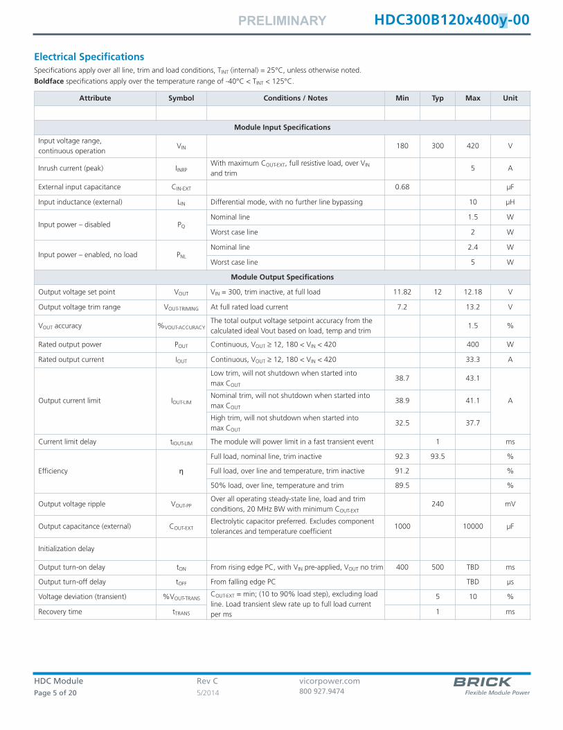
Electrical SpecificationsSpecifications apply over all line, trim and load conditions, TINT (internal) = 25°C, unless otherwise noted.
Boldface specifications apply over the temperature range of -40 °C < TINT < 125 °C.
Attribute Symbol Conditions / Notes Min Typ Max Unit
Module Input Specifications
Input voltage range,continuous operation
VIN 180 300 420 V
Inrush current (peak) IINRPWith maximum COUT-EXT, full resistive load, over VIN
and trim 5 A
External input capacitance CIN-EXT 0.68 µF
Input inductance (external) LIN Differential mode, with no further line bypassing 10 µH
Input power – disabled PQ
Nominal line 1.5 W
Worst case line 2 W
Input power – enabled, no load PNL
Nominal line 2.4 W
Worst case line 5 W
Module Output Specifications
Output voltage set point VOUT VIN = 300 , trim inactive, at full load 11.82 12 12.18 V
Output voltage trim range VOUT-TRIMING At full rated load current 7.2 13.2 V
VOUT accuracy %VOUT-ACCURACYThe total output voltage setpoint accuracy from thecalculated ideal Vout based on load, temp and trim
1.5 %
Rated output power POUT Continuous, VOUT ≥ 12 , 180 < VIN < 420 400 W
Rated output current IOUT Continuous, VOUT ≥ 12 , 180 < VIN < 420 33.3 A
Output current limit IOUT-LIM
Low trim, will not shutdown when started intomax COUT
38.7 43.1
ANominal trim, will not shutdown when started intomax COUT
38.9 41.1
High trim, will not shutdown when started intomax COUT
32.5 37.7
Current limit delay tIOUT-LIM The module will power limit in a fast transient event 1 ms
Efficiency ηFull load, nominal line, trim inactive 92.3 93.5 %
Full load, over line and temperature, trim inactive 91.2 %
50% load, over line, temperature and trim 89.5 %
Output voltage ripple VOUT-PPOver all operating steady-state line, load and trimconditions, 20 MHz BW with minimum COUT-EXT
240 mV
Output capacitance (external) COUT-EXTElectrolytic capacitor preferred. Excludes componenttolerances and temperature coefficient
1000 10000 µF
Initialization delay
Output turn-on delay tON From rising edge PC, with VIN pre-applied, VOUT no trim 400 500 TBD ms
Output turn-off delay tOFF From falling edge PC TBD µs
Voltage deviation (transient) %VOUT-TRANSCOUT-EXT = min; (10 to 90% load step), excluding loadline. Load transient slew rate up to full load currentper ms
5 10 %
Recovery time tTRANS 1 ms

PRELIMINARY
HDC Module Rev C vicorpower.comPage 6 of 20 5/2014 800 927.9474
HDC 300 B 120 x 400 y-00
Electrical Specifications (cont.)Specifications apply over all line, trim and load conditions, TINT (internal) = 25°C, unless otherwise noted.
Boldface specifications apply over the temperature range of -40 °C < TINT < 125 °C.
Attribute Symbol Conditions / Notes Min Typ Max Unit
Powertrain Protection
VIN undervoltage threshold VIN-UVLO- 125 155 V
VIN undervoltage recovery threshold VIN-UVLO+ 177 V
VIN overvoltage threshold VIN-OVLO+ 455 V
VIN overvoltage recovery threshold VIN-OVLO- 423 V
Overtemperature threshold (internal) TINT-OVP 125 °C
Short circuit, or temperature faultrecovery time
tFAULT 1 s

PRELIMINARY
HDC Module Rev C vicorpower.comPage 7 of 20 5/2014 800 927.9474
HDC 300 B 120 x 400 y-00
Signal SpecificationsAll specifications valid at 100% rated load and over specified input voltage range at 25°C, unless otherwise indicated.
Boldface specifications apply over the temperature range of -40 °C < TINT < 125 °C.
Fault: FT
• The fault pin is the Fault flag pin.
• When the module is enabled and no fault is present, the FT pin does not have current drive capability.
• Whenever the powertrain stops (due to a fault protection or disabling the module by pulling PC low), the FT pin outputs VDD and provides currentto drive an external circuit.
• When the module starts up, the FT pin is pulled high to VDD during microcontroller initialization and will remain high until soft start process starts
SIGNAL TYPE STATE ATTRIBUTE SYMBOL CONDITIONS / NOTES MIN TYP MAX UNIT
DIGITAL
INPUT
FT InactiveInternally generated VDD 3.21 3.3 3.39 V
FT internal pull upresistance to VDD
RFAULT-INACTIVE 9.5 10.0 10.5 kΩ
FT Active
FT Voltage VFAULT-ACTIVE At load = 4 ma 3.0 V
FT current drive capability IFAULT-ACTIVEOver-current FT drive beyond its capabilitymay cause module damage
4 mA
FT response time
tRESPONSE-FAULT After fault detected 200 µs
tRESPONSE-TIME After PC being pulled low 5 µs
tRESPONSE-TIME1
After the module returns to no fault state,the time for FT to become inactive, for inputUVLO and OVLO
1 ms
tRESPONSE-TIME2
After the module returns to no fault state,the time for FT to become inactive, for other(slower recovery) fault types
1 ms
Primary Control: PC
• The PC pin enables and disables the converter; when held low the unit will be disabled.• The PC pin has an internal pull-up to VDD and is referenced to the –IN pin of the converter.
SIGNAL TYPE STATE ATTRIBUTE SYMBOL CONDITIONS / NOTES MIN TYP MAX UNIT
DIGITAL
INPUTAny
PC enable threshold VPC-EN 2.31 V
PC disable threshold VPC-DIS 0.99 V
Internally generated VDD VDD 3.21 3.3 3.39 V
PC internal pull up
resistance to VDD
RENABLE-INT Pull up to VDD 9.5 10.0 10.5 kΩ

PRELIMINARY
HDC Module Rev C vicorpower.comPage 8 of 20 5/2014 800 927.9474
HDC 300 B 120 x 400 y-00
Signal SpecificationsAll specifications valid at 100% rated load and over specified input voltage range at 25°C, unless otherwise indicated.
Boldface specifications apply over the temperature range of -40 °C < TINT < 125 °C.
Regulated Voltage: VDD
• Regulated supply power• Intended to be used as low current supply for ancillary circuits
SIGNAL TYPE STATE ATTRIBUTE SYMBOL CONDITIONS / NOTES MIN TYP MAX UNIT
POWER
OUTPUT
Regular
Operation
VDD Voltage output VVDD_OUT 3.23 3.30 3.37 V
VDD Source current IVDD_OUT 20 mA
Semi-regulated Voltage: VDDB
• Unregulated supply power input, required for future products
SIGNAL TYPE STATE ATTRIBUTE SYMBOL CONDITIONS / NOTES MIN TYP MAX UNIT
POWER
INPUT
Regular
Operation
VDDB Voltage VVDDB 4 16 V
VDDB Currentconsumption
IVDDB VDD pin not loaded 18 30 mA
Feedback: FB
• PWM voltage regulation feedback from Digital Supervisor to DCM• Intended to be used for a parallel array (future option)
SIGNAL TYPE STATE ATTRIBUTE SYMBOL CONDITIONS / NOTES MIN TYP MAX UNIT
DIGITAL
OUTPUT
Regular
Operation
FB Peak Voltage VFB 3.3 3.37 V
PWM Frequency FPWM 25 kHz
FB PWM Duty Cycle DCFB 1 97 %
Trim: TR
• The TR pin enables and disables trim functionality when VIN is applied to the HDC. TR pin voltage is sampled right before soft start stage during startup
• If TR is not floating at power up and has a voltage less than TR trim enable threshold, trim is active
• If trim is active, the TR pin provides dynamic trim control with at least 500 Hz of -3 dB control bandwidth over the output voltage of the HDC
• The TR pin has an internal pull-up to VDD and is referenced to SGND pin of the converter
SIGNAL TYPE STATE ATTRIBUTE SYMBOL CONDITIONS / NOTES MIN TYP MAX UNIT
ANALOG
INPUT
Regular
Operation
FB Peak Voltage VFB 3.15 V
PWM Frequency FPWM 3.20 V
ANALOG
INPUT
Operational
with Trim
enabled
Internally generated VDD VDD 3.23 3.30 3.37 V
TR pin analog range VTRIM-RANGE 0 2.486 3.1 V
VOUT step resolution VOUT-RES With VDD = 3.3 V 6.21 mV
TR internal pull upresistance to VDD
RTRIM-INT 5.105 5.11 5.115 kΩ

PRELIMINARY
HDC Module Rev C vicorpower.comPage 9 of 20 5/2014 800 927.9474
HDC 300 B 120 x 400 y-00
Block Diagram
+IN
-IN
FT
PC
+OUT
-OUT
+S
-S
VDD
TR
VDDB
SGND
FB
DigitalSupervisor
DISO
VDD
TRIM
+S
-S
SGND
VDDB
VSP
+OUT
-OUT
+IN
-IN
DCMFT
PC
SEC-IN-A
SEC-COM
PRI-OUT-A
PRI-COM
PRELIMINARY
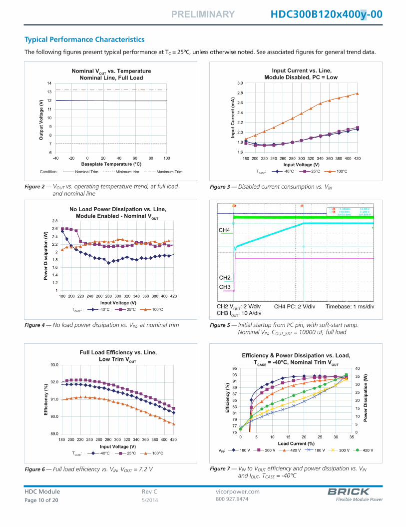
HDC Module Rev C vicorpower.comPage 10 of 20 5/2014 800 927.9474
HDC 300 B 120 x 400 y-00
Pow
er D
issi
patio
n (W
)
Input Voltage (V)
-40°C 25°C 100°CTCASE:
No Load Power Dissipation vs. Line,Module Enabled - Nominal VOUT
1
1.2
1.4
1.6
1.8
2
2.2
2.4
2.6
2.8
180 200 220 240 260 280 300 320 340 360 380 400 420
Figure 4— No load power dissipation vs. VIN, at nominal trim
Out
put V
olta
ge (V
)
Baseplate Temperature (°C)
Nominal VOUT vs. TemperatureNominal Line, Full Load
Nominal Trim Minimum trim Maximum TrimCondition:
6
7
8
9
10
11
12
13
14
-40 -20 0 20 40 60 80 100
Figure 2— VOUT vs. operating temperature trend, at full loadand nominal line
Inpu
t Cur
rent
(mA
)
Input Voltage (V)
Input Current vs. Line,Module Disabled, PC = Low
-40°C 25°C 100°CTCASE:
1.6
1.8
2.0
2.2
2.4
2.6
2.8
3.0
180 200 220 240 260 280 300 320 340 360 380 400 420
Figure 3— Disabled current consumption vs. VIN
Effic
iienc
y (%
)
Input Voltage (V)
Full Load Efficiency vs. Line,Low Trim VOUT
-40°C 25°C 100°CTCASE:
89.0
90.0
91.0
92.0
93.0
180 200 220 240 260 280 300 320 340 360 380 400 420
Figure 6— Full load efficiency vs. VIN, VOUT = 7.2 V
Efficiency & Power Dissipation vs. Load,TCASE = -40°C, Nominal Trim VOUT
Load Current (%)
Effic
ienc
y (%
)
Pow
er D
issi
patio
n (W
)
180 V 300 V 420 VV :IN 180 V 300 V 420 V
0
5
10
15
20
25
30
35
40
75 77 79 81 83 85 87 89 91 93 95
0 5 10 15 20 25 30 35
Figure 7— VIN to VOUT efficiency and power dissipation vs. VINand IOUT, TCASE = -40°C
Figure 5— Initial startup from PC pin, with soft-start ramp.Nominal VIN, COUT_EXT = 10000 uF, full load
Typical Performance Characteristics
The following figures present typical performance at TC = 25ºC, unless otherwise noted. See associated figures for general trend data.

PRELIMINARY
HDC Module Rev C vicorpower.comPage 11 of 20 5/2014 800 927.9474
HDC 300 B 120 x 400 y-00
Effic
iienc
y (%
)
Input Voltage (V)
Full Load Efficiency vs. Line,High Trim VOUT
-40°C 25°C 100°CTCASE:
91.0
92.0
93.0
94.0
180 200 220 240 260 280 300 320 340 360 380 400 420
Figure 10— Full load efficiency vs. VIN, VOUT = 13.2 V
Effic
iienc
y (%
)
Input Voltage (V)
Full Load Efficiency vs. Line,Nominal Trim VOUT
-40°C 25°C 100°CTCASE:
91.0
91.5
92.0
92.5
93.0
93.5
180 200 220 240 260 280 300 320 340 360 380 400 420
Figure 8— Full load efficiency vs. VIN, VOUT = 12 V
Efficiency & Power Dissipation vs. Load,TCASE = 25°C, Nominal Trim VOUT
Load Current (%)
Effic
ienc
y (%
)
Pow
er D
issi
patio
n (W
)
180 V 300 V 420 VV :IN 180 V 300 V 420 V
0
5
10
15
20
25
30
35
40
75 77 79 81 83 85 87 89 91 93 95
0 5 10 15 20 25 30 35
Figure 9— VIN to VOUT efficiency and power dissipation vs. VINand IOUT, TCASE = 25°C
Figure 12— 10% to 100% load transient response, VIN = 300 V,nominal trim, COUT_EXT = 1000 µF
Figure 13— 100% to 10% load transient response, VIN = 300 V,nominal trim, COUT_EXT = 1000 µF
Efficiency & Power Dissipation vs. Load,TCASE = 100°C, Nominal Trim VOUT
Load Current (%)
Effic
ienc
y (%
)
Pow
er D
issi
patio
n (W
)
180 V 300 V 420 VV :IN 180 V 300 V 420 V
0
5
10
15
20
25
30
35
40
45
75 77 79 81 83 85 87 89 91 93 95
0 5 10 15 20 25 30 35
Figure 11— VIN to VOUT efficiency and power dissipation vs. VINand IOUT, TCASE = 100°C
Typical Performance Characteristics (Cont.)
The following figures present typical performance at TC = 25ºC, unless otherwise noted. See associated figures for general trend data.

PRELIMINARY
HDC Module Rev C vicorpower.comPage 12 of 20 5/2014 800 927.9474
HDC 300 B 120 x 400 y-00
Figure 14— Typical output voltage ripple, VIN = 300 V, VOUT = 12 V,COUT_EXT = 1000 µF, full load
Typical Performance Characteristics (Cont.)
The following figures present typical performance at TC = 25ºC, unless otherwise noted. See associated figures for general trend data.

PRELIMINARY
HDC Module Rev C vicorpower.comPage 13 of 20 5/2014 800 927.9474
HDC 300 B 120 x 400 y-00
General CharacteristicsSpecifications apply over all line, trim and load conditions, TINT (internal) = 25°C, unless otherwise noted.
Boldface specifications apply over the temperature range of -40 °C < TINT < 125 °C.
Attribute Symbol Conditions / Notes Min Typ Max Unit
Mechanical
Length L Flanged and flangeless baseplate 56.62 / [2.23] 57.00 / [2.24] 57.39 / [2.26]
mm/[in]Width WFlanged baseplate 46.12 / [1.82] 46.50 / [1.83] 46.88 / [1.85]
Flangeless baseplate 34.61 / [1.36] 34.99 / [1.38] 35.37 / [1.39]
Height H Flanged and flangeless baseplate 15.36 / [0.61] 16.00 / [0.63] 16.36 / [0.66]
Volume VolFlanged baseplate 43.00 / [2.63]
cm3/[in3]Flangeless baseplate 35.56 / [2.17]
Weight W 100 / [3.53] g/[oz]
Pin material C145 copper, ½ hard
µinUnderplate Nickel 50 100
Pin finish Pure matte tin, whisker resistant chemistry 200 400
Assembly
Storage temperature TST -65 125 °C
ESD rating
HSMMethod per Human Body Model TestJEDEC JESD22-A114C
CLASS 1C
V
CDMCharged Device Model TestJEDEC JESD22-C101C
Reliablity
MTBF
Calculated per Telcordia TR-NT-000332,25°C
3.58 MHrs
Telcordia Issue 2 - Method I Case 3;25°C Ground Benigh, Controlled
Safety
Isolation voltage VHIPOT
IN to OUT 4,242
VDCIN to CASE 2,121
OUT to CASE 2,121
Agency Approvals
Agency approvals/standardsEN 60950-1
CE Marked for Low Voltage Directive and RoHS Recast Directive, as applicable
PRELIMINARY
HDC Module Rev C vicorpower.comPage 14 of 20 5/2014 800 927.9474
HDC 300 B 120 x 400 y-00
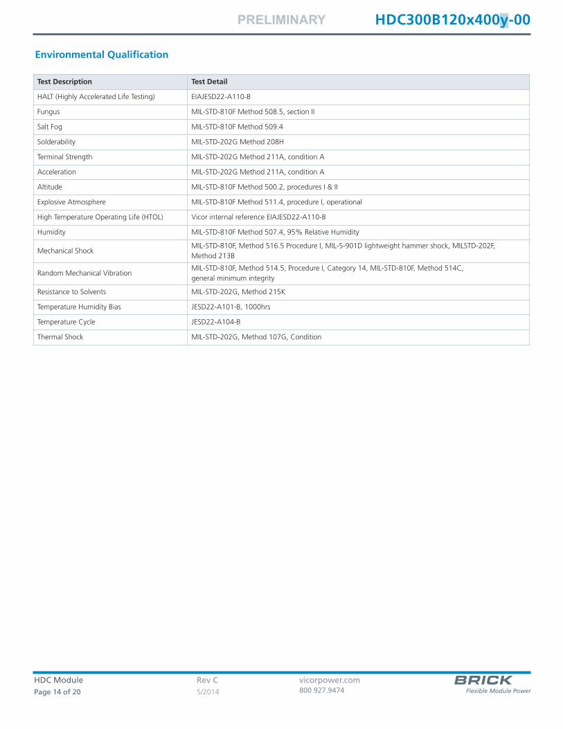
Test Description Test Detail
HALT (Highly Accelerated Life Testing) EIAJESD22-A110-B
Fungus MIL-STD-810F Method 508.5, section II
Salt Fog MIL-STD-810F Method 509.4
Solderability MIL-STD-202G Method 208H
Terminal Strength MIL-STD-202G Method 211A, condition A
Acceleration MIL-STD-202G Method 211A, condition A
Altitude MIL-STD-810F Method 500.2, procedures I & II
Explosive Atmosphere MIL-STD-810F Method 511.4, procedure I, operational
High Temperature Operating Life (HTOL) Vicor internal reference EIAJESD22-A110-B
Humidity MIL-STD-810F Method 507.4, 95% Relative Humidity
Mechanical ShockMIL-STD-810F, Method 516.5 Procedure I, MIL-S-901D lightweight hammer shock, MILSTD-202F,Method 213B
Random Mechanical VibrationMIL-STD-810F, Method 514.5, Procedure I, Category 14, MIL-STD-810F, Method 514C,general minimum integrity
Resistance to Solvents MIL-STD-202G, Method 215K
Temperature Humidity Bias JESD22-A101-B, 1000hrs
Temperature Cycle JESD22-A104-B
Thermal Shock MIL-STD-202G, Method 107G, Condition
Environmental Qualification

PRELIMINARY
HDC Module Rev C vicorpower.comPage 15 of 20 5/2014 800 927.9474
HDC 300 B 120 x 400 y-00
Pin Functions
+IN, -INInput power pins. -IN is the reference for all control pins, andtherefore a Kelvin connection is recommended to reduce effects ofvoltage drop due to -IN currents.
+OUT, -OUTOutput power pins.
PC (Primary Control)This pin enables and disables the converter; when held low the unitwill be disabled. It is referenced to the -IN pin of the converter. ThePC pin has an internal pull-up to VDD_INT through a 10 kΩ resistor.
n Output enable: When PC is allowed to float above the enablethreshold, the module is enabled. If leave PC floating, it is pulledup to VDD and module will be enabled.
n Output disable: PC may be pulled down externally in order todisable the module.
FT (Fault)The FT pin provides a Fault signal. Anytime the module is enabledand has not recognized a fault, the FT pin is inactive. Whenever thepowertrain stops (due to a fault protection or disabling the moduleby pulling PC low), the FT pin becomes active and provides currentto drive an external circuit. The FT pin becomes active momentarilywhen the module starts up.
When active, FT pin drives to VDD, with up to 5 mA of externalloading. Module may be damaged from an over-current FT drive,thus a resistor in series for current limiting is recommended.
Remote Sense (+S, -S)The Remote Sense pins sense the voltage at the load and adjusts theconverter output voltage to compensate for the voltage drop in theleads/traces. The sense leads of the module must always terminateeither directly to the output pins (local sense) or at the load(remote sense).
VDD3.3 V regulated voltage for external ancillary circuits.
VDDBSemi-regulated voltage for future products.
TR (Trim)The TR pin is used to select the trim mode and to trim the outputvoltage of the converter. The TR pin has an internal pull-up to VDD_INT
through a 5.11 kΩ resistor.
The converter shall latch trim behavior at application of VIN, andpersist in that same behavior until loss of input voltage.
n At application of VIN, if TR is sampled at above VTRIM-DIS, themodule shall latch in a non-trim mode, and will ignore the TR inputfor as long as VIN is present.
n At application of VIN, if TR is sampled at below VTRIM-EN, the TRwill serve as an input to control real time output voltage trim. It willpersist in this behavior until VIN is no longer present.
If trim is active, the TR pin provides dynamic trim control at a typical500 Hz of -3dB bandwidth over the output voltage. VOUT set pointunder full load and room temperature can be calculated using theequation below:
FB (Feedback)The FB pin produces PWM pulses whose duty cycle is maintained bythe internal Digital Supervisor to regulate the output voltage. Thispin will be used for paralleling modules to create high current/powerarrays in the future.
SGND
Signal ground for referencing all control circuitry.
Soft Start
The first time the HDC starts after application of input voltage, it willgo through a soft start sequence. Notice that the module will onlystartup if input voltage is inside the range of VIN-FULL-POWER. Afterstartup, the module can then operate in the entire VIN range.
This soft start sequence permits initial startup into a completelydischarged load capacitance. The soft start sequence ramps theoutput voltage by modulating the internal error amplifier reference.
VOUT = 1 + 0.171 • - 0.425 • VOUT_NOM 3.3 • Rtrim
5110 + Rtrim( )[ ]
3.3V
5.11k
Rtrim
TR
Rtrim = 1,277,500 • (-40 VOUT + 23 VOUT_NOM )
10,000 VOUT - 11,393 VOUT_NOM

PRELIMINARY
HDC Module Rev C vicorpower.comPage 16 of 20 5/2014 800 927.9474
HDC 300 B 120 x 400 y-00
This causes the output voltage to approximate a piecewise linearramp. The output ramp finishes then the voltage reaches either thenominal output voltage or the trimmed output voltage in caseswhere trim mode is active.
An HDC recovering from any fault condition does not assume thatthe output capacitance has remained charged. Just as with its initialstartup sequence when VIN is first applied, it will again execute thesoft start ramp.
Output Current Limit
The HDC features a fully operational current limit whicheffectively keeps the module operating inside the Safe OperatingArea (SOA) for all valid trim and load profiles. The current limitapproximates a “brick wall” limit, where the output current isprevented from exceeding the current limit threshold by reducingthe output voltage via the internal error amplifier reference. OutputOverload protection threshold is typically 105% of maximum outputcurrent, and can vary from 100% to 120% of maximumoutput current.
When the output current exceeds the current limit threshold, currentlimit action is postponed by 1ms, which permits the converter tomomentarily deliver higher peak output currents to the load. Peakoutput power during this time is still constrained by the internalPower Limit of the module. The fast Power Limit and relatively slowCurrent Limit work together to keep the module inside the SOA.Delaying entry into current limit also permits the converter tominimize droop voltage for load steps. Sustained operation incurrent limit is permitted, and no derating of output power isrequired in an array. Some applications may benefit from wellmatched current distribution, in which case fine tuning sharing viathe trim pins permits control over sharing. The converter does notrequire this for proper operation, due to the power limit and currentlimit behaviors described here. Current limit can reduce the outputvoltage to as little as the UVP threshold (VOUT-UVP). Below thisminimum output voltage compliance level, further loading willcause the module to shut down due to the output undervoltagefault protection.
Line Impedance and Output Stability Requirements
Connect a high-quality, low-noise power supply to the +IN and –INterminals. The interconnect cables can be up to 1 meter long eachway, and up to 0.1 m apart between each other. Additionalcapacitance may have to be added between +IN and –IN to make upfor impedances in the interconnect cables as well as deficiencies inthe source. Significant source impedance can bring system stabilityissue for a regulated DC-DC converter and needs to be avoidedor compensated.
Make sure input voltage slew rate dVin/dt is less than 1 V/us,otherwise a pre-charge circuit is required in the input side to controlthe charging slew rate. For the HDC, the output voltage stability isguaranteed as long as hold up capacitance COUT falls within thespecified ranges.
Input Fuse Selection
The HDC is not internally fused, see safety approvals for requiredfusing.
Fault Handling
Input Undervoltage Fault Protection (UVLO)
The converter’s input voltage is monitored to detect an input undervoltage condition. If the converter is not already running, then it willignore enable commands until the input voltage is greater thanVIN-UVLO+. If the converter is running and the input voltage fallsbelow VIN-UVLO-, the converter recognizes a fault condition, thepowertrain stops switching, and the output voltage of the unit falls.
UVLO faults which are shorter than tUVLO may not be detected by thefault sequence logic, in which case the converter may not respond.After a UVLO fault is detected by the fault sequence logic and theconverter shuts down as a result, it will wait for the input voltage torise above VIN-UVLO+. Provided the converter is still enabled, thepowertrain will again enter the soft start sequence.
Input Overvoltage Fault Protection (OVLO)
The converter’s input voltage is monitored to detect an input overvoltage condition. When the input voltage is more than the VIN-OVLO-,a fault is detected, the powertrain immediately stops switching, andthe output voltage of the converter falls.
After an OVLO fault occurs, the converter will wait for the inputvoltage to fall below VIN-OVLO-. Provided the converter is still enabled,the powertrain will again enter the soft start sequence.
The powertrain controller itself also monitors the input voltage.Transient OVLO events which have not yet been detected by the faultsequence logic may first be detected by the controller, if the inputslew rate is sufficiently large. In this case, powertrain switching willimmediately stop. If the input voltage falls back in range before thefault sequence logic detects the out of range condition, thepowertrain will resume switching and the fault logic will notinterrupt operation Regardless of whether the powertrain is runningat the time or not, if the input voltage does not recover from OVLObefore tOVLO, the converter fault logic will detect the fault.
Output Undervoltage Fault Protection (UVP)
The converter determines that an output overload or short circuitcondition exists by measuring its primary sensed output voltage. Ingeneral, whenever the powertrain is switching and the primary-sensed output voltage falls below VOUT-UVP threshold, a short circuitfault will be registered. Once an output undervoltage condition isdetected, the powertrain immediately stops switching, and theoutput voltage of the converter falls. The converter remains disabledfor a time tFAULT and then provided the converter is still enabled, thepowertrain will again enter the soft start sequence aftertINIT and tON.
Temperature Fault Protections (OTP)
The fault logic monitors the internal temperature of the converter. Ifthe measured temperature goes higher than TINT-OTP, a temperaturefault is registered. As with the undervoltage fault protection, once atemperature fault is registered, the powertrain immediately stopsswitching, the output voltage of the converter falls, and the converterremains disabled for a time tFAULT. Then, the converter waits for theinternal temperature to return to below TINT-OTP before recovering.Once recovered, provided the converter is still enabled, the HDC willagain enter the soft start sequence after tINIT and tON.

PRELIMINARY
HDC Module Rev C vicorpower.comPage 17 of 20 5/2014 800 927.9474
HDC 300 B 120 x 400 y-00
Output Overvoltage Fault Protection (OVP)
The converter monitors the primary sensed output voltage duringswitching to detect output OVP. If the primary sensed output voltageexceeds VOUT-OVP, a fault is latched, the logic disables the powertrain,and the output voltage of the converter falls.
This type of fault is latched, and the converter will not operateuntil the latch is cleared. Clearing the fault latch is achieved by eitherdisabling the converter via the PC pin, or else by removing theinput power.
Burst Mode
Under light loading conditions, the HD Converter may operate inburst mode depending on the line voltage. Burst mode occurswhenever the internal power consumption of the convertercombined with the external output load is less than the minimumpower transfer per switching cycle. To prevent the output voltagefrom rising in this case, the powertrain is switched off and onrepeatedly to effectively lower the average switching frequency, andpermit operation with no external load. During the time when thepower train is off, the module internal consumption is significantlyreduced, and there is a notable reduction in no-load input power inburst mode.
Pin Solderability
Please refer to the Soldering Methods and Procedures for VicorPower Modules application note for guidance on soldering the HDCmodule to printed circuit boards. The application note can be foundat: www.vicorpower.com/documents/application_notes/an_powermodulesoldering.pdf
PRELIMINARY
HDC Module Rev C vicorpower.comPage 18 of 20 5/2014 800 927.9474
HDC 300 B 120 x 400 y-00
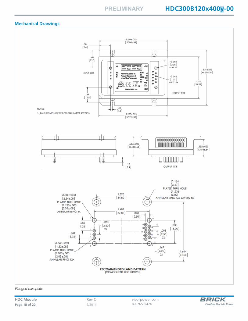
Mechanical Drawings
Flanged baseplate

PRELIMINARY
HDC Module Rev C vicorpower.comPage 19 of 20 5/2014 800 927.9474
HDC 300 B 120 x 400 y-00
Mechanical Drawings (Cont.)
.153.9
1.377±.01534.99±.38
.379.5
.3910.0
2.275±.01557.79±.38
.0822.08
MAX 4X
.0421.07
MAX 12X
OUTPUT SIDE
1.48837.80
.63016.00
.0982.507X
.0982.50
.1674.252X
.2857.25
.1483.75
.0982.502X
.060±.0031.52±.08
PLATED THRU HOLE.080 .003
[2.03 .08] ANNULAR RING 12X
.100±.0032.54±.08
PLATED THRU HOLE.120 .003
[3.05 .08 ] ANNULAR RING 4X
6
16
8
10
12
14
13
11
7
9
5
43
2
1
RECOMMENDED LAND PATTERN(COMPONENT SIDE SHOWN)
15
.630±.02516.00±.64
OUTPUT SIDE
INPUT SIDE
Flangeless baseplate

PRELIMINARY
HDC Module Rev C vicorpower.comPage 20 of 20 5/2014 800 927.9474
HDC 300 B 120 x 400 y-00
Vicor’s comprehensive line of power solutions includes high density AC-DC and DC-DC modules andaccessory components, fully configurable AC-DC and DC-DC power supplies, and complete custompower systems.
Information furnished by Vicor is believed to be accurate and reliable. However, no responsibility is assumed by Vicor for its use. Vicor makes norepresentations or warranties with respect to the accuracy or completeness of the contents of this publication. Vicor reserves the right to makechanges to any products, specifications, and product descriptions at any time without notice. Information published by Vicor has been checked andis believed to be accurate at the time it was printed; however, Vicor assumes no responsibility for inaccuracies. Testing and other quality controls areused to the extent Vicor deems necessary to support Vicor’s product warranty. Except where mandated by government requirements, testing of allparameters of each product is not necessarily performed. Specifications are subject to change without notice.
Vicor’s Standard Terms and ConditionsAll sales are subject to Vicor’s Standard Terms and Conditions of Sale, which are available on Vicor’s webpage or upon request.
Product WarrantyIn Vicor’s standard terms and conditions of sale, Vicor warrants that its products are free from non-conformity to its Standard Specifications (the“Express Limited Warranty”). This warranty is extended only to the original Buyer for the period expiring two (2) years after the date of shipmentand is not transferable.UNLESS OTHERWISE EXPRESSLY STATED IN A WRITTEN SALES AGREEMENT SIGNED BY A DULY AUTHORIZED VICOR SIGNATORY, VICOR DISCLAIMSALL REPRESENTATIONS, LIABILITIES, AND WARRANTIES OF ANY KIND (WHETHER ARISING BY IMPLICATION OR BY OPERATION OF LAW) WITHRESPECT TO THE PRODUCTS, INCLUDING, WITHOUT LIMITATION, ANY WARRANTIES OR REPRESENTATIONS AS TO MERCHANTABILITY, FITNESS FORPARTICULAR PURPOSE, INFRINGEMENT OF ANY PATENT, COPYRIGHT, OR OTHER INTELLECTUAL PROPERTY RIGHT, OR ANY OTHER MATTER.
This warranty does not extend to products subjected to misuse, accident, or improper application, maintenance, or storage. Vicor shall not be liablefor collateral or consequential damage. Vicor disclaims any and all liability arising out of the application or use of any product or circuit and assumesno liability for applications assistance or buyer product design. Buyers are responsible for their products and applications using Vicor products andcomponents. Prior to using or distributing any products that include Vicor components, buyers should provide adequate design, testing andoperating safeguards.
Vicor will repair or replace defective products in accordance with its own best judgment. For service under this warranty, the buyer must contactVicor to obtain a Return Material Authorization (RMA) number and shipping instructions. Products returned without prior authorization will bereturned to the buyer. The buyer will pay all charges incurred in returning the product to the factory. Vicor will pay all reshipment charges if theproduct was defective within the terms of this warranty.
Life Support PolicyVICOR’S PRODUCTS ARE NOT AUTHORIZED FOR USE AS CRITICAL COMPONENTS IN LIFE SUPPORT DEVICES OR SYSTEMS WITHOUT THE EXPRESSPRIOR WRITTEN APPROVAL OF THE CHIEF EXECUTIVE OFFICER AND GENERAL COUNSEL OF VICOR CORPORATION. As used herein, life supportdevices or systems are devices which (a) are intended for surgical implant into the body, or (b) support or sustain life and whose failure to performwhen properly used in accordance with instructions for use provided in the labeling can be reasonably expected to result in a significant injury to theuser. A critical component is any component in a life support device or system whose failure to perform can be reasonably expected to cause thefailure of the life support device or system or to affect its safety or effectiveness. Per Vicor Terms and Conditions of Sale, the user of Vicor productsand components in life support applications assumes all risks of such use and indemnifies Vicor against all liability and damages.
Intellectual Property NoticeVicor and its subsidiaries own Intellectual Property (including issued U.S. and Foreign Patents and pending patent applications) relating to theproducts described in this data sheet. No license, whether express, implied, or arising by estoppel or otherwise, to any intellectual property rights isgranted by this document. Interested parties should contact Vicor's Intellectual Property Department.
The products described on this data sheet are protected by the following U.S. Patents Numbers:RE40,072; 7,561,446; 7,920,391; 7,782,639; 8,427,269; 6,421,262 and other patents pending.
Vicor Corporation25 Frontage Road
Andover, MA, USA 01810Tel: 800-735-6200Fax: 978-475-6715
emailCustomer Service: [email protected]
Technical Support: [email protected]