iso1050 isolated can transceiver (rev. i)
TRANSCRIPT
RXD
TXD
CANH
CANL
Iso
lati
on
Ca
pa
cito
r
Product
Folder
Order
Now
Technical
Documents
Tools &
Software
Support &Community
An IMPORTANT NOTICE at the end of this data sheet addresses availability, warranty, changes, use in safety-critical applications,intellectual property matters and other important disclaimers. PRODUCTION DATA.
ISO1050SLLS983I –JUNE 2009–REVISED JANUARY 2015
ISO1050 Isolated CAN Transceiver
1
1 Features1• Meets the Requirements of ISO11898-2• 5000-VRMS Isolation (ISO1050DW)• 2500-VRMS Isolation (ISO1050DUB)• Fail-Safe Outputs• Low Loop Delay: 150 ns (Typical), 210 ns
(Maximum)• 50-kV/μs Typical Transient Immunity• Bus-Fault Protection of –27 V to 40 V• Driver (TXD) Dominant Time-out Function• I/O Voltage Range Supports 3.3-V and 5-V
Microprocessors• VDE Approval per DIN V VDE V 0884-10 (VDE V
0884-10):2006-12 and DIN EN 61010-1• UL 1577 Approved• CSA Approved for IEC 60950-1, IEC 61010-1,
IEC 60601-1 3rd Ed (Medical) and ComponentAcceptance Notice 5A
• TUV 5-KVRMS Reinforced Insulation Approval forEN/UL/CSA 60950-1 (ISO1050DW-Only)
• CQC Reinforced Insulation per GB4843.1-2011(ISO1050DW-Only)
• Typical 25-Year Life at Rated Working Voltage(see Application Report SLLA197 and LifeExpectancy vs Working Voltage)
2 Applications• Industrial Automation, Control, Sensors, and Drive
Systems• Building and Climate Control (HVAC) Automation• Security Systems• Transportation• Medical• Telecom• CAN Bus Standards Such as CANopen,
DeviceNet, NMEA2000, ARINC825, ISO11783,CAN Kingdom, CANaerospace
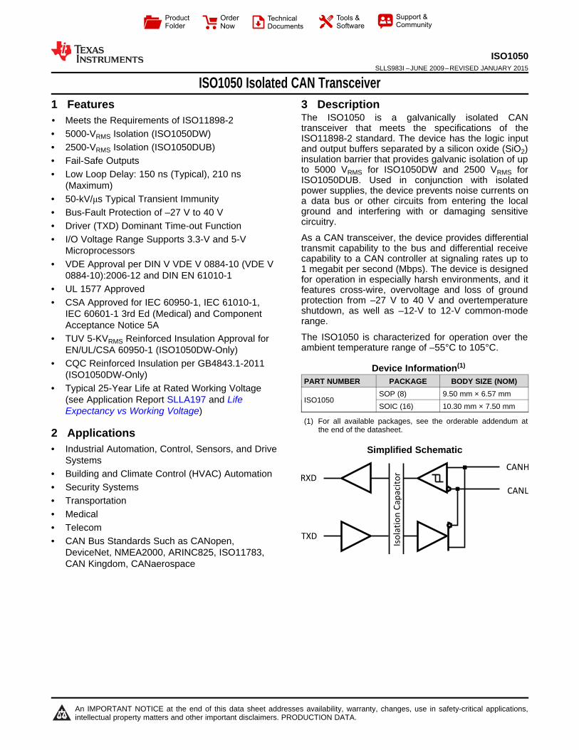
3 DescriptionThe ISO1050 is a galvanically isolated CANtransceiver that meets the specifications of theISO11898-2 standard. The device has the logic inputand output buffers separated by a silicon oxide (SiO2)insulation barrier that provides galvanic isolation of upto 5000 VRMS for ISO1050DW and 2500 VRMS forISO1050DUB. Used in conjunction with isolatedpower supplies, the device prevents noise currents ona data bus or other circuits from entering the localground and interfering with or damaging sensitivecircuitry.
As a CAN transceiver, the device provides differentialtransmit capability to the bus and differential receivecapability to a CAN controller at signaling rates up to1 megabit per second (Mbps). The device is designedfor operation in especially harsh environments, and itfeatures cross-wire, overvoltage and loss of groundprotection from –27 V to 40 V and overtemperatureshutdown, as well as –12-V to 12-V common-moderange.
The ISO1050 is characterized for operation over theambient temperature range of –55°C to 105°C.
Device Information(1)
PART NUMBER PACKAGE BODY SIZE (NOM)
ISO1050SOP (8) 9.50 mm × 6.57 mmSOIC (16) 10.30 mm × 7.50 mm
(1) For all available packages, see the orderable addendum atthe end of the datasheet.
Simplified Schematic
2
ISO1050SLLS983I –JUNE 2009–REVISED JANUARY 2015 www.ti.com
Product Folder Links: ISO1050
Submit Documentation Feedback Copyright © 2009–2015, Texas Instruments Incorporated
Table of Contents1 Features .................................................................. 12 Applications ........................................................... 13 Description ............................................................. 14 Revision History..................................................... 25 Pin Configuration and Functions ......................... 56 Specifications......................................................... 6
6.1 Absolute Maximum Ratings ..................................... 66.2 ESD Ratings.............................................................. 66.3 Recommended Operating Conditions....................... 66.4 Thermal Information .................................................. 76.5 Electrical Characteristics: Supply Current................. 76.6 Electrical Characteristics: Driver ............................... 76.7 Electrical Characteristics: Receiver .......................... 86.8 Switching Characteristics: Device............................. 86.9 Switching Characteristics: Driver .............................. 86.10 Switching Characteristics: Receiver........................ 96.11 Typical Characteristics ............................................ 9
7 Parameter Measurement Information ................ 10
8 Detailed Description ............................................ 158.1 Overview ................................................................. 158.2 Functional Block Diagram ....................................... 158.3 Feature Description................................................. 158.4 Device Functional Modes........................................ 20
9 Application and Implementation ........................ 229.1 Application Information............................................ 229.2 Typical Application .................................................. 22
10 Power Supply Recommendations ..................... 2511 Layout................................................................... 25
11.1 Layout Guidelines ................................................. 2511.2 Layout Example .................................................... 25
12 Device and Documentation Support ................. 2612.1 Documentation Support ........................................ 2612.2 Trademarks ........................................................... 2612.3 Electrostatic Discharge Caution............................ 2612.4 Glossary ................................................................ 26
13 Mechanical, Packaging, and OrderableInformation ........................................................... 26
4 Revision HistoryNOTE: Page numbers for previous revisions may differ from page numbers in the current version.
Changes from Revision H (June 2013) to Revision I Page
• Added Pin Configuration and Functions section, ESD Ratings table, Feature Description section, Device FunctionalModes, Application and Implementation section, Power Supply Recommendations section, Layout section, Deviceand Documentation Support section, and Mechanical, Packaging, and Orderable Information section .............................. 1
Changes from Revision G (March 2013) to Revision H Page
• Changed title From: LIFE EXPECTANCY vs WORKING VOLTAGE (ISO1050DW To: LIFE EXPECTANCY vsWORKING VOLTAGE (ISO1050DUB)................................................................................................................................. 21
Changes from Revision F (January 2013) to Revision G Page
• Clarified clearance and creepage measurement method in ISOLATOR CHARACTERISTICS .......................................... 15• Clarified test methods for voltage ratings in INSULATION CHARACTERISTICS ............................................................... 16• Changed UL Single Protection Certification pending to Single Protection in REGULATORY INFORMATION
SECTION (certificate available)............................................................................................................................................ 17
Changes from Revision E (December 2011) to Revision F Page
• Deleted ISO1050L device....................................................................................................................................................... 1• Deleted ISO1050LDW from Features list ............................................................................................................................... 1• Deleted ISO1050LDW in first paragraph of DESCRIPTION .................................................................................................. 1• Added the PIN FUNCTIONS section...................................................................................................................................... 5• Added Note 1 to the DRIVER SWITCHING CHARACTERISTICS table ............................................................................... 8• Deleted ISO1050LDW from INSULATION CHARACTERISTICS ........................................................................................ 16• Deleted ISO1050LDW from REGULATORY INFORMATION.............................................................................................. 17• Added the FUNCTIONAL DESCRIPTION section ............................................................................................................... 17
3
ISO1050www.ti.com SLLS983I –JUNE 2009–REVISED JANUARY 2015
Product Folder Links: ISO1050
Submit Documentation FeedbackCopyright © 2009–2015, Texas Instruments Incorporated
• Deleted ISO1050LDW from LIFE EXPECTANCY vs WORKING VOLTAGE ..................................................................... 21• Deleted 40V from the CANH and CANL input diagrams and output diagrams in the EQUIVALENT I/O
SCHEMATICS ..................................................................................................................................................................... 21• Changed the APPLICATION INFORMATION section.......................................................................................................... 22• Changed the BUS LOADING, LENGHT AND NUMBER OF NODES section ..................................................................... 22• Added the CAN TERMINATION section .............................................................................................................................. 23
Changes from Revision D (June 2011) to Revision E Page
• Added device ISO1050L......................................................................................................................................................... 1• Changed (DW Package) in the Features list to (ISO1050DW) .............................................................................................. 1• Changed (DUB Package) in the Features list to (ISO1050DUB and ISO1050LDW)............................................................. 1• Deleted IEC 60950-1 from the CSA Approvals Feature bullet ............................................................................................... 1• From: IEC 60601-1 (Medical) and CSA Approvals Pending To: IEC 60601-1 (Medical) and CSA Approved ...................... 1• Added Feature - 5 KVRMS Reinforced.. ................................................................................................................................ 1• Changed DW Package to ISO105DW and DUB package to ISO1050DUB and ISO1050LDW in the first paragraph
of DESCRIPTION ................................................................................................................................................................... 1• Added Note 1 to the INSULATION CHARACTERISTICS table........................................................................................... 16• Changed VIORM From: 8-DUB Package to ISO1050DUB and ISO1050LDW ...................................................................... 16• Changed VIORM From: 16-DW to ISO1050DW .................................................................................................................... 16• Changed the VISO Isolation voltage per UL section of the INSULATION CHARACTERISTICS table. ................................ 16• Changed the IEC 60664-1 Ratings Table ............................................................................................................................ 16• Changed the REGULATORY INFORMATION table ............................................................................................................ 17• Changed in note (1) 3000 to 2500 and 6000 to 5000 .......................................................................................................... 17• Changed From: File Number: 220991 (Approval Pending) To: File Number: 220991......................................................... 17• Changed in LIFE EXPECTANCY vs WORKING VOLTAGE (8-DUB PACKAGE TO: LIFE.....(ISO1050DW and
ISO1050LDW) ...................................................................................................................................................................... 21
Changes from Revision C (July 2010) to Revision D Page
• Changed the SUPPLY CURRENT table for ICC1 1st row From: Typ = 1 To: 1.8 and MAX = 2 To: 2.8................................. 7• Changed the SUPPLY CURRENT table for ICC1 2nd row From: Typ = 2 To: 2.8 and MAX = 3 To: 3.6 ............................... 7• Changed the REGULATORY INFORMATION table ............................................................................................................ 17
Changes from Revision B (June 2009) to Revision C Page
• Changed the IEC 60747-5-2 Features bullet From: DW package Approval Pending To: VDE approved for both DUBand DW packages .................................................................................................................................................................. 1
• Changed the Minimum Internal Gap value from 0.008 to 0.014 in the Isolator Characteristics table.................................. 15• Changed VIORM Specification From: 1300 To: 1200 per VDE certification ........................................................................... 16• Changed VPR Specification From 2438 To: 2250 ................................................................................................................. 16• Added the Bus Loading paragraph to the Application Information section .......................................................................... 22

4
ISO1050SLLS983I –JUNE 2009–REVISED JANUARY 2015 www.ti.com
Product Folder Links: ISO1050
Submit Documentation Feedback Copyright © 2009–2015, Texas Instruments Incorporated
Changes from Revision A (Sept 2009) to Revision B Page
• Added information that IEC 60747-5-2 and IEC61010-1 have been approved...................................................................... 1• Changed DW package from preview to production data........................................................................................................ 5• Added Insulation Characteristics and IEC 60664-1 Ratings tables...................................................................................... 16• Added IEC file number ......................................................................................................................................................... 17
Changes from Original (June 2009) to Revision A Page
• Added Typical 25-Year Life at Rated Working Voltage to Features....................................................................................... 1• Added LIFE EXPECTANCY vs WORKING VOLTAGE section ........................................................................................... 21

5
ISO1050www.ti.com SLLS983I –JUNE 2009–REVISED JANUARY 2015
Product Folder Links: ISO1050
Submit Documentation FeedbackCopyright © 2009–2015, Texas Instruments Incorporated
5 Pin Configuration and Functions
16-PinDW Package
Top View
8-PinDUB Package
Top View
Pin FunctionsPIN
TYPE DESCRIPTIONNAME DW DUB
VCC1 1 1 Supply Digital-side supply voltage (3 to 5.5 V)
GND1 2 — Ground Digital-side ground connection
RXD 3 2 O CAN receive data output (LOW for dominant and HIGH for recessive bus states)
NC 4 — NC No connect
NC 5 — NC No connect
TXD 6 3 I CAN transmit data input (LOW for dominant and HIGH for recessive bus states)
GND1 7 4 Ground Digital-side ground connection
GND1 8 — Ground Digital-side ground connection
GND2 9 5 Ground Transceiver-side ground connection
GND2 10 — Ground Transceiver-side ground connection
NC 11 — NC No connect
CANL 12 6 I/O Low-level CAN bus line
CANH 13 7 I/O High-level CAN bus line
NC 14 — NC No connect
GND2 15 — Ground Transceiver-side ground connection
VCC2 16 8 Supply Transceiver-side supply voltage (5 V)
6
ISO1050SLLS983I –JUNE 2009–REVISED JANUARY 2015 www.ti.com
Product Folder Links: ISO1050
Submit Documentation Feedback Copyright © 2009–2015, Texas Instruments Incorporated
(1) Stresses beyond those listed under Absolute Maximum Ratings may cause permanent damage to the device. These are stress ratingsonly and functional operation of the device at these or any other conditions beyond those indicated under Recommended OperatingConditions is not implied. Exposure to absolute-maximum-rated conditions for extended periods may affect device reliability.
(2) This isolator is suitable for isolation within the safety limiting data. Maintenance of the safety data must be ensured by means ofprotective circuitry.
(3) All input and output logic voltage values are measured with respect to the GND1 logic side ground. Differential bus-side voltages aremeasured to the respective bus-side GND2 ground terminal.
(4) Maximum voltage must not exceed 6 V.
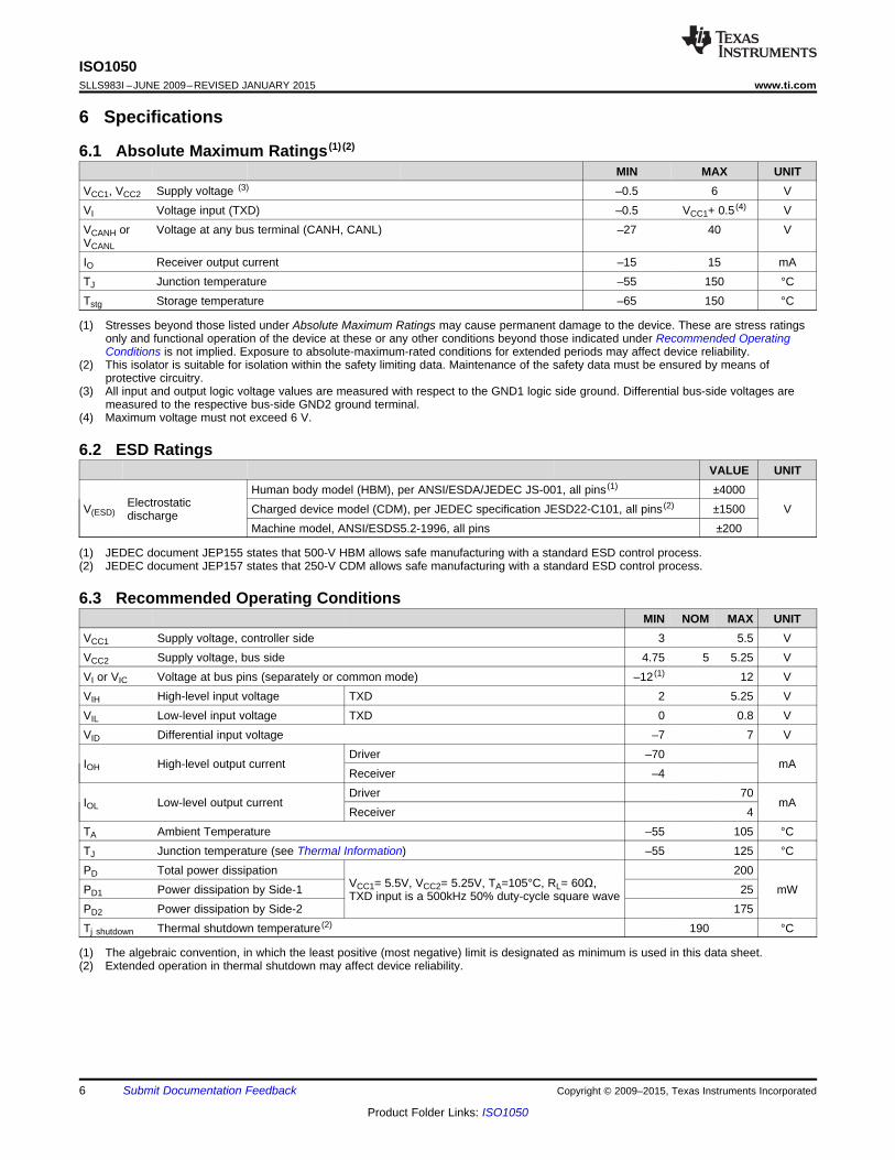
6 Specifications
6.1 Absolute Maximum Ratings (1) (2)
MIN MAX UNITVCC1, VCC2 Supply voltage (3) –0.5 6 VVI Voltage input (TXD) –0.5 VCC1+ 0.5 (4) VVCANH orVCANL
Voltage at any bus terminal (CANH, CANL) –27 40 V
IO Receiver output current –15 15 mATJ Junction temperature –55 150 °CTstg Storage temperature –65 150 °C
(1) JEDEC document JEP155 states that 500-V HBM allows safe manufacturing with a standard ESD control process.(2) JEDEC document JEP157 states that 250-V CDM allows safe manufacturing with a standard ESD control process.
6.2 ESD RatingsVALUE UNIT
V(ESD)Electrostaticdischarge
Human body model (HBM), per ANSI/ESDA/JEDEC JS-001, all pins (1) ±4000VCharged device model (CDM), per JEDEC specification JESD22-C101, all pins (2) ±1500
Machine model, ANSI/ESDS5.2-1996, all pins ±200
(1) The algebraic convention, in which the least positive (most negative) limit is designated as minimum is used in this data sheet.(2) Extended operation in thermal shutdown may affect device reliability.
6.3 Recommended Operating ConditionsMIN NOM MAX UNIT
VCC1 Supply voltage, controller side 3 5.5 VVCC2 Supply voltage, bus side 4.75 5 5.25 VVI or VIC Voltage at bus pins (separately or common mode) –12 (1) 12 VVIH High-level input voltage TXD 2 5.25 VVIL Low-level input voltage TXD 0 0.8 VVID Differential input voltage –7 7 V
IOH High-level output currentDriver –70
mAReceiver –4
IOL Low-level output currentDriver 70
mAReceiver 4
TA Ambient Temperature –55 105 °CTJ Junction temperature (see Thermal Information) –55 125 °CPD Total power dissipation
VCC1= 5.5V, VCC2= 5.25V, TA=105°C, RL= 60Ω,TXD input is a 500kHz 50% duty-cycle square wave
200mWPD1 Power dissipation by Side-1 25
PD2 Power dissipation by Side-2 175Tj shutdown Thermal shutdown temperature (2) 190 °C

7
ISO1050www.ti.com SLLS983I –JUNE 2009–REVISED JANUARY 2015
Product Folder Links: ISO1050
Submit Documentation FeedbackCopyright © 2009–2015, Texas Instruments Incorporated
(1) For more information about traditional and new thermal metrics, see the Semiconductor and IC Package Thermal Metrics applicationreport (SPRA953).
6.4 Thermal Information
THERMAL METRIC (1)ISO1050
UNITDW DUB16 PINS 8 PINS
RθJA Junction-to-ambient thermal resistance 76.0 73.3
°C/W
RθJC(top) Junction-to-case (top) thermal resistance 41 63.2RθJB Junction-to-board thermal resistance 47.7 43.0ψJT Junction-to-top characterization parameter 14.4 27.4ψJB Junction-to-board characterization parameter 38.2 42.7RθJC(bot) Junction-to-case (bottom) thermal resistance n/a n/a
(1) All typical values are at 25°C with VCC1 = VCC2 = 5 V.
6.5 Electrical Characteristics: Supply Currentover recommended operating conditions (unless otherwise noted)
PARAMETER TEST CONDITIONS MIN TYP (1) MAX UNIT
ICC1 VCC1 Supply currentVI = 0 V or VCC1 , VCC1 = 3.3V 1.8 2.8
mAVI = 0 V or VCC1 , VCC1 = 5V 2.3 3.6
ICC2 VCC2 Supply currentDominant VI = 0 V, 60-Ω Load 52 73
mARecessive VI = VCC1 8 12
6.6 Electrical Characteristics: Driverover recommended operating conditions (unless otherwise noted)
PARAMETER TEST CONDITIONS MIN TYP MAX UNIT
VO(D) Bus output voltage (Dominant)CANH
See Figure 7 and Figure 8, VI = 0 V, RL = 60 Ω2.9 3.5 4.5
VCANL 0.8 1.2 1.5
VO(R) Bus output voltage (Recessive) See Figure 7 and Figure 8, VI = 2 V, RL= 60 Ω 2 2.3 3 V
VOD(D) Differential output voltage (Dominant)
See Figure 7, Figure 8 and Figure 9, VI = 0 V,RL = 60 Ω 1.5 3
VSee Figure 7, Figure 8, and Figure 9 VI = 0 V,RL = 45Ω, Vcc > 4.8 V 1.4 3
VOD(R) Differential output voltage (Recessive)See Figure 7 and Figure 8, VI = 3 V, RL = 60 Ω –0.12 0.012
VVI = 3 V, No Load –0.5 0.05
VOC(D) Common-mode output voltage (Dominant)See Figure 14
2 2.3 3V
VOC(pp) Peak-to-peak common-mode output voltage 0.3IIH High-level input current, TXD input VI at 2 V 5 μAIIL Low-level input current, TXD input VI at 0.8 V –5 μAIO(off) Power-off TXD leakage current VCC1, VCC2 at 0 V, TXD at 5 V 10 μA
IOS(ss) Short-circuit steady-state output current
See Figure 17, VCANH = –12 V, CANL Open –105 –72
mASee Figure 17, VCANH = 12 V, CANL Open 0.36 1See Figure 17, VCANL =–12 V, CANH Open –1 –0.5See Figure 17, VCANL = 12 V, CANH Open 71 105
CO Output capacitance See receiver input capacitanceCMTI Common-mode transient immunity See Figure 19, VI = VCC or 0 V 25 50 kV/μs

8
ISO1050SLLS983I –JUNE 2009–REVISED JANUARY 2015 www.ti.com
Product Folder Links: ISO1050
Submit Documentation Feedback Copyright © 2009–2015, Texas Instruments Incorporated
(1) All typical values are at 25°C with VCC1 = VCC2 = 5 V.
6.7 Electrical Characteristics: Receiverover recommended operating conditions (unless otherwise noted)
PARAMETER TEST CONDITIONS MIN TYP (1) MAX UNITVIT+ Positive-going bus input threshold voltage
See Table 1750 900 mV
VIT– Negative-going bus input threshold voltage 500 650 mVVhys Hysteresis voltage (VIT+ – VIT–) 150 mV
VOH High-level output voltage with Vcc = 5 VIOH = –4 mA, See Figure 12 VCC – 0.8 4.6
VIOH = –20 μA, See Figure 12 VCC – 0.1 5
VOH High-level output voltage with Vcc1 = 3.3 VIOL = 4 mA, See Figure 12 VCC – 0.8 3.1
VIOL = 20 μA, See Figure 12 VCC – 0.1 3.3
VOL Low-level output voltageIOL = 4 mA, See Figure 12 0.2 0.4
VIOL = 20 μA, See Figure 12 0 0.1
CI Input capacitance to ground, (CANH or CANL) TXD at 3 V, VI = 0.4 sin (4E6πt) + 2.5 V 6 pFCID Differential input capacitance TXD at 3 V, VI = 0.4 sin (4E6πt) 3 pFRID Differential input resistance TXD at 3 V 30 80 kΩRIN Input resistance (CANH or CANL) TXD at 3 V 15 30 40 kΩ
RI(m)Input resistance matching(1 – [RIN (CANH) / RIN (CANL)]) × 100% VCANH = VCANL –3% 0% 3%
CMTI Common-mode transient immunity VI = VCC or 0 V, See Figure 19 25 50 kV/μs
6.8 Switching Characteristics: Deviceover recommended operating conditions (unless otherwise noted)
PARAMETER TEST CONDITIONS MIN TYP MAX UNIT
tloop1Total loop delay, driver input to receiver output, Recessive toDominant See Figure 15 112 150 210 ns
tloop2Total loop delay, driver input to receiver output, Dominant toRecessive See Figure 15 112 150 210 ns
(1) The TXD dominant time out (tTXD_DTO) disables the driver of the transceiver once the TXD has been dominant longer than (tTXD_DTO)which releases the bus lines to recessive preventing a local failure from locking the bus dominant. The driver may only transmitdominant again after TXD has been returned HIGH (recessive). While this protects the bus from local faults locking the bus dominant itlimits the minimum data rate possible. The CAN protocol allows a maximum of eleven successive dominant bits (on TXD) for the worstcase where five successive dominant bits are followed immediately by an error frame. This along with the (tTXD_DTO) minimum limits theminimum bit rate. The minimum bit rate may be calculated by: Minimum Bit Rate = 11/ (tTXD_DTO) = 11 bits / 300 µs = 37 kbps.
6.9 Switching Characteristics: Driverover recommended operating conditions (unless otherwise noted)
PARAMETER TEST CONDITIONS MIN TYP MAX UNITtPLH Propagation delay time, recessive-to-dominant output
See Figure 10
31 74 110
nstPHL Propagation delay time, dominant-to-recessive output 25 44 75tr Differential output signal rise time 20 50tf Differential output signal fall time 20 50tTXD_DTO
(1) Dominant time-out ↓ CL=100 pF, See Figure 16 300 450 700 μs

1
10
100
250 350 450 550 650 750 850 950
Signaling Rate - kbps
I 1 = 3.3 VCC
I 1 = 5 VCC
I 2 = 5 VCC
I-
Su
pp
ly C
urr
en
t -
mA
CC
1
1.5
2
2.5
3
3.5
V = CANHO
-60 -40 -20 0 20 40 60 80 100 120
T - Free-Air Temperature - °CA
V-
Ou
tpu
t V
olt
ag
e -
VO
V = CANLO
140
150
160
170
180
190
200
-60 -40 -20 0 20 40 60 80 100 120
T - Free-Air Temperature - °CA
Lo
op
Tim
e -
ns
V 1 = 3 V,
V 2 = 4.75 VCC
CC
V 1 = 5 V,
V 2 = 5 VCC
CC
V 1 = 5.5 V,
V 2 = 5.25 VCC
CC
145
147
149
151
153
155
157
159
161
163
-60 -40 -20 0 20 40 60 80 100 120
T - Free-Air Temperature - °CA
Lo
op
Tim
e -
ns
V 1 = 3 V,
V 2 = 4.75 VCC
CC
V 1 = 5.5 V,
V 2 = 5.25 VCC
CC
V 1 = 5 V,
V 2 = 5 VCC
CC
9
ISO1050www.ti.com SLLS983I –JUNE 2009–REVISED JANUARY 2015
Product Folder Links: ISO1050
Submit Documentation FeedbackCopyright © 2009–2015, Texas Instruments Incorporated
6.10 Switching Characteristics: Receiverover recommended operating conditions (unless otherwise noted)
PARAMETER TEST CONDITIONS MIN TYP MAX UNITtPLH Propagation delay time, low-to-high-level output
TXD at 3 V, See Figure 12
66 90 130
nstPHL Propagation delay time, high-to-low-level output 51 80 105tr Output signal rise time 3 6tf Output signal fall time 3 6tfs Fail-Safe output delay time from bus-side power loss VCC1 at 5 V, See Figure 18 6 μs
6.11 Typical Characteristics
Figure 1. Recessive-to-Dominant Loop Time vs Free-AirTemperature (Across Vcc)
Figure 2. Dominant-to-Recessive Loop Time vs Free-AirTemperature (Across Vcc)
Figure 3. Supply Current (RMS) vs Signaling Rate (kbps) Figure 4. Driver Output Voltage vs Free-Air Temperature
Figure 5. Emissions Spectrum to 10 MHz Figure 6. Emissions Spectrum to 50 MHz

VI
(SEE NOTE A)
VO60TXD
CANL
CANH
±1%W CL = 100 pF
20%
(SEE NOTE B)
±
Vcc/2 Vcc/2
Vcc
tf
tr
tPLH
tPHL
10%
90%0.9V
0 V
VO(D)
VO(R)
0.5V
VI
VO
0 V VOD
-2V <Vtest< 7 V
330
60
330
TXD
CANL
CANH
±1%
±1%
±1%+_
W
W
W
GND2
» 2.5 V
» 3.5 V
» 1.5 V
Recessive
Dominant
O (CANH)V
O (CANL)V
0 or
Vcc1
VI
TXD
CANH
CANL
VO(CANL) VO(CANH)
VOD
IO(CANH)
IO(CANL)
GND2GND1
GND1 GND2
II
VOC
VO(CANH) + VO(CANL)
2
RL
10
ISO1050SLLS983I –JUNE 2009–REVISED JANUARY 2015 www.ti.com
Product Folder Links: ISO1050
Submit Documentation Feedback Copyright © 2009–2015, Texas Instruments Incorporated
7 Parameter Measurement Information
Figure 7. Driver Voltage, Current and Test Definitions
Figure 8. Bus Logic State Voltage Definitions
Figure 9. Driver VOD With Common-Mode Loading Test Circuit
A. The input pulse is supplied by a generator having the following characteristics: PRR ≤ 125 kHz, 50% duty cycle,tr ≤ 6 ns, tf ≤ 6 ns, ZO = 50 Ω.
B. CL includes instrumentation and fixture capacitance within ±20%.
Figure 10. Driver Test Circuit and Voltage Waveforms

RXD
CANH
CANL
GND 2 GND 1
V I
(SEE NOTE A) 1 .5 V
IO
V O
CL = 15 pF
20 %(SEE NOTE B)
±
VI
VO
2 V2.4 V
3.5 V
VOH
t ftr
t pHL
1.5 V
VOL
90 %
10 %0.3 Vcc 1
0.7 Vcc 1
tpLH
RXD
CANH
CANL
GND2 GND1
VI(CANH)
VI(CANL)
IO
VIC
VI(CANH)
=
VI(CANL)+2
VID
VO
11
ISO1050www.ti.com SLLS983I –JUNE 2009–REVISED JANUARY 2015
Product Folder Links: ISO1050
Submit Documentation FeedbackCopyright © 2009–2015, Texas Instruments Incorporated
Parameter Measurement Information (continued)
Figure 11. Receiver Voltage and Current Definitions
A. The input pulse is supplied by a generator having the following characteristics: PRR ≤ 125 kHz, 50% duty cycle,tr ≤ 6 ns, tf ≤ 6 ns, ZO = 50 Ω.
B. CL includes instrumentation and fixture capacitance within ±20%.
Figure 12. Receiver Test Circuit and Voltage Waveforms
Table 1. Differential Input Voltage Threshold TestINPUT OUTPUT
VCANH VCANL |VID| R–11.1 V –12 V 900 mV L
VOL12 V 11.1 V 900 mV L–6 V –12 V 6 V L12 V 6 V 6 V L
–11.5 V –12 V 500 mV H
VOH
12 V 11.5 V 500 mV H–12 V –6 V –6 V H6 V 12 V –6 V H
Open Open X H

TXD
RXD
60 WVI
15 pF
CANH
CANL
+
VO
_
±20%
±1%
GND1
TXD Input
0 V
Vcc
OutputRXD
50%
50%
VOH
VOL
tloop1
50%
tloop2
CANH
CANL47 nF
VI ± 20%
TXD
W27 ±1 %
W27 ±1 %OCV
=O(CANH)V
O(CANL)V+
2
GND1 GND 2
VOC
VOC(pp)
CANH
CANL
RXD
The waveforms of the applied transients are in accordance
with ISO 7637 part 1, test pulses 1, 2, 3a, and 3b.
TXD
1 nF
1 nF
15 pF
GND2 GND1
VI
+
_
12
ISO1050SLLS983I –JUNE 2009–REVISED JANUARY 2015 www.ti.com
Product Folder Links: ISO1050
Submit Documentation Feedback Copyright © 2009–2015, Texas Instruments Incorporated
Figure 13. Transient Overvoltage Test Circuit
Figure 14. Peak-to-Peak Output Voltage Test Circuit and Waveform
Figure 15. tLOOP Test Circuit and Voltage Waveforms

TXD
RXD
15pF
+
VO±20%
W60
CANH
CANL
±1%CL
NOTE:CL=100pF
includes instrumentationand fixture capacitancewithin ± 20%.
VCC 2
VI
0 V
GND 1
VOH
VCC2
0 Vtfs
VO
VI
2.7 V
VOL
50%
IOS
TXD
-12V or 12V
0 V or VCC1
CANH
CANL VI
GND2
IOS (P)IOS (SS)
15 s
VI
10 ms
0 V
0 V
12 V
-12 V
or
0 V
VI
RL= 60
(see Note B )
CANH
CANH
TXD±1%W
(see Note A )
CL
VI
VOD
GND 1
Vcc
VI
VOD 500 mV900 mV
0 V
VOD(D)
0 V
tTXD_DTO
13
ISO1050www.ti.com SLLS983I –JUNE 2009–REVISED JANUARY 2015
Product Folder Links: ISO1050
Submit Documentation FeedbackCopyright © 2009–2015, Texas Instruments Incorporated
A. The input pulse is supplied by a generator having the following characteristics: tr ≤ 6 ns, tf ≤ 6 ns, ZO = 50 Ω.B. CL includes instrumentation and fixture capacitance within ±20%.
Figure 16. Dominant Time-out Test Circuit and Voltage Waveforms
Figure 17. Driver Short-Circuit Current Test Circuit and Waveforms
Figure 18. Fail-Safe Delay Time Test Circuit and Voltage Waveforms

ISO1050
30 W
CANH
CANL
47nF 10 nF
Spectrum Analyzer
TXD500kbps
30 W
6.2 kW
6.2 kW
VOLVOH or
TXD
RXD
VCC 1
1 k W
60 W
VCC2
GND 1
V TEST
GND 2
CL = 15 pF
(includes probe and
jig capacitance)
C = 0.1 F 1%m ±CANH
CANL
GND1
C = 0.1 Fm
±1%
S 1
2.0 V
0.8 V
VOLVOH or
GND2
14
ISO1050SLLS983I –JUNE 2009–REVISED JANUARY 2015 www.ti.com
Product Folder Links: ISO1050
Submit Documentation Feedback Copyright © 2009–2015, Texas Instruments Incorporated
Figure 19. Common-Mode Transient Immunity Test Circuit
Figure 20. Electromagnetic Emissions Measurement Setup
VCC1
RXD
TXD
VCC2
GA
LV
AN
ICIS
OLA
TIO
N
GND1 GND2
CANH
CANL
15
ISO1050www.ti.com SLLS983I –JUNE 2009–REVISED JANUARY 2015
Product Folder Links: ISO1050
Submit Documentation FeedbackCopyright © 2009–2015, Texas Instruments Incorporated
(1) Creepage and clearance requirements should be applied according to the specific equipment isolation standards of an application. Careshould be taken to maintain the creepage and clearance distance of a board design to ensure that the mounting pads of the isolator onthe printed-circuit-board do not reduce this distance.
(2) Creepage and clearance on a printed-circuit-board become equal according to the measurement techniques shown in the IsolationGlossary. Techniques such as inserting grooves and/or ribs on a printed-circuit-board are used to help increase these specifications.
8 Detailed Description
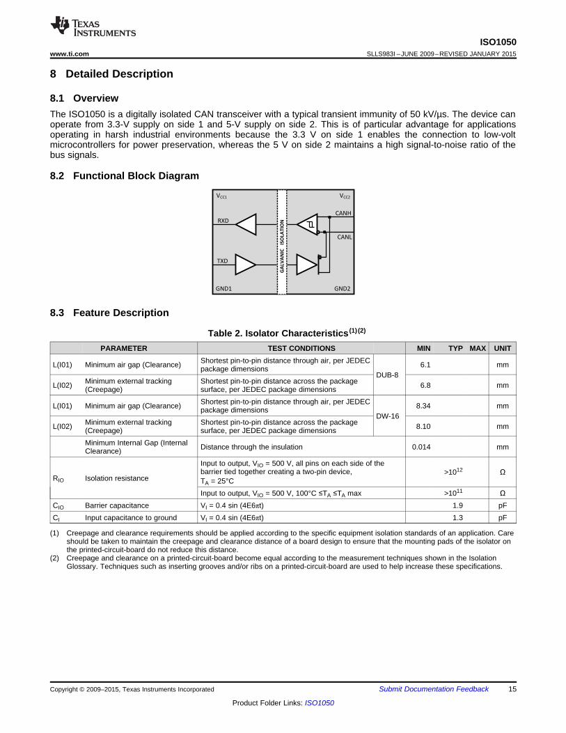
8.1 OverviewThe ISO1050 is a digitally isolated CAN transceiver with a typical transient immunity of 50 kV/µs. The device canoperate from 3.3-V supply on side 1 and 5-V supply on side 2. This is of particular advantage for applicationsoperating in harsh industrial environments because the 3.3 V on side 1 enables the connection to low-voltmicrocontrollers for power preservation, whereas the 5 V on side 2 maintains a high signal-to-noise ratio of thebus signals.
8.2 Functional Block Diagram
8.3 Feature Description
Table 2. Isolator Characteristics (1) (2)
PARAMETER TEST CONDITIONS MIN TYP MAX UNIT
L(I01) Minimum air gap (Clearance) Shortest pin-to-pin distance through air, per JEDECpackage dimensions
DUB-86.1 mm
L(I02) Minimum external tracking(Creepage)
Shortest pin-to-pin distance across the packagesurface, per JEDEC package dimensions 6.8 mm
L(I01) Minimum air gap (Clearance) Shortest pin-to-pin distance through air, per JEDECpackage dimensions
DW-168.34 mm
L(I02) Minimum external tracking(Creepage)
Shortest pin-to-pin distance across the packagesurface, per JEDEC package dimensions 8.10 mm
Minimum Internal Gap (InternalClearance) Distance through the insulation 0.014 mm
RIO Isolation resistance
Input to output, VIO = 500 V, all pins on each side of thebarrier tied together creating a two-pin device,TA = 25°C
>1012 Ω
Input to output, VIO = 500 V, 100°C ≤TA ≤TA max >1011 ΩCIO Barrier capacitance VI = 0.4 sin (4E6πt) 1.9 pFCI Input capacitance to ground VI = 0.4 sin (4E6πt) 1.3 pF

16
ISO1050SLLS983I –JUNE 2009–REVISED JANUARY 2015 www.ti.com
Product Folder Links: ISO1050
Submit Documentation Feedback Copyright © 2009–2015, Texas Instruments Incorporated
Table 3. Insulation CharacteristicsPARAMETER TEST CONDITIONS SPECIFICATION UNIT
VIORM
Maximum working insulationvoltage per DIN V VDE V 0884-10(VDE V 0884-10):2006-12
ISO1050DUB 560Vpeak
ISO1050DW 1200
VPR
Input to output test voltage perDIN V VDE V 0884-10 (VDE V0884-10):2006-12
ISO1050DUB VP R = 1.875 x VIORM, t = 1sec (100% production)Partial discharge < 5 pC
1050Vpeak
ISO1050DW 2250
VIOTM
Transient overvoltage per DIN VVDE V 0884-10 (VDE V 0884-10):2006-12
t = 60 sec (qualification)4000 Vpeakt = 1 sec (100% production)
VISO Isolation voltage per UL 1577ISO1050DUB - Double Protection
t = 60 sec (qualification) 2500Vrms
t = 1 sec (100% production) 3000
ISO1050DW - Single Protectiont = 60 sec (qualification) 4243
Vrmst = 1 sec (100% production) 5092
RS Isolation resistance VIO = 500 V at TS > 109 Ω
Pollution Degree 2
Table 4. IEC 60664-1 RatingsPARAMETER TEST CONDITIONS SPECIFICATION
Basic isolation group Material group II
Installation classification
Rated mains voltage ≤ 150 Vrms I–IVRated mains voltage ≤ 300 Vrms I–IIIRated mains voltage ≤ 400 Vrms I–IIRated mains voltage ≤ 600 Vrms (ISO1050DW only) I-IIRated mains voltage ≤ 848 Vrms (ISO1050DW only) I
(1) Safety limiting intends to prevent potential damage to the isolation barrier upon failure of input or output circuitry. A failure of the I/O canallow low resistance to ground or the supply and, without current limiting dissipate sufficient power to overheat the die and damage theisolation barrier potentially leading to secondary system failures.
Table 5. IEC Safety Limiting Values (1)
PARAMETER TEST CONDITIONS MIN TYP MAX UNIT
IS Safety input, output, or supply currentDUB-8
θJA = 73.3 °C/W, VI = 5.5 V, TJ = 150°C, TA = 25°C 310mA
θJA = 73.3 °C/W, VI = 3.6 V, TJ = 150°C, TA = 25°C 474
DW-16θJA = 76 °C/W, VI = 5.5 V, TJ = 150°C, TA = 25°C 299
mAθJA = 76 °C/W, VI = 3.6 V, TJ = 150°C, TA = 25°C 457
TS Maximum case temperature 150 °C
The safety-limiting constraint is the absolute maximum junction temperature specified in the absolute maximumratings table. The power dissipation and junction-to-air thermal impedance of the device installed in theapplication hardware determines the junction temperature. The assured junction-to-air thermal resistance inThermal Information is that of a device installed on a High-K Test Board for Leaded Surface Mount Packages.The power is the recommended maximum input voltage times the current. The junction temperature is then theambient temperature plus the power times the junction-to-air thermal resistance.

Case Temperature (°C)
Sa
fety
Lim
itin
g C
urr
en
t(m
A)
0 50 100 150 2000
100
200
300
400
500
D001
VCC1 = 3.6 VVCC1 = VCC2 = 5.5 V
Case Temperature (°C)
Sa
fety
Lim
itin
g C
urr
en
t(m
A)
0 50 100 150 2000
100
200
300
400
500
D002
VCC1 = 3.6 VVCC1 = VCC2 = 5.5 V
17
ISO1050www.ti.com SLLS983I –JUNE 2009–REVISED JANUARY 2015
Product Folder Links: ISO1050
Submit Documentation FeedbackCopyright © 2009–2015, Texas Instruments Incorporated
(1) Production tested ≥ 3000 VRMS (ISO1050DUB) and 5092 VRMS (ISO1050DW) for 1 second in accordance with UL 1577.
Figure 21. DUB-8 θJC Thermal Derating Curve perVDE
Figure 22. DW-16 θJC Thermal Derating Curve perVDE
Table 6. Regulatory InformationVDE TUV CSA UL CQC
Certified according to DIN VVDE V 0884-10 (VDE V0884-10):2006-12 & DIN EN61010-1
Certified according to EN/UL/CSA60950-1
Approved under CSAComponent AcceptanceNotice 5A
Recognized under 1577Component RecognitionProgram (1)
Certified according toGB4943.1-2011
Basic InsulationTransient Overvoltage, 4000VPKSurge Voltage, 4000 VPKMaximum Working Voltage,1200 VPK (ISO1050DW) and560 VPK (ISO1050DUB)
ISO1050DW:5000 VRMS Reinforced Insulation,400 VRMS maximum workingvoltage5000 VRMS Basic Insulation,600 VRMS maximum workingvoltageISO1050DUB:2500 VRMS Reinforced Insulation,400 VRMS maximum workingvoltage2500 VRMS Basic Insulation,600 VRMS maximum workingvoltage
5000 VRMS ReinforcedInsulation2 Means of PatientProtection at 125 VRMS perIEC 60601-1 (3rd Ed.)
ISO1050DUB: 2500 VRMSDouble ProtectionISO1050DW: 3500 VRMSDouble Protection,4243 VRMS Single Protection
ISO1050DW:Reinforced Insulation,Altitude ≤ 5000 m, TropicalClimate, 250 VRMS maximumworking voltage
Certificate number:40016131
Certificate number: U8V 11 0977311 008
Master contract number:220991
File number: E181974 Certificate number:CQC14001109541
8.3.1 CAN Bus StatesThe CAN bus has two states during operation: dominant and recessive. A dominant bus state, equivalent to logiclow, is when the bus is driven differentially by a driver. A recessive bus state is when the bus is biased to acommon mode of VCC / 2 through the high-resistance internal input resistors of the receiver, equivalent to a logichigh. The host microprocessor of the CAN node will use the TXD pin to drive the bus and will receive data fromthe bus on the RXD pin. See Figure 23 and Figure 24.

RXDVCC/2
CANH
CANL
GA
LVA
NIC
IS
OLA
TIO
N
Recessive
Logic H
Dominant
Logic L
Recessive
Logic H
Time, t
Ty
pic
al
Bu
sV
olt
ag
e(V
)
Normal & Silent Mode
CANL
CANH
Vdiff(D)
Vdiff(R)
4
3
2
1
18
ISO1050SLLS983I –JUNE 2009–REVISED JANUARY 2015 www.ti.com
Product Folder Links: ISO1050
Submit Documentation Feedback Copyright © 2009–2015, Texas Instruments Incorporated
Figure 23. Bus States (Physical Bit Representation)
Figure 24. Simplified Recessive Common Mode Bias and Receiver
8.3.2 Digital Inputs and OutputsTXD (Input) and RXD (Output):VCC1 for the isolated digital input and output side of the device maybe supplied by a 3.3-V or 5-V supply and thusthe digital inputs and outputs are 3.3-V and 5-V compatible.
NOTETXD is very weakly internally pulled up to VCC1. An external pullup resistor should be usedto make sure that TXD is biased to recessive (high) level to avoid issues on the bus if themicroprocessor doesn't control the pin and TXD floats. TXD pullup strength and CAN bittiming require special consideration when the device is used with an open-drain TXDoutput on the CAN controller of the microprocessor. An adequate external pullup resistormust be used to ensure that the TXD output of the microprocessor maintains adequate bittiming input to the input on the transceiver.
8.3.3 Protection Features
8.3.3.1 TXD Dominant Time-Out (DTO)TXD DTO circuit prevents the local node from blocking network communication in the event of a hardware orsoftware failure where TXD is held dominant longer than the time-out period tTXD_DTO. The TXD DTO circuit timerstarts on a falling edge on TXD. The TXD DTO circuit disables the CAN bus driver if no rising edge is seenbefore the time-out period expires. This frees the bus for communication between other nodes on the network.The CAN driver is re-activated when a recessive signal is seen on the TXD pin, thus clearing the TXD DTOcondition. The receiver and RXD pin still reflect the CAN bus, and the bus pins are biased to recessive levelduring a TXD dominant time-out.

Normal CAN
communication
CAN Bus
Signal
TXD fault stuck dominant: example PCB failure or
bad software
Fault is repaired and local node
transmission capability restored
TXD
%XVZRXOGEH³VWXFNGRPLQDQW´EORFNLQJ
communication for the whole network but TXD DTO prevents this and frees the bus for communication after the time tTXD_DTO.
tTXD_DTO
Communication from
repaired local node
Communication from other
network nodes
TX
D IN
PU
T
CA
N B
US
OU
TP
UT
W
ITH
TX
D D
TO
19
ISO1050www.ti.com SLLS983I –JUNE 2009–REVISED JANUARY 2015
Product Folder Links: ISO1050
Submit Documentation FeedbackCopyright © 2009–2015, Texas Instruments Incorporated
NOTEThe minimum dominant TXD time allowed by the TXD DTO circuit limits the minimumpossible transmitted data rate of the device. The CAN protocol allows a maximum ofeleven successive dominant bits (on TXD) for the worst case, where five successivedominant bits are followed immediately by an error frame. This, along with the tTXD_DTOminimum, limits the minimum data rate. Calculate the minimum transmitted data rate by:Minimum Data Rate = 11 / tTXD_DTO.
Figure 25. Example Timing Diagram for Devices With TXD DTO
8.3.3.2 Thermal ShutdownIf the junction temperature of the device exceeds the thermal shut down threshold the device turns off the CANdriver circuits thus blocking the TXD to bus transmission path. The shutdown condition is cleared when thejunction temperature drops below the thermal shutdown temperature of the device. If the fault condition is stillpresent, the temperature may rise again and the device would enter thermal shut down again. Prolongedoperation with thermal shutdown conditions may affect device reliability.
NOTEDuring thermal shutdown the CAN bus drivers turn off; thus no transmission is possiblefrom TXD to the bus. The CAN bus pins are biased to recessive level during a thermalshutdown, and the receiver to RXD path remains operational.
8.3.3.3 Undervoltage Lockout and Fail-SafeThe supply pins have undervoltage detection that places the device in protected or fail-safe mode. This protectsthe bus during an undervoltage event on VCC1 or VCC2 supply pins. If the bus-side power supply Vcc2 is lowerthan about 2.7V, the power shutdown circuits in the ISO1050 will disable the transceiver to prevent falsetransmissions due to an unstable supply. If Vcc1 is still active when this occurs, the receiver output (RXD) will goto a fail-safe HIGH (recessive) value in about 6 microseconds.
Table 7. Undervoltage Lockout and Fail-SafeVCC1 VCC2 DEVICE STATE BUS OUTPUT RXD
GOOD GOOD Functional Per Device State and TXD Mirrors BusBAD GOOD Protected Recessive High Impedance (3-state)
GOOD BAD Protected High Impedance Recessive (Fail-Safe High)
space
NOTEAfter an undervoltage condition is cleared and the supplies have returned to valid levels,the device typically resumes normal operation in 300 µs

20
ISO1050SLLS983I –JUNE 2009–REVISED JANUARY 2015 www.ti.com
Product Folder Links: ISO1050
Submit Documentation Feedback Copyright © 2009–2015, Texas Instruments Incorporated
8.3.3.4 Floating PinsPullups and pulldowns should be used on critical pins to place the device into known states if the pins float. TheTXD pin should be pulled up through a resistor to VCC1 to force a recessive input level if the microprocessoroutput to the pin floats.
8.3.3.5 CAN Bus Short-Circuit Current LimitingThe device has several protection features that limit the short-circuit current when a CAN bus line is shorted.These include driver current limiting (dominant and recessive). The device has TXD dominant state time out toprevent permanent higher short-circuit current of the dominant state during a system fault. During CANcommunication the bus switches between dominant and recessive states with the data and control fields bits,thus the short-circuit current may be viewed either as the instantaneous current during each bus state, or as aDC average current. For system current (power supply) and power considerations in the termination resistorsand common-mode choke ratings, use the average short-circuit current. Determine the ratio of dominant andrecessive bits by the data in the CAN frame plus the following factors of the protocol and PHY that force eitherrecessive or dominant at certain times:
• Control fields with set bits• Bit-stuffing• Interframe space• TXD dominant time-out (fault case limiting)
These ensure a minimum recessive amount of time on the bus even if the data field contains a high percentageof dominant bits.
NOTEThe short-circuit current of the bus depends on the ratio of recessive to dominant bits andtheir respective short-circuit currents. The average short-circuit current may be calculatedwith the following formula:
IOS(AVG) = %Transmit × [(%REC_Bits × IOS(SS)_REC) + (%DOM_Bits × IOS(SS)_DOM)] +[%Receive × IOS(SS)_REC]
Where• IOS(AVG) is the average short-circuit current.• %Transmit is the percentage the node is transmitting CAN messages.• %Receive is the percentage the node is receiving CAN messages.• %REC_Bits is the percentage of recessive bits in the transmitted CAN messages.• %DOM_Bits is the percentage of dominant bits in the transmitted CAN messages.• IOS(SS)_REC is the recessive steady state short-circuit current.• IOS(SS)_DOM is the dominant steady state short-circuit current.
NOTEConsider the short.circuit current and possible fault cases of the network when sizing thepower ratings of the termination resistance and other network components.
8.4 Device Functional Modes
(1) H = high level, L = low level, Z = common mode (recessive) bias to VCC / 2. See Figure 23 andFigure 24 for bus state and common mode bias information.
Table 8. Driver Function TableINPUT OUTPUTS
DRIVEN BUS STATETXD (1) CANH (1) CANL (1)
L H L DominantH Z Z Recessive

RXD Output
Vcc2
CANL
CANH and CANL Outputs
CANH Input
Vcc2
Input
TXD Input
CANL Input
Vcc2
Input
CANH
10 kW
20 kW
10 kW
10 kW
10 kW
20 kW
OUT
8 W
13 W
IN
1 MW
500 W
VCC1 VCC1 VCC1
VCC1
21
ISO1050www.ti.com SLLS983I –JUNE 2009–REVISED JANUARY 2015
Product Folder Links: ISO1050
Submit Documentation FeedbackCopyright © 2009–2015, Texas Instruments Incorporated
(1) H = high level, L = low level, ? = indeterminate.
Table 9. Receiver Function Table
DEVICE MODE CAN DIFFERENTIAL INPUTSVID = VCANH – VCANL
BUS STATE RXD PIN (1)
Normal or Silent
VID ≥ 0.9 V Dominant L0.5 V < VID < 0.9 V ? ?
VID ≤ 0.5 V Recessive HOpen (VID ≈ 0 V) Open H
(1) H = high level; L = low level; X = irrelevant; ? = indeterminate; Z = high impedance(2) Logic low pulses to prevent dominant time-out.
Table 10. Function Table (1)
DRIVER RECEIVERINPUTS OUTPUTS
BUS STATEDIFFERENTIAL INPUTS
VID = CANH–CANLOUTPUT
RXD BUS STATETXD CANH CANLL (2) H L DOMINANT VID ≥ 0.9 V L DOMINANTH Z Z RECESSIVE 0.5 V < VID < 0.9 V ? ?
Open Z Z RECESSIVE VID ≤ 0.5 V H RECESSIVEX Z Z RECESSIVE Open H RECESSIVE
Figure 26. Equivalent I/O Schematics

1
2
3
4
5
6
7
8
14
13
12
9,10
IN
EN
GND NC
OUT1
3
5
42
ISO1050
TPS76350
RXD
VCC1
NC
TXD
GND1
GND1
GND1
NC
NC
CANH
GND2
4
3
2 6
51
CANL
NC11
7
8
16VCC2
15
RXD
TXDMCU
Vdd
DGND
PSU
L1
N
PE
3.3V
0V
Protective
Earth
Chasis
GroundDigital
Ground
ISO
Ground
Optional Bus
protection
function
SN6501
VCC
D2
D1
GND2
GND1
Galvanic
Isolation
Barrier
22
ISO1050SLLS983I –JUNE 2009–REVISED JANUARY 2015 www.ti.com
Product Folder Links: ISO1050
Submit Documentation Feedback Copyright © 2009–2015, Texas Instruments Incorporated
9 Application and Implementation
NOTEInformation in the following applications sections is not part of the TI componentspecification, and TI does not warrant its accuracy or completeness. TI’s customers areresponsible for determining suitability of components for their purposes. Customers shouldvalidate and test their design implementation to confirm system functionality.
9.1 Application InformationISO1050 can be used with other components from TI such as a microcontroller, a transformer driver, and a linearvoltage regulator to form a fully isolated CAN interface.
9.2 Typical Application
Figure 27. Application Circuit
9.2.1 Design RequirementsUnlike optocoupler-based solution, which needs several external components to improve performance, providebias, or limit current, ISO1050 only needs two external bypass capacitors to operate.
9.2.2 Detailed Design Procedure
9.2.2.1 Bus Loading, Length and Number of NodesThe ISO11898 Standard specifies a maximum bus length of 40 m and maximum stub length of 0.3 m with amaximum of 30 nodes. However, with careful design, users can have longer cables, longer stub lengths, andmany more nodes to a bus. A high number of nodes requires a transceiver with high input impedance such asthe ISO1050.

MCU or DSP
CANController
CANTransceiver
Node 1
MCU or DSP
CANController
CANTransceiver
Node 2
MCU or DSP
CANController
CANTransceiver
Node 3
MCU or DSP
CANController
CANTransceiver
Node n
(with termination)
RTERM
RTERM
23
ISO1050www.ti.com SLLS983I –JUNE 2009–REVISED JANUARY 2015
Product Folder Links: ISO1050
Submit Documentation FeedbackCopyright © 2009–2015, Texas Instruments Incorporated
Typical Application (continued)Many CAN organizations and standards have scaled the use of CAN for applications outside the originalISO11898 standard. They have made system level trade offs for data rate, cable length, and parasitic loading ofthe bus. Examples of some of these specifications are ARINC825, CANopen, CAN Kingdom, DeviceNet andNMEA200.
A CAN network design is a series of tradeoffs, but these devices operate over wide –12-V to 12-V common-mode range. In ISO11898-2 the driver differential output is specified with a 60-Ω load (the two 120-Ω terminationresistors in parallel) and the differential output must be greater than 1.5 V. The ISO1050 is specified to meet the1.5-V requirement with a 60-Ω load, and additionally specified with a differential output of 1.4 V with a 45-Ω load.The differential input resistance of the ISO1050 is a minimum of 30 kΩ. If 167 ISO1050 transceivers are inparallel on a bus, this is equivalent to a 180-Ω differential load. That transceiver load of 180 Ω in parallel with the60 Ω gives a total 45 Ω. Therefore, the ISO1050 theoretically supports over 167 transceivers on a single bussegment with margin to the 1.2-V minimum differential input at each node. However for CAN network designmargin must be given for signal loss across the system and cabling, parasitic loadings, network imbalances,ground offsets and signal integrity thus a practical maximum number of nodes is typically much lower. Bus lengthmay also be extended beyond the original ISO11898 standard of 40 m by careful system design and data ratetradeoffs. For example, CAN open network design guidelines allow the network to be up to 1km with changes inthe termination resistance, cabling, less than 64 nodes and significantly lowered data rate.
This flexibility in CAN network design is one of the key strengths of the various extensions and additionalstandards that have been built on the original ISO11898 CAN standard. In using this flexibility comes theresponsibility of good network design.
9.2.2.2 CAN TerminationThe ISO11898 standard specifies the interconnect to be a single twisted pair cable (shielded or unshielded) with120-Ω characteristic impedance (ZO). Resistors equal to the characteristic impedance of the line should be usedto terminate both ends of the cable to prevent signal reflections. Unterminated drop-lines (stubs) connectingnodes to the bus should be kept as short as possible to minimize signal reflections. The termination may be in anode, but if nodes may be removed from the bus, the termination must be carefully placed so that it is notremoved from the bus.
Figure 28. Typical CAN Bus
Termination may be a single 120-Ω resistor at the end of the bus, either on the cable or in a terminating node. Iffiltering and stabilization of the common mode voltage of the bus is desired, then split termination may be used.(See Figure 29). Split termination improves the electromagnetic emissions behavior of the network by eliminatingfluctuations in the bus common-mode voltages at the start and end of message transmissions.

10
100
0 250 500 750 1000
V – Working Voltage – VIORM
Life E
xpecta
ncy
–Y
ears
880120
V at 560 VIORM28 Years
G001
CAN
Transceiver
CANL
CANH
CSPLIT
CAN
TransceiverRTERM
Standard Termination Split Termination
CANL
CANH
R /2TERM
R /2TERM
24
ISO1050SLLS983I –JUNE 2009–REVISED JANUARY 2015 www.ti.com
Product Folder Links: ISO1050
Submit Documentation Feedback Copyright © 2009–2015, Texas Instruments Incorporated
Typical Application (continued)
Figure 29. CAN Bus Termination Concepts
9.2.3 Application Curve
Figure 30. Life Expectancy vs Working Voltage (ISO1050DUB)

10 mils
10 mils
40 milsFR-4
0r ~ 4.5
Keep this
space free
from planes,
traces, pads,
and vias
Ground plane
Power plane
Low-speed traces
High-speed traces
25
ISO1050www.ti.com SLLS983I –JUNE 2009–REVISED JANUARY 2015
Product Folder Links: ISO1050
Submit Documentation FeedbackCopyright © 2009–2015, Texas Instruments Incorporated
10 Power Supply RecommendationsTo ensure reliable operation at all data rates and supply voltages, a 0.1-µF bypass capacitor is recommended atinput and output supply pins (VCC1 and VCC2). The capacitors should be placed as close to the supply pins aspossible. If only a single primary-side power supply is available in an application, isolated power can begenerated for the secondary-side with the help of a transformer driver such as TI's SN6501. For suchapplications, detailed power supply design and transformer selection recommendations are available in SN6501data sheet (SLLSEA0).
11 Layout
11.1 Layout GuidelinesA minimum of four layers is required to accomplish a low EMI PCB design (see Figure 31). Layer stacking shouldbe in the following order (top-to-bottom): high-speed signal layer, ground plane, power plane and low-frequencysignal layer.• Routing the high-speed traces on the top layer avoids the use of vias (and the introduction of their
inductances) and allows for clean interconnects between the isolator and the transmitter and receiver circuitsof the data link.
• Placing a solid ground plane next to the high-speed signal layer establishes controlled impedance fortransmission line interconnects and provides an excellent low-inductance path for the return current flow.
• Placing the power plane next to the ground plane creates additional high-frequency bypass capacitance ofapproximately 100 pF/in2.
• Routing the slower speed control signals on the bottom layer allows for greater flexibility as these signal linksusually have margin to tolerate discontinuities such as vias.
If an additional supply voltage plane or signal layer is needed, add a second power / ground plane system to thestack to keep it symmetrical. This makes the stack mechanically stable and prevents it from warping. Also thepower and ground plane of each power system can be placed closer together, thus increasing the high-frequencybypass capacitance significantly.
For detailed layout recommendations, see Application Note SLLA284, Digital Isolator Design Guide.
11.1.1 PCB MaterialFor digital circuit boards operating below 150 Mbps, (or rise and fall times higher than 1 ns), and trace lengths ofup to 10 inches, use standard FR-4 epoxy-glass as PCB material. FR-4 (Flame Retardant 4) meets therequirements of Underwriters Laboratories UL94-V0, and is preferred over cheaper alternatives due to its lowerdielectric losses at high frequencies, less moisture absorption, greater strength and stiffness, and its self-extinguishing flammability-characteristics.
11.2 Layout Example
Figure 31. Recommended Layer Stack

26
ISO1050SLLS983I –JUNE 2009–REVISED JANUARY 2015 www.ti.com
Product Folder Links: ISO1050
Submit Documentation Feedback Copyright © 2009–2015, Texas Instruments Incorporated
12 Device and Documentation Support
12.1 Documentation Support
12.1.1 Related Documentation• High-Voltage Lifetime of the ISO72x Family of Digital Isolators (SLLA197)• Transformer Driver for Isolated Power Supplies (SLLSEA0)• Digital Isolator Design Guide (SLLA284)• Isolation Glossary (SLLA353)
12.2 TrademarksAll trademarks are the property of their respective owners.
12.3 Electrostatic Discharge CautionThese devices have limited built-in ESD protection. The leads should be shorted together or the device placed in conductive foamduring storage or handling to prevent electrostatic damage to the MOS gates.
12.4 GlossarySLYZ022 — TI Glossary.
This glossary lists and explains terms, acronyms, and definitions.
13 Mechanical, Packaging, and Orderable InformationThe following pages include mechanical, packaging, and orderable information. This information is the mostcurrent data available for the designated devices. This data is subject to change without notice and revision ofthis document. For browser-based versions of this data sheet, refer to the left-hand navigation.

www.ti.com
PACKAGE OUTLINE
C
TYP10.639.97
2.65 MAX
14X 1.27
16X0.510.31
2X
8.89
TYP0.330.10
0 - 80.30.1
(1.4)
0.25
GAGE PLANE
1.270.40
A
NOTE 3
10.510.1
B
NOTE 4
7.67.4
4221009/B 07/2016
SOIC - 2.65 mm max heightDW0016BSOIC
NOTES:
1. All linear dimensions are in millimeters. Dimensions in parenthesis are for reference only. Dimensioning and tolerancingper ASME Y14.5M.
2. This drawing is subject to change without notice.3. This dimension does not include mold flash, protrusions, or gate burrs. Mold flash, protrusions, or gate burrs shall not
exceed 0.15 mm, per side.4. This dimension does not include interlead flash. Interlead flash shall not exceed 0.25 mm, per side.5. Reference JEDEC registration MS-013.
116
0.25 C A B
98
PIN 1 IDAREA
SEATING PLANE
0.1 C
SEE DETAIL A
TYPICALDETAIL A
SCALE 1.500
27
ISO1050www.ti.com SLLS983I –JUNE 2009–REVISED JANUARY 2015
Product Folder Links: ISO1050
Submit Documentation FeedbackCopyright © 2009–2015, Texas Instruments Incorporated

www.ti.com
EXAMPLE BOARD LAYOUT
(9.75)R0.05 TYP
0.07 MAXALL AROUND
0.07 MINALL AROUND
(9.3)
14X (1.27)
R0.05 TYP
16X (1.65)
16X (0.6)
14X (1.27)
16X (2)
16X (0.6)
4221009/B 07/2016
SYMM
SOIC - 2.65 mm max heightDW0016BSOIC
SYMM
SEEDETAILS
1
8 9
16
SYMM
HV / ISOLATION OPTION8.1 mm CLEARANCE/CREEPAGE
NOTES: (continued)
6. Publication IPC-7351 may have alternate designs.7. Solder mask tolerances between and around signal pads can vary based on board fabrication site.
METALSOLDER MASKOPENING
NON SOLDER MASKDEFINED
SOLDER MASK DETAILS
OPENINGSOLDER MASK METAL
SOLDER MASKDEFINED
SCALE:4XLAND PATTERN EXAMPLE
SYMM
1
8 9
16
IPC-7351 NOMINAL7.3 mm CLEARANCE/CREEPAGE
SEEDETAILS
28
ISO1050SLLS983I –JUNE 2009–REVISED JANUARY 2015 www.ti.com
Product Folder Links: ISO1050
Submit Documentation Feedback Copyright © 2009–2015, Texas Instruments Incorporated

www.ti.com
EXAMPLE STENCIL DESIGN
R0.05 TYPR0.05 TYP
16X (1.65)
16X (0.6)
14X (1.27)
(9.75)
16X (2)
16X (0.6)
14X (1.27)
(9.3)
4221009/B 07/2016
SOIC - 2.65 mm max heightDW0016BSOIC
NOTES: (continued)
8. Laser cutting apertures with trapezoidal walls and rounded corners may offer better paste release. IPC-7525 may have alternatedesign recommendations.
9. Board assembly site may have different recommendations for stencil design.
SYMM
SYMM
1
8 9
16
HV / ISOLATION OPTION8.1 mm CLEARANCE/CREEPAGE
BASED ON 0.125 mm THICK STENCILSOLDER PASTE EXAMPLE
SCALE:4X
SYMM
SYMM
1
8 9
16
IPC-7351 NOMINAL7.3 mm CLEARANCE/CREEPAGE
29
ISO1050www.ti.com SLLS983I –JUNE 2009–REVISED JANUARY 2015
Product Folder Links: ISO1050
Submit Documentation FeedbackCopyright © 2009–2015, Texas Instruments Incorporated
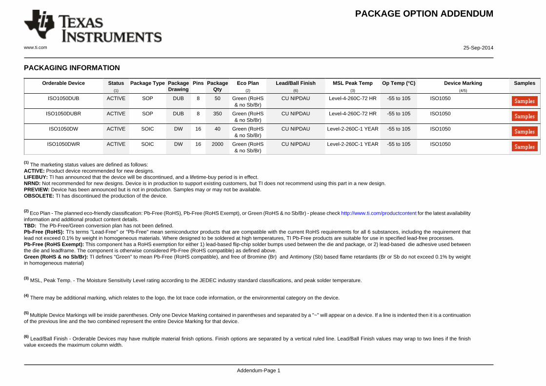
PACKAGE OPTION ADDENDUM
www.ti.com 25-Sep-2014
Addendum-Page 1
PACKAGING INFORMATION
Orderable Device Status(1)
Package Type PackageDrawing
Pins PackageQty
Eco Plan(2)
Lead/Ball Finish(6)
MSL Peak Temp(3)
Op Temp (°C) Device Marking(4/5)
Samples
ISO1050DUB ACTIVE SOP DUB 8 50 Green (RoHS& no Sb/Br)
CU NIPDAU Level-4-260C-72 HR -55 to 105 ISO1050
ISO1050DUBR ACTIVE SOP DUB 8 350 Green (RoHS& no Sb/Br)
CU NIPDAU Level-4-260C-72 HR -55 to 105 ISO1050
ISO1050DW ACTIVE SOIC DW 16 40 Green (RoHS& no Sb/Br)
CU NIPDAU Level-2-260C-1 YEAR -55 to 105 ISO1050
ISO1050DWR ACTIVE SOIC DW 16 2000 Green (RoHS& no Sb/Br)
CU NIPDAU Level-2-260C-1 YEAR -55 to 105 ISO1050
(1) The marketing status values are defined as follows:ACTIVE: Product device recommended for new designs.LIFEBUY: TI has announced that the device will be discontinued, and a lifetime-buy period is in effect.NRND: Not recommended for new designs. Device is in production to support existing customers, but TI does not recommend using this part in a new design.PREVIEW: Device has been announced but is not in production. Samples may or may not be available.OBSOLETE: TI has discontinued the production of the device.
(2) Eco Plan - The planned eco-friendly classification: Pb-Free (RoHS), Pb-Free (RoHS Exempt), or Green (RoHS & no Sb/Br) - please check http://www.ti.com/productcontent for the latest availabilityinformation and additional product content details.TBD: The Pb-Free/Green conversion plan has not been defined.Pb-Free (RoHS): TI's terms "Lead-Free" or "Pb-Free" mean semiconductor products that are compatible with the current RoHS requirements for all 6 substances, including the requirement thatlead not exceed 0.1% by weight in homogeneous materials. Where designed to be soldered at high temperatures, TI Pb-Free products are suitable for use in specified lead-free processes.Pb-Free (RoHS Exempt): This component has a RoHS exemption for either 1) lead-based flip-chip solder bumps used between the die and package, or 2) lead-based die adhesive used betweenthe die and leadframe. The component is otherwise considered Pb-Free (RoHS compatible) as defined above.Green (RoHS & no Sb/Br): TI defines "Green" to mean Pb-Free (RoHS compatible), and free of Bromine (Br) and Antimony (Sb) based flame retardants (Br or Sb do not exceed 0.1% by weightin homogeneous material)
(3) MSL, Peak Temp. - The Moisture Sensitivity Level rating according to the JEDEC industry standard classifications, and peak solder temperature.
(4) There may be additional marking, which relates to the logo, the lot trace code information, or the environmental category on the device.
(5) Multiple Device Markings will be inside parentheses. Only one Device Marking contained in parentheses and separated by a "~" will appear on a device. If a line is indented then it is a continuationof the previous line and the two combined represent the entire Device Marking for that device.
(6) Lead/Ball Finish - Orderable Devices may have multiple material finish options. Finish options are separated by a vertical ruled line. Lead/Ball Finish values may wrap to two lines if the finishvalue exceeds the maximum column width.
PACKAGE OPTION ADDENDUM
www.ti.com 25-Sep-2014
Addendum-Page 2
Important Information and Disclaimer:The information provided on this page represents TI's knowledge and belief as of the date that it is provided. TI bases its knowledge and belief on informationprovided by third parties, and makes no representation or warranty as to the accuracy of such information. Efforts are underway to better integrate information from third parties. TI has taken andcontinues to take reasonable steps to provide representative and accurate information but may not have conducted destructive testing or chemical analysis on incoming materials and chemicals.TI and TI suppliers consider certain information to be proprietary, and thus CAS numbers and other limited information may not be available for release.
In no event shall TI's liability arising out of such information exceed the total purchase price of the TI part(s) at issue in this document sold by TI to Customer on an annual basis.

TAPE AND REEL INFORMATION
*All dimensions are nominal
Device PackageType
PackageDrawing
Pins SPQ ReelDiameter
(mm)
ReelWidth
W1 (mm)
A0(mm)
B0(mm)
K0(mm)
P1(mm)
W(mm)
Pin1Quadrant
ISO1050DUBR SOP DUB 8 350 330.0 24.4 10.9 10.01 5.85 16.0 24.0 Q1
ISO1050DWR SOIC DW 16 2000 330.0 16.4 10.75 10.7 2.7 12.0 16.0 Q1
PACKAGE MATERIALS INFORMATION
www.ti.com 3-Aug-2017
Pack Materials-Page 1

*All dimensions are nominal
Device Package Type Package Drawing Pins SPQ Length (mm) Width (mm) Height (mm)
ISO1050DUBR SOP DUB 8 350 346.0 346.0 41.0
ISO1050DWR SOIC DW 16 2000 367.0 367.0 38.0
PACKAGE MATERIALS INFORMATION
www.ti.com 3-Aug-2017
Pack Materials-Page 2

www.ti.com
PACKAGE OUTLINE
C10.710.1 TYP
6X 2.54
4X(1.524)
2X7.62
0.3550.204 TYP
0 - 4
8X 0.5550.355
6.626.52
0.38 MIN
0.635GAGE PLANE
4.85 MAX
1.451.15
A
9.559.02
NOTE 3
B 6.676.57
4X (0.99)
4222355/D 08/2017
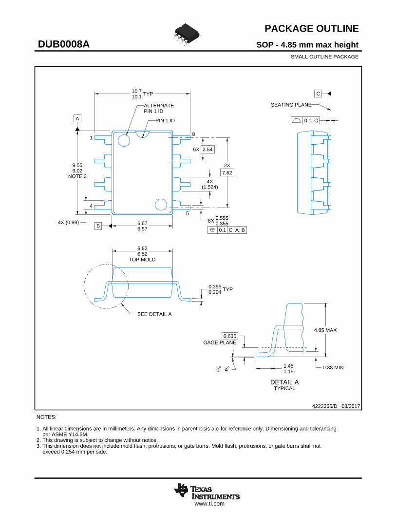
SOP - 4.85 mm max heightDUB0008ASMALL OUTLINE PACKAGE
NOTES: 1. All linear dimensions are in millimeters. Any dimensions in parenthesis are for reference only. Dimensioning and tolerancing per ASME Y14.5M. 2. This drawing is subject to change without notice. 3. This dimension does not include mold flash, protrusions, or gate burrs. Mold flash, protrusions, or gate burrs shall not exceed 0.254 mm per side.
18
0.1 C A B
54
PIN 1 ID
ALTERNATEPIN 1 ID
SEATING PLANE
0.1 C
SEE DETAIL A
TOP MOLD
DETAIL ATYPICAL
SCALE 1.200

www.ti.com
EXAMPLE BOARD LAYOUT
(9.1)
0.07 MAXALL AROUND
0.07 MINALL AROUND
8X (2.35)
8X (0.65)
6X (2.54)
(R0.05)TYP
4222355/D 08/2017
SOP - 4.85 mm max heightDUB0008ASMALL OUTLINE PACKAGE
SYMM
SYMM
LAND PATTERN EXAMPLEEXPOSED METAL SHOWN
SCALE:5X
1
45
8
NOTES: (continued) 4. Publication IPC-7351 may have alternate designs. 5. Solder mask tolerances between and around signal pads can vary based on board fabrication site.
METALSOLDER MASKOPENING
NON SOLDER MASKDEFINED
SOLDER MASK DETAILSNOT TO SCALE
EXPOSED METAL
SOLDER MASKOPENING
METAL UNDERSOLDER MASK
SOLDER MASKDEFINED
EXPOSED METAL

www.ti.com
EXAMPLE STENCIL DESIGN
(9.1)
6X (2.54)
8X (0.65)
8X (2.35)(R0.05) TYP
4222355/D 08/2017
SOP - 4.85 mm max heightDUB0008ASMALL OUTLINE PACKAGE
NOTES: (continued) 6. Laser cutting apertures with trapezoidal walls and rounded corners may offer better paste release. IPC-7525 may have alternate design recommendations. 7. Board assembly site may have different recommendations for stencil design.
SYMM
SYMM
1
45
8
SOLDER PASTE EXAMPLEBASED ON 0.125 mm THICK STENCIL
SCALE:5X

IMPORTANT NOTICE
Texas Instruments Incorporated (TI) reserves the right to make corrections, enhancements, improvements and other changes to itssemiconductor products and services per JESD46, latest issue, and to discontinue any product or service per JESD48, latest issue. Buyersshould obtain the latest relevant information before placing orders and should verify that such information is current and complete.TI’s published terms of sale for semiconductor products (http://www.ti.com/sc/docs/stdterms.htm) apply to the sale of packaged integratedcircuit products that TI has qualified and released to market. Additional terms may apply to the use or sale of other types of TI products andservices.Reproduction of significant portions of TI information in TI data sheets is permissible only if reproduction is without alteration and isaccompanied by all associated warranties, conditions, limitations, and notices. TI is not responsible or liable for such reproduceddocumentation. Information of third parties may be subject to additional restrictions. Resale of TI products or services with statementsdifferent from or beyond the parameters stated by TI for that product or service voids all express and any implied warranties for theassociated TI product or service and is an unfair and deceptive business practice. TI is not responsible or liable for any such statements.Buyers and others who are developing systems that incorporate TI products (collectively, “Designers”) understand and agree that Designersremain responsible for using their independent analysis, evaluation and judgment in designing their applications and that Designers havefull and exclusive responsibility to assure the safety of Designers' applications and compliance of their applications (and of all TI productsused in or for Designers’ applications) with all applicable regulations, laws and other applicable requirements. Designer represents that, withrespect to their applications, Designer has all the necessary expertise to create and implement safeguards that (1) anticipate dangerousconsequences of failures, (2) monitor failures and their consequences, and (3) lessen the likelihood of failures that might cause harm andtake appropriate actions. Designer agrees that prior to using or distributing any applications that include TI products, Designer willthoroughly test such applications and the functionality of such TI products as used in such applications.TI’s provision of technical, application or other design advice, quality characterization, reliability data or other services or information,including, but not limited to, reference designs and materials relating to evaluation modules, (collectively, “TI Resources”) are intended toassist designers who are developing applications that incorporate TI products; by downloading, accessing or using TI Resources in anyway, Designer (individually or, if Designer is acting on behalf of a company, Designer’s company) agrees to use any particular TI Resourcesolely for this purpose and subject to the terms of this Notice.TI’s provision of TI Resources does not expand or otherwise alter TI’s applicable published warranties or warranty disclaimers for TIproducts, and no additional obligations or liabilities arise from TI providing such TI Resources. TI reserves the right to make corrections,enhancements, improvements and other changes to its TI Resources. TI has not conducted any testing other than that specificallydescribed in the published documentation for a particular TI Resource.Designer is authorized to use, copy and modify any individual TI Resource only in connection with the development of applications thatinclude the TI product(s) identified in such TI Resource. NO OTHER LICENSE, EXPRESS OR IMPLIED, BY ESTOPPEL OR OTHERWISETO ANY OTHER TI INTELLECTUAL PROPERTY RIGHT, AND NO LICENSE TO ANY TECHNOLOGY OR INTELLECTUAL PROPERTYRIGHT OF TI OR ANY THIRD PARTY IS GRANTED HEREIN, including but not limited to any patent right, copyright, mask work right, orother intellectual property right relating to any combination, machine, or process in which TI products or services are used. Informationregarding or referencing third-party products or services does not constitute a license to use such products or services, or a warranty orendorsement thereof. Use of TI Resources may require a license from a third party under the patents or other intellectual property of thethird party, or a license from TI under the patents or other intellectual property of TI.TI RESOURCES ARE PROVIDED “AS IS” AND WITH ALL FAULTS. TI DISCLAIMS ALL OTHER WARRANTIES ORREPRESENTATIONS, EXPRESS OR IMPLIED, REGARDING RESOURCES OR USE THEREOF, INCLUDING BUT NOT LIMITED TOACCURACY OR COMPLETENESS, TITLE, ANY EPIDEMIC FAILURE WARRANTY AND ANY IMPLIED WARRANTIES OFMERCHANTABILITY, FITNESS FOR A PARTICULAR PURPOSE, AND NON-INFRINGEMENT OF ANY THIRD PARTY INTELLECTUALPROPERTY RIGHTS. TI SHALL NOT BE LIABLE FOR AND SHALL NOT DEFEND OR INDEMNIFY DESIGNER AGAINST ANY CLAIM,INCLUDING BUT NOT LIMITED TO ANY INFRINGEMENT CLAIM THAT RELATES TO OR IS BASED ON ANY COMBINATION OFPRODUCTS EVEN IF DESCRIBED IN TI RESOURCES OR OTHERWISE. IN NO EVENT SHALL TI BE LIABLE FOR ANY ACTUAL,DIRECT, SPECIAL, COLLATERAL, INDIRECT, PUNITIVE, INCIDENTAL, CONSEQUENTIAL OR EXEMPLARY DAMAGES INCONNECTION WITH OR ARISING OUT OF TI RESOURCES OR USE THEREOF, AND REGARDLESS OF WHETHER TI HAS BEENADVISED OF THE POSSIBILITY OF SUCH DAMAGES.Unless TI has explicitly designated an individual product as meeting the requirements of a particular industry standard (e.g., ISO/TS 16949and ISO 26262), TI is not responsible for any failure to meet such industry standard requirements.Where TI specifically promotes products as facilitating functional safety or as compliant with industry functional safety standards, suchproducts are intended to help enable customers to design and create their own applications that meet applicable functional safety standardsand requirements. Using products in an application does not by itself establish any safety features in the application. Designers mustensure compliance with safety-related requirements and standards applicable to their applications. Designer may not use any TI products inlife-critical medical equipment unless authorized officers of the parties have executed a special contract specifically governing such use.Life-critical medical equipment is medical equipment where failure of such equipment would cause serious bodily injury or death (e.g., lifesupport, pacemakers, defibrillators, heart pumps, neurostimulators, and implantables). Such equipment includes, without limitation, allmedical devices identified by the U.S. Food and Drug Administration as Class III devices and equivalent classifications outside the U.S.TI may expressly designate certain products as completing a particular qualification (e.g., Q100, Military Grade, or Enhanced Product).Designers agree that it has the necessary expertise to select the product with the appropriate qualification designation for their applicationsand that proper product selection is at Designers’ own risk. Designers are solely responsible for compliance with all legal and regulatoryrequirements in connection with such selection.Designer will fully indemnify TI and its representatives against any damages, costs, losses, and/or liabilities arising out of Designer’s non-compliance with the terms and provisions of this Notice.
Mailing Address: Texas Instruments, Post Office Box 655303, Dallas, Texas 75265Copyright © 2017, Texas Instruments Incorporated