is61nlp6432a is61nlp6436a/is61nvp6436a is61nlp12818a/is61nvp12818a · 2013-02-14 · nlp: vdd 3.3v...
TRANSCRIPT

Integrated Silicon Solution, Inc. — www.issi.com — 1-800-379-4774 1Rev. 00A 08/31/05
Copyright © 2005 Integrated Silicon Solution, Inc. All rights reserved. ISSI reserves the right to make changes to this specification and its products at any time without notice. ISSI assumes no liability arising out of the application or use of any information, products or services described herein. Customers are advised to obtain the latest version of this device specification before relying on any published information and before placing orders for products.
IS61NLP6432AIS61NLP6436A/IS61NVP6436AIS61NLP12818A/IS61NVP12818A
FEATURES
• 100percentbusutilization• NowaitcyclesbetweenReadandWrite• Internalself-timedwritecycle• IndividualByteWriteControl• SingleR/W(Read/Write)controlpin• Clockcontrolled,registeredaddress, dataandcontrol
• Interleavedorlinearburstsequencecontrolus-ingMODEinput
• Threechipenablesforsimpledepthexpansionandaddresspipelining
• PowerDownmode• Commondatainputsanddataoutputs• CKEpintoenableclockandsuspendoperation• JEDEC100-pinTQFPpackage• Powersupply:NVP:Vdd 2.5V(±5%),Vddq2.5V(±5%)NLP:Vdd3.3V(±5%),Vddq3.3V/2.5V(±5%)
• Industrialtemperatureavailable• Lead-freeavailable
DESCRIPTION
The2Meg'NLP/NVP'productfamilyfeaturehigh-speed,low-powersynchronousstaticRAMsdesignedtoprovideaburstable,high-performance,'nowait'state,devicefornetworkingandcommunicationsapplications.Theyareorganized as 64Kwords by 32 bits, 64Kwords by 36bits,and128Kwordsby18bits,fabricatedwithISSI'sadvancedCMOStechnology.
Incorporating a 'no wait' state feature, wait cycles areeliminatedwhenthebusswitchesfromreadtowrite,orwritetoread.Thisdeviceintegratesa2-bitburstcounter,high-speedSRAMcore,andhigh-drivecapabilityoutputsintoasinglemonolithiccircuit.
Allsynchronousinputspassthroughregistersarecontrolledbyapositive-edge-triggeredsingleclockinput.Operationsmaybesuspendedandallsynchronous inputs ignoredwhenClockEnable,CKEisHIGH.Inthisstatetheinternaldevicewillholdtheirpreviousvalues.
AllRead,WriteandDeselectcyclesareinitiatedbytheADVinput.WhentheADVisHIGHtheinternalburstcounterisincremented.NewexternaladdressescanbeloadedwhenADVisLOW.
Writecyclesareinternallyself-timedandareinitiatedbytherisingedgeoftheclockinputsandwhenWEisLOW.Separatebyteenablesallowindividualbytestobewritten.
Aburstmodepin(MODE)definestheorderoftheburstsequence.WhentiedHIGH,theinterleavedburstsequenceisselected.WhentiedLOW,thelinearburstsequenceisselected.
64K x 32, 64K x 36, and 128K x 182Mb, PIPELINE 'NO WAIT' STATE BUS SRAM
PRELIMINARY INFORMATIONSEPTEMBER 2005
FAST ACCESS TIME Symbol Parameter -250 -200 Units tkq ClockAccessTime 2.6 3.1 ns tkc CycleTime 4 5 ns Frequency 250 200 MHz

2 Integrated Silicon Solution, Inc. — www.issi.com — 1-800-379-4774Rev. 00A08/31/05
IS61NLP6432AIS61NLP6436A/IS61NVP6436AIS61NLP12818A/IS61NVP12818ABLOCK DIAGRAM
ADVWE BWŸX(X=a,b,c,d or a,b)
CE
CE2
CE2
CONTROLLOGIC
64Kx32;64Kx36;128Kx18
MEMORY ARRAY
WRITEADDRESSREGISTER
WRITEADDRESSREGISTER
CONTROLLOGIC
OUTPUTREGISTER
BUFFER
ADDRESSREGISTER
x 32/x 36: A [0:15] orx 18: A [0:16]
CLK
CKE
A2-A15 or A2-A16
A0-A1 A'0-A'1
BURSTADDRESSCOUNTER
MODE
DATA-INREGISTER
DATA-INREGISTER
CONTROLREGISTER
OEZZ
32, 36 or 18
K
K
DQx/DQPx
K
K

Integrated Silicon Solution, Inc. — www.issi.com — 1-800-379-4774 3Rev. 00A08/31/05
IS61NLP6432AIS61NLP6436A/IS61NVP6436AIS61NLP12818A/IS61NVP12818APIN CONFIGURATION100-Pin TQFP
64K x 32
123456789101112131415161718192021222324252627282930
807978777675747372717069686766656463626160595857565554535251
100 99 98 97 96 95 94 93 92 91 90 89 88 87 86 85 84 83 82 81
31 32 33 34 35 36 37 38 39 40 41 42 43 44 45 46 47 48 49 50
DQPb
DQb
DQb
VDDQ
Vss
DQbDQb
DQb
DQb
Vss
VDDQ
DQb
DQbVssNCVDD
ZZ
DQa
DQa
VDDQ
Vss
DQa
DQa
DQaDQaVss
VDDQ
DQaDQaDQPa
DQPc
DQc
DQc
VDDQ
Vss
DQcDQc
DQc
DQc
Vss
VDDQ
DQc
DQcNC
VDD
NC
Vss
DQd
DQd
VDDQ
VssDQd
DQd
DQdDQdVss
VDDQ
DQdDQd
DQPd
A
A CE
CE
2
BWd
BWc
BWb
BWa
CE2
VD
D
Vss
CLKWE
CKE
OE
AD
VN
C
NC
A A
MO
DE A A A A A1
A0
NC
NC
Vss
VD
D
NC
NC A A A A A A
NC
64K x 36
PIN DESCRIPTIONSA0, A1 Synchronous Address Inputs. These
pins must tied to the two LSBs of the address bus.
A Synchronous Address Inputs
CLK Synchronous Clock
ADV Synchronous Burst Address Advance
BWa-BWd Synchronous Byte Write Enable
WE Write Enable
CKE Clock Enable
Vss Ground for Core
NC Not Connected
CE, CE2, CE2 Synchronous Chip Enable
OE Output Enable
DQa-DQd Synchronous Data Input/Output
DQPa-DQPd Parity Data I/O
MODE Burst Sequence Selection
Vdd +3.3V/2.5V Power Supply
Vss Ground for output Buffer
Vddq Isolated Output Buffer Supply: +3.3V/2.5V
ZZ Snooze Enable
123456789101112131415161718192021222324252627282930
807978777675747372717069686766656463626160595857565554535251
100 99 98 97 96 95 94 93 92 91 90 89 88 87 86 85 84 83 82 81
31 32 33 34 35 36 37 38 39 40 41 42 43 44 45 46 47 48 49 50
NC
DQb
DQb
VDDQ
Vss
DQbDQb
DQb
DQb
Vss
VDDQ
DQb
DQbVssNCVDD
ZZ
DQa
DQa
VDDQ
Vss
DQa
DQa
DQaDQaVss
VDDQ
DQaDQaNC
NC
DQc
DQc
VDDQ
Vss
DQcDQc
DQc
DQc
Vss
VDDQ
DQc
DQcNC
VDD
NC
Vss
DQd
DQd
VDDQ
VssDQd
DQd
DQdDQdVss
VDDQ
DQdDQd
NC
A
A CE
CE
2
BWd
BWc
BWb
BWa
CE2
VD
D
Vss
CLKWE
CKE
OE
AD
VN
C
NC
A A
MO
DE A A A A A1
A0
NC
NC
Vss
VD
D
NC
NC A A A A A A
NC

4 Integrated Silicon Solution, Inc. — www.issi.com — 1-800-379-4774Rev. 00A08/31/05
IS61NLP6432AIS61NLP6436A/IS61NVP6436AIS61NLP12818A/IS61NVP12818APIN CONFIGURATION100-Pin TQFP
128K x 18
123456789101112131415161718192021222324252627282930
807978777675747372717069686766656463626160595857565554535251
100 99 98 97 96 95 94 93 92 91 90 89 88 87 86 85 84 83 82 81
31 32 33 34 35 36 37 38 39 40 41 42 43 44 45 46 47 48 49 50
A
NC
NC
VDDQ
Vss
NCDQPa
DQa
DQa
Vss
VDDQ
DQa
DQaVssNCVDD
ZZ
DQa
DQa
VDDQ
Vss
DQa
DQa
NCNC
Vss
VDDQ
NCNCNC
NC
NC
NC
VDDQ
Vss
NCNC
DQb
DQb
Vss
VDDQ
DQb
DQbNC
VDD
NCVss
DQb
DQb
VDDQ
VssDQb
DQb
DQPbNC
Vss
VDDQ
NCNCNC
A A CE
CE
2
NC
NCBWb
BWa
CE2
VD
D
Vss
CLKWE
CKE
OE
AD
VN
C
NC
A A
MO
DE A A A A A1
A0
NC
NC
Vss
VD
D
NC
NC A A A A A A
NC
PIN DESCRIPTIONSA0, A1 Synchronous Address Inputs. These
pins must tied to the two LSBs of the address bus.
A Synchronous Address Inputs
CLK Synchronous Clock
ADV Synchronous Burst Address Advance
BWa-BWd Synchronous Byte Write Enable
WE Write Enable
CKE Clock Enable
Vss Ground for Core
NC Not Connected
CE, CE2, CE2 Synchronous Chip Enable
OE Output Enable
DQa-DQd Synchronous Data Input/Output
DQPa-DQPd Parity Data I/O
MODE Burst Sequence Selection
Vdd +3.3V/2.5V Power Supply
Vss Ground for output Buffer
Vddq Isolated Output Buffer Supply: +3.3V/2.5V
ZZ Snooze Enable

Integrated Silicon Solution, Inc. — www.issi.com — 1-800-379-4774 5Rev. 00A08/31/05
IS61NLP6432AIS61NLP6436A/IS61NVP6436AIS61NLP12818A/IS61NVP12818A
SYNCHRONOUS TRUTH TABLE(1)
Address Operation Used CE CE2 CE2 ADV WE BWx OE CKE CLK
Not Selected N/A H X X L X X X L ↑
Not Selected N/A X L X L X X X L ↑
Not Selected N/A X X H L X X X L ↑
Not Selected Continue N/A X X X H X X X L ↑
Begin Burst Read External Address L H L L H X L L ↑
Continue Burst Read Next Address X X X H X X L L ↑
NOP/Dummy Read External Address L H L L H X H L ↑
Dummy Read Next Address X X X H X X H L ↑
Begin Burst Write External Address L H L L L L X L ↑
Continue Burst Write Next Address X X X H X L X L ↑
NOP/Write Abort N/A L H L L L H X L ↑
Write Abort Next Address X X X H X H X L ↑
Ignore Clock Current Address X X X X X X X H ↑
Notes:1. "X" means don't care.2. The rising edge of clock is symbolized by ↑ 3. A continue deselect cycle can only be entered if a deselect cycle is executed first.4. WE = L means Write operation in Write Truth Table. WE = H means Read operation in Write Truth Table.5. Operation finally depends on status of asynchronous pins (ZZ and OE).
BURST READ
DESELECT
BURSTWRITE
BEGINREAD
BEGINWRITE
READ
WRITE
READ WRITE
BURSTBURST
BURSTDS
DSDS
READ
DSDS
READ WRITE
WRITE
BURST BURST WRITEREAD
STATE DIAGRAM

6 Integrated Silicon Solution, Inc. — www.issi.com — 1-800-379-4774Rev. 00A08/31/05
IS61NLP6432AIS61NLP6436A/IS61NVP6436AIS61NLP12818A/IS61NVP12818AASYNCHRONOUS TRUTH TABLE(1)
Operation ZZ OE I/O STATUS
Sleep Mode H X High-Z
Read L L DQ L H High-Z
Write L X Din, High-Z
Deselected L X High-ZNotes:1. X means "Don't Care". 2. For write cycles following read cycles, the output buffers must be disabled with OE, otherwise data
bus contention will occur.3. Sleep Mode means power Sleep Mode where stand-by current does not depend on cycle time.4. Deselected means power Sleep Mode where stand-by current depends on cycle time.
WRITE TRUTH TABLE (x18)
Operation WE BWa BWb
READ H X X
WRITE BYTE a L L H
WRITE BYTE b L H L
WRITE ALL BYTEs L L L
WRITE ABORT/NOP L H HNotes:1. X means "Don't Care". 2. All inputs in this table must beet setup and hold time around the rising edge of CLK.

Integrated Silicon Solution, Inc. — www.issi.com — 1-800-379-4774 7Rev. 00A08/31/05
IS61NLP6432AIS61NLP6436A/IS61NVP6436AIS61NLP12818A/IS61NVP12818A
INTERLEAVED BURST ADDRESS TABLE (MODE = Vdd or NC)
External Address 1st Burst Address 2nd Burst Address 3rd Burst Address A1 A0 A1 A0 A1 A0 A1 A0
00 01 10 11 01 00 11 10 10 11 00 01 11 10 01 00
WRITE TRUTH TABLE (x32/x36)
Operation WE BWa BWb BWc BWd
READ H X X X X
WRITE BYTE a L L H H H
WRITE BYTE b L H L H H
WRITE BYTE c L H H L H
WRITE BYTE d L H H H L
WRITE ALL BYTEs L L L L L
WRITE ABORT/NOP L H H H HNotes:1. X means "Don't Care". 2. All inputs in this table must beet setup and hold time around the rising edge of CLK.

8 Integrated Silicon Solution, Inc. — www.issi.com — 1-800-379-4774Rev. 00A08/31/05
IS61NLP6432AIS61NLP6436A/IS61NVP6436AIS61NLP12818A/IS61NVP12818ALINEAR BURST ADDRESS TABLE (MODE = VSS)
ABSOLUTE MAXIMUM RATINGS(1)
Symbol Parameter Value Unit
TsTg Storage Temperature –65 to +150 °C
Pd Power Dissipation 1.6 W
IouT Output Current (per I/O) 100 mA
VIn, VouT Voltage Relative to Vss for I/O Pins –0.5 to Vddq + 0.3 V
VIn Voltage Relative to Vss for –0.3 to 4.6 V for Address and Control InputsNotes:1. Stress greater than those listed under ABSOLUTE MAXIMUM RATINGS may cause permanent damage to the device. This is a
stress rating only and functional operation of the device at these or any other conditions above those indicated in the operational sections of this specification is not implied. Exposure to absolute maximum rating conditions for extended periods may affect reli-ability.
2. This device contains circuity to protect the inputs against damage due to high static voltages or electric fields; however, precau-tions may be taken to avoid application of any voltage higher than maximum rated voltages to this high-impedance circuit.
3. This device contains circuitry that will ensure the output devices are in High-Z at power up.
0,0
1,0
0,1A1', A0' = 1,1
OPERATING RANGE (IS61NLPx)
Range Ambient Temperature VDD VDDq
Commercial 0°C to +70°C 3.3V ± 5% 3.3V / 2.5V ± 5%
Industrial -40°C to +85°C 3.3V ± 5% 3.3V / 2.5V ± 5%
OPERATING RANGE (IS61NVPx)
Range Ambient Temperature VDD VDDq
Commercial 0°C to +70°C 2.5V ± 5% 2.5V ± 5%
Industrial -40°C to +85°C 2.5V ± 5% 2.5V ± 5%

Integrated Silicon Solution, Inc. — www.issi.com — 1-800-379-4774 9Rev. 00A08/31/05
IS61NLP6432AIS61NLP6436A/IS61NVP6436AIS61NLP12818A/IS61NVP12818A
POWER SUPPLY CHARACTERISTICS(1) (Over Operating Range)
-250 -200 MAX MAX Symbol Parameter Test Conditions Temp. range x18 x32/x36 x18 x32/x36 Unit
Icc AC Operating Device Selected, Com. 225 225 200 200 mA Supply Current OE = VIh, ZZ ≤ VIl, Ind. 250 250 210 210 All Inputs ≤ 0.2V or ≥ Vdd – 0.2V, Cycle Time ≥ tkc min.
Isb Standby Current Device Deselected, Com. 90 90 90 90 mA TTL Input Vdd = Max., Ind. 100 100 100 100 All Inputs ≤ VIl or ≥ VIh, ZZ ≤ VIl, f = Max.
IsbI Standby Current Device Deselected, Com. 70 70 70 70 mA cMos Input Vdd = Max., Ind. 75 75 75 75 VIn ≤ Vss + 0.2V or ≥Vdd – 0.2V typ.(2) 40 40
f = 0
Isb2 Sleep Mode ZZ>VIh Com. 30 30 30 30 mA Ind. 35 35 35 35 typ.(2) 20 20Note:1. MODE pin has an internal pullup and should be tied to Vdd or Vss. It exhibits ±100µA maximum leakage current when tied to ≤
Vss + 0.2V or ≥ Vdd – 0.2V.2. Typical values are measured at Vdd = 3.3V, TA = 25oC and not 100% tested.
DC ELECTRICAL CHARACTERISTICS (Over Operating Range)
3.3V 2.5V Symbol Parameter Test Conditions Min. Max. Min. Max. Unit
Voh Output HIGH Voltage Ioh = –4.0 mA (3.3V) 2.4 — 2.0 — V Ioh = –1.0 mA (2.5V)
Vol Output LOW Voltage Iol = 8.0 mA (3.3V) — 0.4 — 0.4 V Iol = 1.0 mA (2.5V)
VIh Input HIGH Voltage 2.0 Vdd + 0.3 1.7 Vdd + 0.3 V
VIl Input LOW Voltage –0.3 0.8 –0.3 0.7 V
IlI Input Leakage Current Vss ≤ VIn ≤ Vdd(1) –5 5 –5 5 µA
Ilo Output Leakage Current Vss ≤ VouT ≤ Vddq, OE = VIh –5 5 –5 5 µA

10 Integrated Silicon Solution, Inc. — www.issi.com — 1-800-379-4774Rev. 00A08/31/05
IS61NLP6432AIS61NLP6436A/IS61NVP6436AIS61NLP12818A/IS61NVP12818A
3.3V I/O AC TEST CONDITIONS
Parameter Unit Input Pulse Level 0V to 3.0V Input Rise and Fall Times 1.5 ns Input and Output Timing 1.5V and Reference Level
Output Load See Figures 1 and 2
317 Ω
5 pFIncludingjig andscope
351 Ω
OUTPUT
+3.3V
Figure 1 Figure 2
CAPACITANCE(1,2)
Symbol Parameter Conditions Max. Unit
cIn Input Capacitance VIn = 0V 6 pF
couT Input/Output Capacitance VouT = 0V 8 pFNotes:1. Tested initially and after any design or process changes that may affect these parameters.2. Test conditions: TA = 25°c, f = 1 MHz, Vdd = 3.3V.
3.3V I/O OUTPUT LOAD EQUIVALENT
1.5V
OUTPUTZo= 50Ω
50Ω
Integrated Silicon Solution, Inc. — www.issi.com — 1-800-379-4774 11Rev. 00A08/31/05
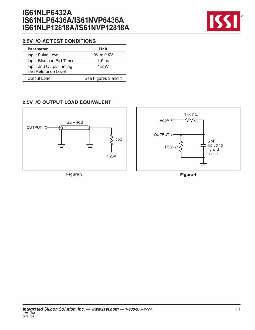
IS61NLP6432AIS61NLP6436A/IS61NVP6436AIS61NLP12818A/IS61NVP12818A2.5V I/O AC TEST CONDITIONS
Parameter Unit Input Pulse Level 0V to 2.5V Input Rise and Fall Times 1.5 ns Input and Output Timing 1.25V and Reference Level
Output Load See Figures 3 and 4
ZO = 50Ω
1.25V
50Ω
OUTPUT
1,667 Ω
5 pFIncludingjig andscope
1,538 Ω
OUTPUT
+2.5V
Figure 3 Figure 4
2.5V I/O OUTPUT LOAD EQUIVALENT

12 Integrated Silicon Solution, Inc. — www.issi.com — 1-800-379-4774Rev. 00A08/31/05
IS61NLP6432AIS61NLP6436A/IS61NVP6436AIS61NLP12818A/IS61NVP12818AREAD/WRITE CYCLE SWITCHING CHARACTERISTICS(1) (Over Operating Range)
-250 -200 Symbol Parameter Min. Max. Min. Max. Unit
fmax Clock Frequency — 250 — 200 MHz
tkc Cycle Time 4.0 — 5 — ns
tkh Clock High Time 1.7 — 2 — ns
tkl Clock Low Time 1.7 — 2 — ns
tkq Clock Access Time — 2.6 — 3.1 ns
tkqx(2) Clock High to Output Invalid 0.8 — 1.5 — ns
tkqlZ(2,3) Clock High to Output Low-Z 0.8 — 1 — ns
tkqhZ(2,3) Clock High to Output High-Z — 2.6 — 3.0 ns
toeq Output Enable to Output Valid — 2.8 — 3.1 ns
toelZ(2,3) Output Enable to Output Low-Z 0 — 0 — ns
toehZ(2,3) Output Disable to Output High-Z — 2.6 — 3.0 ns
tAs Address Setup Time 1.2 — 1.4 — ns
tws Read/Write Setup Time 1.2 — 1.4 — ns
tces Chip Enable Setup Time 1.2 — 1.4 — ns
tse Clock Enable Setup Time 1.2 — 1.4 — ns
tAdVs Address Advance Setup Time 1.2 — 1.4 — ns
tds Data Setup Time 1.2 — 1.4 — ns
tAh Address Hold Time 0.3 — 0.4 — ns
the Clock Enable Hold Time 0.3 — 0.4 — ns
twh Write Hold Time 0.3 — 0.4 — ns
tceh Chip Enable Hold Time 0.3 — 0.4 — ns
tAdVh Address Advance Hold Time 0.3 — 0.4 — ns
tdh Data Hold Time 0.3 — 0.4 — ns
tPds ZZ High to Power Down — 2 — 2 cyc
tPus ZZ Low to Power Down — 2 — 2 cycNotes:1. Configuration signal MODE is static and must not change during normal operation.2. Guaranteed but not 100% tested. This parameter is periodically sampled.3. Tested with load in Figure 2.

Integrated Silicon Solution, Inc. — www.issi.com — 1-800-379-4774 13Rev. 00A08/31/05
IS61NLP6432AIS61NLP6436A/IS61NVP6436AIS61NLP12818A/IS61NVP12818A
SLEEP MODE TIMING
SLEEP MODE ELECTRICAL CHARACTERISTICS
Symbol Parameter Conditions Min. Max. Unit
Isb2 Current during SLEEP MODE ZZ ≥ VIh 35 mA
tPds ZZ active to input ignored 2 cycle
tPus ZZ inactive to input sampled 2 cycle
tZZI ZZ active to SLEEP current 2 cycle
trZZI ZZ inactive to exit SLEEP current 0 ns
Don't Care
Deselect or Read Only Deselect or Read Only
tRZZI
CLK
ZZ
Isupply
All Inputs (except ZZ)
Outputs (Q)
ISB2
ZZ setup cycle ZZ recovery cycle
Normaloperation
cycle
tPDS tPUS
tZZI
High-Z

14 Integrated Silicon Solution, Inc. — www.issi.com — 1-800-379-4774Rev. 00A08/31/05
IS61NLP6432AIS61NLP6436A/IS61NVP6436AIS61NLP12818A/IS61NVP12818AREAD CYCLE TIMING
tDS
CLK
ADV
Address
WRITE
CKE
CE
OE
Data Out
A1 A2 A3
tKH tKL
tKC
Q3-3 Q3-4Q3-2Q3-1Q2-4Q2-3Q2-2Q2-1
Don't Care
Undefined
NOTES: WRITE = L means WE = L and BWx = L WE = L and BWX = L CE = L means CE1 = L, CE2 = H and CE2 = L CE = H means CE1 = H, or CE1 = L and CE2 = H, or CE1 = L and CE2 = L
tOEHZ
tSE tHE
tAS tAH
tWS tWH
tCES tCEH
tADVS tADVH
tKQHZtKQtOEQ tOEHZ
Q1-1

Integrated Silicon Solution, Inc. — www.issi.com — 1-800-379-4774 15Rev. 00A08/31/05
IS61NLP6432AIS61NLP6436A/IS61NVP6436AIS61NLP12818A/IS61NVP12818AWRITE CYCLE TIMING
tDS tDH
CLK
ADV
Address
WRITE
CKE
CE
OE
Data In
Data Out
A1 A2 A3
tKH tKL
tKC
tSE tHE
D3-3 D3-4D3-2D3-1D2-4D2-3D2-2D2-1D1-1
Don't Care
Undefined
NOTES: WRITE = L means WE = L and BWx = L WE = L and BWX = L CE = L means CE1 = L, CE2 = H and CE2 = L CE = H means CE1 = H, or CE1 = L and CE2 = H, or CE1 = L and CE2 = L
tOEHZ
Q0-3 Q0-4

16 Integrated Silicon Solution, Inc. — www.issi.com — 1-800-379-4774Rev. 00A08/31/05
IS61NLP6432AIS61NLP6436A/IS61NVP6436AIS61NLP12818A/IS61NVP12818ASINGLE READ/WRITE CYCLE TIMING
CLK
CKE
Address
WRITE
CE
ADV
OE
Data Out
Data In D5
tSE tHE
tKH tKL
tKC
Don't CareUndefined
NOTES: WRITE = L means WE = L and BWx = L CE = L means CE1 = L, CE2 = H and CE2 = L CE = H means CE1 = H, or CE1 = L and CE2 = H, or CE1 = L and CE2 = L
D2
tOELZ
tOEQ
A1 A2 A3 A4 A5 A6 A7 A8 A9
Q1 Q3 Q4 Q6 Q7
tDS tDH

Integrated Silicon Solution, Inc. — www.issi.com — 1-800-379-4774 17Rev. 00A08/31/05
IS61NLP6432AIS61NLP6436A/IS61NVP6436AIS61NLP12818A/IS61NVP12818ACKE OPERATION TIMING
A1 A2 A3 A4 A5 A6
Q1 Q3 Q4
CLK
CKE
Address
WRITE
CE
ADV
OE
Data Out
Data In D2
tSE tHE
tKH tKL
tKC
tKQLZ
tKQHZtKQ
tDHtDS
Don't CareUndefined
NOTES: WRITE = L means WE = L and BWx = L CE = L means CE1 = L, CE2 = H and CE2 = L CE = H means CE1 = H, or CE1 = L and CE2 = H, or CE1 = L and CE2 = L

18 Integrated Silicon Solution, Inc. — www.issi.com — 1-800-379-4774Rev. 00A08/31/05
IS61NLP6432AIS61NLP6436A/IS61NVP6436AIS61NLP12818A/IS61NVP12818ACE OPERATION TIMING
Don't CareUndefined
CLK
CKE
Address
WRITE
CE
ADV
OE
Data Out
Data In
tSE tHE
tKH tKL
tKC
NOTES: WRITE = L means WE = L and BWx = L CE = L means CE1 = L, CE2 = H and CE2 = L CE = H means CE1 = H, or CE1 = L and CE2 = H, or CE1 = L and CE2 = L
D5D3
tDHtDS
tOELZ
tOEQ
Q1 Q2 Q4
tKQHZ
tKQLZ
tKQ
A1 A2 A3 A4 A5

Integrated Silicon Solution, Inc. — www.issi.com — 1-800-379-4774 19Rev. 00A08/31/05
IS61NLP6432AIS61NLP6436A/IS61NVP6436AIS61NLP12818A/IS61NVP12818A
ORDERING INFORMATION (VDD = 3.3V/VDDq = 2.5V/3.3V)
Commercial Range: 0°C to +70°C Access Time Order Part Number Package
64Kx32
250 IS61NLP6432A-250TQ 100 TQFP
200 IS61NLP6432A-200TQ 100 TQFP
64Kx36
250 IS61NLP6436A-250TQ 100 TQFP
200 IS61NLP6436A-200TQ 100 TQFP
128Kx18
250 IS61NLP12818A-250TQ 100 TQFP
200 IS61NLP12818A-200TQ 100 TQFP
Industrial Range: -40°C to +85°C Access Time Order Part Number Package
64Kx32
250 IS61NLP6432A-250TQI 100 TQFP
200 IS61NLP6432A-200TQI 100 TQFP 200 IS61NLP6432A-200TQLI 100 TQFP, Lead-free
64Kx36
250 IS61NLP6436A-250TQI 100 TQFP
200 IS61NLP6436A-200TQI 100 TQFP
128Kx18
250 IS61NLP12818A-250TQI 100 TQFP
200 IS61NLP12818A-200TQI 100 TQFP 200 IS61NLP12818A-200TQLI 100 TQFP, Lead-free

20 Integrated Silicon Solution, Inc. — www.issi.com — 1-800-379-4774Rev. 00A08/31/05
IS61NLP6432AIS61NLP6436A/IS61NVP6436AIS61NLP12818A/IS61NVP12818AORDERING INFORMATION (VDD = 2.5V/VDDq = 2.5V)
Commercial Range: 0°C to +70°C Access Time Order Part Number Package
64Kx36
250 IS61NVP6436A-250TQ 100 TQFP
200 IS61NVP6436A-200TQ 100 TQFP
128Kx18
250 IS61NVP12818A-250TQ 100 TQFP
200 IS61NVP12818A-200TQ 100 TQFP
Industrial Range: -40°C to +85°C Access Time Order Part Number Package
64Kx36
250 IS61NVP6436A-250TQI 100 TQFP
200 IS61NVP6436A-200TQI 100 TQFP
128Kx18
250 IS61NVP12818A-250TQI 100 TQFP
200 IS61NVP12818A-200TQI 100 TQFP