is your bus arbiter really fair? restoring fairness in axi
TRANSCRIPT
Is Your Bus Arbiter Really Fair?Restoring Fairness in AXI Interconnects for FPGA SoCs
FRANCESCO RESTUCCIA, Scuola Superiore Sant’AnnaMARCO PAGANI, Scuola Superiore Sant’Anna and CRIStAL (Univ. Lille, CNRS, Centrale Lille, UMR 9189)ALESSANDRO BIONDI, Scuola Superiore Sant’AnnaMAURO MARINONI, Scuola Superiore Sant’AnnaGIORGIO BUTTAZZO, Scuola Superiore Sant’Anna
AMBA AXI is a popular bus protocol that is widely adopted as the medium to exchange data in field-programmable gate array system-on-chips (FPGA SoCs). The AXI protocol does not specify how conflictingtransactions are arbitrated and hence the design of bus arbiters is left to the vendors that adopt AXI. Typically,a round-robin arbitration is implemented to ensure a fair access to the bus by the master nodes, as for thepopular SoCs by Xilinx.
This paper addresses a critical issue that can arise when adopting the AXI protocol under round-robinarbitration; specifically, in the presence of bus transactions with heterogeneous burst sizes. First, it is shownthat a completely unfair bandwidth distribution can be achieved under some configurations, making possibleto arbitrarily decrease the bus bandwidth of a target master node. This issue poses serious performance, safety,and security concerns. Second, a low-latency (one clock cycle) module named AXI burst equalizer (ABE) isproposed to restore fairness. Our investigations and proposals are supported by implementations and testsupon three modern SoCs. Experimental results are reported to confirm the existence of the issue and assessthe effectiveness of the ABE with bus traffic generators and hardware accelerators from the Xilinx’s IP library.
CCS Concepts: • Computer systems organization→ Embedded and cyber-physical systems; • Hard-ware → Reconfigurable logic and FPGAs; Programmable interconnect; Safety critical systems;
Additional Key Words and Phrases: FPGA, AXI BUS, Arbitration, Embedded Systems
ACM Reference Format:Francesco Restuccia, Marco Pagani, Alessandro Biondi, Mauro Marinoni, and Giorgio Buttazzo. 2019. Is YourBus Arbiter Really Fair? Restoring Fairness in AXI Interconnects for FPGA SoCs. J. ACM 00, 0, Article 000( 2019), 22 pages. https://doi.org/xxx
This article appears as part of the ESWEEK-TECS special issue and was presented in the International Conference onCompilers, Architecture, and Synthesis for Embedded Systems (CASES) 2019
Authors’ addresses: Francesco Restuccia, [email protected], Scuola Superiore Sant’Anna, Pisa, Italy;Marco Pagani, [email protected], Scuola Superiore Sant’Anna, Pisa, Italy, CRIStAL (Univ. Lille, CNRS, CentraleLille, UMR 9189), Lille, France; Alessandro Biondi, [email protected], Scuola Superiore Sant’Anna, Pisa,Italy; Mauro Marinoni, [email protected], Scuola Superiore Sant’Anna, Pisa, Italy; Giorgio Buttazzo, [email protected], Scuola Superiore Sant’Anna, Pisa, Italy.
Permission to make digital or hard copies of all or part of this work for personal or classroom use is granted without feeprovided that copies are not made or distributed for profit or commercial advantage and that copies bear this notice andthe full citation on the first page. Copyrights for components of this work owned by others than ACM must be honored.Abstracting with credit is permitted. To copy otherwise, or republish, to post on servers or to redistribute to lists, requiresprior specific permission and/or a fee. Request permissions from [email protected].© 2019 Association for Computing Machinery.0004-5411/2019/0-ART000 $15.00https://doi.org/xxx
J. ACM, Vol. 00, No. 0, Article 000. Publication date: 2019.

000:2 Restuccia, et al.
1 INTRODUCTIONThe AMBA AXI bus protocol was proposed by ARM more than 15 years ago as an evolution ofprevious solutions (such as AMBA APB and AMBA AHB) for internal connections in System-on-Chips (SoCs). Since then, the protocol has been widely adopted due to a number of advantages, suchas being an open standard that is fully compatible with the popular ARM Cortex processors. Therange of platforms that rely on AMBA AXI has grown, reaching devices with a level of complexityand flexibility way beyond those of the initial chips targeted by the protocol. A relevant case is theone of SoCs equipped with field-programmable gate arrays (FPGA) where the programmable logic(PL) communicates with the memory controller through the AMBA AXI protocol. AXI will be evenadopted in the upcoming new-generation platforms by Xilinx that rely on a network-on-chip withAXI-based links [25].
FPGA SoCs are promising computing platforms to manage the increasing software complexityand computational demand of modern embedded systems. In particular, they are particularlyattractive as they allow deploying high-performance, yet energy-efficient hardware acceleratorsonto the FPGA fabric, while making use of the plethora of pure software solutions (such as Linux,communication stacks, drivers, etc.) that can be executed upon the multicore processor(s) availablein the SoC.In these platforms, it is possible to deploy very different kinds of hardware modules, even
dynamically programmed at run-time, which act as masters on the bus and are allowed to issuebus transactions with different structures. During the last decade, component-based design forapplications that make use of FPGAs has been more and more adopted, as it allows designersto build systems by combining Intellectual Properties blocks (IPs) developed by different teamsor even different companies. This trend has been accelerated with the development of advancedhigh-level synthesis (HLS) tools [12]. For instance, some companies sell proprietary IP libraries,which are usually distributed in a closed-source form that forbids the designers working at theintegration level to view or edit their behavioral functional description.
Furthermore, it is also common that closed-source IPs do not allow controlling the way they issuebus transactions. This limitation becomes particularly relevant for the case of hardware accelerators,which are typically memory-intensive as they commonly work on large amount of data, and hencegenerate a consistent traffic on the bus. Indeed, the way bus transactions for memory access aremanaged in the SoC is crucial for the system performance [13, 27], especially when time-sensitivesystems are designed.
Nevertheless, the AXI protocol leaves flexibility on the way bus transactions are structured, whilenot mandating specific arbitration policies, hence leaving the burden of designing bus arbitersto the vendors that adopt AXI. To ensure a fair redistribution of the bus bandwidth, the mostcommon solution consists in adopting the round-robin arbitration policy, as for the popular SoCsby Xilinx (e.g., those belonging to the Zynq-7000 and Zynq-Ultrascale families). Despite the use of around-robin arbitration results in a simple and effective solution, we found that its integration withthe AXI protocol may lead to critical issues under specific configurations of the bus transactions.
Contributions. This paper first shows that the integration of the round-robin policy with the AXIprotocol may lead to a completely unfair bandwidth distribution in the presence of bus transactionswith heterogeneous burst sizes. Just to mention a representative result, in a scenario with threehardware accelerator IPs it is possible to reduce the memory bandwidth of a victim IP of about91%, with respect to the expected bandwidth (i.e., the one assigned by a fair arbitration). In otherscenarios, it is even possible to reach larger bandwidth reductions, bringing the available bandwidthof the victim IP arbitrarily close to 0%, thus completely jeopardizing its functionality.
J. ACM, Vol. 00, No. 0, Article 000. Publication date: 2019.

Is Your Bus Arbiter Really Fair?Restoring Fairness in AXI Interconnects for FPGA SoCs 000:3
The problem is shown to be originated by the structure of the memory transactions generatedby each IP—hence, by a local property of each IP— and poses serious risks for at least two reasons.First, when applying component-based design, where IPs from different vendors or developedby different teams are integrated, this issue can be triggered any time when the structure of thememory transactions of each IP cannot be controlled at the stage of integration, e.g., in the presenceof proprietary IPs. The presence of IPs with different burst sizes is a very plausible scenario, as thestructure of memory transactions can even be controlled from high-level synthesis (HLS) by meansof specific pragma statements. Second, since modern FPGAs offer dynamic partial reconfiguration(DPR) capabilities, which allows reprogramming a portion of the FPGA area while the system isoperating, the system can be exposed to performance/safety/security issues if malicious IPs aredynamically configured to generate crafted bus transactions, e.g., to realize a denial-of-serviceattack.A practical solution consisting in a low-latency (one extra clock cycle) IP named AXI burst
equalizer (ABE) is proposed to restore fairness. The ABE mediates the bus traffic generated by IPs by(i) splitting outgoing address requests to an equalized (i.e., nominal) burst size, (ii) merging/splittingincoming data, and (iii) equalizing the number of outstanding transactions. The ABE has beenevaluated upon three modern FPGA-based SoCs (two of the Zynq-7000 family and one fromthe Zynq-Ultrascale family by Xilinx) by means of benchmarks and case studies, demonstratingits ability to restore a fair bandwidth distribution in accessing the memory bus. Despite theexperimental results reported in the paper focus on Xilinx FPGA SoCS, the ABE also applies toother products that adopt AXI and rely on round-robin bus arbitration.
2 ESSENTIAL BACKGROUNDA typical FPGA SoC architecture combines a processing system (PS) (generally based on one ormore processors) with a Field Programmable Gate Array (FPGA) subsystem in a single device.Both the subsystems access a DRAM controller through which they can access a shared DRAMmemory. Figure 1 illustrates a typical SoC FPGA architecture in which two interfaces allow thecommunication between the FPGA subsystem and the processing system (PS). The de-facto standardinterface for interconnections is the ARM Advanced Microcontroller Bus Architecture AdvancedeXtensible Interface (AMBA AXI) [1].
DRAMController
FPGA-PS Interface
PS Interconnect
APU
ARM CoresARM Cores
I/O peripherals
Custom logic
FPGA PS
PS-FPGA Interface
Fig. 1. Simplified architecture of a SoC FPGA platform.
The AXI bus. The AMBA AXI standard defines a master-slave interface to allow simultaneousbi-directional data exchange. An AXI port interface is composed of five independent channels:Address Read (AR channel), Address Write (AW channel), Data Read (R channel), Data Write (Wchannel), and Write Response (B channel). Each channel is composed by a standard-defined setof signals. In an AXI-based interconnection, all the transactions are started by a master, whichrequests to read/write data from/to a slave interface through AR or AW channels, respectively. Data
J. ACM, Vol. 00, No. 0, Article 000. Publication date: 2019.

000:4 Restuccia, et al.
reads are routed back to the requesting device through R channels, while data writes are routed tothe correct destination through W channels. The B channel is used by the destination device of awrite request to acknowledge the master that its request has been correctly served. Each of thefive AXI channels implements a handshake mechanism based on two signals: the ready signal andthe valid signal. Depending on the channel type, one signal is controlled by the master interface,while the corresponding slave interface controls the other. When both signals are high, the requestor the data are transmitted. The AXI standard allows masters to issue multiple pending requests.This means that, in principle, each master is allowed to issue an unlimited number of outstandingtransactions. Typically, the number of outstanding transactions is limited by the designer of the IP.Following data requests on the AR and AW channels, data are transmitted back to the master onthe R channel (for read data) or provided to the W channel (for write data) in the same order asrequests have been routed to the corresponding address channel. This means that data channelsare completely dependent on address channels, that is, the access to the output data channels R andW depends on the order in which requests are routed to the address channels. This feature is reportedin the documentation of many commercial devices [18, 19] and has been experimentally validatedfor the platforms analyzed in this paper (see Section 5).
AXI ports. As it is illustrated in Figure 1, the communication between the FPGA and the PS isallowed by two different types of interfaces: the PS-FPGA interface and the FPGA-PS interface. Thefirst one offers a slave interface to the FPGA and is used by the processors to control the hardwaredevices or access data in the FPGA. In a dual manner, the second one offers a slave interface to thePS and is used by modules deployed on the FPGA (e.g., hardware accelerators) to access the centralDRAM memory or the on-chip memory in the PS. In the considered architecture, the slave portinterface on the PS side (FPGA-PS interface) is split into different ports. Each of such ports allowsaccessing a single, but configurable range of contiguous addresses in the PS. Note that, when tworequests refer to disjoint address ranges mapped to different ports, no bus arbitration is required,as they can be served in parallel.
AXI Interconnects.Whenever multiple AXI masters want to access the same output port, an AXIInterconnect is in charge of arbitrating conflicting requests to the same port. The access to eachchannel of the output AXI port is managed by a multiplexer. Each multiplexer is controlled by anarbiter, which decides at each time which input port is granted to the output channel. The arbitersare completely independent from each other.
For instance, in FPGA SoCs by Xilinx, two implementations of the Interconnect are available: AXIInterconnect (deprecated in the latest platforms) and AXI SmartConnect. Both the implementationsare multiplexer-based and therefore comply with the structure described above.
Arbitration policy. In this work, each arbiter is assumed to implement a round-robin policy, whichto the best of our records is the most common solution in off-the-shelf platforms. For instance, theAXI arbiters for FPGA SoCs by Xilinx implement round-robin (both the AXI Interconnect and theAXI SmartConnect, see [20, 24]). Round-robin arbitration should guarantee fairness in contendingthe bus; specifically, it should guarantee a fair distribution of the bus bandwidth among the IPsthat contend a port.
Burst sizes. AXI offers two methods for transmitting data between masters and slaves: singletransactions or transaction bursts. When operating in burst mode, the requesting device can issuea single address request to fetch/write up to 256 data words per request. Typically, hardwareaccelerators work on large amount of data. Therefore, burst transactions are preferable than singletransactions to avoid issuing a large number of addresses, hence reducing the overhead of thehardware accelerator related to its addressing phases.
J. ACM, Vol. 00, No. 0, Article 000. Publication date: 2019.
Is Your Bus Arbiter Really Fair?Restoring Fairness in AXI Interconnects for FPGA SoCs 000:5
AXI allows for bursts of different sizes. The burst size is a property of each IP configured by thedeveloper. Burst sizes may also be implicitly set to default values when using libraries or high-levelsynthesis (HLS), with the result that designers may be unaware of the burst size adopted by their IP.The configuration of burst sizes is also exposed to HLS with specific pragma statements. In general,when developing IPs in HDL, the developer has a lot of freedom in configuring the burst sizes, whichmay even change at run-time. Overall, when deploying multiple IPs on the same FPGA, possiblydeveloped by different teams or even different companies, it is likely to have multiple masterson the bus that issue transactions with heterogeneous burst sizes. Furthermore, when integratingcommercial closed-source IPs, it may not even be possible to configure their burst sizes.
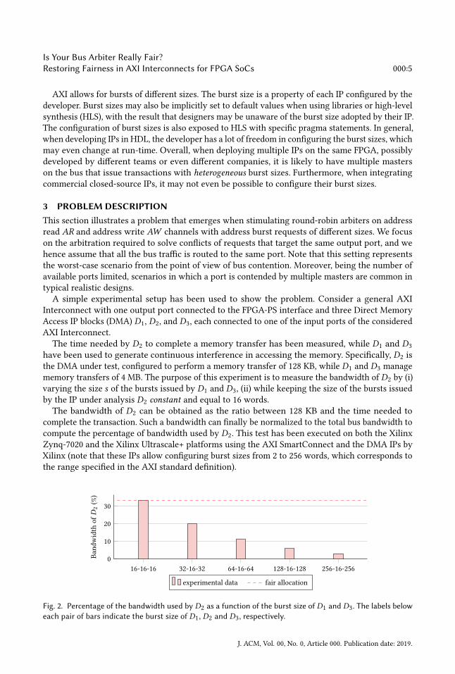
3 PROBLEM DESCRIPTIONThis section illustrates a problem that emerges when stimulating round-robin arbiters on addressread AR and address write AW channels with address burst requests of different sizes. We focuson the arbitration required to solve conflicts of requests that target the same output port, and wehence assume that all the bus traffic is routed to the same port. Note that this setting representsthe worst-case scenario from the point of view of bus contention. Moreover, being the number ofavailable ports limited, scenarios in which a port is contended by multiple masters are common intypical realistic designs.A simple experimental setup has been used to show the problem. Consider a general AXI
Interconnect with one output port connected to the FPGA-PS interface and three Direct MemoryAccess IP blocks (DMA) D1, D2, and D3, each connected to one of the input ports of the consideredAXI Interconnect.
The time needed by D2 to complete a memory transfer has been measured, while D1 and D3have been used to generate continuous interference in accessing the memory. Specifically, D2 isthe DMA under test, configured to perform a memory transfer of 128 KB, while D1 and D3 managememory transfers of 4 MB. The purpose of this experiment is to measure the bandwidth of D2 by (i)varying the size s of the bursts issued by D1 and D3, (ii) while keeping the size of the bursts issuedby the IP under analysis D2 constant and equal to 16 words.The bandwidth of D2 can be obtained as the ratio between 128 KB and the time needed to
complete the transaction. Such a bandwidth can finally be normalized to the total bus bandwidth tocompute the percentage of bandwidth used by D2. This test has been executed on both the XilinxZynq-7020 and the Xilinx Ultrascale+ platforms using the AXI SmartConnect and the DMA IPs byXilinx (note that these IPs allow configuring burst sizes from 2 to 256 words, which corresponds tothe range specified in the AXI standard definition).
16-16-16 32-16-32 64-16-64 128-16-128 256-16-2560
10
20
30
Band
width
ofD2(%)
experimental data fair allocation
Fig. 2. Percentage of the bandwidth used by D2 as a function of the burst size of D1 and D3. The labels beloweach pair of bars indicate the burst size of D1, D2 and D3, respectively.
J. ACM, Vol. 00, No. 0, Article 000. Publication date: 2019.

000:6 Restuccia, et al.
The red bars in Figure 2 report the results of the experiment for s ∈ {16,32,64,128,256}. Ideally,the round-robin arbitration should guarantee a fair redistribution of the available bandwidth,reserving one third of the total bandwidth (about 33%) to each DMA. However, as clear fromFigure 2, this is the case only when all the three DMAs issue transactions with the same burstsize. The results also show that the bandwidth of D2 significantly decreases as the burst size of theother DMAs increases, reaching about the 3% of the total bandwidth for s = 256. Note that thelatter case corresponds to just the 9% of the expected bandwidth, which means a 91% drop withrespect of the expected bandwidth! To make things worse, a larger bandwidth reduction can beobtained by increasing the number of interfering DMAs, reaching configurations in which theexecution of a DMA is completely jeopardized (further details will be provided in Section 5). Fromthis experiment, it is possible to conclude that the integration of round-robin arbitration with the AXIprotocol can cause an unfair distribution of the bandwidth in the presence of heterogeneous burst sizes.As mentioned in the introduction, this issue may be critical when integrating multiple IPs developedby independent teams (possibly with closed-source, and hence unknown non-configurable burstsizes), or in the presence of systems in which part of the FPGA could be reconfigured to maliciouslyintroduce “bandwidth-stealing” modules.
3.1 In-depth analysisThis section aims at analyzing in details the problem presented above. To this end, consider thedesign illustrated in Figure 3. The design is composed of three hardware accelerators (HWA1, HWA2,and HWA3) that issue burst transactions (reads or writes) to the central memory controller (DRAMCTRL) located in the PS, while the AXI Interconnect arbitrates the address burst requests to accessthe OUT slave port interface in the FPGA-PS interface. HWA2 issues burst transactions with a lengthof S words. Differently, HWA1 and HWA3 issue burst transactions with size 2S . For instance, HWA1 canbe a typical hardware task synthesized with HLS, while HWA2, and HWA3 can be two DMAs.
M
M
M
S
S
S
S
AXIInterconnect
M
ProcessingSystem
DRAMCtrl.
OUT2
3
AXI bus
12S
HWA1
HWA2
HWA32S
S
Fig. 3. Sample architecture to probe the bandwidth allocation in the presence of heterogeneous burst sizetransactions.
Consider the case in which the three hardware accelerators simultaneously issue a read requeston the corresponding AXI Address Read channelAR1,AR2, andAR3, respectively (the same examplecan be extended to write channels). Also, to cope with the worst-case scenario, it is assumed thatthe corresponding hardware accelerators can provide a new request immediately after the AXIInterconnect granted a request and presented it to the slave OUT Port Address Channel in theFPGA-PS interface (named AROUT ).Figure 4 reports a simplified waveform diagram re-created by observing real traces on a Xilinx
Zynq SoC platform (a bus signal analysis has been performed upon three state-of-the-art platforms,namely the Zynq Z-7010, Zynq Z-7020, and the Zynq Ultrascale+ ZU9EG, obtaining the sameresults). The corresponding design has been developed with Xilinx Vivado 2018.2, making use ofthe state-of-the-art Xilinx IPs.
J. ACM, Vol. 00, No. 0, Article 000. Publication date: 2019.

Is Your Bus Arbiter Really Fair?Restoring Fairness in AXI Interconnects for FPGA SoCs 000:7
S S S S S
2S 2S 2S 2S 2SAR1
AR2
AR3
AROUT
R1
R2
R3
ROUT
2S S 2S 2S S 2S 2S S 2S 2S S
2S 2S 2S 2S
S
CLK
S
S
S S S S
S
S
S
S S
NO DATA
2S
S
Req burst size 2S
Req burst size S
S S data back
Request accepted, preparing new one
Waiting to be accepted
Changing data
t0 t1 t2 t3 t4 t5 t6 t7 t8 t9 t10
AR Round Robin Cycle Equivalent R Round Robin Cycle
Time
Fig. 4. Simplified waveform of the arbitration for the sample architecture of Figure 3.
The diagram illustrates the input address requests and the corresponding outputs in accordanceto the round-robin arbitration policy. To simplify the presentation and focus on relevant aspects,it is assumed that (i) the PS is always ready to accept address requests from the AXI slave portunder analysis in the FPGA-PS interface (i.e., the one related to the OUT port); and (ii) the readchannels (i.e., ROUT , R1, R2, and R3 in the figure) have a width of S words each, so that S words canbe transferred in one clock cycle.
As it can be noted from the diagram, at time t1, each of the three hardware accelerators providesits first burst request (i.e., AR1, AR2, and AR3). At time t2, the round-robin arbiter on AR channeldecides to accept the request coming from HWA1 and routes it through the AR channel of the OUTport. After the request is sampled, a new one is provided by HWA1 on AR1. Analogously, the requestcoming from HWA2 is admitted at time t3, while the one coming from HWA3 is granted at time t4. Thiscompletes the round-robin period of the input AR channels (each hardware accelerator has routeda request to the output). Hence, at time t5, a new request can be accepted from HWA1.
At time t6, the first chunk of data is provided from memory on the common read channel ROUT .Since the address requests are served in order, this data is related to the first request acceptedfrom HWA1; thus, the chunk is routed to HWA1 through its read channel R1. The second chunk ofdata coming from memory at time t7 is still related to HWA1, so it is also routed to R1. The samehappens at time t8 for the data requested by HWA2 (single chunk), and at times t9 and t10 for the datarequested by HWA3 (two chunks).
The diagram reported in Figure 4, and in particular the timelines of channels ROUT , R1, R2, andR3, allow us to clearly identify the cause of the problem presented in the previous section. Despitethe requests on the address channel AROUT are accepted in round-robin order, their correspondingdata transfers to the hardware accelerators do not respect a perfectly-balanced round-robin order(see the ROUT channel)—that is, the round-robin arbitration is preserved on address channels, but withdifferent per-master granularity, which depends on the burst sizes. Indeed, as data must be transmitted
J. ACM, Vol. 00, No. 0, Article 000. Publication date: 2019.
000:8 Restuccia, et al.
in accordance to the order with which the address requests are granted, they cannot be providedon channels R1, R2, and R3 in a fair manner, i.e., with the granularity of S words per hardwareaccelerator.
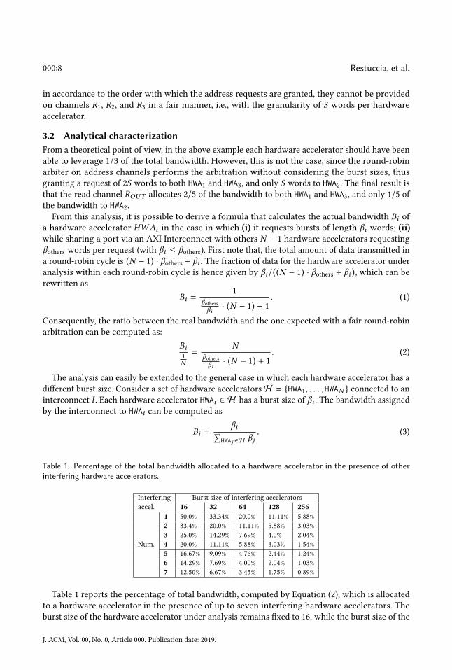
3.2 Analytical characterizationFrom a theoretical point of view, in the above example each hardware accelerator should have beenable to leverage 1/3 of the total bandwidth. However, this is not the case, since the round-robinarbiter on address channels performs the arbitration without considering the burst sizes, thusgranting a request of 2S words to both HWA1 and HWA3, and only S words to HWA2. The final result isthat the read channel ROUT allocates 2/5 of the bandwidth to both HWA1 and HWA3, and only 1/5 ofthe bandwidth to HWA2.From this analysis, it is possible to derive a formula that calculates the actual bandwidth Bi of
a hardware accelerator HWAi in the case in which (i) it requests bursts of length βi words; (ii)while sharing a port via an AXI Interconnect with others N − 1 hardware accelerators requestingβothers words per request (with βi ≤ βothers). First note that, the total amount of data transmitted ina round-robin cycle is (N − 1) · βothers + βi . The fraction of data for the hardware accelerator underanalysis within each round-robin cycle is hence given by βi/((N − 1) · βothers + βi ), which can berewritten as
Bi =1
βothersβi· (N − 1) + 1
. (1)
Consequently, the ratio between the real bandwidth and the one expected with a fair round-robinarbitration can be computed as:
Bi1N
=N
βothersβi· (N − 1) + 1
. (2)
The analysis can easily be extended to the general case in which each hardware accelerator has adifferent burst size. Consider a set of hardware acceleratorsH = {HWA1, . . . ,HWAN } connected to aninterconnect I . Each hardware accelerator HWAi ∈ H has a burst size of βi . The bandwidth assignedby the interconnect to HWAi can be computed as
Bi =βi∑
HWAj ∈H βj. (3)
Table 1. Percentage of the total bandwidth allocated to a hardware accelerator in the presence of otherinterfering hardware accelerators.
Interferingaccel.
Burst size of interfering accelerators16 32 64 128 256
Num.
1 50.0% 33.34% 20.0% 11.11% 5.88%2 33.4% 20.0% 11.11% 5.88% 3.03%3 25.0% 14.29% 7.69% 4.0% 2.04%4 20.0% 11.11% 5.88% 3.03% 1.54%5 16.67% 9.09% 4.76% 2.44% 1.24%6 14.29% 7.69% 4.00% 2.04% 1.03%7 12.50% 6.67% 3.45% 1.75% 0.89%
Table 1 reports the percentage of total bandwidth, computed by Equation (2), which is allocatedto a hardware accelerator in the presence of up to seven interfering hardware accelerators. Theburst size of the hardware accelerator under analysis remains fixed to 16, while the burst size of the
J. ACM, Vol. 00, No. 0, Article 000. Publication date: 2019.

Is Your Bus Arbiter Really Fair?Restoring Fairness in AXI Interconnects for FPGA SoCs 000:9
interfering hardware accelerators is the same and varies from 16 to 256. As it can be noted fromthe table, in the presence of seven interfering hardware accelerators with burst size equal to 256,the bandwidth of the victim IP can be reduced to the 0.89% of the total bus bandwidth!
4 PROPOSED SOLUTIONThis work addresses the issue presented in the previous section by proposing a practical solutionthat consists of an IP named AXI Burst Equalizer (ABE). The ABE is conceived to be placed betweeneach hardware accelerator and an input port of an AXI Interconnect and serves the purpose ofequalizing the address burst requests issued by the hardware accelerator. The main objective of theABE is to achieve a fair bus bandwidth allocation in the presence of round-robin arbitration. Thisfeature is particularly useful when hardware accelerators are subject to worst-case timing analysis,e.g., in the case they are part of a real-time system [3].The ABE preserves standard interconnections by employing two AXI ports: the master port of
the hardware accelerator connects to a slave port of the ABE, while the slave input port of the AXIInterconnect connects to a master port in the ABE, as illustrated in Figure 5. The ABE implementsthe standard AXI handshaking mechanism and supports any permissible burst size.
M
M
M
S
S
S
S
AXIInterconnect
M
ProcessingSystem
DRAMCTRL
OUT2
3
AXI bus1
2SHWA1
SHWA2
2SHWA3
S MABE1
S MABE2
S MABE3
Eq1
Eq2
Eq3
Fig. 5. Extension of the sample architecture to include the ABEs.
An ABE is characterized by two configuration parameters, i.e., (i) a nominal burst size β̂ , and (ii)a maximum number L̂ of outstanding transactions, and complies with the following rules:R1 In accordance to the AXI standard, each hardware accelerator can initiate a transaction by
issuing to its corresponding ABE two types of requests: (i) address read requests, denoted byRR , with burst size βR ; and (ii) address write requests, denoted by RW , with burst size βW .
R2 If βR ≤ β̂ (or βW ≤ β̂ for write requests), the ABE forwards the request issued by the correspond-ing hardware accelerator to the AXI Interconnect without any modification. Otherwise, whenβR > β̂ (or βW > β̂), request RR (or RW ) is split into C =
⌈βR/β̂
⌉sub-requests RR1 ,RR2 ,...,RRC
(or C =⌈βW /β̂
⌉sub-requests RW1 ,RW2 ,...,RWC ) that have at most the nominal burst size β̂ .
R3 The ABE sequentially propagates the sub-requests mentioned in the previous rule to the AXIInterconnect.
R4 When an address read request RR is split into the RR1 ,RR2 ,...,RRC sub-requests, the ABE reassem-bles the corresponding incoming data chunks DR1 ,DR2 ,...,DRC into a single data response DRthat is compliant (according to the AXI standard) with the original request RR .
R5 When an address write request RW is split into the RW1 ,RW2 ,...,RWC sub-requests, the ABE alsosplits the corresponding outgoing write data DW intoC outgoing data chunks DW1 ,DW2 ,...,DWC .The corresponding write responses KW1 ,KW2 ,...,KWC on the B channel are merged into a singlewrite response KW .
R6 The ABE can issue at most L̂ nominal outstanding read transactions and L̂ nominal outstandingwrite transactions. Once the limit of outstanding transactions has been reached, the ABE must
J. ACM, Vol. 00, No. 0, Article 000. Publication date: 2019.

000:10 Restuccia, et al.
wait for the completion of a pending transaction before issuing a new transaction to the AXIInterconnect.
An implementation of the ABE has been realized in VHDL language and exported as an IP-XACTstandard package. It can be integrated on any platform compatible with the IP-XACT standard,as well as easily ported and packaged to other platforms that are not compatible with the IP-XACT standard. The internal hardware architecture of the ABE is presented in Appendix 4.5. Ourimplementation leverages cycle-level parallelism to minimize the latency introduced when splittingtransactions: further details are provided in Section 4.2. The reason for which the ABE limits thenumber of outstanding transactions (rule R6) is explained in Section 4.3.
4.1 Example: the ABE in actionLet us now consider the same example introduced in Section 3 and analyze the differences in thebus signals when the ABEs are installed (the same example can be extended to the case of writetransactions). As in Section 3, HWA2 issues address burst requests S words long, while HWA1 andHWA3 issue address burst requests 2S words long. The equalized channels mediated by the ABEs aredenoted with the subscripts eq1, eq2 and eq3. The nominal burst size β̂ is set to S . The (simplified)bus signals in the presence of ABEs are illustrated in Figure 6 (this figure has also been createdby observing real execution traces obtained from the same platforms considered in the previoussection).
S S S
2S 2S 2SAR1
AR2
AR3
AROUT
R1
R2
R3
ROUT
S S S S S S S S S S S
2S 2S 2S
S
CLK
S
S S S S S
S
S
S
S
S
S S
NO DATA
2S
S
Req burst size 2S
Req burst size S
S S data back
Request accepted, preparing new req
Waiting to be accepted
Changing data
S S S
S S SAReq1
AReq2
AReq3 S S S
S
S
S
S
S S S
2S
2S
AR Round Robin Cycle Equivalent R Round Robin Cycle
t0 t1 t2 t3 t4 t5 t6 t7 t8 t9 Time
Fig. 6. Waveform of an arbitration sequence in the presence of ABEs.
Each hardware accelerator issues a burst request at time t0 on the respective address read channel(AR1, AR2, and AR3) to be routed to the PS through the OUT port in the FPGA-PS interface. At
J. ACM, Vol. 00, No. 0, Article 000. Publication date: 2019.

Is Your Bus Arbiter Really Fair?Restoring Fairness in AXI Interconnects for FPGA SoCs 000:11
time t1, the ABEs (ABE1, ABE2, and ABE3) latch the address requests coming from the respectivehardware accelerators, thus releasing the buses (AR1, AR2 and AR3) and allowing the hardwareaccelerators to provide a new burst request. Since the size of the burst request coming from HWA2 isthe same of the nominal one, this request is directly routed to the output AReq2 channel withoutmodifications (rule R2). Conversely, since HWA1 and HWA3 provide requests of size 2S , ABE1 andABE3 issue to AReq1 and AReq3, respectively, partial burst requests with length S words (rule R2).
At time t2, the AXI Interconnect has in input three bursts requests of S words from ABE1, ABE2and ABE3. Let us suppose that the first granted request is the one on AReq1. Hence, the first partialburst request coming from HWA1 is granted and immediately latched on the AROUT channel attime t3. At the same time, ABE1 generates the next partial burst request, which completes theoriginal data request of size 2S and will become available on the AReq1 channel at time t3. Next,at time t4, the request on AReq2 is granted to the output port by the round-robin arbiter. Sinceit has the nominal burst size, it can be routed as it is by ABE2. After that, a new nominal burstrequest on the AR2 channel is provided to the AReq2 channel by ABE2. Then, similarly as forthe request generated by HWA1, the first chunk of the request issued by HWA3 is granted andlatched on the AROUT channel at time t5: this concludes the first round-robin cycle. The samearbitration scheme is repeated until the addressing phases are completed. As the requests have beengranted by following a round-robin arbitration scheme with a fair burst granularity of S words, thecorresponding data are also transmitted back on the R1, R2, and R3 channels with a granularity of Swords (see Fig. 6 from time t6 on). This allows achieving a fair bandwidth redistribution for thebus, with a consequent impact on the response times of the hardware accelerators — please refer toAppendix 4.4 for further details.
4.2 Extra latency introduced by the ABEImplementing the ABE in a HDL language allowed achieving high performance and optimizingits area consumption. The ABE has been designed to leverage the parallelism offered by the AXIprotocol to introduce as less latency as possible. It analyzes AXI channels in parallel by defininga specific VHDL process for each channel. Note that, as the ABE has to analyze the request fortransactions to identify their burst size, at least one cycle of latency is required to process therequest. Our implementation is able to perform the analysis of requests in the minimum time (onecycle). Conversely, when managing the data channels, our implementation does not introduceadditional latency as (i) it directly connects the upstream and downstream data channels; and (ii)monitors the data traffic to proactively perform splitting and merging tasks. Specifically, knowingthe nominal burst size of transactions, the ABE counts the number of words transmitted on datachannels and can hence be prepared to either split (by inserting the AXI-standard LAST signal onthe W channel) or merge (by removing LAST signals on the R channel) transactions one clock cyclein advance.
Figure 7 reports three examples to illustrate the latency introduced by the ABE: the first two arerelated to transactions issued without the ABE, and are used to explain the third example that refersto the case in which the ABE is present. To simplify the figure, only 8-word write transactions areconsidered (the same examples can be extended to other sizes and read transactions).First of all, note that a 8-word write data request can be served via either (i) a single burst
transaction with size 8 words; or (ii) with eight one-word long transactions. These two options areillustrated by Case 1 and Case 2 in Figure 7, respectively. The bus traffic on both the address (AW)and data (W) channels is considered.
Case 1. In this case, a 8-word burst is issued by a hardware accelerator to the memory controller.At time t1, the address burst request is accepted on the AW channel; hence, at the next clock cycle,the hardware accelerator can start providing data on theW channel (time t2). Assuming (to simplify
J. ACM, Vol. 00, No. 0, Article 000. Publication date: 2019.

000:12 Restuccia, et al.
CLK
8W
W W W W
W
W W W W
W W W
8W
W W W W
W W W W
AW
W
AW
AW
W
W
AWABE
Extra latency introduced by ABE
NO DATA
8W
W
Burst Req of 8 Words
Single Req one wordW Word of Data
Changing data
W W W W
W W W W
W W W W
W W W W
W W W W
Case 1
Case 2
Case 3
t0 t1 t2 t3 t5t4 Time
Fig. 7. Latency introduced by ABE to serve an 8-word write transaction.
the example) that the output port is always ready to accept data on the W channel, at time t4 allthe eight words have been transferred.
Case 2. In this case, the hardware accelerator still wants to transfer eight words of data, butissuing eight single-word transactions. According to the AXI standard, each word of data on the Wchannel has to be preceded by the corresponding address request on the AW channel. At time t1, thefirst address request is accepted on the AW channel. Assuming that the output port is always readyto accept data from the W channel, the hardware accelerator provides the first word of data at thenext clock cycle (time t2). Thanks to the parallelism of AXI (i.e., the presence of multiple channels),in the same clock cycle the hardware accelerator can provide a new address request for the nextword of data on the AW channel, while also transmitting data on the W channel. Consequently, theeight transactions complete in the same amount of clock cycles needed in Case 1.
Case 3. Here, the ABE is installed to mediate the traffic issued by the hardware acceleratorunder analysis. The ABE is configured with a nominal burst size of length one word. As in Case 1,the hardware accelerator issues a 8-word address burst request to the ABE on the AW channel attime t1. The ABE receives the request and, in one clock cycle, is able to provide the first nominaladdress burst request to the AWABE channel at time t2. This extra clock cycle corresponds to theonly latency introduced by the ABE. Indeed, at time t3, the hardware accelerator can issue thefirst word of data in the data channel W (corresponding to the first nominal burst) and, since datachannels are not decoupled by ABE, data are accepted directly at the output port without any otherlatency. At the same clock cycle, the ABE is ready to provide the next nominal address burst requeston the AWABE channel, and so on until the data transfer is completed. The transaction completesat time t5, which is just one clock cycle after the completion of the transaction(s) in Cases 1 and 2.This single-cycle latency is originated by a stage of the ABE that computes (and provides to theoutput port) the next nominal address burst request. Note that this latency is not affected by thesize of the nominal burst, nor by the size of the address burst requests in input to the ABE.
J. ACM, Vol. 00, No. 0, Article 000. Publication date: 2019.

Is Your Bus Arbiter Really Fair?Restoring Fairness in AXI Interconnects for FPGA SoCs 000:13
4.3 Limiting the number of outstanding transactionsAs discussed in Section 2, the AXI standard supports multiple outstanding transactions by allowingAXI masters modules to issue multiple reads or write address burst requests without waiting fortheir corresponding completions. The AXI standard itself does not impose any limit on themaximumnumber of outstanding transactions; however, in practical implementations of IPs, a maximumnumber of outstanding transactions is typically configured. In general, the number of maximumoutstanding transactions depends on the specific IP implementation. Once a master module hasreached the maximum number of outstanding transactions, it must wait for the completion of onepending transaction before issuing a new transaction. This practical limitation may be anothercause of unfair bandwidth allocation.For instance, consider two hardware accelerators connected to the same Interconnect: HWA1
issuing 16-word burst transactions and HWA2 issuing 64-word burst transactions. Assume that themaximum number of outstanding transactions is set to 2 for both hardware accelerators. Despite thenumber of outstanding transactions is the same, the ones issued by HWA2 request four times moredata than the ones issued by HWA1. This means that HWA2 can issue four times more outstandingdata than HWA1. Note that the same would occur in the presence of ABEs without rule R6.
Now, consider the case in which ABE modules, configured with nominal burst sizes of 16 words,are placed between each hardware accelerator and the Interconnect. In this scenario, the ABE willfragment each 64-word address burst request issued by HWA2 into 4 ones, each consisting of 16-wordbursts. However, from the perspective of HWA2, only a single transaction has been issued. Therefore,the ABE protecting HWA2 could potentially issue 4 · 2 = 8 outstanding 16-word transactions beforereaching its original limit (i.e., 2 outstanding 64-word transaction), while HWA1 can issue only two16-word outstanding transactions. This difference may lead to an unfair bus bandwidth allocation,as it is illustrated in the (simplified) waveform diagram reported in Figure 8.At time t0, both HWA1 and HWA2 prepare their first address requests. One cycle later, the ABEs
propagate the address requests to their corresponding AReq channels. The first arbitration cyclestarts at time t1 and ends at t2. The Interconnect arbitrates the first 4 address requests in a fair wayup to time t3, at which all address requests issued by HWA1 have been served. At this time, havingalready reached the limit of 2 outstanding transactions, HWA1 cannot issue further transactions.From this point on, all address requests from HWA2 are propagated without suffering contentionup to time t4, when HWA1 receives back the data corresponding to its first address request and canfinally issue a new transaction. In this scenario, HWA1 issued only 2 transactions during the first4 arbitration cycles, while HWA2 issued 6 transactions. Overall, this corresponds to an unfair busbandwidth allocation in which HWA1 and HWA2 are assigned the 25% and the 75% of the total busbandwidth, respectively.The analysis presented in Section 3.2 can easily be extended to account for a set of hardware
accelerators with different number of outstanding transactions. Considering that each hardwareaccelerator HWAi ∈ HWA has a burst size of Si and can issue Li outstanding transactions (on eachwrite and read channel), Equation (3) can be extended as follows:
Bi =Si · Li∑
HWAj ∈HWA S j · Lj. (4)
To cope with this phenomenon, the ABE limits the number of outstanding nominal transactionsto a configurable value L̂ (rule R6). This parameter is set as L̂ = minHWAi ∈HWA
⌊Si · Li/β̂
⌋. In this way,
all the hardware accelerators in the system can have at most the same amount of outstandingdata, independently of their number of outstanding transactions (and also of their burst size). This
J. ACM, Vol. 00, No. 0, Article 000. Publication date: 2019.

000:14 Restuccia, et al.
CLK
16
64 64
16 16 16
16 16 16 16
AR1
ARout
AR Round Robin Cycle
NO DATA
S Burst Req of S Words
S S words of Data
Changing data
16 16 16 16
t1 t2 t3 t4
AR2
16
16AReq1
16 16 16 16 16 16 16 16 16
AReq2
16
16
Rout
16 16R1
16R2
16
Blocked due to outstanding transactions limit
16
16 16 16
16 16
16 16 16
16 16
16
Timet0
Fig. 8. Waveforms of an arbitration sequence in the presence of ABEs.
feature is essential for complex designs that may include multiple hardware accelerators hardwiredwith a different maximum number of outstanding transactions.
4.4 Response times with ABEsAs discussed in Section 3, hardware accelerators that issue requests with large bursts are privilegedin contending the bus bandwidth. When ABEs are installed, a fair bus bandwidth redistribution isrestored: this means that some hardware accelerators will experience larger response times withrespect to the case of a stock configuration of the bus, while others will experience shorter responsetimes. This section aims at briefly quantifying this phenomenon. Only the case of read requests isaddressed (the case of write requests follows analogously).Example. To begin, consider as an example the same architecture described in Section 3 and thecorresponding waveform diagram in Figure 4. Assume that ABEs are not installed. Let HWA3 be thehardware accelerator under analysis. For each Interconnect round-robin cycle on the address readchannels, in the worst-case scenario each 2S-word burst request issued by HWA3 can be preceded bya 2S-word burst request issued by HWA1 and one S-word burst request issued by HWA2. Therefore,the time needed for HWA3 to complete a request includes the time required for the data phases ofHWA1 and HWA2, i.e., it requires 2S + S + 2S = 5S clock cycles to retrieve 2S words of data (2S clockcycles for the data phase of HWA1, S clock cycles for the data phase of HWA2, and 2S clock cycles forits data phase). The same worst-case delay is suffered by burst requests issued by HWA1 (as it hasthe same configuration of HWA3). Now, consider a request issued by HWA2. In the worst-case, therequest suffers the same delay of the ones issued by HWA1 and HWA3; however, note that it retrievesjust S words of data (instead of 2S). If 2S words of data are used to compare the delay suffered bythe three accelerators, HWA2 can experience a worst-case delay equal to 2 · (2S + 2S + S ) = 10S toretrieve the same data that HWA1 and HWA3 can get in a single request. Note that the per-word delayof HWA2 is twice the one of HWA1 and HWA3.
J. ACM, Vol. 00, No. 0, Article 000. Publication date: 2019.

Is Your Bus Arbiter Really Fair?Restoring Fairness in AXI Interconnects for FPGA SoCs 000:15
Now, consider the case in which ABEs are installed and the waveform diagram of Figure 6.Requests with burst sizes larger than the nominal one are split. This means that, considering anominal burst size of S , each request coming from HWA1 and HWA3 is split into two requests. In theworst-case scenario, both the sub-requests lose the arbitration in favor of a request issued by eachof the other two accelerators. Therefore, a 2S words burst request issued by HWA1 or HWA3 is servedwith a worst-case delay equal to 2 · (S + S + S ) + 1 = 6S + 1, where the term +1 accounts for theadditional clock cycle of latency introduced by the ABE as described in Section 4.2. Since HWA2 isissuing burst requests S words long, two burst requests need to be issued to fetch 2S words of data.In the worst-case scenario, both the requests lose the arbitration and are preceded by 2 sub-requestsS words long issued by HWA1 and HWA3, respectively, experiencing the same worst-case delay ofHWA1 and HWA3. Hence, in this case the per-word delay is the same for all the accelerators.It is worth noting that the increase of the worst-case delay of burst requests issued by HWA1
and HWA3 does not merely correspond to a performance drop; rather, it should be seen as an effectintroduced by the fair bandwidth distribution. Overall, with the ABEs, the worst-case delay inaccessing a given amount of data is constant and does not depend on the structure of the interferingtransactions (i.e., their burst size).Generalization. To generalize the analysis of the previous example, consider a case with Nhardware accelerators, with HWAi being the hardware accelerator under analysis. HWAi issues burstrequests with size βi , and each of them is split into
⌈βi/β̂
⌉nominal sub-requests by the ABE.
Each other hardware accelerator , HWAi can interfere with at most one nominal sub-request perround-robin cycle, i.e., for a total of (N − 1) · β̂ clock cycles for each sub-request issued by HWAi .Hence, the total worst-case delay suffered by HWAi to complete a burst request βi -word wide isgiven by ⌈
βi/β̂⌉· (N − 1) · β̂ + 1.
Note that, thanks to the ABE, this delay is analytically independent of the burst sizes of the otheraccelerators.
4.5 Hardware architecture of the ABEThe internal hardware architecture of the ABE is illustrated with a block diagram in Figure 9. TheABE is implemented with five VHDL processes, each in charge of managing a corresponding AXIchannel. The processes operate in parallel and are sensitive to the rising edge of the system AXIclock. This design choice allows keeping track of the whole AXI bus while preserving the intrinsicparallelism of the AXI standard. Please also refer to Section 4 for the functionality of the ABEdiscussed in the following.
The address read splitter process (ARP process in short) manages the AXI Address Read channel(AR Channel). The process is in charge of splitting the address read burst requests RR coming fromthe master module (i.e., a hardware accelerator) and provides the C sub-requests RR1 ,RR2 ,...,RRC tothe slave port. For each address burst request received, the numberC of sub-requests into which therequest is split is sent to the read merger process (RP process in short). The ARP process includesa counter to keep track of the current number of outstanding transactions (i.e., the ones not yetcompleted) of the equalized module, and decouples the channel when the maximum number ofoutstanding transactions set by the user is reached. Such a counter is incremented when a sub-request is accepted at the corresponding interconnect slave interface, and is decremented when anoutstanding sub-request completes (a signal is transmitted from the RP process). The ARP processis implemented as a finite-state machine.The read data merger process (RP process in short) is in charge of merging the incoming data
bursts DR1 ,DR2 ,...,DRC coming from the AXI interconnect to a single request DR directed to the
J. ACM, Vol. 00, No. 0, Article 000. Publication date: 2019.

000:16 Restuccia, et al.
HWAccel. M
AXIInterc.S
Address read splitter (ARP)finite state machine
Address Read channel (AR)
Read merger (RP)
Address write splitter (AWP)finite state machine
DR1,DR2, … ,DRC
KW1,KW2, … ,KWC
DW1,DW2, … ,DWC
RR1,RR2, … ,RRC
RW1,RW2, … ,RWC
RR
DR
Read channel (R)
KW
Write response channel (B)
Address Write channel (AW)
Write channel (W)
RW
DW
RLASTmanager
Write response merger (BP)
BVALIDmanager
ABE
Write splitter (WP)
WLASTmanager
Fig. 9. Internal hardware architecture of the ABE.
hardware accelerator involved in the transaction. It operates in a proactive way (1 clock cycle inadvance) on the LAST signal of the AXI Read channel (R channel), while implementing a pass-through logic for the other signals. It uses the information provided by the ARP process to resizethe incoming burst data to a single-data response. The RP process acknowledges the ARP processwhen an outstanding read sub-request has been correctly served.
The address write requests splitter process (AWP process in short) implements the same behaviorof the ARP process, but on write burst requests, hence operating on the AXI Address Write channel(AW channel). The number of sub-requests C into which an address write request RW is split iscommunicated to the write splitter process (WP process in short) and to the write response mergerprocess (BP process in short). As for the ARP process, the AWP includes a counter for keeping trackof the number of outstanding transactions, which is incremented when a sub-request is accepted,and decremented when an acknowledge signal related to completed sub-requests is received fromthe BP process. The AWP process is also implemented as a finite-state machine.The WP process manages the AXI Write channel (W channel) and is in charge of splitting the
outgoing write dataDW into theC chunksDW1 ,DW2 ,...,DWC . The process operates in a proactive wayon the WLAST signal, using the information provided by the the AWP process, while implementinga pass-through logic for the other signals on the W channel.
J. ACM, Vol. 00, No. 0, Article 000. Publication date: 2019.

Is Your Bus Arbiter Really Fair?Restoring Fairness in AXI Interconnects for FPGA SoCs 000:17
The BP process is in charge of merging the incoming write response coming from the dataproducer and directed to the hardware accelerator of interest. It operates on the AXI B channel,merging write responses using the information provided by the AWP process. Furthermore, eachtime the process receives a write sub-response (meaning that an outstanding write sub-request iscompleted) it acknowledges the AWP process.
5 EXPERIMENTAL RESULTSThis section presents the experimental evaluation that has been conducted to assess the effectivenessof the ABE in restoring a fair bus bandwidth allocation. Two experimental campaigns have beenperformed. The first one makes use of traffic generators (DMA IPs) that aim at recreating a realisticscenario in which a set of high-performance hardware IPs (e.g., accelerators) concurrently access ashared memory through an AXI Interconnect, as illustrated in Figure 5. The second one is a casestudy. Furthermore, the resource consumption of the ABE has been quantified.
5.1 Tests with DMAs as traffic generators
Experimental setup. The experimental setup adopted in this work has been implemented bothon the Xilinx Zynq Z-7020 SoC using the Digilent PYNQ-Z1 board, and on the Zynq UltraScale+ZU9EG SoC using the ZCU102 evaluation kit. The results obtained on the two platforms wereessentially the same. Therefore, due to space reasons, only those obtained on the Xilinx ZynqZ-7020 are reported in the paper. The corresponding designs have been developed with XilinxVivado 2018.2, using the state-of-the-art Xilinx IPs.
The setup employs a set of AXI DMA modules deployed on the FPGA, each managed by acorresponding software task running in the PS on top of the FreeRTOS operating system. TheAXI DMA modules have been chosen because they provide high-bandwidth memory access andare used in many designs to feed and receive data from AXI4-Stream peripherals. In fact, manyrelevant Xilinx library IPs like FFT [22], FIR filter [23], and Convolution Encoder [21] make use ofthe AXI4-Stream interface and require the support of an AXI DMA to access the system memory.Note that the AXI DMA is capable of transmitting and receiving the maximum amount of data perclock cycle (one word) on each channel. For this reason, the AXI DMAs can generate the maximumbus load, and can hence be used to stress the bus under worst-case scenarios.The test setup comprises three AXI DMA modules (D1, D2, and D3), each configured by their
software task to perform the copy of a memory buffer located in the system DRAM. As in Section 3,D2 is the DMA under test, configured to perform a memory transfer of 128 KB, while D1 and D3manage memory transfers of 4 MB. Each DMA is attached to an ABE, which is in turn connectedto an AXI Interconnect as shown in Figure 5. The AXI Interconnect is connected to the FPGA-PSInterface through an AXI port to the DRAM controller located in the PS. This configuration istested against the case of a stock configuration, i.e., when the DMAs are directly connected to theAXI Interconnect as shown in Figure 3. The Xilinx DMAs are closed-source IPs and their maximumnumber of outstanding transactions is not documented: nevertheless, by analyzing their behavior,we empirically found that this parameters is set to 6.Effectiveness of ABEs. The experimental setup described above is the same used to perform theexperiments reported in Section 3. The same experiment has been repeated under the configurationin which the ABEs are installed, varying the burst size of two DMAs (D1 and D3) and keepingthe size of the bursts issued by D2 constant and equal to 16 words. Both the experiments havebeen repeated for 10000 runs for each configuration, collecting the response times for the DMAunder analysis (D2) and for the interfering DMAs (D1 and D3). Thanks to the predictability of thehardware platform, the variability of the measurements resulted very low (in the order of the 1%),
J. ACM, Vol. 00, No. 0, Article 000. Publication date: 2019.

000:18 Restuccia, et al.
16-16-16 32-16-32 64-16-64 128-16-128 256-16-2560
5
10
1.02 1.652.97
5.6
10.87
1.04 1.04 1.05 1.05 1.04Respon
setim
es[m
s](a) Device under test
16-16-16 32-16-32 64-16-64 128-16-128 256-16-2560
10
20
Respon
setim
es[m
s]
(b) Interfering
Without ABEs With ABEs
Fig. 10. Response times for the case study.
16-16-16 32-16-32 64-16-64 128-16-128 256-16-2560
10
20
30
Band
width
ofD2(%)
Without ABEs With ABEs fair allocation
Fig. 11. Percentage of the total bandwidth used by D2 as a function of the burst size of D1 and D3. The labelsbelow each pair of bars indicate the burst size of D1, D2 and D3, respectively.
therefore only the maximum times are reported in the paper. Figure 10 reports the response timesof the three DMAs (the one under test in inset (a), and the others in inset (b)) as a function of theirconfiguration. Both the results with the ABEs (blue bars) and without (red bars) are reported. Whenthe ABEs are not installed, the response time of D2 (under test) increases with the burst size ofthe interfering DMAs, reaching a maximum of 10.87 ms when D1 and D3 issue 256-word bursts.In the latter case, the response time is more than 10 times than the one under a fair bandwidthallocation. Conversely, when the ABEs are installed, the response time of D2 remains the same,interdependently of the burst size of the interfering DMAsD1 andD3 (see the blue bars in Fig. 10(a)).Figure 10(b) reports the response times of the interfering DMAs D1 and D3. Since these two DMAs
J. ACM, Vol. 00, No. 0, Article 000. Publication date: 2019.

Is Your Bus Arbiter Really Fair?Restoring Fairness in AXI Interconnects for FPGA SoCs 000:19
have the same functionality and configuration, under our experimental setting their response timesnever differ: hence, a single graph is reported. It is worth observing that, since D1 and D3 move anamount of data one order of magnitude larger than the one moved by D2, the interference sufferedby D1 and D3 due to D2 is limited. Therefore, their response times are almost the same with andwithout ABEs. This result also confirms that the latency introduced by the ABE is marginal.
The corresponding bus bandwidths of the DMA under test D2 are reported in Figure 11. As it canbe noted from the graph, when ABEs are installed, the bandwidth of D2 matches the theoreticalone under a fair allocation, independently of the size of the bursts issued by the other two DMAs.
5.2 Case studyThe effectiveness of the ABE has also been validated by means of a practical application comprisingtwo common IPs from the Xilinx IP library: the Fast Fourier Transform (FFT) accelerator IP, and aFinite Impulse Response (FIR) filter IP synthesized by the Xilinx FIR Compiler. The case study iscompleted by a DMA (as those mentioned in the previous section) that generates interference on thebus. The FIR filter and the FFT accelerator issue burst transactions of 16 and 64 words, respectively.The DMA is configured to issue burst transactions of 256 words. Each execution instance of the FIRfilter processes 256 KB of samples, while each execution instance of the FFT accelerator processesa window of 64 K sample words of 32 bits, resulting in a total amount of 256 KB of data. Finally,the DMA moves memory blocks of 1 MB for each execution instance. Note that this experimentconfirms the seamless applicability of the ABE to real-world IPs.
In this experimental evaluation, all hardware modules have been periodically and synchronouslyactivated with the same period of 100 ms for 10000 runs. Figure 12 reports the longest observedresponse times under three configurations: (i) each hardware module running alone (i.e., the othertwo are off); (ii) the three hardware modules running together (i.e., they experience contentionon the bus) without ABEs; and (iii) the same of (ii) but with ABEs. Average and minimum valuesare not reported as they differ from the maximum values by less than 1%. From a profiling of thebehavior of the DMA and the FIR modules when running alone, it emerged that they move oneword of data at almost every clock cycle. Their response times in isolation are consistent with thisobservation: indeed by dividing the amount of data moved by the modules by their response timethe obtained memory bandwidth is very close to the one documented for the target platform (about380 MB/s). Conversely, the FFT interleaves memory transactions with computation stages, andwhen running alone is able to utilize about half of the bus bandwidth (256 KB/1.32 ms ≃ 194 MB/s).
When running together all the three modules, the FIR filter exhibits the largest response time, asit is penalized by the fact that it issues burst transactions with the smallest size (with respect to theother two modules). Despite being the more data-eager module and the one that when runningalone has the largest response time, the DMA has the shortest response time when running togetherwith the other modules. This is because it issues burst transactions with the largest size. Withthe ABEs is then possible to restore a fair bandwidth redistribution. First note that the responsetimes with the ABEs follow the same order of the response times when the modules run alone.Being the one with the shortest response time, the FIR module always experiences contentiongenerated by the other two modules. Dividing the amount of data moved by the FIR module (256KB) by the corresponding response time (2.07) it results that it uses 1/3 of the total bandwidth(about 124 MB/s), which corresponds to the expected fair share. A similar analysis can be performedfor the DMA, but taking into account that the amount of contention varies over time, i.e., up to2.07 ms it receives interference from both the FFT and the FIR modules, from 2.07 ms to 3.27 itreceives interference from the FFT module only, and finally it is running alone until it completes.An accurate timing analysis of the modules is omitted due to lack of space.
J. ACM, Vol. 00, No. 0, Article 000. Publication date: 2019.

000:20 Restuccia, et al.
0 0.5 1 1.5 2 2.5 3 3.5 4 4.5 5
FIR
FFT
DMA
0.68
1.32
2.63
4.59
4.3
3.46
2.07
3.27
4.58
Response times [ms]
Alone Together without ABEs Together with ABEs
Fig. 12. Comparison of the response times for the case study.
5.3 Resource consumptionThe ABE has been packaged as an IP, making easier to integrate it in realistic designs. Table 2 reportsthe logical resources required by the implementation of an ABE on two state-of-the-art FPGASoCs, namely the Xilinx Zynq Z-7020 and the Xilinx Zynq ZU9EG UltraScale+. The percentage ofresources required by the ABE (with respect to the total numbers available in the platform) is alsoreported in the table. Furthermore, Table 3 reports the resource consumption of the ABEs used forthe case study presented in the previous section, compared with the resource consumption of thewhole AXI bus infrastructure deployed on the FPGA fabric and the adopted Xilinx IPs. The resultsare the same on both the ZYNQ-Z7020 and ZYNQ Ultrascale+ platforms.The tested implementations have been synthesized using Xilinx Vivado 2018.2. As it can be
observed from the tables, the resource utilization of ABE is relatively limited, not only comparedwith the total amount of resource available on the evaluated platforms, but also compared to theAXI bus programmable logic and the IPs used in the case study.
Table 2. Resource utilization of an ABE.
SoC ResourcesLUT FF BRAM DSP
Z-7020 1131/53200 (2.1%) 582/106400 (0.5%) 0/140 0/220ZU9EG 1167/274080 (0.4%) 486/274080 (0.2%) 0/912 0/2520
Table 3. Resource consumption for all the components in programmable logic used for the case study ofSection 5.2 (ZYNQ Z-7020 platform) .
ZYNQ Z-7020 ResourcesLUT FF BRAM DSP
Xilinx IPs.DMA + FIR + FFT
10935/53200(20.55%)
15006/106400(14.1%)
85/140(60.7%)
51/220(23.2%)
ABEs (3) 3393/53200(6.3%)
1746/106400(1.6%) 0/140 0/220
AXI Bus in FPGA Fabric 16163/53200(30.4%)
19129/106400(18.0%) 0/140 0/220
J. ACM, Vol. 00, No. 0, Article 000. Publication date: 2019.

Is Your Bus Arbiter Really Fair?Restoring Fairness in AXI Interconnects for FPGA SoCs 000:21
6 RELATEDWORKThe dominant architectural solutions for implementing on-chip communication infrastructuresfor systems on chip (SoC) platforms are mostly based on traditional transaction-based buses orpacket-based networks on chip (NoC) [2, 15]. Many research efforts have been dedicated to enhancepredictability and improve the performance using NoC architectures [7–9].
In a bus-based SoC architecture, the processing elements are generally bus master units capableof initiating read and write transactions directed to slave memory modules and I/O peripherals.A wide range of schemes to arbitrate master’s requests can be conceived, based on well knowparadigms like Fixed Priority, Round Robin, and Time-Division Multiple Access (TDMA). In theresearch community, many efforts have been dedicated to improve throughput and predictability ofon-chip interconnect with innovative solutions. Poletti et al. [14] presented a performance analysisof arbitration policies for SoCs platforms. Richardson et al. [15] and Burgio et al. [6] employedTDMA-based schemes with dynamic timeslot allocation to guarantee system predictability andprovide good average-case performances. Shah et al. [16] proposed an arbitration scheme combiningstatic priority based arbitration with TDMA. In [4] and [5] the authors propose a predictable busarbitration scheme designed for multi-core architectures. Lahiri et al. [10] and Lin et al. [11]employed a statistical approach to solve the contention problem, in which the master arbitrationis resolved using a ticket-based random selection. Yuan et al. [26] and Sousa et al. [17] presentedreconfigurable bus arbiters employing different arbitration schemes depending on the application.However, despite considerable research efforts, the AMBA AXI bus architecture remains the
dominant solution used in FPGA and FPGA-SoC platforms to leverage the availability of IP corescompliant to the AXI standard. The AXI specification [1] does not mandate any specific arbitrationprotocol for the Interconnect which is left to the implementer. In the Xilinx’s ecosystem, theinterconnect functionalities are implemented by the AXI Interconnect [20] and the more recentSmartConnect [24] IPs. Both IPs implement the Round Robin arbitration policy but ignore the burstsize while accepting incoming requests. As shown in this paper, this behavior can result in unfairbandwidth allocation when considering multiple masters with different burst sizes.
7 CONCLUSIONSThis paper showed that round-robin arbiters, quite common in state-of-the-art AXI Interconnectused in SoC FPGAs, can lead to a completely unfair bandwidth allocation whenever transactionswith heterogeneous burst sizes are issued. Experimental evaluations on multiple state-of-the-artplatforms highlighted that the memory bandwidth of a victim hardware accelerator can drop to 9%of the bandwidth expected under a fair allocation. In the general case including an arbitrary numberof hardware accelerator, the bus bandwidth of a victim hardware accelerator can be arbitrarilydropped to 0%. The AXI Bus Equalizer (ABE) has been introduced to restore fairness in the busarbitration. The ABE introduces just one cycle of additional latency, independently of the the burstsize of the transactions. The effectiveness of the ABE has been demonstrated with experimentalresults targeting both traffic generators and hardware accelerators from the Xilinx’s IP library. Theimpact on resource consumption of ABEs has also found to be very marginal (less than the 0.5% ona Zynq Ultrascale+). Future work will aim at realizing a powerful interconnect module that doesnot suffer of the issue identified in this work, implementing more advanced arbitration policies tobetter control the memory traffic.
REFERENCES[1] ARM 2012. AMBA AXI and ACE Protocol Specification. ARM.[2] Luca Benini and Giovanni De Micheli. 2002. Networks on chips: A new SoC paradigm. IEEE Computer 35, 1 (2002),
70–78.
J. ACM, Vol. 00, No. 0, Article 000. Publication date: 2019.

000:22 Restuccia, et al.
[3] Alessandro Biondi, Alessio Balsini, Marco Pagani, Enrico Rossi, Mauro Marinoni, and Giorgio Buttazzo. 2016. AFramework for Supporting Real-Time Applications on Dynamic Reconfigurable FPGAs. In Proceedings of the IEEEReal-Time Systems Symposium (RTSS).
[4] Roman Bourgade, Christine Rochange, Marianne De Michiel, and Pascal Sainrat. 2010. MBBA: a multi-bandwidth busarbiter for hard real-time. In 5th IntâĂŹl Conference on Embedded and Multimedia Computing (EMC).
[5] Roman Bourgade, Christine Rochange, and Pascal Sainrat. 2011. Predictable bus arbitration schemes for heterogeneoustime-critical workloads running on multicore processors. In Emerging Technologies & Factory Automation (ETFA), 2011IEEE 16th Conference on. IEEE, 1–4.
[6] Paolo Burgio, Martino Ruggiero, Francesco Esposito, Mauro Marinoni, Giorgio Buttazzo, and Luca Benini. 2010.Adaptive TDMA bus allocation and elastic scheduling: A unified approach for enhancing robustness in multi-core RTsystems. In Computer Design (ICCD), 2010 IEEE International Conference on. IEEE, 187–194.
[7] Jason Cong, Michael Gill, Yuchen Hao, Glenn Reinman, and Bo Yuan. 2015. On-chip interconnection network foraccelerator-rich architectures. In Proceedings of the 52nd Annual Design Automation Conference. ACM, 8.
[8] Abbas Eslami Kiasari, Zhonghai Lu, and Axel Jantsch. 2013. An analytical latency model for networks-on-chip. IEEETransactions on Very Large Scale Integration (VLSI) Systems 21, 1 (2013), 113–123.
[9] Akash Kumar, Andreas Hansson, Jos Huisken, and Henk Corporaal. 2007. An FPGA design flow for reconfigurablenetwork-based multi-processor systems on chip. In 2007 Design, Automation & Test in Europe Conference & Exhibition.IEEE, 1–6.
[10] Kanishka Lahiri, Anand Raghunathan, and Ganesh Lakshminarayana. 2006. The LOTTERYBUS on-chip communicationarchitecture. IEEE Transactions on Very Large Scale Integration (VLSI) Systems 14, 6 (2006), 596–608.
[11] Bu-Ching Lin, Geeng-Wei Lee, Juinn-Dar Huang, and Jing-Yang Jou. 2007. A precise bandwidth control arbitrationalgorithm for hard real-time SoC buses. In Proceedings of the 2007 Asia and South Pacific Design Automation Conference.IEEE Computer Society, 165–170.
[12] Razvan Nane, Vlad-Mihai Sima, Christian Pilato, Jongsok Choi, Blair Fort, Andrew Canis, Yu Ting Chen, Hsuan Hsiao,Stephen Brown, Fabrizio Ferrandi, et al. 2016. A survey and evaluation of FPGA high-level synthesis tools. IEEE Trans.on Computer-Aided Design of Integrated Circuits and Systems 35, 10 (2016), 1591–1604.
[13] Marco Pagani, Enrico Rossi, Alessandro Biondi, Mauro Marinoni, Giuseppe Lipari, and Giorgio Buttazzo. 2019. ABandwidth Reservation Mechanism for AXI-Based Hardware Accelerators on FPGAs. In 31st Euromicro Conferenceon Real-Time Systems (ECRTS 2019) (Leibniz International Proceedings in Informatics (LIPIcs)), Sophie Quinton (Ed.),Vol. 133. Schloss Dagstuhl–Leibniz-Zentrum fuer Informatik, Dagstuhl, Germany, 24:1–24:24. https://doi.org/10.4230/LIPIcs.ECRTS.2019.24
[14] Francesco Poletti, Davide Bertozzi, Luca Benini, and Alessandro Bogliolo. 2003. Performance analysis of arbitrationpolicies for SoC communication architectures. Design Automation for Embedded Systems 8, 2-3 (2003), 189–210.
[15] Thomas D Richardson, Chrysostomos Nicopoulos, Dongkook Park, Vijaykrishnan Narayanan, Yuan Xie, Chita Das,and Vijay Degalahal. 2006. A hybrid SoC interconnect with dynamic TDMA-based transaction-less buses and on-chipnetworks. In VLSI Design, 2006. Held jointly with 5th International Conference on Embedded Systems and Design., 19thInternational Conference on. IEEE, 8–pp.
[16] Hardik Shah, Andreas Raabe, and Alois Knoll. 2011. Priority division: A high-speed shared-memory bus arbitrationwith bounded latency. In Design, Automation & Test in Europe Conference & Exhibition (DATE), 2011. IEEE, 1–4.
[17] Éricles Sousa, Deepak Gangadharan, Frank Hannig, and Juergen Teich. 2014. Runtime reconfigurable bus arbitration forconcurrent applications on heterogeneous MPSoC architectures. In Digital System Design (DSD), 2014 17th EuromicroConference on. IEEE, 74–81.
[18] Xilinx 2016. Zynq-7000 All Programmable SoC - Reference Manual. Xilinx. UG585.[19] Xilinx 2017. Zynq UltraScale+ Device - Reference Manual. Xilinx. UG1085.[20] Xilinx 2018. AXI Interconnect, LogiCORE IP Product Guide. Xilinx. PG059.[21] Xilinx 2018. Convolutional Encoder, LogiCORE IP Product Guide. Xilinx. PG026.[22] Xilinx 2018. Fast Fourier Transform, LogiCORE IP Product Guide. Xilinx. PG109.[23] Xilinx 2018. FIR Compiler, LogiCORE IP Product Guide. Xilinx. PG149.[24] Xilinx 2018. SmartConnect, LogiCORE IP Product Guide. Xilinx. PG247.[25] Xilinx 2018. Versal: Adaptive Compute Acceleration Platform. Xilinx. WP505.[26] Ching-Chien Yuan, Yu-Jung Huang, Shih-Jhe Lin, and Kai-hsiang Huang. 2008. A reconfigurable arbiter for SOC
applications. In Circuits and Systems, 2008. APCCAS 2008. IEEE Asia Pacific Conference on. IEEE, 713–716.[27] Heechul Yun, Gang Yao, Rodolfo Pellizzoni, Marco Caccamo, and Lui Sha. 2016. Memory bandwidth management for
efficient performance isolation in multi-core platforms. IEEE Trans. Comput. 65, 2 (2016), 562–576.
J. ACM, Vol. 00, No. 0, Article 000. Publication date: 2019.