iris: mitigating phase noise in millimeter wave ofdm systems · iris: mitigating phase noise in...
TRANSCRIPT

Iris: Mitigating Phase Noise in
Millimeter Wave OFDM Systems
by
Aditya Dhananjay
A dissertation submitted in partial fulfillment
of the requirements for the degree of
Doctor of Philosophy
Department of Computer Science
Courant Institute of Mathematical Sciences
New York University
September 2015
Jinyang Li

c© Aditya Dhananjay
All Rights Reserved, 2015

To my grandfather Dr. S. N. Dhananjay, with affection.
i

Acknowledgments
Jinyang Li has been an incredible mentor and adviser. She was hands-on when she needed to be,
and let me chart my own path when she felt that I was ready to learn from my own mistakes.
The academic freedom she has given me enabled me follow my interests, even when those did not
completely align with her interests. Sundeep Rangan introduced me to the joys and beauty of
Electrical Engineering. Working with him has been a very fulfilling experience, and has helped
shape the path for at least the next few years of my career. Dennis Shasha’s passion for learning
and his love for teaching has always been an inspiration to me. Dennis has shepherded me
through the more challenging periods of my graduate school experience, and I will always be
grateful to him. I would also like to thank Lakshmi Subramanian, who introduced me to such
a wide variety of different problems to work on. Ted Rappaport and Shiv Panwar have created
research organizations here at NYU, which have helped foster inter-disciplinary collaboration.
Their efforts have created an environment in which me (and countless other students) continue
to benefit. Leslie Cerve has, besides being my friend and guide, always made sure that our
beloved 7th floor runs smoothly. I would also like to thank Rosemary Amico for her incredible
efficiency that keeps our CS department moving forward.
My family is been nothing but supportive of me through this process. They will never
understand just how much their support means to me. I met my wife Sanjukta here in New
York, while I was still in graduate school. I need to thank her for her help, support, and
most importantly, patience. My friends have been a great support of, and distraction from, my
graduate school work. I would specially like to thank Rohan (and his parents) without whose
help none of this would have been possible.
ii

Abstract
Next-generation wireless networks are widely expected to operate over millimeter-wave (mmW)
frequencies of over 28GHz. These bands mitigate the acute spectrum shortage in the conventional
microwave bands of less than 6GHz. The shorter wavelengths in these bands also allow for
building dense antenna arrays on a single chip, thereby enabling various MIMO configurations
and highly directional links that can increase the spatial reuse of spectrum.
While attempting to build a practical over-the-air (OTA) link over mmW, we realized that
the traditional baseband processing techniques used in the microwave bands simply could not
cope with the exacerbated frequency offsets (or phase noise) observed in the RF oscillators at
these mmW bands. While the frequency offsets are large, the real difficulty arose from the fact
that they varied significantly over very short time-scales. Traditional feedback loop techniques
still left significant residual offsets, which in turn led to inter-carrier-interference (ICI). The result
was high symbol error rates (SER).
This thesis presents Iris, a time-domain baseband processing block that compensates for these
large and time-varying frequency offsets. Iris first measures the frequency offset on a per-symbol
basis using the cyclic prefix. It then corrects a buffered version of the same symbol using a digital
numerically controlled oscillator (NCO), and then sends it to the rest of the baseband processing
chain. Over real mmW hardware, Iris reduces the SER by one to two orders of magnitude, as
compared to competing techniques.
iii

Table of Contents
List of Figures vi
1 Introduction 2
2 Testbed and Implementation 5
2.1 Testbed . . . . . . . . . . . . . . . . . . . . . . . . . . . . . . . . . . . . . . . . . 5
2.2 Software Architecture . . . . . . . . . . . . . . . . . . . . . . . . . . . . . . . . . 7
2.2.1 Transmitter . . . . . . . . . . . . . . . . . . . . . . . . . . . . . . . . . . . 7
2.2.2 Receiver . . . . . . . . . . . . . . . . . . . . . . . . . . . . . . . . . . . . . 8
3 Eliminating Hypotheses 11
3.1 Basic Sinusoidal Test . . . . . . . . . . . . . . . . . . . . . . . . . . . . . . . . . . 11
3.2 Frequency-domain (FD) Test . . . . . . . . . . . . . . . . . . . . . . . . . . . . . 13
4 Phase Noise in mmW Systems 18
4.1 Quality of the Oscillator . . . . . . . . . . . . . . . . . . . . . . . . . . . . . . . . 19
4.2 Current Models for Phase Noise . . . . . . . . . . . . . . . . . . . . . . . . . . . . 21
4.2.1 Leeson’s Model . . . . . . . . . . . . . . . . . . . . . . . . . . . . . . . . . 23
4.2.2 IEEE Model . . . . . . . . . . . . . . . . . . . . . . . . . . . . . . . . . . 24
4.2.3 (In)Validating the IEEE Model . . . . . . . . . . . . . . . . . . . . . . . . 24
4.2.4 Proposed Gaussian Phase Noise Model . . . . . . . . . . . . . . . . . . . . 25
iv
5 Proposed Non-Gaussian Ramp Model 28
5.1 Validating the Model . . . . . . . . . . . . . . . . . . . . . . . . . . . . . . . . . . 30
6 Iris: Mitigating Phase Noise 33
6.1 Existing Techniques . . . . . . . . . . . . . . . . . . . . . . . . . . . . . . . . . . 33
6.2 Description of Iris . . . . . . . . . . . . . . . . . . . . . . . . . . . . . . . . . . . 35
6.3 Evaluation . . . . . . . . . . . . . . . . . . . . . . . . . . . . . . . . . . . . . . . . 36
6.4 Constellation Plots . . . . . . . . . . . . . . . . . . . . . . . . . . . . . . . . . . . 38
7 Conclusion 41
A Derivation for phase noise filters 42
v
List of Figures
1.1 Received constellations over IF and RF . . . . . . . . . . . . . . . . . . . . . . . 3
2.1 Testbed hardware . . . . . . . . . . . . . . . . . . . . . . . . . . . . . . . . . . . . 6
2.2 Transmitter: Overall architecture . . . . . . . . . . . . . . . . . . . . . . . . . . . 7
2.3 Transmitter: FPGA architecture . . . . . . . . . . . . . . . . . . . . . . . . . . . 8
2.4 Receiver: Overall architecture . . . . . . . . . . . . . . . . . . . . . . . . . . . . . 9
2.5 Receiver: architecture of the primary FPGA . . . . . . . . . . . . . . . . . . . . . 9
2.6 Receiver: architecture of the secondary FPGA . . . . . . . . . . . . . . . . . . . 10
3.1 Packet structure for debugging . . . . . . . . . . . . . . . . . . . . . . . . . . . . 11
3.2 Receiver FPGA for the sinusoidal test . . . . . . . . . . . . . . . . . . . . . . . . 12
3.3 Time-domain test over IF and RF . . . . . . . . . . . . . . . . . . . . . . . . . . 12
3.4 Receiver FPGA for the FD test . . . . . . . . . . . . . . . . . . . . . . . . . . . . 13
3.5 Understanding the frequency-domain experiment . . . . . . . . . . . . . . . . . . 14
3.6 Frequency-domain test over IF and RF . . . . . . . . . . . . . . . . . . . . . . . . 15
3.7 Confirming the phase-noise hypothesis . . . . . . . . . . . . . . . . . . . . . . . . 17
4.1 Linear feedback oscillator model . . . . . . . . . . . . . . . . . . . . . . . . . . . 19
4.2 Spectra of ideal and real oscillators . . . . . . . . . . . . . . . . . . . . . . . . . . 20
4.3 RLC oscillator model . . . . . . . . . . . . . . . . . . . . . . . . . . . . . . . . . . 21
4.4 RLC equivalent of a crystal oscillator . . . . . . . . . . . . . . . . . . . . . . . . . 21
4.5 PSD of θ(t) . . . . . . . . . . . . . . . . . . . . . . . . . . . . . . . . . . . . . . . 22
4.6 Filtering approach to phase noise . . . . . . . . . . . . . . . . . . . . . . . . . . . 24
vi

4.7 IEEE model: measured v. simulated phase noise . . . . . . . . . . . . . . . . . . 26
4.8 Proposed Gaussian model: measured v. simulated Phase Noise . . . . . . . . . . 27
5.1 Frequency Offset (FFT Size = 1024) . . . . . . . . . . . . . . . . . . . . . . . . . 29
5.2 Proposed Ramp Model: Measured v. Simulated Phase Noise . . . . . . . . . . . 30
6.1 Feedback loop to correct phase noise . . . . . . . . . . . . . . . . . . . . . . . . . 34
6.2 General schematic of Iris . . . . . . . . . . . . . . . . . . . . . . . . . . . . . . . . 35
6.3 64-QAM: SER v. SNR . . . . . . . . . . . . . . . . . . . . . . . . . . . . . . . . . 37
6.4 16-QAM: SER v. SNR . . . . . . . . . . . . . . . . . . . . . . . . . . . . . . . . . 38
6.5 Received constellations . . . . . . . . . . . . . . . . . . . . . . . . . . . . . . . . . 39
1

Chapter 1
Introduction
The spectrum crunch in traditional microwave bands (≤ 6GHz) has led to growing interest in
millimeter wave (mmW) frequencies of 28GHz and above [1, 2]. There are enormous amounts of
spectrum available in these bands, thereby making them suitable for multi-Gbps links. Further-
more, the short wavelengths in these bands enables the fabrication of dense antenna arrays on a
small chip, thereby enabling highly directional beam-forming and various MIMO configurations.
However despite these advantages, there are significant challenges in being able to run practical
OFDM links over them.
In order to understand these challenges, we built a 60GHz over-the-air (OTA) link, operating
over a fully programmable baseband processor. The engineering of a real-world mmW link is
one of the most important contributions of this thesis, because it enabled us to study where the
real bottlenecks are, as well as design and test baseband techniques to solve these problems. We
implemented this high-bandwidth baseband processor from scratch, in order to gain flexibility
in experimentation, along with the pedagogical advantages that we desired. This FPGA-based1
system is built upon the the PXI platform [3] from National Instruments (NI). We can run links
at intermediate frequency (IF) carriers at less than 4GHz. We can also run these links at 60GHz
carrier (called RF links), by converting from/to IF using Sivers IMA mmW converter kits[4]. We
describe this system in greater detail in Chap. 2.
1Field programmable gate arrays (FPGAs) can be thought of as being programmable integrated circuits (ICs).
They have large resources of RAM blocks, logic gates, and DSP blocks that implement adders and multipliers.
2
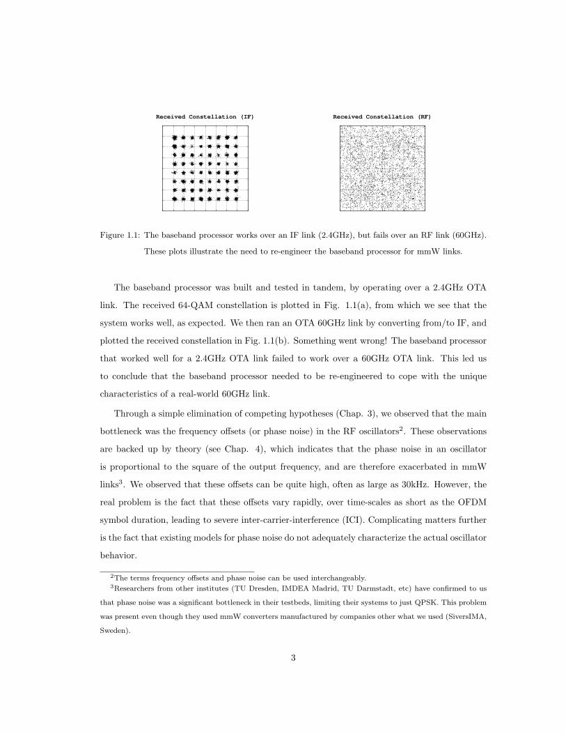
Received Constellation (IF) Received Constellation (RF)
Figure 1.1: The baseband processor works over an IF link (2.4GHz), but fails over an RF link (60GHz).
These plots illustrate the need to re-engineer the baseband processor for mmW links.
The baseband processor was built and tested in tandem, by operating over a 2.4GHz OTA
link. The received 64-QAM constellation is plotted in Fig. 1.1(a), from which we see that the
system works well, as expected. We then ran an OTA 60GHz link by converting from/to IF, and
plotted the received constellation in Fig. 1.1(b). Something went wrong! The baseband processor
that worked well for a 2.4GHz OTA link failed to work over a 60GHz OTA link. This led us
to conclude that the baseband processor needed to be re-engineered to cope with the unique
characteristics of a real-world 60GHz link.
Through a simple elimination of competing hypotheses (Chap. 3), we observed that the main
bottleneck was the frequency offsets (or phase noise) in the RF oscillators2. These observations
are backed up by theory (see Chap. 4), which indicates that the phase noise in an oscillator
is proportional to the square of the output frequency, and are therefore exacerbated in mmW
links3. We observed that these offsets can be quite high, often as large as 30kHz. However, the
real problem is the fact that these offsets vary rapidly, over time-scales as short as the OFDM
symbol duration, leading to severe inter-carrier-interference (ICI). Complicating matters further
is the fact that existing models for phase noise do not adequately characterize the actual oscillator
behavior.
2The terms frequency offsets and phase noise can be used interchangeably.3Researchers from other institutes (TU Dresden, IMDEA Madrid, TU Darmstadt, etc) have confirmed to us
that phase noise was a significant bottleneck in their testbeds, limiting their systems to just QPSK. This problem
was present even though they used mmW converters manufactured by companies other what we used (SiversIMA,
Sweden).
3

In this thesis, we discuss existing phase noise models, and show that experimental observations
do not match the behavior predicted by these models (Chap. 4). We then present a measurement-
driven model for phase noise, which accurately characterizes the oscillator behavior (Chap. 5).
We then present Iris, a time-domain technique to compensate for the large amounts of phase
noise (Chap. 6). Iris measures these offsets on a per-symbol basis and performs the correction in
the time-domain on a buffered version of the same symbol. By performing the de-rotation in the
time-domain, Iris is able to mitigate the effects of ICI, thereby providing significant improvements
in the SER. Further, by measuring the offsets and performing the correction on the same symbol,
Iris is able to prevent performance degradation even in cases where the frequency offsets exhibit
high variations over very short time-scales. We show that over real hardware, Iris provides one
to two orders of magnitude reductions in the SER as compared to the existing state of the art,
over real-world mmW links at 60GHz.
As mentioned earlier, this thesis emphasizes the engineering of a real-world 60GHz OTA link
as a means to design and test various baseband processing techniques. In the next chapter,
we describe the testbed, along with the software architecture for this implementation. Without
further ado, let us get on with it.
4
Chapter 2
Testbed and Implementation
We first describe the hardware and software components needed to run the testbed. We then
describe the architecture of the baseband processor that we built from scratch.
2.1 Testbed
Our testbed is built on the PXI platform from NI. The development was started on LabView
2013, but was later migrated to LabView 2014 SP1. The transmitter and receiver operate on
two separate boxes, each of which have the parts listed below.
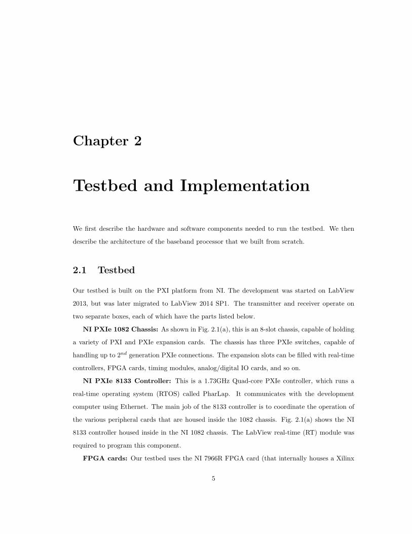
NI PXIe 1082 Chassis: As shown in Fig. 2.1(a), this is an 8-slot chassis, capable of holding
a variety of PXI and PXIe expansion cards. The chassis has three PXIe switches, capable of
handling up to 2nd generation PXIe connections. The expansion slots can be filled with real-time
controllers, FPGA cards, timing modules, analog/digital IO cards, and so on.
NI PXIe 8133 Controller: This is a 1.73GHz Quad-core PXIe controller, which runs a
real-time operating system (RTOS) called PharLap. It communicates with the development
computer using Ethernet. The main job of the 8133 controller is to coordinate the operation of
the various peripheral cards that are housed inside the 1082 chassis. Fig. 2.1(a) shows the NI
8133 controller housed inside in the NI 1082 chassis. The LabView real-time (RT) module was
required to program this component.
FPGA cards: Our testbed uses the NI 7966R FPGA card (that internally houses a Xilinx
5

Figure 2.1: a) The NI 1082 PXIe chassis with the NI PXIe 8133 controller housed inside. b) The Sivers
FC1005V mmW converter. Note: Both images are courtesy of their respective manufacturers.
Vitrex-5 FPGA), as well as the NI 7976R FPGA card (that internally houses a Xilinx Kintek-7
FPGA). The FPGAs do all the baseband signal processing, and communicate with each other
through the PXIe backplane if they need to. The LabView FPGA module was required to
program the FPGA cards. In order to compile the FPGA bitfiles, the Xilinx compilation modules
for LabView (14.7 ISE and 2013.4 Vivado) were required.
NI 5791 FAM: This FlexRIO adapter module (FAM) card is a converter between the
baseband signal (that feeds to/from the FPGA card) and the IF signal (that is connected to
the antenna). Its transceiver supports up to 130MHz bandwidth (100MHz at 3dB loss), and
frequencies of up to 4.4GHz. Depending on the frequency, it can support up to 20dBm of
input/output IF power. In our testbed, the signal from the 5791 FAM can be sent out over a
whip antenna, directional patch antenna, or through an SMA cable to the receiver.
Sivers FC1005V mmW Converters: At the transmitter, the IF signal from the NI 5791
FAM can be up-converted to mmW in the range of 57−63GHz using the FC1005V board. On this
board, the IF signal is mixed with the output of a local oscillator (LO), filtered, amplified, and
sent over a WR-15 waveguide output. We use horn antennas (manufactured by Sage millimeter)
to interface with the WR-15 waveguide. This converter works in tandem with power supply and
controller card, also made by Sivers. An identical converter at the receiver performs the down-
conversion from mmW RF to IF. The converter is shown in Fig. 2.1(b). This board internally
uses a Hittite HMC736LP4 GaAs InGaP heterojunction bipolar transistor to implement a voltage
controlled oscillator (up to 15GHz). Frequency multipliers are used to create the LO in the desired
6
Transmitter RT(NI 8133)
Transmitter FPGA(NI 7966R)
Front-endFAM
(NI 5791)
mmWConverter
(Sivers)
Figure 2.2: Overall architecture of the transmitter. The output of the NI 5791 is the IF signal, which
can be directly transmitted, or further up-converted to mmW using the Sivers module.
frequency range.
Miscellaneous: Our testbed also uses several other components such as the HP ESA L1500A
spectrum analyzer, a Tektronix AFG 3022C function generator, various horn and patch antennas,
and SMA cables manufactured by MegaPhase.
2.2 Software Architecture
2.2.1 Transmitter
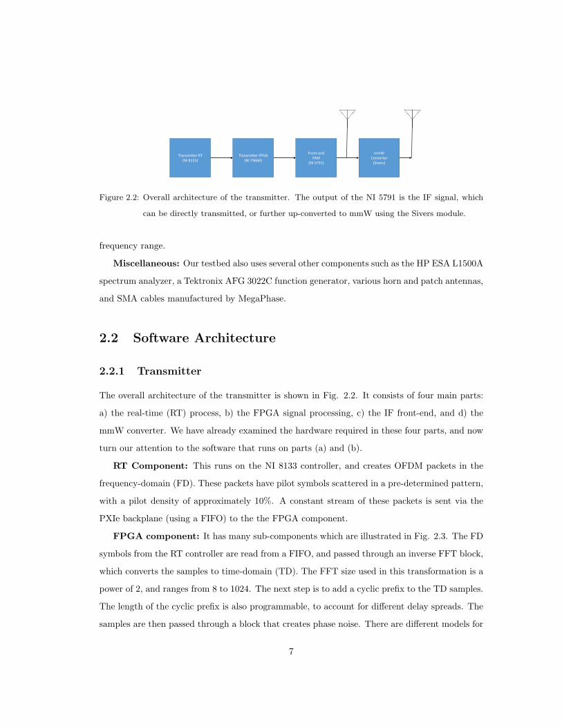
The overall architecture of the transmitter is shown in Fig. 2.2. It consists of four main parts:
a) the real-time (RT) process, b) the FPGA signal processing, c) the IF front-end, and d) the
mmW converter. We have already examined the hardware required in these four parts, and now
turn our attention to the software that runs on parts (a) and (b).
RT Component: This runs on the NI 8133 controller, and creates OFDM packets in the
frequency-domain (FD). These packets have pilot symbols scattered in a pre-determined pattern,
with a pilot density of approximately 10%. A constant stream of these packets is sent via the
PXIe backplane (using a FIFO) to the the FPGA component.
FPGA component: It has many sub-components which are illustrated in Fig. 2.3. The FD
symbols from the RT controller are read from a FIFO, and passed through an inverse FFT block,
which converts the samples to time-domain (TD). The FFT size used in this transformation is a
power of 2, and ranges from 8 to 1024. The next step is to add a cyclic prefix to the TD samples.
The length of the cyclic prefix is also programmable, to account for different delay spreads. The
samples are then passed through a block that creates phase noise. There are different models for
7

Read FD symbols from RT
IFFT(FD to TD)
Cyclicprefixer
Phase noise emulation
Multipath emulation
Correct IQ impairments
To NI 5791 FAM
Figure 2.3: Architecture of the FPGA component of the transmitter. The components have been engi-
neered for maximum flexibility and run-time reconfiguration. These components all fit on a
single NI 7966R FPGA board.
phase noise creation, and we visit these models in Chap. 4 and 5. The samples are then passed
through a time-varying FIR filter, which simulates the multi-path profile of the channel. The
circuitry can be configured to bypass this block completely, for OTA experiments. The samples
are then passed through a block that corrects for the IQ impairments that were measured in
the FAM at the time of manufacture. These IQ impairments include in-line gain and cross-gain.
Finally, the samples are appropriately scaled and sent to the NI 5791 FAM.
2.2.2 Receiver
Similar to the overall structure of the transmitter, the overall architecture of the receiver (Fig.
2.4) consists of four main parts: a) the RT process, c) the FPGA signal processor, c) the IF
front-end, and d) the mmW converter. The input to the NI 5791 FAM is an IF signal that can
come from one of two sources: a) directly from an antenna, if the transmission is over IF, or b)
the received mmW signal down-converted to IF by the Sivers module.
The main difference however, is in the FPGA component. From Fig. 2.4, we can see that the
FPGA functionality has been split between a primary and secondary FPGA. The reason is this
project started out as an examination of various equalization techniques; the design was therefore
split across two FPGAs, where the bulk of the signal processing was done on the primary, and just
the equalization was done on the secondary. This main benefit of this design was the speeding
up the FPGA compilation cycles. Fig. 2.5 illustrates the design of the primary FPGA, showing
8

ReceiverRT
(NI 8133)
PrimaryFPGA
(NI 7966R)
Front-endFAM
(NI 5791)
mmWConverter
(Sivers)
PhysicalSelector
SecondaryFPGA
(NI 7976R orNI 7966R)
Figure 2.4: Overall architecture of the receiver. The input of the NI 5791 is the IF signal, received
directly through an antenna, or as the result of down-converting a received mmW signal
(using the Sivers module).
From NI 5791 FAMCorrect IQ
impairmentsPacketize
TD phase noise correction (Iris)
Remove cyclic prefix
Reorder FFT output
To secondary FPGA for equalization
FFT(TD to FD)
FD phase noise correction
Timing offset estimation
Figure 2.5: Architecture of the FPGA component (Primary) of the receiver. The components have been
engineered for maximum flexibility and run-time reconfiguration. These components all fit
on a single NI 7966R FPGA board.
its sub-components.
Primary FPGA: The NI 5791 FAM sends a stream of time-domain complex baseband
samples to the primary FPGA. The first step is to correct the IQ impairments. The timing
offsets (or, packet boundaries) are estimated using Schmidl-Cox [5], which assumes that the first
symbol of the packet has two identical halves. Once the packet boundaries have been established,
the phase noise is corrected using Iris1. The cyclic prefix is removed, and the packet is converted
to FD using an FFT block. The residual phase noise is then corrected in the frequency domain,
1As we shall see, Iris is the main contribution in this thesis, helping to mitigate phase noise, and thereby reduce
the symbol error rate by one to two orders of magnitude.
9

Figure 2.6: Architecture of the secondary component of the receiver FPGA architecture. Its basic job is
to perform equalization, and to send the following to the receiver RT host: a) the equalized
constellation; and b) the symbol error rate. Depending on the equalizer used, the secondary
fits on either the NI 7966R or NI 7976R FPGA board.
by tracking the common phase error (CPE). The packet is then sent to the secondary FPGA.
Secondary FPGA: The main task of the secondary FPGA is to perform equalization. As
illustrated in Fig. 2.6, the secondary FPGA sends the post-equalized symbols to the RT host,
along with the measured symbol error rates. We had implemented many equalizers (linear, trian-
gulation, SINC interpolation, decision directed feedback equalization, and Vulcan2). However for
the rest of this thesis, we consider only Linear equalization, as it is the most widely implemented
in real systems, and is the most resource efficient.
Summary: The architecture described in this chapter allows great flexibility in the design and
testing of various baseband processing blocks. This flexibility also allowed us to run experiments
that were designed for specific measurements, other than raw symbol error rates. For example,
we could easily design and run experiments that allowed us to test various hypotheses for the
behavior observed in Fig. 1.1. In the next chapter, we examine these hypotheses, and describe
experiments to test them.
2 This work started out as the design and implementation of a new equalizer (Vulcan), which could handle
the exacerbated frequency offsets and Doppler shifts in mmW systems. However, we later realized that the sheer
amounts of phase noise meant that the equalizer was not the bottleneck. The Vulcan project then morphed into
the Iris project, which aimed to mitigate phase noise.
10

Chapter 3
Eliminating Hypotheses
In Fig. 1.1, we observed that while the IF link (2.4GHz carrier) worked well, the RF link (60GHz
carrier) completely failed. In this chapter, we investigate these observations, develop hypotheses
that explain this behavior, and describe experiments to test these hypotheses.
3.1 Basic Sinusoidal Test
The first test was to see whether a basic sinusoidal signal could be sent from the transmitter to
the receiver. We modified the transmitter RT component (see Fig. 2.2) to create the OFDM
packet in such a way that only one subcarrier (k) was used, with the others nulled out. The same
QPSK symbol was transmitted on the subcarrier k, on all symbol indices. This packet structure
Figure 3.1: Structure of the OFDM packet used for debugging. Only one subcarrier is used, and the
others are nulled out. The same QPSK symbol is transmitted on every symbol index on the
chosen subcarrier.
11
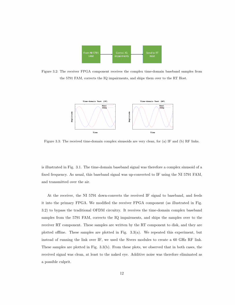
Figure 3.2: The receiver FPGA component receives the complex time-domain baseband samples from
the 5791 FAM, corrects the IQ impairments, and ships them over to the RT Host.
Amplitude
Time
Time-domain Test (IF)
RealImag
Amplitude
Time
Time-domain Test (RF)
RealImag
Figure 3.3: The received time-domain complex sinusoids are very clean, for (a) IF and (b) RF links.
is illustrated in Fig. 3.1. The time-domain baseband signal was therefore a complex sinusoid of a
fixed frequency. As usual, this baseband signal was up-converted to IF using the NI 5791 FAM,
and transmitted over the air.
At the receiver, the NI 5791 down-converts the received IF signal to baseband, and feeds
it into the primary FPGA. We modified the receiver FPGA component (as illustrated in Fig.
3.2) to bypass the traditional OFDM circuitry. It receives the time-domain complex baseband
samples from the 5791 FAM, corrects the IQ impairments, and ships the samples over to the
receiver RT component. These samples are written by the RT component to disk, and they are
plotted offline. These samples are plotted in Fig. 3.3(a). We repeated this experiment, but
instead of running the link over IF, we used the Sivers modules to create a 60 GHz RF link.
These samples are plotted in Fig. 3.3(b). From these plots, we observed that in both cases, the
received signal was clean, at least to the naked eye. Additive noise was therefore eliminated as
a possible culprit.
12

Figure 3.4: The receiver FPGA architecture was re-designed for the frequency-domain test to debug the
system. The output is a stream r[i] which captures the relationship between the symbol i
and the previous symbol (i− 1). This test enabled us to conclude that phase noise was the
main bottleneck in our RF system.
3.2 Frequency-domain (FD) Test
After eliminating additive noise as a culprit, we turned our attention to analyzing the signal in the
frequency domain. The transmitter was identical to that in the basic sinusoidal experiment, where
the transmitted OFDM packet had a known symbol on subcarrier k, with all other subcarriers
nulled out. The receiver FPGA component was re-designed (and plotted in Fig. 3.4) as described
below.
The time-domain samples from the 5791 FAM were first passed through a block to correct
the IQ impairments. The timing offsets were estimated, and the incoming stream was broken
up into packets, each with a fixed number of symbols. The cyclic prefixes were removed, and
the signal was converted to frequency-domain using an FFT block. The output corresponding to
subcarrier index k was passed on, and all other subcarriers were discarded. Call this stream S[i],
where i is the symbol index. We then implemented a block that simply calculated the following:
r[i] = S[i]S∗[i− 1] (3.1)
where * denotes complex conjugation. This stream r[i] was sent from the receiver FPGA com-
ponent to the RT component, where it was plotted.
Understanding the stream r[i]: The stream r[i] represents the relationship between sym-
13

-10
-5
0
5
10
-10 -5 0 5 10
Imaginary
Real
25 kHz Constant Offset
-10
-5
0
5
10
-10 -5 0 5 10
Imaginary
Real
Variable Gains
Figure 3.5: Understanding the behavior of r[i] through simulated conditions. (a) Under constant fre-
quency offsets, the phase of r[i] is proportional to the frequency offset. A rotation of 2π
corresponds to an offset equal to the subcarrier bandwidth. (b) Under variable gains, the
magnitude of r[i] varies, but the phase remains 0.
bol S[i] and the previous symbol S[i−1]. The magnitude of r[i] is the product of the magnitudes
of symbol S[i] and S[i − 1]. The phase of r[i] is the relative rotation (in frequency-domain)
between S[i] and S[i − 1]. It can be shown that this rotation is proportional to the frequency
offset between the transmitter and receiver oscillators. Before plotting the r[i] values from real
experiments, we use Fig. 3.5 to explain how r[i] behaves under different simulated1 conditions:
• Constant frequency offsets: A phase rotation of 2π radian corresponds to an offset equal to
the subcarrier bandwidth. Therefore, as plotted in Fig. 3.5(a), a constant offset of −25kHz
results in a phase of about −71 degrees or −1.23 radian, since the subcarrier bandwidth
in this experiment is 127kHz. Recall that the channel bandwidth is 130MHz, and the FFT
size (number of subcarriers) is 1024.
• Variable gains: If the amplifier exhibits variable gains, then the magnitude of r[i] will also
vary, as shown in Fig. 3.5(b). The phase of r[i] remains 0.
1 The simulated phenomena were: a) frequency offsets, and b) variable amplifier gains. In order to run these
experiments, the baseband time-domain signal from the transmitter was passed through a block (also implemented
on the FPGA) that could digitally create frequency offsets using a numerically controlled oscillator (NCO), as
well as perform a variable scaling on the samples to simulate time-varying amplifier gains. The transmitter and
receiver were then connected by a cable, which carried the IF signal.
14
-10
-5
0
5
10
-10 -5 0 5 10
Imaginary
Real
Frequency-domain Test (IF)
-10
-5
0
5
10
-10 -5 0 5 10
Imaginary
Real
Frequency-domain Test (RF)
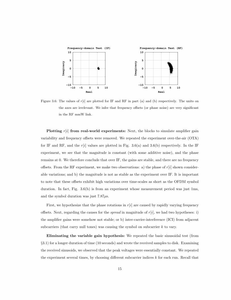
Figure 3.6: The values of r[i] are plotted for IF and RF in part (a) and (b) respectively. The units on
the axes are irrelevant. We infer that frequency offsets (or phase noise) are very significant
in the RF mmW link.
Plotting r[i] from real-world experiments: Next, the blocks to simulate amplifier gain
variability and frequency offsets were removed. We repeated the experiment over-the-air (OTA)
for IF and RF, and the r[i] values are plotted in Fig. 3.6(a) and 3.6(b) respectively. In the IF
experiment, we see that the magnitude is constant (with some additive noise), and the phase
remains at 0. We therefore conclude that over IF, the gains are stable, and there are no frequency
offsets. From the RF experiment, we make two observations: a) the phase of r[i] shown consider-
able variations; and b) the magnitude is not as stable as the experiment over IF. It is important
to note that these offsets exhibit high variations over time-scales as short as the OFDM symbol
duration. In fact, Fig. 3.6(b) is from an experiment whose measurement period was just 1ms,
and the symbol duration was just 7.87µs.
First, we hypothesize that the phase rotations in r[i] are caused by rapidly varying frequency
offsets. Next, regarding the causes for the spread in magnitude of r[i], we had two hypotheses: i)
the amplifier gains were somehow not stable; or b) inter-carrier-interference (ICI) from adjacent
subcarriers (that carry null tones) was causing the symbol on subcarrier k to vary.
Eliminating the variable gain hypothesis: We repeated the basic sinusoidal test (from
§3.1) for a longer duration of time (10 seconds) and wrote the received samples to disk. Examining
the received sinusoids, we observed that the peak voltages were essentially constant. We repeated
the experiment several times, by choosing different subcarrier indices k for each run. Recall that
15

the choice of subcarrier index k determines the frequency of the resulting sinusoidal signal in time-
domain. For all values of k, we observed that the peak voltages over the observation interval
were constant. We therefore eliminated variable amplifier gains as the cause of the magnitude
variations.
Confirming the phase-noise hypothesis: The results of the frequency-domain experiment
led us to hypothesize that phase noise was causing the r[i] values to exhibit the following: a)
phase rotations, and b) a slight spreading in the magnitude. We now describe two experiments
to test these hypotheses.
In the first experiment, we used a shorter symbol duration. The FFT size was 512, which led
to a symbol duration of 3.94µs, and the subcarrier bandwidth being approximately 254kHz. We
observed a similar behavior as shown in Fig. 3.6(b), but with the angular spread significantly
reduced, as plotted in Fig. 3.7(a). This is because the subcarrier bandwidth has increased by
a factor of 2, as compared with the previous experiment which used an FFT size of 1024. This
observation was consistent with our hypothesis of phase noise.
In the second experiment, we reverted to FFT size 1024, and used two adjacent subcarriers k
and k + 1. The transmitter used the QPSK symbol (1 + i) on subcarrier k and symbol (−1− i)
on subcarrier k + 1. The receiver was unchanged; it plotted the r[i] values for subcarrier k
and discarded the rest. These values are plotted in Fig. 3.7(b), from which we observe that
the magnitude of r[i] exhibited great variations. These observations are consistent with inter-
carrier-interference (ICI); the QPSK symbol (−1− i) on subcarrier k+ 1 destructively interferes
with QPSK symbol (1 + i) on subcarrier k in varying amounts, depending on the instantaneous
frequency offset.
These two experiments bolstered our hypothesis that rapidly-varying frequency offsets (or
phase noise) was causing severe inter-carrier-interference (ICI). This ICI can explain Fig. 1.1,
where we observed that the 64-QAM constellation was clean over an IF link, but was completely
destroyed over RF. In the next chapter, we study phase noise in greater detail by investigating the
following issues: a) the source of phase noise; b) oscillator quality; c) existing phase noise models
(which fail to accurately characterize our observations); and d) a proposed Gaussian phase noise
model.
16

-10
-5
0
5
10
-10 -5 0 5 10
Imaginary
Real
FD Test (RF, FFT size 512)
-10
-5
0
5
10
-10 -5 0 5 10
Imaginary
Real
FD Test (RF, 2 Subcarriers)
Figure 3.7: Confirming the phase-noise hypothesis through additional experiments on r[i]. In a) we use
a shorter symbol duration, and therefore a greater subcarrier width, by setting the FFT size
to 512. The angular spread of r[i] is therefore reduced, as compared to the case where the
FFT size was 1024. In b) we transmit QPSK symbols on adjacent subcarriers, such that
they destructively interfere with each other, in the presence of frequency offsets. These plots
confirm our hypothesis that phase noise is the bottleneck in our mmW testbed.
17
Chapter 4
Phase Noise in mmW Systems
Oscillators are important components in wireless systems, which along with synthesizers and
clock recovery units, are responsible for synchronizing the transmitter and receiver devices. In
practical radios, the frequency of the oscillator are controllable over some range, using voltage
controlled oscillators (VCOs). In the simplest sense, an oscillator is a non-linear active circuit
that converts DC power to an AC sinusoidal waveform1. The output of an ideal sinusoidal
oscillator is given by:
s(t) = cos(2πfct+ θ) (4.1)
where fc is the carrier frequency in Hertz, and θ is an arbitrary and fixed phase reference. The
spectrum of this ideal oscillator is a simple peak at fc and is 0 everywhere else, as illustrated in
Fig. 4.2(a). A useful framework to study a real oscillator is a linear feedback model, as illustrated
in Fig. 4.1. The first component of this model is an amplifier whose gain A is a function of the
frequency f . The second component is a bandpass filter with transfer function β(f). It can
be shown that the relationship between the output voltage Vo and the input voltage Vi can be
expressed as:
Vo
Vi=
A(f)1− β(f)A(f)
(4.2)
1See [6] for a detailed discussion on RF oscillators. We have attempted to distill and present the most relevant
information in this chapter.
18
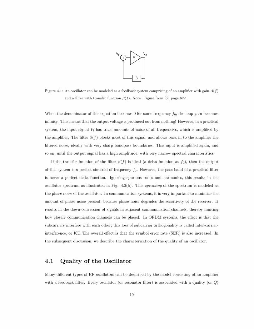
Figure 4.1: An oscillator can be modeled as a feedback system comprising of an amplifier with gain A(f)
and a filter with transfer function β(f). Note: Figure from [6], page 622.
When the denominator of this equation becomes 0 for some frequency f0, the loop gain becomes
infinity. This means that the output voltage is produced out from nothing! However, in a practical
system, the input signal Vi has trace amounts of noise of all frequencies, which is amplified by
the amplifier. The filter β(f) blocks most of this signal, and allows back in to the amplifier the
filtered noise, ideally with very sharp bandpass boundaries. This input is amplified again, and
so on, until the output signal has a high amplitude, with very narrow spectral characteristics.
If the transfer function of the filter β(f) is ideal (a delta function at f0), then the output
of this system is a perfect sinusoid of frequency f0. However, the pass-band of a practical filter
is never a perfect delta function. Ignoring spurious tones and harmonics, this results in the
oscillator spectrum as illustrated in Fig. 4.2(b). This spreading of the spectrum is modeled as
the phase noise of the oscillator. In communication systems, it is very important to minimize the
amount of phase noise present, because phase noise degrades the sensitivity of the receiver. It
results in the down-conversion of signals in adjacent communication channels, thereby limiting
how closely communication channels can be placed. In OFDM systems, the effect is that the
subcarriers interfere with each other; this loss of subcarrier orthogonality is called inter-carrier-
interference, or ICI. The overall effect is that the symbol error rate (SER) is also increased. In
the subsequent discussion, we describe the characterization of the quality of an oscillator.
4.1 Quality of the Oscillator
Many different types of RF oscillators can be described by the model consisting of an amplifier
with a feedback filter. Every oscillator (or resonator filter) is associated with a quality (or Q)
19
𝑓𝑐 𝑓𝑐
Figure 4.2: (a) Spectrum of an ideal oscillator of frequency fc Hertz. (b) The spectrum of a real oscillator
has most of its power concentrated around fc, but phase noise causes the power to spread
out as shown.
factor. Higher the Q factor, closer is the behavior of the filter to ideal. There are several
advantages of high-Q oscillators: a) stable operational frequency, over process and time; b)
narrower band-pass characteristics; and c) higher order harmonics are removed, leading to a
clean output sinusoid.
Unfortunately, high-Q oscillators are very hard to fabricate onto integrated circuits (ICs).
Examples of such oscillators include quartz crystals, dielectric pucks, ferro-electric devices, mag-
netic devices, and magneto-static wave films. Low-Q oscillators can be fabricated onto an IC,
and examples include RLC (resistance, inductance, capacitance) resonator tanks and distributed
transmission lines with varactor loading.
RLC Resonators: This are the most common type of resonator used in ICs made from
silicon or other semiconductors. The reasons for their ubiquity are their low power consumption,
tunability, and ease of fabrication. Their small signal equivalent circuit is represented either as
a parallel or as a series RLC circuit. Note that L is the inductance, C is the capacitance, and
R is the loss resistance of the circuit. These two representations are equivalent, and are plotted
in Fig. 4.3. In the figure, Rs and Rp indicate the resistance in the series and parallel versions
respectively. The conversions between the series and parallel equivalent circuits, along with the
mathematical relations that tie the R, L, and C values to the Q of the the oscillator can be found
in [6].
RLC equivalent of high-Q Quartz oscillators: As explained in detail in [6], quartz
crystals are based on the piezo-electric effect, which converts electrical charge into mechanical
20

Figure 4.3: Conversion from the series to parallel equivalent RLC models. Note: Figure from [6], page
628.
Figure 4.4: Equivalent RLC model (small signal circuit model) of a quartz crystal oscillator. Note:
Figure from [6], page 628.
strain, and vice-versa. These oscillators have the highest Q, but are typically manufactured to
have an output frequency of between 2 and 60 MHz. Quartz crystal oscillators have an equivalent
RLC model, as shown in Fig. 4.4. It consists of a highly selective series resonant circuit formed
by Lm and Cm, which describe the mechanical oscillation mode in the crystal. Rs describes the
equivalent series resistance, and Cp is the parasitic capacitance associated with the contacts and
lead wires.
RLC resonator tanks fabricated on ICs are the most common type of RF oscillators in use.
However as mentioned earlier, they have low-Q, and suffer from significant phase noise. As we
shall see, this phase noise is exacerbated at high frequencies. In the next section, we examine
existing models for phase noise.
4.2 Current Models for Phase Noise
One way of visualizing the phase noise of an oscillator is by looking at the spectrum of the
oscillator output, as previously shown in Fig. 4.2(b). Greater amounts of phase noise lead to
21

𝑓m𝑓𝑜
𝑃ℎ𝑎𝑠𝑒 𝑁𝑜𝑖𝑠𝑒 in dBc/Hz
1𝐻𝑧 bandwidth
𝑃𝑠
𝑃𝑛
𝑃ℎ𝑎𝑠𝑒 𝑁𝑜𝑖𝑠𝑒 𝐹𝑙𝑜𝑜𝑟
Figure 4.5: The phase noise of an oscillator expressed as the power spectral density (PSD) of the θ(t)
process. It is expressed in dBc/Hz, and settles to a noise floor at large offset frequencies fm.
greater spread of the spectrum from the center frequency. This method is intuitive and renders the
phase noise easy to visualize. However, it turns out that describing the phase noise analytically
is rather difficult to do. This is because the noise is a very small signal perturbation of a large
signal at the terminals of the amplifier. Small signal approximations [7] are therefore insufficient
in this case. Large signal approximations are very complex, and their parameters are difficult to
measure. As a consequence, these models do not lead to an easy method to simulate the phase
noise. Therefore, the most useful formulation for phase noise is to model the output of a practical
oscillator as:
s(t) = cos(2πfct+ θ(t)) (4.3)
where θ(t) is the time-dependent phase noise in the oscillator output. The preferred method to
study phase noise is to model θ(t) as a Gaussian wide-sense stationary (WSS) process. Charac-
terizing the power spectral density (PSD) of this process provides a useful method to measure the
phase noise. The PSD of θ(t) is expressed in terms of its single-sideband (SSB) power density.
It is defined as the ratio of the noise power Pn in a 1Hz bandwidth at an offset fm to the power
at the fundamental frequency Ps. This phase noise is expressed in dBc/Hz, and is shown in the
equation below. It is also illustrated in Fig. 4.5.
L(Fm) = 10 log[Pn(fm, 1Hz)
Ps
](4.4)
Different models for phase noise have different expressions that the describe the PSD of the
22

θ(t) process. While there have been many such proposed models [8, 9, 10, 11, 12], we consider
two main models in this thesis: a) the classical Leeson’s model [11], and b) the state-of-the-art
IEEE model for 60GHz oscillators [12].
4.2.1 Leeson’s Model
Recall that an oscillator is essentially a non-linear device that converts DC power to an AC
sinusoidal signal. However, as with many non-linear circuits, it is useful to consider a simplified
linear model. The classical Leeson’s model considers the oscillator as a linear time invariant
(LTI) process. It describes the power spectral density (PSD) of the random process θ(t) by:
L(fm) = 10 log10
[2FkTPsig
(1 +
( f02Qfm
)2)(
1 +fcor
fm
)]dBc/Hz (4.5)
where F is a curve-fitting parameter, k is the Boltzmann constant, T is the temperature in Kelvin,
fm is the offset frequency at which the power is to be estimated, Psig is the oscillator output
power, Q is the quality factor of the oscillator, fcor is the corner frequency of the device, and f0 is
the output frequency of the oscillator. From this formulation, we make three main observations.
First, the phase noise increases as the square of the oscillator frequency; this is why phase noise
is exacerbated in mmW links. Further, when frequency multipliers are used, the phase noise is
exacerbated [13, 14]. Second, the Q-factor should ideally be as low as possible, which is a tall
task for oscillators fabricated on a chip. Finally, the phase noise is directly proportional to the
temperature of the device.
While a deeper examination of the intuition behind Leeson’s model is out of the scope of this
thesis, we point the reader to [15, 16, 17], which examine Leeson’s model from first principles.
Leeson’s model is generally treated as an exercise in curve-fitting. Ignoring the physical meaning
of the various constants, we can simplify Leeson’s model as follows:
L(fm) ∝ (c1 + fm2)(c2 + fm)fm
3 (4.6)
where c1 and c2 are constants. The phase noise is most significant at small offset frequencies fm,
where L(fm) varies as 1fm
3 . The main weakness of Leeson’s model is that it predicts unbounded
noise. As a result, it is not possible to even simulate a θ(t) stream using Leeson’s model. Due to
23

Filter withtransfer function
H0(z)
Filter withtransfer function
H1(z)
𝑤𝑘 𝞱𝑘 𝑑𝑘
Figure 4.6: White noise wk is filtered to get the θk process, which in turn is filtered to get the dk process.
The statistics of the dk process can be compared to that measured experimentally to validate
a phase noise model.
these weaknesses, we turn our attention toward the IEEE model for the phase noise of oscillators
in the 60GHz band.
4.2.2 IEEE Model
This model predicts the PSD of the θ(t) process as shown:
L(fm) = L(0)1 + (fm/fz)2
1 + (fm/fp)2(4.7)
where fm is the offset frequency, fz is the zero frequency, and fp is the pole frequency. There
are two important ways that the IEEE model is better than Leeson’s model. First, the IEEE
model predicts bounded noise, agreeing with empirical measurements. Second, simulating the
θ(t) process (or its discrete-time version θk) simply involves passing white Gaussian noise through
a filter with transfer function H0(z), as shown on the left side of Fig. 4.6. It can be shown that
this transfer function takes the general form:
H0(z) =1− αzz
−1
1− αpz−1(4.8)
where αz and αp are constants. This transfer function can be implemented by a simple first order
filter. Now, we turn our attention toward validating this phase noise model.
4.2.3 (In)Validating the IEEE Model
The goal of the experiment is to measure the amount of phase noise in the oscillator, and to
check if it is consistent with that predicted by the IEEE model. It is impossible to directly
measure θ(t) (or its discrete-time version θk) since our hardware does not give us access to the
24
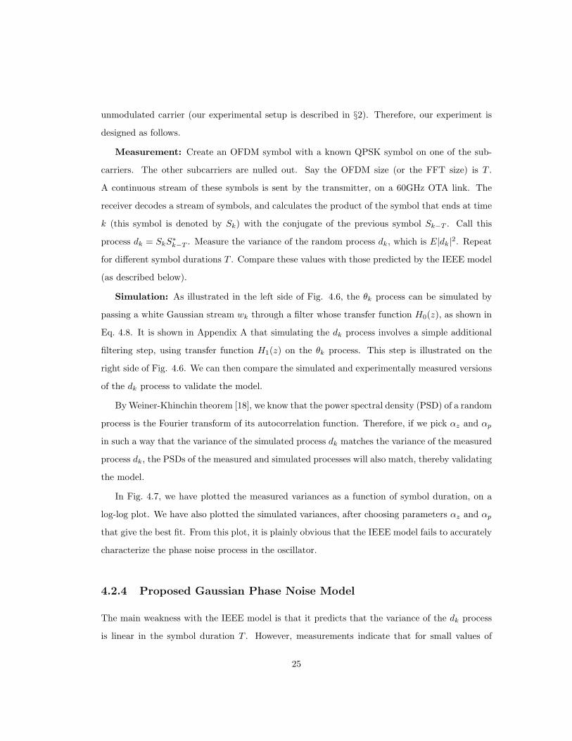
unmodulated carrier (our experimental setup is described in §2). Therefore, our experiment is
designed as follows.
Measurement: Create an OFDM symbol with a known QPSK symbol on one of the sub-
carriers. The other subcarriers are nulled out. Say the OFDM size (or the FFT size) is T .
A continuous stream of these symbols is sent by the transmitter, on a 60GHz OTA link. The
receiver decodes a stream of symbols, and calculates the product of the symbol that ends at time
k (this symbol is denoted by Sk) with the conjugate of the previous symbol Sk−T . Call this
process dk = SkS∗k−T . Measure the variance of the random process dk, which is E|dk|2. Repeat
for different symbol durations T . Compare these values with those predicted by the IEEE model
(as described below).
Simulation: As illustrated in the left side of Fig. 4.6, the θk process can be simulated by
passing a white Gaussian stream wk through a filter whose transfer function H0(z), as shown in
Eq. 4.8. It is shown in Appendix A that simulating the dk process involves a simple additional
filtering step, using transfer function H1(z) on the θk process. This step is illustrated on the
right side of Fig. 4.6. We can then compare the simulated and experimentally measured versions
of the dk process to validate the model.
By Weiner-Khinchin theorem [18], we know that the power spectral density (PSD) of a random
process is the Fourier transform of its autocorrelation function. Therefore, if we pick αz and αp
in such a way that the variance of the simulated process dk matches the variance of the measured
process dk, the PSDs of the measured and simulated processes will also match, thereby validating
the model.
In Fig. 4.7, we have plotted the measured variances as a function of symbol duration, on a
log-log plot. We have also plotted the simulated variances, after choosing parameters αz and αp
that give the best fit. From this plot, it is plainly obvious that the IEEE model fails to accurately
characterize the phase noise process in the oscillator.
4.2.4 Proposed Gaussian Phase Noise Model
The main weakness with the IEEE model is that it predicts that the variance of the dk process
is linear in the symbol duration T . However, measurements indicate that for small values of
25

10-2
10-1
100
101
102
103
100 101 102 103 104
Variance (Deg2)
Symbol Size (Samples)
MeasuredIEEE
Figure 4.7: Variance of the dk process as a function of the symbol or FFT size (T ). Observe that the
IEEE model predicts linear growth, whereas OTA measurements indicate that the variance
grows as O(T 2) for small T , and linear growth for larger T .
T , the variance of dk grows as O(T 2), and becomes linear for larger values of T . In order to
asymptotically match the experimental variances, we propose a new Gaussian phase noise model
for θk. Recall that in the IEEE model, the θk process was obtained by passing wk through a
filter with the transfer function H0(z) shown in Eq. 4.8. Our proposed Gaussian model contains
an additional integrator, and its transfer function is shown below:
H0(z) =(1− αzz
−1)(1− αpz−1)(1− z−1)
(4.9)
As we did with the IEEE model, we simulate the variances of the dk process under our proposed
Gaussian model, and compare the variances with those that were experimentally measured. In
Fig. 4.8, we have plotted the measured variances as a function of the symbol duration, on a
log-log plot. We have also plotted the variances from simulating our proposed Gaussian phase
noise model, shown in Eq. 4.9. From this figure, we can see that our proposed Gaussian phase
noise model agrees with the measured variances.
In order to further validate the model, we ran the following two-part experiment. In the first
part, we ran a 60GHz OTA link, and measured the SER for different FFT sizes, across different
SNRs. In the second part, we connected the transmitter and receiver over IF, and bypassed the
RF circuitry altogether. We created phase noise using the model shown in Eq. 4.9. Running the
experiments for different FFT sizes and different SNRs, we found that the SERs from the two
26

10-2
10-1
100
101
102
103
100 101 102 103 104
Variance (Deg2)
Symbol Size (Samples)
MeasuredProposed Gaussian
Figure 4.8: Variance of the dk process as a function of the symbol or FFT size (T ). Observe that our
proposed Gaussian phase noise model agrees with the measured variances.
parts of the experiment did not match.
The reason the proposed model failed is that it matched only the measured second-order
statistics (and first order) of the dk process, but did not match the higher order statistics. This
led us to conclude that the phase noise should not be modeled as a Gaussian WSS process, as
traditionally described in the literature. Instead, θk should be modeled as a non-Gaussian WSS
process, as done in the next section.
27

Chapter 5
Proposed Non-Gaussian Ramp
Model
In the previous chapter, we have seen that existing models for phase noise have several weaknesses.
Leeson’s model predicts unbounded noise, and is therefore not possible to simulate. The IEEE
model does not match the measured variances of the dk process. The Gaussian model that we
proposed in the previous chapter matches the second order statistics, but fails to match the SER
because of differing higher order statistics. This led us to fundamentally rethink how phase noise
should be modeled.
In this chapter, we present a model that is based on the observed behavior of the RF oscillator.
It does not have a closed-form mathematical structure, but is very simple to understand. The
random process in this model is the frequency offset at time k, denoted by γk. Before we describe
the model, we shall describe an experiment that logically leads to the model.
The experiment is similar to the one described in §4.2.3, where we experimentally measured
the dk values for different FFT sizes. Define βk as the angle of dk. If the FFT size is T , the
subcarrier bandwidth is BT , where B is the channel bandwidth measured in Hertz. The average
frequency offset over the duration of these two symbols is a random process γk, and is therefore
given by:
γk =βkB
2πTHz (5.1)
28
-15
-10
-5
0
5
10
15
0 20 40 60 80 100Freq Offset (kHz)
Symbol Index
Figure 5.1: Variations in the frequency offset (γk) over time. The FFT size is 1024 and the number of
symbols is 100. Observe the ramp like behavior, with additive noise.
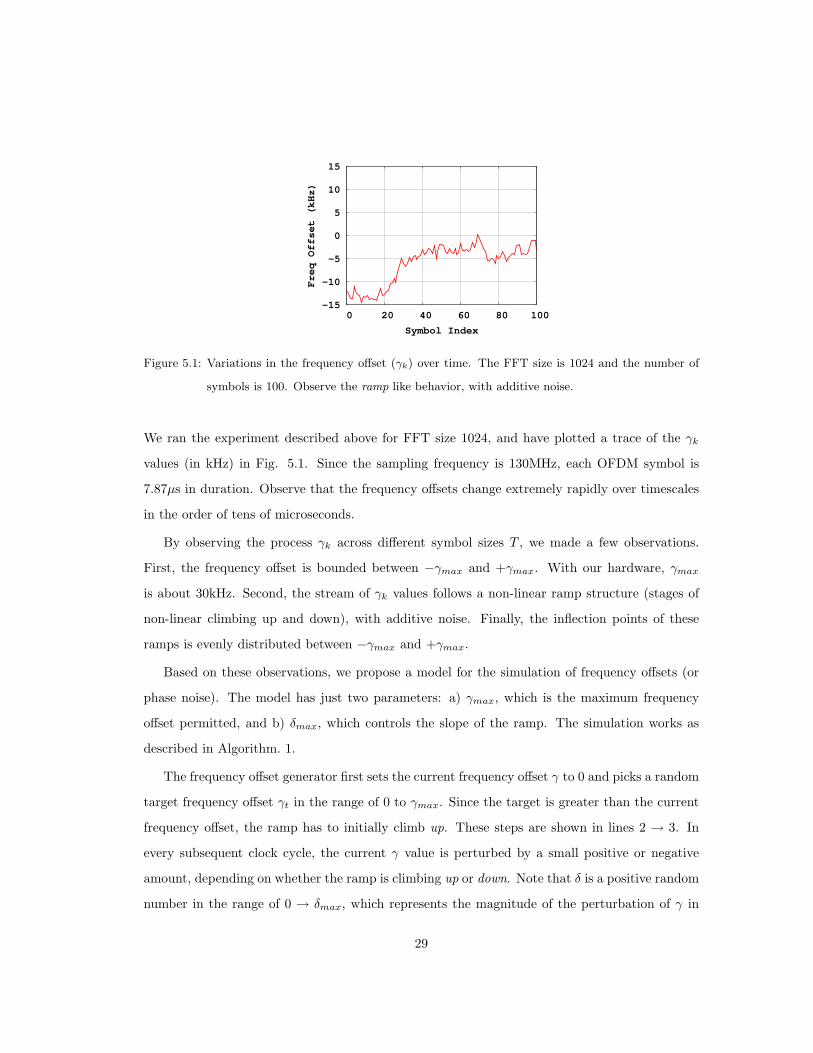
We ran the experiment described above for FFT size 1024, and have plotted a trace of the γk
values (in kHz) in Fig. 5.1. Since the sampling frequency is 130MHz, each OFDM symbol is
7.87µs in duration. Observe that the frequency offsets change extremely rapidly over timescales
in the order of tens of microseconds.
By observing the process γk across different symbol sizes T , we made a few observations.
First, the frequency offset is bounded between −γmax and +γmax. With our hardware, γmax
is about 30kHz. Second, the stream of γk values follows a non-linear ramp structure (stages of
non-linear climbing up and down), with additive noise. Finally, the inflection points of these
ramps is evenly distributed between −γmax and +γmax.
Based on these observations, we propose a model for the simulation of frequency offsets (or
phase noise). The model has just two parameters: a) γmax, which is the maximum frequency
offset permitted, and b) δmax, which controls the slope of the ramp. The simulation works as
described in Algorithm. 1.
The frequency offset generator first sets the current frequency offset γ to 0 and picks a random
target frequency offset γt in the range of 0 to γmax. Since the target is greater than the current
frequency offset, the ramp has to initially climb up. These steps are shown in lines 2 → 3. In
every subsequent clock cycle, the current γ value is perturbed by a small positive or negative
amount, depending on whether the ramp is climbing up or down. Note that δ is a positive random
number in the range of 0 → δmax, which represents the magnitude of the perturbation of γ in
29

10-2
10-1
100
101
102
103
100 101 102 103 104Variance (Deg2)
Symbol Size (Samples)
MeasuredProposed Ramp
Figure 5.2: Variation in the dk process as a function of the symbol or FFT size (T ). Our proposed ramp
model produces variations in dk that match those from an over-the-air experiment at 60GHz.
the current clock cycle. Once the current offset γ reached the target γt, a new target is chosen
in the range of −γmax to +γmax, and the process repeats in the next clock cycle.
We make a few observations about the parameters γmax and δmax in the model. First, γmax
controls the maximum drift of the oscillator from ideal. This is determined experimentally by
observing the maximum drift of the oscillator, as shown in Eq. 5.1. Next, δmax controls the rate
of drift of the oscillator as a function of time. Care must be taken while setting this parameter,
as it depends on the clock rate of the discrete time simulator implementing this model. In our
setup, the clock rate is 130MHz. If the clock rate were to be increased by a factor of 2, we would
change δmax to half its value to provide the same emulated phase noise profile.
5.1 Validating the Model
We had previously attempted to validate the IEEE model (see §4.2.3) and a proposed Gaussian
phase noise model (see §4.2.4), by examining the variances of the dk process. The first step toward
validating our proposed ramp model is to compare the variances of the dk process observed in
two ways: a) over-the-air at 60GHz, and b) using the ramp to generate phase noise over a link
running over IF. This comparison is plotted in Fig. 5.2. Observe that the variances match very
closely. As we had seen in §4.2.4, this is a necessary (but not sufficient) condition to validate the
model.
30

The final step in validating this ramp model is to compare the symbol error rates. This
experiment was conducted in two parts. First, we measured the SER through an OTA experiment
at 60GHz for different symbol durations (FFT sizes), as well as across different SNRs. In the
second part, we ran the experiment over IF, but with phase noise generated using our ramp
model, and measured the SNRs. The SERs obtained from the two experiments were very close,
thereby validating the ramp model.
Given that we now understand the behavior of phase noise in the system, we turn our attention
to re-designing the baseband processor to mitigate its deleterious effects. In the next chapter we
present Iris, a time-domain technique that reduces the symbol error rate by one to two orders of
magnitude, by mitigating the effects of phase noise.
31

Algorithm 1 Simulate frequency offset.1: Input: γmax, δmax
2: γ ← 0 . Current frequency offset = 0
3: γt ← N(0→ +γmax) . Pick a target frequency offset that is ≥ 0
4: Climb ← ‘Up’ . Since the target offset is greater than the current offset
5: loop . This loop is executed once every clock cycle
6: δ ← N(0→ δmax) . Change in offset for this clock cycle
7: if Climb = ‘Up’ then
8: γ ← γ + δ . Climb up, so Increment current offset
9: if γ ≥ γt then
10: Reset ← True . Target reached.
11: end if
12: else
13: γ ← γ − δ . Climb down, so Decrement current offset
14: if γ ≥ γt then
15: Reset ← True . Target reached.
16: end if
17: end if
18: if Reset = True then
19: γt ← N(−γmax → +γmax) . Find a new target.
20: if γt ≥ γ then
21: Climb ← ‘Up’
22: else
23: Climb ← ‘Down’
24: end if
25: Reset ← ‘False’
26: end if
27: end loop
32
Chapter 6
Iris: Mitigating Phase Noise
In this chapter we propose Iris, a baseband technique that corrects the enormous amounts of
phase noise that we observed in mmW bands. Iris is computationally very simple, is suitable for
operation over wide bandwidths, and provides reductions in symbol error rates by one to two
orders of magnitude, as compared to existing state of the art. Before describing Iris, we briefly
describe existing techniques to mitigate phase noise.
6.1 Existing Techniques
Equalization: This is a frequency-domain technique that relies on known pilot symbols to be
scattered in the packet. By estimating the channel at these pilot locations, the receiver can
estimate the channel at non-pilot locations (through interpolation) and proceed to decode the
packet. However, as we observed in Chapter. 1, equalization simply could not cope with the
sheer amounts of phase noise in these mmW bands.
Tracking the Common Phase Error (CPE): This frequency-domain technique [19] transmits
a known QPSK pilot symbol on a fixed subcarrier on every OFDM symbol, as shown in Fig. 3.1.
It estimates the rotation that symbol i has undergone relative to the previous symbol (i − 1),
by making the measurement on the reference subcarrier. Once this rotation is measured, all the
subcarriers on the symbol are de-rotated by the same amount. As we shall see, this technique
works well only with small amounts of phase noise. As the phase noise is increased, the OFDM
33

Figure 6.1: Feedback loop to correct phase noise: The offsets are measured, and may be averaged. A
compensation signal is generated by the VCO, and this signal is used applied to correct the
frequency offsets in subsequent input samples.
subcarriers lose their orthogonality, and would have irreversibly interfered with each other by the
time this technique can be applied.
Schmidl-Cox: This technique [5] measures the frequency offset on a per-packet basis using
two reference OFDM symbols, and applies the correction to the remainder of the packet in the
time domain. By applying the correction in the time domain, ICI is eliminated. However, this
technique works well only if the frequency offsets are stable, even of they are large. Unfortunately,
as was illustrated in Fig. 5.1, the frequency offsets change very significantly even on a per-symbol
basis over mmW links, rendering this technique incapable of correcting ICI.
Feedback Loop: As illustrated in Fig. 6.1, This technique has two main components: a)
frequency offset measurement, and b) frequency offset correction. The offsets can be measured
either in the time domain (using the cyclic prefix), or in the frequency domain (using reference
pilot symbols). In a closed loop system, this offset (which may be optionally averaged) is fed back
to a numerically controlled oscillator (NCO), which applies the correction in the time domain. If
the offsets are stable, this technique provides good gains, very similar to Schmidl-Cox. Since the
feedback loop can be engineered to be quicker than the packet duration (unlike Schmidl-Cox),
this technique can provide some gains over Schmidl-Cox.
Tweaking OFDM Parameters: Since the oscillators exhibit such high variations, it stands
to reason that OFDM symbols of shorter durations (smaller FFT sizes) will be more resilient to
phase noise. Unfortunately, the solution of just using a smaller FFT size is not practical. Outdoor
wireless links over mmW can have delay spreads as large as 750ns, as indicated in [20, 21, 22]. The
cyclic prefix therefore has to be at least this length, in order to mitigate inter-symbol-interference
34

Figure 6.2: Iris uses a buffer to hold a copy of the time-domain samples of a symbol. Once the offsets
have been measured, the correction signal generated by the VCO is applied on the buffered
version of the same symbol, and the result is sent to the rest of the processing chain.
(ISI). Shorter symbol lengths imply that the time wasted on the cyclic prefix gets amortized over
a smaller amount of useful data, thereby leading to greater overheads. For example, the sampling
rate in our system is 130MS/s. Assuming that the cyclic prefix is 40 samples long (about 300ns),
FFT sizes of 128, 256, 512, and 1024 have their cyclic prefix overheads as approximately 31.25%,
15.6%, 7.8%, and 3.9% respectively. This is the reason why larger FFT sizes (such as 1024) are
preferred.
6.2 Description of Iris
Iris is a time-domain technique that corrects the phase noise on a per-symbol basis. Its schematic
has been illustrated in Fig. 6.2. First, the average frequency offset across a symbol is measured
using the cyclic prefix1. The time-domain samples of this symbol are held in a buffer for N + T
clock cycles. N is the number of clock cycles taken to calculate the frequency offset, after all the
samples of the current symbol have been received. In our implementation, N is just 45 samples.
T is the number of samples in the symbol, including the cyclic prefix. Once the average frequency
offset of a symbol is estimated, the buffered version of the symbol is de-rotated using an NCO,
and is then sent to the rest of the processing chain.
Resource Utilization: Iris is extremely resource-efficient, on account of its simplicity. It
requires buffer space for just one symbol (the number of samples is equal to the FFT size added
to the cyclic prefix size). It also needs a buffer for N samples, where N is the number of clock
1The offsets could also be measured in the frequency-domain, but the buffering requirements become larger.
35

cycles required to calculate the frequency offset in the symbol under measurement. It needs two
complex multipliers, one rectangular to polar converter, an accumulator, and an NCO (identical
to other feedback loop techniques).
6.3 Evaluation
In this section, we evaluate the performance of an OTA link at 60GHz in terms of the underlying
SER achieved. Across various SNRs, we evaluate the performance of the following six phase noise
mitigation techniques: (a) tracking the common phase error (CPE); (b) Iris; (c) Iris combined
with CPE; (d) Feedback Loop: This is time-domain Iris, where the measured frequency offset on
one symbol is corrected on the next symbol, instead of on the same symbol. This represents the
best-case behavior of a feedback loop, because of the short feedback time; (e) no phase correction
technique is applied at all, and f) the transmitter and receiver are connected by a cable, bypassing
the RF circuitry altogether, and operating directly over IF. All experiments are repeated for the
following FFT sizes: 128, 256, 512, and 1024. Further, all experiments are repeated for a range
of SNRs, in increments of 2dB. Finally, we repeat the experiments for 16-QAM and 64-QAM.
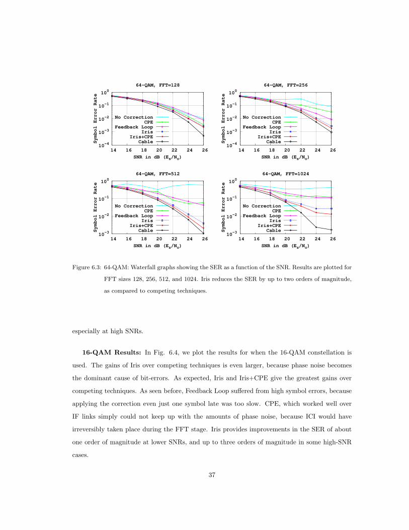
64-QAM Results: In Fig. 6.3, we plot the SER on the Y-axis, with the SNR (as Es
N0) on
the X-axis. The sub-plots represent different FFT sizes. For small symbol sizes (for example,
when the FFT size is 128), all techniques perform reasonably well. Iris is able to provide modest
gains (reduce the SER by up to a factor of 2) as compared to competing techniques, especially
at high SNRs. This is because at higher SNRs, the self-noise (caused by phase noise) becomes
dominant, and Iris is able to provide gains.
As the symbols get larger, the gains of Iris get even larger. Iris performs almost as well as
Iris+CPE, and Iris performs significantly better than CPE alone. This proves that the time-
domain corrections provide the bulk of the gains by mitigating ICI. Further, the Feedback Loop
technique also suffers from high SERs, even though it is a time-domain correction technique,
applied just one symbol late. This observation demonstrates the importance of applying the
corrections on the same symbol. We therefore conclude that techniques like Schmidl-Cox will
perform at most as well as the Feedback Loop. As compared to competing techniques, Iris
improves performance by up to an order of magnitude (sometimes, two orders of magnitude),
36
10-4
10-3
10-2
10-1
100
14 16 18 20 22 24 26
Symbol Error Rate
SNR in dB (Es/No)
64-QAM, FFT=128
No CorrectionCPE
Feedback LoopIris
Iris+CPECable
10-4
10-3
10-2
10-1
100
14 16 18 20 22 24 26
Symbol Error Rate
SNR in dB (Es/No)
64-QAM, FFT=256
No CorrectionCPE
Feedback LoopIris
Iris+CPECable
10-3
10-2
10-1
100
14 16 18 20 22 24 26
Symbol Error Rate
SNR in dB (Es/No)
64-QAM, FFT=512
No CorrectionCPE
Feedback LoopIris
Iris+CPECable
10-3
10-2
10-1
100
14 16 18 20 22 24 26
Symbol Error Rate
SNR in dB (Es/No)
64-QAM, FFT=1024
No CorrectionCPE
Feedback LoopIris
Iris+CPECable
Figure 6.3: 64-QAM: Waterfall graphs showing the SER as a function of the SNR. Results are plotted for
FFT sizes 128, 256, 512, and 1024. Iris reduces the SER by up to two orders of magnitude,
as compared to competing techniques.
especially at high SNRs.
16-QAM Results: In Fig. 6.4, we plot the results for when the 16-QAM constellation is
used. The gains of Iris over competing techniques is even larger, because phase noise becomes
the dominant cause of bit-errors. As expected, Iris and Iris+CPE give the greatest gains over
competing techniques. As seen before, Feedback Loop suffered from high symbol errors, because
applying the correction even just one symbol late was too slow. CPE, which worked well over
IF links simply could not keep up with the amounts of phase noise, because ICI would have
irreversibly taken place during the FFT stage. Iris provides improvements in the SER of about
one order of magnitude at lower SNRs, and up to three orders of magnitude in some high-SNR
cases.
37

10-710-610-510-410-310-210-1100
12 14 16 18 20 22 24
Symbol Error Rate
SNR in dB (Es/No)
16-QAM, FFT=128
No CorrectionCPE
Feedback LoopIris
Iris+CPECable
10-710-610-510-410-310-210-1100
12 14 16 18 20 22 24
Symbol Error Rate
SNR in dB (Es/No)
16-QAM, FFT=256
No CorrectionCPE
Feedback LoopIris
Iris+CPECable
10-710-610-510-410-310-210-1100
12 14 16 18 20 22 24
Symbol Error Rate
SNR in dB (Es/No)
16-QAM, FFT=512
No CorrectionCPE
Feedback LoopIris
Iris+CPECable
10-710-610-510-410-310-210-1100
12 14 16 18 20 22 24
Symbol Error Rate
SNR in dB (Es/No)
16-QAM, FFT=1024
No CorrectionCPE
Feedback LoopIris
Iris+CPECable
Figure 6.4: 16-QAM: Waterfall graphs showing the SER as a function of the SNR. Results are plotted for
FFT sizes 128, 256, 512, and 1024. Iris reduces the SER by up to two orders of magnitude,
as compared to competing techniques.
6.4 Constellation Plots
In the previous section, we have seen that Iris is able to reduce the symbol error rates by one
to two orders of magnitude, as compared to competing techniques. In this section, we plot
the resulting 64-QAM constellations obtained from different phase-noise mitigation techniques.
Recall from Fig. 1.1(b) that when the link was run over 60GHz, the constellation was completely
destroyed. In Fig. 6.5, we plot the received constellations under the following techniques: a)
estimation of the common phase error (CPE); b) feedback loops; c) Iris; and d) Iris combined
with CPE.
We observe that CPE provides some improvements, as compared to not using any correction
at all. However, the received constellation is still dirty, because ICI has already taken place by
38

CPE Feedback Loop
Iris Iris + CPE
Figure 6.5: Received 64-QAM constellations when different techniques are applied to mitigate phase
noise: a) tracking the error in the common phase error (CPE); b) feedback loop, with a loop
delay of just one symbol duration; c) Iris; and d) Iris combined with CPE. Iris combined with
CPE results in the best constellations, with a bulk of the performance improvement coming
from Iris.
the time this technique can be applied. The feedback loop technique is essentially Iris, but the
correction is applied just one symbol late. This represents the best-case behavior for feedback
loops, for two reasons: a) the correction is applied when the samples are perfectly aligned with the
symbol boundary; and b) the loop delay is just one symbol in duration. However, we observe that
despite the best-case implementation of feedback loops, the constellation is noisy. As mentioned
earlier, the reason for this behavior is that by the time the correction is applied, the current
frequency offsets would have changed.
When Iris is applied, we observe a visually obvious and noticeable improvement in the received
constellation. As seen earlier, this translates to a significant reduction in the symbol error rate.
Finally, when CPE is combined with Iris, the symbol error rates are further reduced, but is hard
to visualize on the received constellation plots.
39

Summary: Iris is extremely simple and computationally efficient. The amount of additional
resources that it requires are minimal, especially considering the fact that the SERs are improved
by one to two orders of magnitude. By measuring the phase noise on a symbol, and performing
the corrections on a buffered version of the same symbol, Iris is able to handle large amounts
of phase noise observed in these mmW bands. Performing the correction just one symbol late
leads to a dramatic increase in the SER, thereby demonstrating the importance of the buffering
stage. Finally, the benefit of Iris is easy to visualize through plots of the received constellation
symbols.
40

Chapter 7
Conclusion
Frequency offsets and phase noise have long been considered a solved problem in wireless systems.
In fact, to the best of our knowledge, there are only three techniques that existing radios use (see
§6.1) to solve this problem: a) feedback loops, b) tracking the common phase error (CPE), and c)
equalization. However, we experimentally observed that these techniques, even when combined
with each other, could not cope with the sheer amounts of phase noise present in mmW systems.
Complicating matters further was the fact that the experimentally observed phase noise patterns
could not be explained by existing models.
In this thesis, we made main two contributions toward modeling phase noise: a) invalidation
of the IEEE model for 60GHz oscillators, and b) we proposed a new ramp model that fit the
experimental observations about the θ(t) process as well as the resulting symbol error rates.
However, the most important contribution in this thesis is the design and testing of Iris, a time-
domain technique that measures the offsets on a per-symbol basis, and corrects the same symbol
in the time-domain. Iris is simple, resource-efficient, and is suitable for operation over high
bandwidth links. Through our experiments we show that Iris enables higher-order modulations
(such as 64-QAM), even in the presence of previously fatal amounts of phase noise.
41

Appendix A
Derivation for phase noise filters
In Chap. 4, we had seen that the θk process could be simulated by passing white Gaussian noise
wk through a filter with transfer function H0(z). In this appendix, we extend the discussion to
show that the inter-symbol rotation process dk can just as easily be simulated by passing the θk
process through a filter with transfer function H1(z).
For the received symbol ending at time k, the average rotation that the symbol undergoes
is given by φk and is also a random process. The relationship between the θk and φk random
processes is shown below (first in time domain, followed by frequency domain):
φk =1T
T−1∑l=0
θk−l (A.1)
Φ(z) =1T
T−1∑l=0
z−lΘ(z) (A.2)
In the frequency domain, the filter that gets us from the random process θk to the random process
φk is shown:
G1(z) =Φ(z)Θ(z)
=1− z−T
T (1− z−1)(A.3)
Next, the symbol-to-symbol rotation is denoted by the random process dk as shown below (first
in time domain, followed by frequency domain):
dk = φk − φk−T (A.4)
D(z) = Φ(z)− z−T Φ(z) (A.5)
42

In the frequency domain, the filter that gets us from the random process φk to the random
process dk is shown:
G2(z) =D(z)Φ(z)
= 1− z−T (A.6)
Therefore, the relationship between the D(z) process and the Θ(z) process is shown below:
D(z) = G2(z)G1(z)Θ(z) (A.7)
The filters G1(z) and G2(z) can be combined into H1(z) as shown:
D(z) = H1(z)Θ(z) (A.8)
We have shown that simulating the dk process involves passing the θk process through a filter
with transfer function H1(z). Once we know the transfer function H1(z), calculating the actual
filter taps is trivial.
43

Bibliography
[1] R. Daniels, J. Murdock, T. S. Rappaport, and R. Heath. 60 GHz Wireless: Up Close and
Personal. IEEE Microwave Magazine, 11(7):44 – 50, December 2010.
[2] T. S. Rappaport, E. Ben-Dor, J.N. Murdock, and Y. Qiao. 38 GHz and 60 GHz angle-
dependent propagation for cellular and peer-to-peer wireless communications. Proc. IEEE
ICC, pages 4568–4573, June 2012.
[3] NI PXI Platform. http://www.ni.com/pxi/.
[4] SiversIMA FC1005V/00 converter. http://siversima.com/product/fc1005v00/.
[5] Timothy M Schmidl and Donald C Cox. Robust frequency and timing synchronization for
ofdm. Communications, IEEE Transactions on, 45(12):1613–1621, 1997.
[6] Sorin Voinigescu. High-frequency integrated circuits. Cambridge University Press, 2013.
[7] Andrea Mazzanti, Francesco Svelto, and Pietro Andreani. On the amplitude and phase errors
of quadrature lc-tank cmos oscillators. Solid-State Circuits, IEEE Journal of, 41(6):1305–
1313, 2006.
[8] Thomas H Lee and Ali Hajimiri. Oscillator phase noise: a tutorial. Solid-State Circuits,
IEEE Journal of, 35(3):326–336, 2000.
[9] JJ Rael and Asad A Abidi. Physical processes of phase noise in differential lc oscillators. In
Custom Integrated Circuits Conference, 2000. CICC. Proceedings of the IEEE 2000, pages
569–572. IEEE, 2000.
44
[10] Behzad Razavi. A study of phase noise in cmos oscillators. Solid-State Circuits, IEEE
Journal of, 31(3):331–343, 1996.
[11] David B Leeson. A simple model of feedback oscillator noise spectrum. Proceedings of the
IEEE, pages 329–330, 1966.
[12] Chang-Soon Choi, et al. RF impairment models for 60GHz-band SYS/PHY simulation. doc:
IEEE 802.15-06-0477-01-003c. November 2006.
[13] Fred L Walls and Andrea Demarchi. Rf spectrum of a signal after frequency multiplication;
measurement and comparison with a simple calculation. Instrumentation and Measurement,
IEEE Transactions on, 24(3):210–217, 1975.
[14] KW Tang, S Leung, N Tieu, P Schvan, and SP Voinigescu. Frequency scaling and topology
comparison of millimeter-wave cmos vcos. In Compound Semiconductor Integrated Circuit
Symposium, 2006. CSIC 2006. IEEE, pages 55–58. IEEE, 2006.
[15] Ali Hajimiri and Thomas H Lee. A general theory of phase noise in electrical oscillators.
Solid-State Circuits, IEEE Journal of, 33(2):179–194, 1998.
[16] Xianhe Huang, Feng Tan, Wei Wei, and Wei Fu. A revisit to phase noise model of leeson.
In Frequency Control Symposium, 2007 Joint with the 21st European Frequency and Time
Forum. IEEE International, pages 238–241. IEEE, 2007.
[17] Jean-Christophe Nallatamby, Michel Prigent, Marc Camiade, and Juan Obregon. Phase
noise in oscillators-leeson formula revisited. Microwave Theory and Techniques, IEEE Trans-
actions on, 51(4):1386–1394, 2003.
[18] John Proakis and Masoud Salehi. Digital communications, 2008.
[19] Paul H Moose. A technique for orthogonal frequency division multiplexing frequency offset
correction. Communications, IEEE Transactions on, 42(10):2908–2914, 1994.
[20] Theodore S Rappaport, Shu Sun, Rimma Mayzus, Hang Zhao, Yaniv Azar, Kangping Wang,
George N Wong, Jocelyn K Schulz, Mathew Samimi, and Felix Gutierrez. Millimeter wave
mobile communications for 5g cellular: It will work! Access, IEEE, 1:335–349, 2013.
45

[21] Theodore S Rappaport, Felix Gutierrez, Eyal Ben-Dor, James N Murdock, Yijun Qiao,
Jonathan Tamir, et al. Broadband millimeter-wave propagation measurements and models
using adaptive-beam antennas for outdoor urban cellular communications. Antennas and
Propagation, IEEE Transactions on, 61(4):1850–1859, 2013.
[22] Theodore S Rappaport, James N Murdock, and Felix Gutierrez. State of the art in 60-
ghz integrated circuits and systems for wireless communications. Proceedings of the IEEE,
99(8):1390–1436, 2011.
46