irgb/ib/s/p4620d-epbf product datasheet
TRANSCRIPT

IR IGBT IRGB4620DPbF IRGIB4620DPbF
IRGP4620D(-E)PbF IRGS4620DPbF
Base part number Package Type Standard Pack Orderable Part Number Form Quantity
IRGB4620DPbF TO-220AB Tube 50 IRGB4620DPbF
IRGP4620DPbF TO-247AC Tube 25 IRGP4620DPbF IRGP4620D-EPbF TO-247AD Tube 25 IRGP4620D-EPbF
Tube 50 IRGS4620DPbF IRGS4620DPbF D2Pak Tape and Reel Right 800 IRGS4620DTRRPbF
Tape and Reel Left 800 IRGS4620DTRLPbF
IRGIB4620DPbF TO-220AB Full-Pak Tube 50 IRGIB4620DPbF
VCES = 600V
IC = 20A, TC =100°C
tSC ≥ 5µs, TJ(max) = 175°C
VCE(ON) typ. = 1.55V @ IC = 12A
Applications
• Industrial Motor Drive
• Inverters
• UPS
• Welding
Features Benefits
Low VCE(ON) and switching losses High efficiency in a wide range of applications and switching frequencies
Square RBSOA and maximum junction temperature 175°C Improved reliability due to rugged hard switching performance and high power capability
Positive VCE (ON) temperature coefficient Excellent current sharing in parallel operation 5µs Short Circuit SOA Enables short circuit protection scheme Lead-Free, RoHS Compliant Environmentally friendly
Insulated Gate Bipolar Transistor with Ultrafast Soft Recovery Diode
G C E Gate Collector Emitter
IRGP4620DPbF TO-247AC
E
G
n-channel
C
IRGS4620DPbF D2Pak
IRGIB4620DPbF TO-220AB Full-Pak
C E
G
C C
C E
G
IRGP4620D-EPbF TO-247AD
C E
G
C
IRGB4620DPbF TO-220AB
C E
C
G
E C G
1 2015-11-23

IRGB/IB/P/SP4620D/EPbF
2 2015-11-23
Absolute Maximum Ratings
Parameter Max. Units
VCES Collector-to-Emitter Voltage 600 V IC @ TC = 25°C Continuous Collector Current 32
A IC @ TC = 100°C Continuous Collector Current 20 ICM Pulse Collector Current, VGE = 15V 36 ILM Clamped Inductive Load Current, VGE = 20V 48 IF @ TC = 25°C Diode Continuous Forward Current 16 IF @ TC = 100°C Diode Continuous Forward Current 10
VGE Continuous Gate-to-Emitter Voltage ±20 V
PD @ TC = 25°C Maximum Power Dissipation 140 W
PD @ TC = 100°C Maximum Power Dissipation 70 TJ Operating Junction and -40 to +175
C TSTG Storage Temperature Range Soldering Temperature, for 10 sec. (1.6mm from case) 300 Mounting Torque, 6-32 or M3 Screw (TO-220, TO-247) 10 lbf·in (1.1 N·m)
IFM Diode Maximum Forward Current 48
Transient Gate to Emitter Voltage ±30
Thermal Resistance Parameter Min. Typ. Max. Units Thermal Resistance Junction-to-Case (D2Pak, TO-220) ––– ––– 1.07
°C/W RθCS Thermal Resistance, Case-to-Sink (flat, greased surface-TO-220, D2Pak, TO-220 Full-Pak ) ––– 0.50 –––
RθJA Thermal Resistance, Junction-to-Ambient (PCB Mount - D2Pak) ––– ––– 40
Thermal Resistance Junction-to-Case (D2Pak, TO-220) ––– ––– 3.66 Thermal Resistance Junction-to-Case (TO-247) ––– ––– 1.12
Thermal Resistance Junction-to-Case (TO-247) ––– ––– 3.71
Thermal Resistance, Junction-to-Ambient (Socket Mount –TO-247) ––– ––– 40 Thermal Resistance, Junction-to-Ambient (Socket Mount –TO-220) ––– ––– 62
RθJC (IGBT) Thermal Resistance Junction-to-Case (TO-220 Full-Pak) ––– ––– 3.75
RθJC (Diode) Thermal Resistance Junction-to-Case (TO-220 Full-Pak) ––– ––– 6.22
Thermal Resistance Case-to-Sink (TO-247) ––– 0.24 –––
Thermal Resistance, Junction-to-Ambient (Socket Mount –TO-220 Full-Pak) ––– ––– 65
Electrical Characteristics @ TJ = 25°C (unless otherwise specified) Parameter Min. Typ. Max. Units Conditions V(BR)CES Collector-to-Emitter Breakdown Voltage 600 — — V VGE = 0V, IC = 100µA ΔV(BR)CES/ΔTJ Temperature Coeff. of Breakdown Voltage — 0.40 — V/°C VGE = 0V, IC = 1mA (25°C-175°C)
VCE(on) Collector-to-Emitter Saturation Voltage — 1.55 1.85 IC = 12A, VGE = 15V, TJ = 25°C — 1.90 — IC = 12A, VGE = 15V, TJ = 150°C
VGE(th) Gate Threshold Voltage 4.0 — 6.5 V VCE = VGE, IC = 350µA ΔVGE(th)/ΔTJ Threshold Voltage Temp. Coefficient — -18 — mV/°C VCE = VGE, IC = 1.0mA (25°C-175°C) gfe Forward Transconductance — 7.7 — S VCE = 50V, IC = 12A, PW = 80µs
ICES Collector-to-Emitter Leakage Current — 2.0 — µA VGE = 0V, VCE = 600V — 475 — VGE = 0V, VCE = 600V, TJ = 175°C
IGES Gate-to-Emitter Leakage Current — — ±100 nA VGE = ±20V
VFM Diode Forward Voltage Drop — 2.1 3.1 V IF = 12A — 1.6 — IF = 12A, TJ = 175°C
— 1.97 — IC = 12A, VGE = 15V, TJ = 175°C V

IRGB/IB/P/SP4620D/EPbF
3 2015-11-23
Switching Characteristics @ TJ = 25°C (unless otherwise specified) Parameter Min. Typ. Max Units Conditions Qg Total Gate Charge — 25 —
nC IC = 12A
Qge Gate-to-Emitter Charge — 7.0 — VGE = 15V Qgc Gate-to-Collector Charge — 11 — VCC = 400V Eon Turn-On Switching Loss — 75 —
µJ IC = 12A, VCC = 400V, VGE=15V
RG = 22Ω, L = 200µH, LS = 150nH, TJ = 25°C
Energy losses include tail & diode reverse recovery
Eoff Turn-Off Switching Loss — 225 — Etotal Total Switching Loss — 300 — td(on) Turn-On delay time — 31 —
ns tr Rise time — 17 — td(off) Turn-Off delay time — 83 — tf Fall time — 24 — Eon Turn-On Switching Loss — 185 —
µJ IC = 12A, VCC = 400V, VGE=15V
RG = 22Ω, L = 200µH, LS = 150nH, TJ = 175°C
Energy losses include tail & diode reverse recovery
Eoff Turn-Off Switching Loss — 355 — Etotal Total Switching Loss — 540 — td(on) Turn-On delay time — 30 —
ns tr Rise time — 18 — td(off) Turn-Off delay time — 102 — tf Fall time — 41 — Cies Input Capacitance — 765 — VGE = 0V Coes Output Capacitance — 52 — pF VCC = 30V Cres Reverse Transfer Capacitance — 23 — f = 1.0MHz
RBSOA Reverse Bias Safe Operating Area TJ = 175°C, IC = 48A
FULL SQUARE VCC = 480V, Vp ≤ 600V RG = 22Ω, VGE = +20V to 0V
SCSOA Short Circuit Safe Operating Area 5.0 — — µs VCC = 400V, Vp ≤ 600V RG = 22Ω, VGE = +15V to 0V
Erec Reverse Recovery Energy of the Diode — 280 — µJ TJ = 175°C trr Diode Reverse Recovery Time — 68 — ns VCC = 400V, IF = 12A, VGE = 15V, Irr Peak Reverse Recovery Current — 19 — A Rg = 22Ω, L = 200µH, LS = 150nH
Notes: Limited by maximum junction temperature. Not applicable for Full-Pak package:current value limited by Rθ JC.
Rθ is measured at TJ of approximately 90°C. Refer to AN-1086 for guidelines for measuring V(BR)CES safely. Pulse width limited by maximum junction temperature. Values influenced by parasitic L and C in measurement. When mounted on 1” square PCB (FR-4 or G-10 Material). For recommended footprint and soldering techniques refer to application note #AN-994.http://www.irf.com/technical-info/appnotes/an-994.pdf VCC = 80% (VCES), VGE = 20V, L = 100µH, RG = 22Ω.
IRGB/IB/P/SP4620D/EPbF
4 2015-11-23
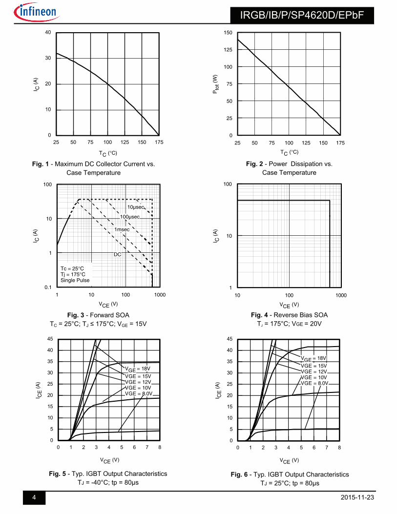
25 50 75 100 125 150 175
TC (°C)
0
10
20
30
40I C
(A
)
1 10 100 1000
VCE (V)
0.1
1
10
100
I C (A
) 1msec
10µsec
100µsec
Tc = 25°CTj = 175°CSingle Pulse
DC
Fig. 1 - Maximum DC Collector Current vs. Case Temperature
10 100 1000
VCE (V)
1
10
100
I C (A
)
Fig. 4 - Reverse Bias SOA TJ = 175°C; VGE = 20V
0 1 2 3 4 5 6 7 8
VCE (V)
0
5
10
15
20
25
30
35
40
45
I CE
(A)
VGE = 18VVGE = 15VVGE = 12VVGE = 10VVGE = 8.0V
Fig. 3 - Forward SOA TC = 25°C; TJ ≤ 175°C; VGE = 15V
Fig. 5 - Typ. IGBT Output Characteristics TJ = -40°C; tp = 80µs
0 1 2 3 4 5 6 7 8
VCE (V)
0
5
10
15
20
25
30
35
40
45
I CE
(A)
VGE = 18VVGE = 15VVGE = 12VVGE = 10VVGE = 8.0V
Fig. 6 - Typ. IGBT Output Characteristics TJ = 25°C; tp = 80µs
25 50 75 100 125 150 175
TC (°C)
0
25
50
75
100
125
150
Pto
t (W
)
Fig. 2 - Power Dissipation vs. Case Temperature

IRGB/IB/P/SP4620D/EPbF
5 2015-11-23
0.0 1.0 2.0 3.0 4.0
VF (V)
0
10
20
30
40
50
60
70
80
I F (
A)
-40°c25°C
175°C
5 10 15 20
VGE (V)
0
2
4
6
8
10
12
14
16
18
20
VC
E (
V) ICE = 6.0A
ICE = 12AICE = 24A
Fig. 8 - Typ. Diode Forward Voltage Drop Characteristics
0 1 2 3 4 5 6 7 8
VCE (V)
0
5
10
15
20
25
30
35
40
45I C
E (A
)VGE = 18VVGE = 15VVGE = 12VVGE = 10VVGE = 8.0V
5 10 15 20
VGE (V)
0
2
4
6
8
10
12
14
16
18
20
VC
E (
V) ICE = 6.0A
ICE = 12AICE = 24A
Fig. 7 - Typ. IGBT Output Characteristics TJ = 175°C; tp = 80µs
5 10 15 20
VGE (V)
0
2
4
6
8
10
12
14
16
18
20
VC
E (
V) ICE = 6.0A
ICE = 12AICE = 24A
Fig. 9 - Typical VCE vs. VGE TJ = -40°C
0 5 10 15
VGE (V)
0
10
20
30
40
50
I CE
(A
)
TJ = 25°CTJ = 175°C
Fig. 10 - Typical VCE vs. VGE TJ = 25°C
Fig. 12 - Typ. Transfer Characteristics VCE = 50V; tp = 10µs
Fig. 11 - Typical VCE vs. VGE
TJ = 175°C

IRGB/IB/P/SP4620D/EPbF
6 2015-11-23
5 10 15 20 25
IC (A)
1
10
100
1000
Sw
ichi
ng T
ime
(ns)
tR
tdOFF
tF
tdON
0 25 50 75 100 125
RG (Ω)
10
100
1000
Sw
ichi
ng T
ime
(ns)
tR
tdOFF
tF
tdON
Fig. 14 - Typ. Switching Time vs. IC
TJ = 175°C; L = 200µH; VCE = 400V, RG = 22Ω; VGE = 15V
0 10 20 30
IF (A)
0
5
10
15
20
25
I RR
(A)
RG = 10Ω
RG = 22Ω
RG = 47Ω
RG = 100Ω
Fig. 15 - Typ. Energy Loss vs. RG TJ = 175°C; L = 200µH; VCE = 400V, ICE = 12A; VGE = 15V
0 10 20 30
IC (A)
0
100
200
300
400
500
600
700
800E
nerg
y (µ
J)
EOFF
EON
0 25 50 75 100 125
Rg (Ω)
50
100
150
200
250
300
350
400
450
500
Ene
rgy
(µJ)
EOFF
EON
Fig. 13 - Typ. Energy Loss vs. IC
TJ = 175°C; L = 200µH; VCE = 400V, RG = 22Ω; VGE = 15V
0 25 50 75 100 125
RG (Ω)
5
10
15
20
25
I RR
(A)
Fig. 16 - Typ. Switching Time vs. RG TJ = 175°C; L = 200µH; VCE = 400V, ICE = 12A; VGE = 15V
Fig. 17 - Typ. Diode IRR vs. IF TJ = 175°C
Fig. 18 - Typ. Diode IRR vs. RG TJ = 175°C

IRGB/IB/P/SP4620D/EPbF
7 2015-11-23
0 500 1000 1500
diF /dt (A/µs)
200
400
600
800
1000
1200
1400
QR
R (
µC)
10Ω
22Ω
100Ω
47Ω
12A
24A
6.0A
8 10 12 14 16 18
VGE (V)
0
2
4
6
8
10
12
14
16
18
20
Tim
e (µ
s)
20
30
40
50
60
70
80
90
100
110
120
Cu
rrent (A
)
Fig. 20 - Typ. Diode QRR vs. diF/dt VCC = 400V; VGE = 15V; TJ = 175°C
0 10 20 30
IF (A)
0
50
100
150
200
250
300
350
400
Ene
rgy
(µJ)
RG = 10Ω
RG = 22Ω
RG = 47Ω
RG = 100Ω
0 20 40 60 80 100
VCE (V)
10
100
1000
10000
Cap
acita
nce
(pF
) Cies
Coes
Cres
Fig. 21 - Typ. Diode ERR vs. IF TJ = 175°C
0 500 1000 1500
diF /dt (A/µs)
0
5
10
15
20
25I R
R (A
)
Fig. 19 - Typ. Diode IRR vs. diF/dt VCC = 400V; VGE = 15V; IF = 12A; TJ = 175°C
0 5 10 15 20 25 30
Q G, Total Gate Charge (nC)
0
2
4
6
8
10
12
14
16
VG
E, G
ate-
to-E
mitt
er V
olta
ge (V
) VCES = 300V
VCES = 400V
Fig. 22 - VGE vs. Short Circuit Time VCC = 400V; TC = 25°C
Fig. 23 - Typ. Capacitance vs. VCE VGE= 0V; f = 1MHz
Fig. 24 - Typical Gate Charge vs. VGE ICE = 12A; L = 600µH

IRGB/IB/P/SP4620D/EPbF
8 2015-11-23
1E-006 1E-005 0.0001 0.001 0.01 0.1 1
t1 , Rectangular Pulse Duration (sec)
0.001
0.01
0.1
1
10
The
rmal
Res
pons
e ( Z
thJC
)
0.20
0.10
D = 0.50
0.02
0.01
0.05
SINGLE PULSE( THERMAL RESPONSE ) Notes:
1. Duty Factor D = t1/t22. Peak Tj = P dm x Zthjc + Tc
1E-006 1E-005 0.0001 0.001 0.01 0.1 1
t1 , Rectangular Pulse Duration (sec)
0.001
0.01
0.1
1
10
Ther
mal
Res
pons
e ( Z
thJC
)
0.20
0.10
D = 0.50
0.02
0.01
0.05
SINGLE PULSE( THERMAL RESPONSE ) Notes:
1. Duty Factor D = t1/t22. Peak Tj = P dm x Zthjc + Tc
Fig. 25 - Maximum Transient Thermal Impedance, Junction-to-Case (IGBT-TO-220Pak)
Fig. 26 - Maximum Transient Thermal Impedance, Junction-to-Case (DIODE-TO-220Pak)
τJ
τJ
τ1
τ1τ2
τ2 τ3
τ3
R1
R1R2
R2R3
R3
τC
τC
Ci= τi/RiCi= τi/Ri
Ri (°C/W) τi (sec)
0.358 0.000171
0.424 0.001361
0.287 0.009475
τJ
τJ
τ1
τ1τ2
τ2 τ3
τ3
R1
R1R2
R2R3
R3
τC
τC
Ci= τi/RiCi= τi/Ri
Ri (°C/W) τi (sec)
0.821094 0.000233
1.913817 0.001894
0.926641 0.014711

IRGB/IB/P/SP4620D/EPbF
9 2015-11-23
Fig.C.T.1 - Gate Charge Circuit (turn-off) Fig.C.T.2 - RBSOA Circuit
Fig.C.T.3 - S.C. SOA Circuit Fig.C.T.4 - Switching Loss Circuit
Fig.C.T.5 - Resistive Load Circuit Fig.C.T.6 - BVCES Filter Circuit
0
1K
VCCDUT
L
L
Rg
80 V
DUT VCC
+-
DC
4X
DUT
VCC
RSH
L
Rg
VCCDUT /DRIVER
diode clamp /DUT
-5V
Rg
VCCDUT
R = VCC
ICM
G force
C sense
100K
DUT0.0075µF
D1 22K
E force
C force
E sense

IRGB/IB/P/SP4620D/EPbF
10 2015-11-23
Fig. WF1 - Typ. Turn-off Loss Waveform @ TJ = 175°C using Fig. CT.4
Fig. WF2 - Typ. Turn-on Loss Waveform @ TJ = 175°C using Fig. CT.4
Fig. WF4 - Typ. S.C. Waveform
@ TJ = 150°C using Fig. CT.3
Fig. WF3 - Typ. Diode Recovery Waveform @ TJ = 175°C using Fig. CT.4
-25
-20
-15
-10
-5
0
5
10
15
20
25
-0.05 0.05 0.15
time (µS)
IRR
(A)
Peak
IRR
QRR
tRR
10%PeakIRR
-100
0
100
200
300
400
500
-5.00 0.00 5.00 10.00
time (µS)
VC
E (V
)
-50
0
50
100
150
200
250
ICE
(A)
VCE
ICE
-5
0
5
10
15
20
25
-100
0
100
200
300
400
500
-0.50 0.50 1.50
I CE
(A)
VC
E(V
)
Time(µs)
EOFF Loss
5% VCE
5% ICE
90% ICE
tf
-10
0
10
20
30
40
50
-100
0
100
200
300
400
500
11.70 11.90 12.10
I CE
(A)
VC
E(V
)
Time (µs)
EON
TEST
90% test
10% test current
5% VCE
tr

IRGB/IB/P/SP4620D/EPbF
11 2015-11-23
L O T C O D E 1 7 8 9
E X A M P L E : T H I S I S A N I R F 1 0 1 0
N o t e : "P " i n a s s e m b l y l i n e p o s i t i o ni n d i c a t e s "L e a d - F r e e "
I N T H E A S S E M B L Y L I N E "C "
A S S E M B L E D O N W W 1 9 , 2 0 0 0I N T E R N A T I O N A L P A R T N U M B E R
R E C T I F I E R
L O T C O D EA S S E M B L Y
L O G O
Y E A R 0 = 2 0 0 0
D A T E C O D E
W E E K 1 9
L I N E C
TO-220AB package is not recommended for Surface Mount Application.
TO-220AB Part Marking Information
TO-220AB Package Outline (Dimensions are shown in millimeters (inches))

IRGB/IB/P/SP4620D/EPbF
12 2015-11-23
TO-220AB Full-Pak package is not recommended for Surface Mount Application.
TO-220AB Full– Pak Part Marking Information
TO-220AB Full– Pak Package Outline (Dimensions are shown in millimeters (inches))

IRGB/IB/P/SP4620D/EPbF
13 2015-11-23
TO-247AC Package Outline Dimensions are shown in millimeters (inches)
TO-247AC Part Marking Information
TO-247AC package is not recommended for Surface Mount Application.
YEAR 1 = 2001
DATE CODE
PART NUMBERINTERNATIONAL
LOGORECTIFIER
ASSEMBLY
56 57
IRFPE30
135H
LINE Hindicates "Lead-Free" WEEK 35LOT CODE
IN THE ASSEMBLY LINE "H"
ASSEMBLED ON WW 35, 2001
Notes: This part marking information applies to devices produced after 02/26/2001
Note: "P" in assembly line position
EXAMPLE:WITH ASSEMBLY THIS IS AN IRFPE30
LOT CODE 5657

IRGB/IB/P/SP4620D/EPbF
14 2015-11-23
TO-247AD Package Outline Dimensions are shown in millimeters (inches)
TO-247AD Part Marking Information
TO-247AD package is not recommended for Surface Mount Application.
A S S E M B L Y Y E A R 0 = 2 0 0 0
A S S E M B L E D O N W W 3 5 , 2 0 0 0
IN T H E A S S E M B L Y L IN E "H "
E X A M P L E : T H IS IS A N IR G P 3 0 B 1 2 0 K D - E
L O T C O D E 5 6 5 7W IT H A S S E M B L Y P A R T N U M B E R
D A T E C O D E
IN T E R N A T IO N A LR E C T IF IE R
L O G O 0 3 5 H
5 6 5 7
W E E K 3 5
L IN E H
L O T C O D EN o te : "P " in a s s e m b ly l in e p o s it io n
in d ic a te s "L e a d - F re e "

IRGB/IB/P/SP4620D/EPbF
15 2015-11-23
D2-PAK (TO-263AB) Package Outline Dimensions are shown in millimeters (inches)
D2-Pak (TO-263AB) Part Marking Information
DATE CODE
YEAR 0 = 2000
WEEK 02
A = ASSEMBLY SITE CODE
RECTIFIERINTERNATIONAL
PART NUMBER
P = DESIGNATES LEAD - FREEPRODUCT (OPTIONAL)
F530SIN THE ASSEMBLY LINE "L"
ASSEMBLED ON WW 02, 2000
THIS IS AN IRF530S WITHLOT CODE 8024 INTERNATIONAL
LOGORECTIFIER
LOT CODEASSEMBLY
YEAR 0 = 2000
PART NUMBER
DATE CODE
LINE L
WEEK 02
OR
F530SLOGO
ASSEMBLYLOT CODE

IRGB/IB/P/SP4620D/EPbF
16 2015-11-23
3
4
4
TRR
FEED DIRECTION
1.85 (.073)1.65 (.065)
1.60 (.063)1.50 (.059)
4.10 (.161)3.90 (.153)
TRL
FEED DIRECTION
10.90 (.429)10.70 (.421)
16.10 (.634)15.90 (.626)
1.75 (.069)1.25 (.049)
11.60 (.457)11.40 (.449)
15.42 (.609)15.22 (.601)
4.72 (.136)4.52 (.178)
24.30 (.957)23.90 (.941)
0.368 (.0145)0.342 (.0135)
1.60 (.063)1.50 (.059)
13.50 (.532)12.80 (.504)
330.00(14.173) MAX.
27.40 (1.079)23.90 (.941)
60.00 (2.362) MIN.
30.40 (1.197) MAX.
26.40 (1.039)24.40 (.961)
NOTES :1. COMFORMS TO EIA-418.2. CONTROLLING DIMENSION: MILLIMETER.3. DIMENSION MEASURED @ HUB.4. INCLUDES FLANGE DISTORTION @ OUTER EDGE.
D2Pak Tape & Reel Information (Dimensions are shown in millimeters (inches))
IRGB/IB/P/SP4620D/EPbF
17 2015-11-23
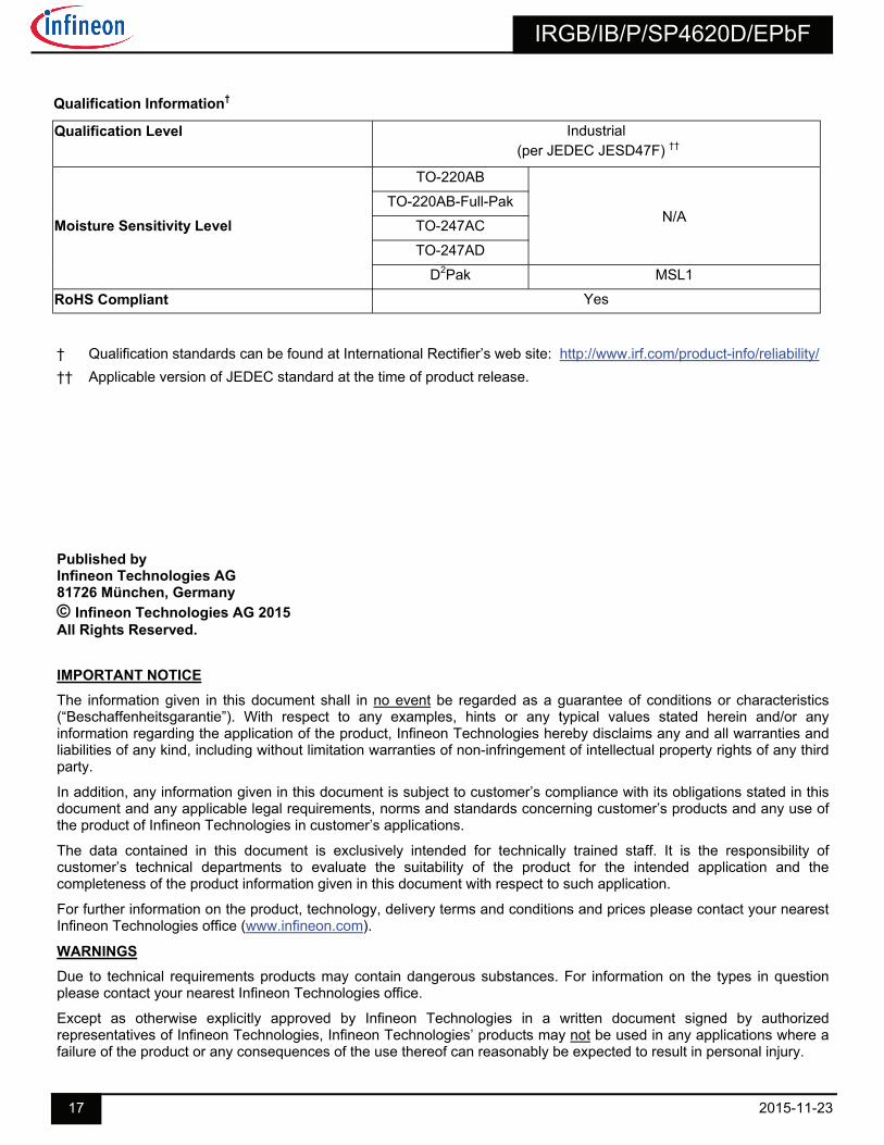
Qualification Information†
Qualification Level Industrial (per JEDEC JESD47F) ††
TO-220AB
TO-220AB-Full-Pak
Moisture Sensitivity Level TO-247AC
TO-247AD
D2Pak MSL1
RoHS Compliant Yes
N/A
† Qualification standards can be found at International Rectifier’s web site: http://www.irf.com/product-info/reliability/
†† Applicable version of JEDEC standard at the time of product release.
Published by Infineon Technologies AG 81726 München, Germany © Infineon Technologies AG 2015 All Rights Reserved.
IMPORTANT NOTICE
The information given in this document shall in no event be regarded as a guarantee of conditions or characteristics (“Beschaffenheitsgarantie”). With respect to any examples, hints or any typical values stated herein and/or any information regarding the application of the product, Infineon Technologies hereby disclaims any and all warranties and liabilities of any kind, including without limitation warranties of non-infringement of intellectual property rights of any third party.
In addition, any information given in this document is subject to customer’s compliance with its obligations stated in this document and any applicable legal requirements, norms and standards concerning customer’s products and any use of the product of Infineon Technologies in customer’s applications.
The data contained in this document is exclusively intended for technically trained staff. It is the responsibility of customer’s technical departments to evaluate the suitability of the product for the intended application and the completeness of the product information given in this document with respect to such application.
For further information on the product, technology, delivery terms and conditions and prices please contact your nearest Infineon Technologies office (www.infineon.com).
WARNINGS
Due to technical requirements products may contain dangerous substances. For information on the types in question please contact your nearest Infineon Technologies office.
Except as otherwise explicitly approved by Infineon Technologies in a written document signed by authorized representatives of Infineon Technologies, Infineon Technologies’ products may not be used in any applications where a failure of the product or any consequences of the use thereof can reasonably be expected to result in personal injury.