ir2166(s) & (pbf) - infineon technologies
TRANSCRIPT

Features• PFC, Ballast control and half-bridge driver in one IC
• Critical conduction mode boost type PFC
• No PFC current sense resistor required
• Programmable preheat frequency
• Programmable preheat time
• Programmable run frequency
• Programmable over-current protection
• Programmable end-of-life protection
Data Sheet No. PD60198 revF
IR2166(S) & (PbF)
PFC & BALLAST CONTROL IC
IR2166 Application Diagram
• Programmable dead time
• Internal ignition ramp
• Internal fault counter
• DC bus under-voltage reset
• Shutdown pin with hysteresis
• Internal 15.6V zener clamp diode on Vcc
• Micropower startup (150µA)
• Latch immunity and ESD protection
• Parts also available LEAD-FREE
Description
The IR2166 is a fully integrated, fully protected 600V ballast control IC designed todrive all types of fluorescent lamps. PFC circuitry operates in critical conduction modeand provides for high PF, low THD and DC Bus regulation. The IR2166 features in-clude programmable preheat and run frequencies, programmable preheat time, pro-grammable dead-time, programmable over-current protection, and programmable end-of-life protection. Comprehensive protection features such as protection from failure ofa lamp to strike, filament failures, end-of-life protection, DC bus undervoltage reset aswell as an automatic restart function, have been included in the design. The IR2166 isavailable in both 16-lead PDIP and 16-lead (narrow body) SOIC packages.
www.irf.com 1
Packages
*Please note that this data sheet contains advanced information that could change before the product is released to production.
16-Lead SOIC
(narrow body)
16-Lead PDIP
+ Rectified AC Line
- Rectified AC Line
R BUS
15
14
13
12
11IR21
66
COM
VCC
VB
VS
HO1
2
3
CPH
PFC
VBUS
4
5
7
RT
CT
RPH
6
7
8
ZX
COMP
10CS
LO
9SD/EOL
16
D BUS
D CP2
M3
+
C VDC
R VDC
C T
RT
RPH
C PH
CCOMP
CBUS
RGHSM1
R GPFC
LRESCBLOCK
CCS
RCS
R GLSM2
R 4
R 3
RSUPPLY
D BOOT
C BOOT
C SNUB
DCP1
R2
CVCC2CVCC1
+
CRES
C SD1 C SD2
R 5
R 6
R 7
R 8
D 1
D2 D3
R1DZCOMP
C EOL

IR2166 & (PbF)
2 www.irf.com
Absolute Maximum RatingsAbsolute maximum ratings indicate sustained limits beyond which damage to the device may occur. All voltage
parameters are absolute voltages referenced to COM, all currents are defined positive into any lead. The thermal
resistance and power dissipation ratings are measured under board mounted and still air conditions.
Note 1: This IC contains a zener clamp structure between the chip VCC and COM which has a nominal breakdown
voltage of 15.6V. Please note that this supply pin should not be driven by a DC, low impedance power source
greater than the VCLAMP specified in the Electrical Characteristics section.
Symbol Definition Min. Max. Units
VB High side floating supply voltage -0.3 625
VS High side floating supply offset voltage VB - 25 VB + 0.3
VHO High side floating output voltage VS - 0.3 VB + 0.3
VLO Low side output voltage -0.3 VCC + 0.3
VPFC PFC gate driver output voltage -0.3 VCC + 0.3
IOMAX Maximum allowable output current (HO, LO, PFC) -500 500
due to external power transistor miller effect
VBUS VBUS pin voltage -0.3 VCC + 0.3
VCT CT pin voltage -0.3 VCC + 0.3
ICPH CPH pin current -5 5
IRPH RPH pin current -5 5
VRPH RPH pin voltage -0.3 VCC + 0.3 V
IRT RT pin current -5 5 mA
VRT RT pin voltage -0.3 VCC + 0.3
VCS Current sense pin voltage -0.3 5.5
ICS Current sense pin current -5 5
ISD/EOL Shutdown pin current -5 5
ICC Supply current (Note 1) -20 20
IZX PFC inductor current, zero crossing detection input current -5 5
ICOMP PFC error compensation current -5 5
dV/dt Allowable offset voltage slew rate -50 50 V/ns
PD Package power dissipation @ TA ≤ +25°C (16-Pin PDIP) — 1.80
PD = (TJMAX-TA)/RthJA (16-Pin SOIC) — 1.40
RthJA Thermal resistance, junction to ambient (16-Pin PDIP) — 70
(16-Pin SOIC) — 86
TJ Junction temperature -55 150
TS Storage temperature -55 150
TL Lead temperature (soldering, 10 seconds) — 300
V
mA
mA
V
mA
V
W
oC/W
oC
IR2166 & (PbF)
www.irf.com 3
Note 2: Enough current should be supplied into the VCC lead to keep the internal 15.6V zener clamp diode on this lead
regulating its voltage, VCLAMP.
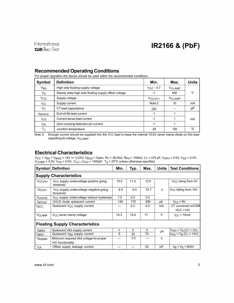
Recommended Operating ConditionsFor proper operation the device should be used within the recommended conditions.
Symbol Definition Min. Max. Units
VBS High side floating supply voltage VCC - 0.7 VCLAMP
VS Steady state high side floating supply offset voltage -1 600
VCC Supply voltage VCCUV+ VCLAMP
ICC Supply current Note 2 10 mA
CT CT lead capacitance 220 — pF
ISD/EOL End-of-life lead current -1 1
ICS Current sense lead current -1 1
IZX Zero crossing detection pin current -1 1
TJ Junction temperature -25 125 oC
V
mA
Electrical CharacteristicsVCC = VBS = VBIAS = 14V +/- 0.25V, VBUS = Open, RT = 39.0kΩ, RPH = 100kΩ, CT = 470 pF, VCPH = 0.0V, VSD = 0.0V,
VCOMP = 0.0V, VCS = 0.0V, CLO = CHO = 1000pF, TA = 25oC unless otherwise specified.
Symbol Definition Min. Typ. Max. Units Test Conditions
Supply Characteristics VCCUV+ VCC supply undervoltage positive going 10.0 11.5 12.5 VCC rising from 0V
threshold
VCCUV- VCC supply undervoltage negative going 8.5 9.5 10.7 VCC falling from 14V
threshold
VUVHYS VCC supply undervoltage lockout hysteresis 1.5 2.0 3.0
IQCCUV UVLO mode quiescent current 145 170 290 µA VCC = 8V
IQCC Quiescent VCC supply current — 2.3 4.0 mA CT connected toCOM
VCC =14V
VCLAMP VCC zener clamp voltage 14.3 15.6 17 V ICC = 10mA
IQBS0 Quiescent VBS supply current -1 0 5 VHO = VS (CT = 0V)
IQBS1 Quiescent VBS supply current 5 30 70 VHO = VB (CT = 14V)
VBSMIN Minimum required VBS voltage for proper — 2.5 — V
HO functionality
ILK Offset supply leakage current — — 50 µA VB = VS = 600V
µA
Floating Supply Characteristics
V

IR2166 & (PbF)
4 www.irf.com
Electrical Characteristics cont.VCC = VBS = VBIAS = 14V +/- 0.25V, VBUS = Open, RT = 39.0kΩ, RPH = 100kΩ, CT = 470 pF, VCPH = 0.0V, VSD = 0.0V,
VCOMP = 0.0V, VCS = 0.0V, CLO = CHO = 1000pF, TA = 25oC unless otherwise specified.
Symbol Definition Min. Typ. Max. Units Test Conditions
ICOMP Error amplifier output current sourcing 5 35 55 VCPH = 14V
SOURCE VBUS = 3.5V
ICOMP Error amplifier output current sinking -62 -30 -12 VCPH = 14V
SINK VBUS = 4.5V
VCOMPOH Error amplifier output voltage swing 10.5 13.5 14.5 VBUS = 3.0V
(high state)
VCOMPOL Error amplifier output voltage swing — 0.25 4 VBUS = 5.0V
(low state)
PFC Error Amplifier Characteristics
V
µA
VBUSOV Overvoltage comparator threshold 3.8 4.3 4.7 V VCOMP = 4.0V
VBUSOV Overvoltage comparator hysterisis 150 300 400 mV VCOMP = 4V
HYS
VVBUS VBUS internal reference voltage 3.7 4.0 4.2 V VCOMP = 4V
REG
PFC DC Bus Regulation
VZX ZX pin comparator threshold voltage 1.1 1.65 2 V VCOMP = 4V
VZXhys ZX pin comparator hysterisis 75 300 800 mV VCOMP = 4V
VZXclamp ZX pin clamp voltage (high state) 6.3 7.5 9.1 V IZX = 5mA
PFC Zero Current Detector
RPH CharacteristicsIRPHLK Open circuit RPH pin leakage current — 0.1 — µA
VRPHFLT Fault-mode RPH pin voltage — 0 — mV SD > 5.0V or CS >1.3V
PFC Watch-dogtWD Watch-dog pulse interval 90 400 824 µS ZX = 0V, VCOMP> =2V
Ballast Control Preheat CharacteristicsICPH CPH pin charging current 2.6 3.2 4.6 µA VCPH=5V,CT=0V, VBUS=0V
VCPHFLT Fault-mode CPH pin voltage — 0 — mV SD > 5.0V or CS >1.3V
Ballast Control Oscillator Characteristics
fosc Oscillator frequency 39 42 50 Run mode
73 78 84 Preheat mode
d Oscillator duty cycle — 50 — %
VCT+ Upper CT ramp voltage threshold 6.8 8.4 10.7
VCT- Lower CT ramp voltage threshold 1.8 4.6 5.6
VCTFLT Fault-mode CT lead voltage — 0 — SD > 5.0V or CS >1.3V
tDLO LO output deadtime 0.7 1.0 1.5
tDHO HO output deadtime 0.7 1.0 1.5
VVCC = 14V
usec CT = 470pF
kHz

IR2166 & (PbF)
www.irf.com 5
Electrical Characteristics cont.VCC = VBS = VBIAS = 14V +/- 0.25V, VBUS = Open, RT = 39.0kΩ, RPH = 100kΩ, CT = 470 pF, VCPH = 0.0V, VSD = 0.0V,
VCOMP = 0.0V VCS = 0.0V, CLO = CHO = 1000pF, TA = 25oC unless otherwise specified.
Symbol Definition Min. Typ. Max. Units Test Conditions
RT CharacteristicsIRTLK Open circuit RT pin leakage current — 0.1 — µA CT = 10V
VRTFLT Fault-mode RT pin voltage — 0 — mV SD > 5.0V or CS >1.3V
VOL Low-level output voltage — 0 100 Io = 0
VOH High-level output voltage — 0 100 VBIAS - Vo, Io = 0
tr Turn-on rise time — 110 210
tf Turn-off fall time — 55 160
I0+ HO, LO, PFC source current — 300 —
I0- HO, LO, PFC sink current — 400 —
Gate Driver Output Characteristics (HO, LO and PFC pins)
mV
nsecCHO = CLO = CPFC
= 1nF
mA
VSDTH+ Rising shutdown pin reset threshold voltage 4.5 5.2 5.6 V
VSDHYS Shutdown pin 5.0V threshold hysteresis 100 150 350 mV
VSDEOL+ Rising shutdown pin end-of-life threshold volt. 2.4 3.0 3.6
VSDEOL- Falling shutdown pin end-of-life threshold volt. 0.7 1.0 1.6
VCSTH+Over-current sense threshold voltage 0.91 1.2 1.3 VCPH>7.5V
#FAULT- Number of sequential over-current fault 25 75 90 Cycles VCPH>7.5V, CYCLES
cycles before IC shuts down CS > 1.3V
VBUSUV- The VBUS threshold below which the IC 2.6 3.0 3.3 shuts down
VCPH CPH pin end-of-life enable threshold 10.3 12 13.2
Protection Circuitry Characteristics
V VCPH>12V
V

IR2166 & (PbF)
6 www.irf.com
Block Diagram
PFCCOMP
ZX7.6V
1.0V
QS
R2 QR1
QS
R Q
VCC
RT
CPH
Vcc
CT
RPH
COM
R
VTH
R
3uAR
DriverLogic
Comp1
Schmitt1
SD/EOL
R
R
RDT3.0K
40K
S1
S2
S3
S4
QT
R Q
S6
QS
R2 QR1
VBUS
VB
HO
VS
LO
CS
High-Side
Driver
Low-Side
Driver
1.3V
Comp3
10
13
3
5
4
2
1
9
14
16
15
11
86
7
Under-VoltageDetect
WatchDog
Timer
12
SoftStart
Over-VoltageProtection
4.3V
FaultCounter
2.0V
1.0M
5.2V
1V
3V
CPH>12V
4.0V
3.0VQS
R Q
Under-VoltageReset
VCC
FaultLogic
7.6V
CPH>12V
GainOTA1

IR2166 & (PbF)
www.irf.com 7
State Diagram
VCC < 9.5V(VCC Fault or Power Down) orSD/EOL > 5.0V(Lamp Fault or Lamp Removal)
UVLO Mode1/2-Bridge OffIQCC ≅ 400µA
CPH = 0VCT = 0V (Oscillator Off)
PREHEAT Mode1/2-Bridge oscillating @ fPH
RPH // RTCPH Charging @ ICPH = 5 µA
PFC Enabled (High Gain)CS Enabled
Fault Counter Enabled
VCC > 11.5V (UV+) andSD/EOL < 5.0V
Power Turned On
FAULT ModeFault Latch Set
1/2-Bridge OffIQCC ≅ 180µA
CPH = 0VVCC = 15.6V
CT = 0V (Oscillator Off)
CS > 1.3V for 25 cycles(Failure to Strike Lamp)
SD/EOL > 5.0V(Lamp Removal) orVCC < 9.5V (UV-)(Power Turned Off)
CPH > (VCC - 4V)(End of PREHEAT Mode)
Ignition RampMode
RPH OpenfPH ramps to fRUN
CPH charging
CPH > (VCC - 2V)CS > 1.3V(Lamp Fault) orSD/EOL<1.0V or SD/EOL>3.0V(End-of-Life)
RUN ModeRPH = Open
1/2-Bridge Oscillating @fRUNEOL Thresholds Enabled PFC = Low Gain Mode
VBUS UV Threshold EnabledFault Counter Disabled
VBUS<3.0V
CS > 1.3V for 25 cycles
DischargeVCCto UVLO-

IR2166 & (PbF)
8 www.irf.com
Lead Assignments & Definitions
Pin # Symbol Description1
3
7654
2VBUS
ZXCOMP
CPH
CTRPHRT
Logic & Low-Side Gate Driver Supply
DC Bus Sensing Input
Minimum Frequency Timing ResistorPreheat Frequency Timing ResistorOscillator Timing Capacitor
Preheat Timing Capacitor
PFC Error Amplifier Compensation
PFCPFC Zero-Crossing Detection
89
11
15141312
10SD/EOL
VSVB
VCCCOMLOCS
PFC Gate Driver Output
IC Power & Signal Ground
Shut-Down/End of Life Sensing CircuitCurrent Sensing InputLow-Side Gate Driver Output
High Voltage Floating ReturnHigh-Side Gate Driver OutputHO
High-Side Gate Driver Floating Supply
16
15
14
13
12
11
IR21
66
COM
VCC
VB
VS
HO
1
2
3RT
CPH
VBUS
4
5
7
RPH
COMP
CT
6
7
8PFC
ZX
10CS
LO
9SD/EOL
16

IR2166 & (PbF)
www.irf.com 9
VCC
HO
LO
UVLO+15.6V
BALLAST TIMING DIAGRAMSNORMAL OPERATION
UVLO-
CPH
CS
PH
IGN RUN UVLOUVLO
1.3VOver-Current Threshold
FREQ
7.5V
VCC
fph
frun
RT
CT
LO
CS
HO
RPH
RT
CT
LO
CS
HO
RPH
RT
CT
LO
CS
HO
RPH

IR2166 & (PbF)
10 www.irf.com
VCC
HO
LO
UVLO+15.6V
BALLAST TIMINGDIAGRAMS
FAULT CONDITION
UVLO-
CPH
CS
PH
IGN RUN UVLOUVLO
1.3V
FREQ
7.5V
VCC
f ph
frun
FAULT
PH
IGN
SD > 5.1V
SD
RT
CT
LO
CS
HO
RPH
RT
CT
LO
CS
HO
RPH
RT
CT
LO
CS
HO
RPH

IR2166 & (PbF)
www.irf.com 11
1000
10000
100000
1000000
5 25 45 65 85
RT(KΩ)
Freq
uenc
y (K
Hz)
Graph 2. CT vs Dead Time
Graph 3: CT+, CT- vs TEMP Graph 4: Frequency vs RT
Graph 1. VCCUV+, VCCUV- vs TEMP
0
1
2
3
4
5
6
7
8
9
-25 0 25 50 75 100 125
Temperature (°C)
CT
(V)
CT+
CT-
0
2
4
6
8
10
12
14
-25 0 25 50 75 100 125
Temperature (°C)
VCC
(V)
UVLO+
UVLO-
0
200
400
600
800
1000
1200
1400
1600
0 0.5 1 1.5 2 2.5 3
DeadTime(µS)
CT
(pF)

IR2166 & (PbF)
12 www.irf.com
0
1
2
3
4
5
6
7
8
40 80 120 160 200
FREQUENCY (KHz)
ICC
(mA)
-1.5
-1
-0.5
0
0.5
1
1.5
2
2.5
3
3.5
0 3 6 9 12 15
VCPH (V)
ICPH
(mA)
0
10
20
30
40
50
-25 0 25 50 75 100 125
Temperature (°C)
ILK
(A)
Graph 5: ICC vs Frequency Graph 6: ICPH vs VCPH
Graph 7. ILK vs TEMP Graph 8: ZX+, ZX- vs TEMP
0
0.5
1
1.5
2
2.5
-25 0 25 50 75 100 125
Temperature (°C)
ZX T
hres
hold
& H
YS.(V
)
ZX+
ZX-
HYS

IR2166 & (PbF)
www.irf.com 13
275
285
295
305
315
325
-25 0 25 50 75 100 125
Temperature (°C)
IZX
(ZXI
nput
Bia
s) (
A)
6
6.5
7
7.5
8
8.5
9
-25 0 25 50 75 100 125
Temperature (°C)
Graph 9: IZX (ZX Input Bias) vs TEMP Graph 10: VZX (ZX Clamp Voltage) vs TEMP
3
3.5
4
4.5
5
-25 0 25 50 75 100 125
Temperature (°C)
3
3.5
4
4.5
5
-25 0 25 50 75 100 125
Temperature (°C)
VBUS+
VBUS-
Graph 11: VBUS Sense Thresh vs TEMP Graph 12: VBUS+, VBUS- vs TEMP

IR2166 & (PbF)
14 www.irf.com
53
55
57
59
61
63
-25 0 25 50 75 100 125
Temperature (°C)
FREQ
(KH
z)
1.5
1.7
1.9
2.1
2.3
2.5
-25 0 25 50 75 100 125
Temperature (°C)
t DEA
D (
S) tDEAD HO
tDEAD LO
Graph 13: PFC Trise, Tfall vs TEMP Graph 14: Frequency vs TEMP
Graph 15: tDEAD HO, tDEAD LO vs TEMP
0
25
50
75
100
125
150
175
200
-25 0 25 50 75 100 125
Temperature (°C)
t RIS
E, t F
ALL
(nS)
tRISE
tFALL
Graph 16: tRISE, tFALL vs TEMP
0
25
50
75
100
125
150
-25 0 25 50 75 100 125
Temperature (°C)
PFC
Tris
e, T
fall
(nS)
Trise
Tfall

IR2166 & (PbF)
www.irf.com 15
Graph 17: CS Pulses vs TEMP
0
1
2
3
4
5
-25 0 25 50 75 100 125
Temperature (°C)
CS
Thre
shol
d (V
)
Graph 18: CS Threshold vs TEMP
Graph 20: SD+, SD- vs TEMP
0
0.5
1
1.5
2
2.5
3
3.5
-25 0 25 50 75 100 125
Temperature (°C)
VSD
/EO
L (V
)
Graph 19: EOL+,EOL- vs TEMP
EOL+
EOL-
4
4.5
5
5.5
6
-25 0 25 50 75 100 125
Temperature (°C)
VSD
/EO
L (V
)
SD+
SD-
0
10
20
30
40
50
-25 0 25 50 75 100 125
Temperature (°C)
# C
S Pu
lses

IR2166 & (PbF)
16 www.irf.com
10
11
12
13
14
15
-25 0 25 50 75 100 125
Temperature (°C)
VCPH
(EO
L/R
UN
) Thr
esho
ld (V
)
Graph 21: VCPH (EOL/RUN) Threshold vs TEMP
0
2
4
6
8
10
12
14
16
0 5 10 15 20
PFC ON TIME (µS)
VC
OM
P (V
)
Graph 23: VCOMP vs PFC ON TIME
-10
0
10
20
30
40
50
60
70
80
90
0 3 6 9 12 15
VBS (V)
I QBS
(A)
0
0.5
1
1.5
2
2.5
3
8 9 10 11 12 13
VCC (V)
IQC
C (m
A)
Graph 22: IQCC vs VCC UVLO Hysteresis
Graph 24: IQBS(1) vs VCC vs Temp

IR2166 & (PbF)
www.irf.com 17
0
4
8
12
16
20
0 5 10 15 20
VCC (V)
IQC
C (m
A)
-252575125
Graph 25. IQCC vs VCC vs Temp
0
0.05
0.1
0.15
0.2
0.25
0.3
0 3 6 9 12 15
VCC (V)
IQC
C (m
A)
-252575125
Graph 27. IQCC vs VCC vs Temp Micropower Startup Mode
0
4
8
12
16
20
15 15.5 16 16.5
VCC (V)
I QC
C (m
A)
-252575125
Graph 26. IQCC vs VCC vs Temp Internal Zener Diode Curve
Graph 28: IQCC vs VCC vs Temp VCCUV+
0
0.5
1
1.5
2
2.5
10 10.5 11 11.5 12 12.5 13V C C (V)
-252575125

IR2166 & (PbF)
18 www.irf.com
0
0.5
1
1.5
2
2.5
3
8.5 9 9.5 10 10.5
VCC (V)
I QC
C (
A)
-252575125
Graph 29: IQCC vs VCC vs Temp VCCUV-
IR2166 & (PbF)
www.irf.com 19
IR2166
LO
COM
VB
VS
HO
VBUS(+)
VBUS(-)
VCC
D BOOT
C BOOT
16
15
14
13
12
11 M2
M1
C VCC
R SUPPLY
D CP1
D CP2
Half-BridgeOutput
RCS
C SNUB
I. Ballast Section
Functional Description
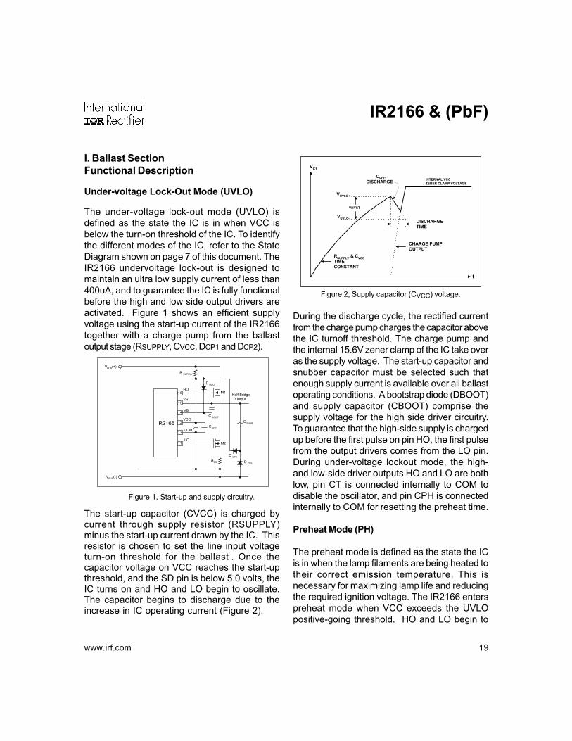
Under-voltage Lock-Out Mode (UVLO)
The under-voltage lock-out mode (UVLO) is
defined as the state the IC is in when VCC is
below the turn-on threshold of the IC. To identify
the different modes of the IC, refer to the State
Diagram shown on page 7 of this document. The
IR2166 undervoltage lock-out is designed to
maintain an ultra low supply current of less than
400uA, and to guarantee the IC is fully functional
before the high and low side output drivers are
activated. Figure 1 shows an efficient supply
voltage using the start-up current of the IR2166
together with a charge pump from the ballast
output stage (RSUPPLY, CVCC, DCP1 and DCP2).
Figure 1, Start-up and supply circuitry.
The start-up capacitor (CVCC) is charged bycurrent through supply resistor (RSUPPLY)minus the start-up current drawn by the IC. Thisresistor is chosen to set the line input voltageturn-on threshold for the ballast . Once thecapacitor voltage on VCC reaches the start-upthreshold, and the SD pin is below 5.0 volts, theIC turns on and HO and LO begin to oscillate.The capacitor begins to discharge due to theincrease in IC operating current (Figure 2).
DISCHARGETIME
INTERNAL VCCZENER CLAMP VOLTAGE
VHYST
VUVLO+
VUVLO-
CHARGE PUMPOUTPUT
t
VC1
RSUPPLY & CVCCTIMECONSTANT
CVCCDISCHARGE
Figure 2, Supply capacitor (CVCC) voltage.
During the discharge cycle, the rectified current
from the charge pump charges the capacitor above
the IC turnoff threshold. The charge pump and
the internal 15.6V zener clamp of the IC take over
as the supply voltage. The start-up capacitor and
snubber capacitor must be selected such that
enough supply current is available over all ballast
operating conditions. A bootstrap diode (DBOOT)
and supply capacitor (CBOOT) comprise the
supply voltage for the high side driver circuitry.
To guarantee that the high-side supply is charged
up before the first pulse on pin HO, the first pulse
from the output drivers comes from the LO pin.
During under-voltage lockout mode, the high-
and low-side driver outputs HO and LO are both
low, pin CT is connected internally to COM to
disable the oscillator, and pin CPH is connected
internally to COM for resetting the preheat time.
Preheat Mode (PH)
The preheat mode is defined as the state the IC
is in when the lamp filaments are being heated to
their correct emission temperature. This is
necessary for maximizing lamp life and reducing
the required ignition voltage. The IR2166 enters
preheat mode when VCC exceeds the UVLO
positive-going threshold. HO and LO begin to
IR2166 & (PbF)
20 www.irf.com
4
3
3uA
5
2CPH
CT
RPH
RT
11
12 COM
LOM2
RCS
OSC 16HO
M1
15VS
CCPH
CT
Half-BridgeOutput
ILOAD
(+)
VBUS (-)
LoadReturn
Half-BridgeDriver
IR2166
1.3V
S1
S4
Comp 4
10
13VCC
CS
R1
CCS
S3
FaultLogic
VBUS
RT
RPH
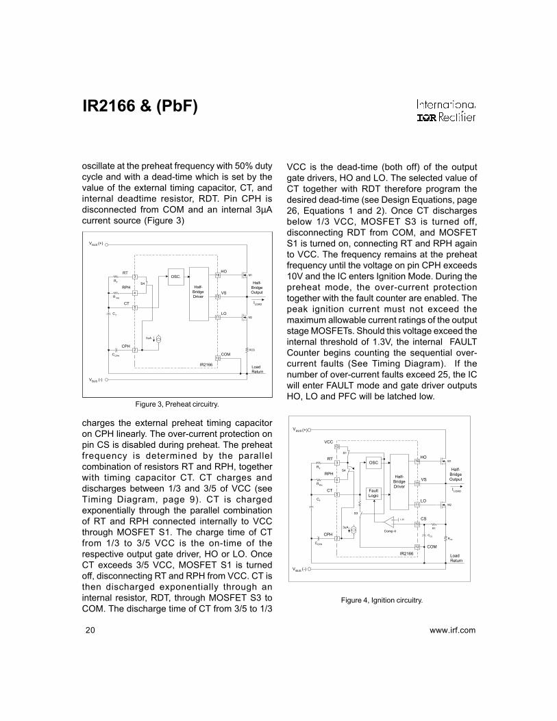
oscillate at the preheat frequency with 50% duty
cycle and with a dead-time which is set by the
value of the external timing capacitor, CT, and
internal deadtime resistor, RDT. Pin CPH is
disconnected from COM and an internal 3µA
current source (Figure 3)
Figure 3, Preheat circuitry.
charges the external preheat timing capacitor
on CPH linearly. The over-current protection on
pin CS is disabled during preheat. The preheat
frequency is determined by the parallel
combination of resistors RT and RPH, together
with timing capacitor CT. CT charges and
discharges between 1/3 and 3/5 of VCC (see
Timing Diagram, page 9). CT is charged
exponentially through the parallel combination
of RT and RPH connected internally to VCC
through MOSFET S1. The charge time of CT
from 1/3 to 3/5 VCC is the on-time of the
respective output gate driver, HO or LO. Once
CT exceeds 3/5 VCC, MOSFET S1 is turned
off, disconnecting RT and RPH from VCC. CT is
then discharged exponentially through an
internal resistor, RDT, through MOSFET S3 to
COM. The discharge time of CT from 3/5 to 1/3
VCC is the dead-time (both off) of the output
gate drivers, HO and LO. The selected value of
CT together with RDT therefore program the
desired dead-time (see Design Equations, page
26, Equations 1 and 2). Once CT discharges
below 1/3 VCC, MOSFET S3 is turned off,
disconnecting RDT from COM, and MOSFET
S1 is turned on, connecting RT and RPH again
to VCC. The frequency remains at the preheat
frequency until the voltage on pin CPH exceeds
10V and the IC enters Ignition Mode. During the
preheat mode, the over-current protection
together with the fault counter are enabled. The
peak ignition current must not exceed the
maximum allowable current ratings of the output
stage MOSFETs. Should this voltage exceed the
internal threshold of 1.3V, the internal FAULT
Counter begins counting the sequential over-
current faults (See Timing Diagram). If the
number of over-current faults exceed 25, the IC
will enter FAULT mode and gate driver outputs
HO, LO and PFC will be latched low.
Figure 4, Ignition circuitry.
4
3
3uA
5
2CPH
CT
RPH
RT
11
12COM
LOM2
RCS
OSC. 16HO
M1
15VS
RT
CCPH
Half-BridgeOutput
ILOAD
VBUS (+)
VBUS (-)
LoadReturn
Half-BridgeDriver
IR2166
S4
R PH
CT

IR2166 & (PbF)
www.irf.com 21
Ignition Mode (IGN)
The ignition mode is defined as the state the IC
is in when a high voltage is being established
across the lamp necessary for igniting the lamp.
The IR2166 enters ignition mode when the
voltage on pin CPH exceeds 10V.
Pin CPH is connected internally to the gate of a
P-channel MOSFET (S4) (see Figure 4) that
connects pin RPH with pin RT. As pin CPH
exceeds 10V, the gate-to-source voltage of
MOSFET S4 begins to fall below the turn-on
threshold of S4. As pin CPH continues to ramp
towards VCC, switch S4 turns off slowly. This
results in resistor RPH being disconnected
smoothly from resistor RT, which causes the
operating frequency to ramp smoothly from the
preheat frequency, through the ignition frequency,
to the final run frequency. The over-current
threshold on pin CS will protect the ballast
against a non-strike or open-filament lamp fault
condition. The voltage on pin CS is defined by
the lower half-bridge MOSFET current flowing
through the external current sensing resistor
RCS. The resistor RCS therefore programs the
maximum allowable peak ignition current (and
therefore peak ignition voltage) of the ballast
output stage. If the number of over current pulses
exceed 25, the IC will enter fault mode and gate
driver outputs HO, LO and PFC will be latched
low.
Run Mode (RUN)
Once the lamp has successfully ignited, the
ballast enters run mode. The run mode is defined
as the state the IC is in when the lamp arc is
established and the lamp is being driven to a
given power level. The run mode oscillating
frequency is determined by the timing resistor
RT and timing capacitor CT (see Design
Equations, page 26, Equations 3 and 4). Should
hard-switching occur at the half-bridge at any
time due to an open-filament or lamp removal,
the voltage across the current sensing resistor,
RCS, will exceed the internal threshold of 1.3 volts
and the IC will enter FAULT mode and gate driver
outputs HO, LO and PFC will be latched low.
DC Bus Under-voltage Reset
Should the DC bus decrease too low during a
brownout line condition or overload condition,
the resonant output stage to the lamp can shift
near or below resonance. This can produce
hard-switching at the half-bridge which can
damage the half-bridge switches or, the DC bus
can decrease too far and the lamp can
extinguish. To protect against this, the VBUS pin
includes a 3.0V under-voltage threshold. Should
the voltage at the VBUS pin decrease below 3.0V,
VCC will be discharged to the UVLO- threshold
and all gate driver outputs will be latched low.
For proper ballast design, the designer should
design the PFC section such that the DC bus
does not drop until the AC line input voltage falls
below the rated input voltage of the ballast (See
PFC section). When correctly designed, the
voltage measured at the VBUS pin will decrease
below the internal 3.0V threshold and the ballast
will turn off cleanly. The pull-up resistor to VCC
(RSUPPLY) will then turn the ballast on again
with the AC input line voltage increasing to the
minimum specified value causing VCC to exceed
UVLO+.
RSUPPLY should be set to turn the ballast on at
the minimum specified ballast input voltage. The
PFC should then be designed such that the DC
bus decreases at an input line voltage that is

IR2166 & (PbF)
22 www.irf.com
lower than the minimum specified ballast input
voltage. This hysteresis will result in clean turn-
on and turnoff of the ballast.
CS and EOL Fault Mode (FAULT)
Should the voltage at the SD/EOL pin exceed 3V
or decrease below 1V during RUN mode, the IC
enters fault mode and all gate driver outputs, HO,
LO and PFC, are latched off in the 'low' state.
CPH is discharged to COM for resetting the
preheat time, and CT is discharged to COM for
disabling the oscillator. To exit fault mode, VCC
must be recycled back below the UVLO negative-
going turn-off threshold, or, the shutdown pin, SD,
must be pulled above 5.2 volts. Either of these
will force the IC to enter UVLO mode (see State
Diagram, page 7). Once VCC is above the turn-
on threshold and SD is below 5.0 volts, the IC
will begin oscillating again in the preheat mode.
The current sense function will force the IC to
enter FAULT mode only after the voltage at the
current sense pin has been pulsed about 25 times
with a voltage greater than 1.3 volts during preheat
and ignition modes only. These over-currents must
occur during the on-time of LO. During run mode,
a single pulse on the CS pin above 1.3V will force
the IC to enter FAULT mode.
II. PFC Section Functional Description
In most electronic ballasts it is necessary to
have the circuit act as a pure resistive load to
the AC input line voltage. The degree to which
the circuit matches a pure resistor is measured
by the phase shift between the input voltage
and input current and how well the shape of the
input current waveform matches the shape of
the sinusoidal input voltage. The cosine of the
phase angle between the input voltage and input
current is defined as the power factor (PF), and
how well the shape of the input current waveform
matches the shape of the input voltage is
determined by the total harmonic distortion
(THD). A power factor of 1.0 (maximum)
corresponds to zero phase shift and a THD of
0% represents a pure sinewave (no distortion).
For this reason it is desirable to have a high PF
and a low THD. To achieve this, the IR2166
includes an active power factor correction (PFC)
circuit which, for an AC line input voltage,
produces an AC line input current. The control
method implemented in the IR2166 is for a boost-
type converter (Figure 6) running in critical-
conduction mode (CCM). This means that during
each switching cycle of the PFC MOSFET, the
circuit waits until the inductor current discharges
to zero before turning the PFC MOSFET on again.
The PFC MOSFET is turned on and off at a
much higher frequency (>10KHz) than the line
input frequency (50 to 60Hz).LO
CS
25 Pulses
Run Mode Fault Mode
2.0V
Figure 5: FAULT counter during preheat and ignition
CBUS
+
(+)
(-)
MPFC
LPFC DPFCDC Bus
Figure 6: Boost-type PFC circuit

IR2166 & (PbF)
www.irf.com 23
When the switch MPFC is turned on, the inductor
LPFC is connected between the rectified line
input (+) and (-) causing the current in LPFC to
charge up linearly. When MPFC is turned off,
LPFC is connected between the rectified line
input (+) and the DC bus capacitor CBUS
(through diode DPFC) and the stored current in
LPFC flows into CBUS. As MPFC is turned on
and off at a high-frequency, the voltage on CBUS
charges up to a specified voltage. The feedback
loop of the IR2166 regulates this voltage to a
fixed value by continuously monitoring the DC
voltage and adjusting the on-time of MPFC
accordingly. For an increasing DC bus the on-
time is decreased, and for a decreasing DC bus
the on-time is increased. This negative feedback
control is performed with a slow loop speed and
a low loop gain such that the average inductor
current smoothly follows the low-frequency line
input voltage for high power factor and low THD.
The on-time of MPFC therefore appears to be
fixed (with an additional modulation to be
discussed later) over several cycles of the line
voltage. With a fixed on-time, and an off-time
determined by the inductor current discharging
to zero, the result is a system where the
switching frequency is free-running and
constantly changing from a high frequency near
the zero crossing of the AC input line voltage,
to a lower frequency at the peaks (Figure 7).
Figure 7: Sinusoidal line input voltage (solid line), triangular
PFC Inductor current and smoothed sinusoidal line input
current (dashed line) over one half-cycle of the line input
voltage.
When the line input voltage is low (near the zero
crossing), the inductor current will charge up to
a small amount and the discharge time will be
fast resulting in a high switching frequency.
When the input line voltage is high (near the
peak), the inductor current will charge up to a
higher amount and the discharge time will be
longer giving a lower switching frequency. The
triangular PFC inductor current is then smoothed
by the EMI filter to produce a sinusoidal line
input current.
The PFC control circuit of the IR2166 (Figure 8)
only requires four control pins: VBUS, COMP,
ZX and PFC. The VBUS pin is for sensing the
DC bus voltage (via an external resistor voltage
divider), the COMP pin programs the on-time of
MPFC and the speed of the feedback loop, the
ZX pin detects when the inductor current
discharges to zero (via a secondary winding
from the PFC inductor), and the PFC pin is the
low-side gate driver output for MPFC.
V, I
t

IR2166 & (PbF)
24 www.irf.com
RVBUS1
RVBUSCCOMP
LPFC
MPFCRPFC
DFPC
CBUS
(+)
(-)
RZX
PFCControl
VBUS
COMP PFC
ZX
COM
DCOMP
Figure 8:IR2166 simplified PFC control circuit
The VBUS pin is regulated against a fixed
internal 4V reference voltage for regulating the
DC bus voltage (Figure 9). The feedback loop
is performed by an operational transconductance
amplifier (OTA) that sinks or sources a current
to the external capacitor at the COMP pin. The
resulting voltage on the COMP pin sets the
threshold for the charging of the internal timing
capacitor (C1) and therefore programs the on-
time of MPFC. During preheat and ignition
modes of the ballast section, the gain of the
OTA is set to a high level to raise the DC bus
level quickly. When the voltage on the VBUS pin
exceeds 3V, the gain is set to a low level to
reduce overshoot. When the voltage on the VBUS
pin exceeds 4V, the gain is set to a high level
again to minimize the transient on the DC bus
which can occur during ignition. During run
mode, the gain is then decreased to a lower
level necessary for achieving high power factor
and low THD.
Figure 9: IR2166 detailed PFC control circuit
The off-time of MPFC is determined by the time
it takes the LPFC current to discharge to zero.
This zero current level is detected by a
secondary winding on LPFC which is connected
to the ZX pin. A positive-going edge exceeding
the internal 2V threshold signals the beginning
of the off-time. A negative-going edge on the
ZX pin falling below 1.7V will occur when the
LPFC current discharges to zero which signals
the end of the off-time and MPFC is turned on
again (Figure 10). The cycle repeats itself
indefinitely until the PFC section is disabled due
to a fault detected by the ballast section (Fault
Mode), an over-voltage or under-voltage
condition on the DC bus, or, the negative
transition of ZX pin voltage does not occur.
Should the negative edge on the ZX pin not occur,
MPFC will remain off until the watch-dog timer
forces a turn-on of MPFC for an on-time duration
programmed by the voltage on the COMP pin.
The watch-dog pulses occur every 400µs
indefinitely until a correct positive- and negative-
going signal is detected on the ZX pin and normal
PFC operation is resumed.
7
6
1
QS
R Q
2.0V
VBUS
COMP
ZX7.6V
4.0V
GAINOTA1
4.3V 8 PFC
QS
R2 QR1
COMP3
COMP4
COMP5RS3
RS4
VCC
Run Mode Signal Fault Mode Signal
M1
WATCHDOG
TIMERM2C1
3.0V
DischargeVCC toUVLO-
COMP2

IR2166 & (PbF)
www.irf.com 25
0
0
0
ILPFC
PFCpin
ZXpin
Figure 10: LPFC current, PFC pin and ZX pin timing
diagram.
On-time Modulation
A fixed on-time of MPFC over an entire cycle of
the line input voltage produces a peak inductor
current which naturally follows the sinusoidal
shape of the line input voltage. The smoothed
averaged line input current is in phase with the
line input voltage for high power factor but the
total harmonic distortion (THD), as well as the
individual higher harmonics, of the current can
still be too high. This is mostly due to cross-
over distortion of the line current near the zero-
crossings of the line input voltage. To achieve
low harmonics which are acceptable to
international standard organizations and general
market requirements, an additional on-time
modulation circuit has been added to the PFC
control. This circuit dynamically increases the
on-time of MPFC as the line input voltage nears
the zero-crossings (Figure 11). This causes the
peak LPFC current, and therefore the smoothed
line input current, to increase slightly higher near
the zero-crossings of the line input voltage. This
reduces the amount of cross-over distortion in
the line input current which reduces the THD
and higher harmonics to low levels.
0
0
ILPFC
PFCpin
near peak region ofrectified AC line
near zero-crossing regionof rectified AC line
Figure 11: On-time modulation near the zero-crossings.
Over-voltage Protection (OVP)
Should over-voltage occur on the DC bus
causing the VBUS pin to exceed the internal 4.3V
threshold, the PFC output is disabled (set to a
logic 'low'). When the DC bus decreases again
causing the VBUS pin to decrease below the
internal 4V threshold, a watch-dog pulse is forced
on the PFC pin and normal PFC operation is
resumed.
Under-voltage Reset (UVR)
When the line input voltage is decreased,
interrupted or a brown-out condition occurs, the
PFC feedback loop causes the on-time of MPFC

IR2166 & (PbF)
26 www.irf.com
to increase in order to keep the DC bus constant.
Should the on-time increase too far, the resulting
peak currents in LPFC can exceed the saturation
current limit of LPFC. LPFC will then saturate
and very high peak currents and di/dt levels will
occur. To prevent this, the maximum on-time is
limited by limiting the maximum voltage on the
COMP pin with an external zener diode DCOMP
(Figure 8). As the line input voltage decreases,
the COMP pin voltage and therefore the on-time
will eventually limit. The PFC can no longer
supply enough current to keep the DC bus fixed
for the given load power and the DC bus will
begin to drop. Decreasing the line input voltage
further will cause the VBUS pin to eventually
decrease below the internal 3V threshold (Figure
9). When this occurs, VCC is discharged
internally to UVLO-, the IR2166 enters UVLO
mode and both the PFC and ballast sections
are disabled (see State Diagram). The start-up
supply resistor to VCC, together with the micro-
power start-up current of the IR2166, determine
the line input turn-on voltage. This should be
set such that the ballast turns on at a line voltage
level above the under-voltage turn-off level. It
is the correct selection of the value of the supply
resistor to VCC and the zener diode on the
COMP pin that correctly program the on and off
line input voltage thresholds for the ballast. With
these thresholds correctly set, the ballast will
turn off due to the 3V under-voltage threshold
on the VBUS pin, and on again at a higher line
input voltage (hysterisis) due to the supply
resistor to VCC. This hysterisis will result in a
proper reset of the ballast without flickering of
the lamp, bouncing of the DC bus or re-ignition
of the lamp when the DC bus is too low.
PFC Over-Current Protection (optional)
In case of fast on/off interruptions of the mains inputvoltage or during normal lamp ignition, the DC bus
voltage level can decrease below the instantaneous
rectified line voltage. Should this occur, the PFC
inductor current and PFC MOSFET current can
increase to high levels causing the PFC inductor to
saturate and/or the PFC MOSFET to become
damaged. During fast on/off interruptions of the input
mains voltage, the DC bus can drop during the time
when the mains voltage is interrupted (off). Since
VCC is still above UVLO-, the IC will continue to
operate and will increase the COMP pin voltage to
increase the PFC MOSFET on-time due to the
dropping of the DC bus. When the mains voltage
returns again quickly, (before VCC reaches UVLO-
), the on-time of the PFC MOSFET is too long for
the given mains voltage level resulting in high PFC
inductor and MOSFET currents that can saturate
the inductor and/or damage the PFC MOSFET
(Figure 12).
Figure 12, High PFC inductor current during fast mains
on/off (upper trace: DC Bus, 100V/div; middle trace:
AC line input voltage, 100V/div; lower trace: PFC
inductor current 1A/div).

IR2166 & (PbF)
www.irf.com 27
During lamp ignition, the DC bus can drop below
the rectified AC line voltage causing current to
conduct directly from the output of the rectifier,
through the PFC inductor and diode, to the DC
bus capacitor. This results in a low-frequency offset
of current in the PFC inductor. Since the zero-
crossing detection circuit only detects the high-
frequency zero-crossing of the inductor current,
the PFC MOSFET will turn on again each cycle
before the inductor current has reached zero. This
causes the PFC to work in a continuous conduction
mode and the sum of the low-frequency and high-
frequency components of current can saturate the
PFC inductor and/or damage the PFC MOSFET.
To protect against these conditions, a current
sense resistor (RS) can be inserted between the
source on the PFC MOSFET and ground, and a
diode (D4) connected from the top of this current-
sensing resistor to the VBUS pin (Figure 13).
13, External over-current protection circuit
Should high currents occur, the voltage across
the current-sensing resistor (RS) will exceed the
4.3V over-voltage protection threshold at the VBUS
pin and the PFC MOSFET will turn off safely
limiting the current. The watch-dog timer will then
RectifiedAC line
15
14
13
12
11
IR21
66
COM
VCC
VB
VS
HO
1
2
3RT
CPH
VBUS
4
5
7
RPH
COMP
CT
6
7
8PFC
ZX
10CS
LO
9SD/EOL
16
RS
D4
1N4148
1Ω
HighCurrentGround
DeviceGround
restart the PFC as normal (Figure 14). The current
sensing resistor value should be selected such
that the over-current protection does not false trip
during normal operation over the entire line voltage
range and load range. A current-sensing resistor
value, for example, of 1.0 W will set the over-
current protection threshold to about 5 A peak.
Figure 14, PFC inductor current limited using over-
current protection circuit (upper trace: DC Bus,
100V/div; middle trace: AC line input voltage, 100V/div; lower trace: PFC inductor current 1A/div).
The effect that these line and load conditions have
on the performance of the ballast depends on the
saturation level of the PFC inductor, the selection
of the PFC MOSFET, the DC bus capacitor value,
the maximum on-time limit set by DZCOMP, and,
how fast VCC decreases below UVLO- when the
DC bus drops during ignition (the 3V reset on the
VBUS pin does not become active until RUN mode).
For these reasons, the ballast designer should
perform these mains interrupt and ignition tests
carefully to determine the robustness of their final
design and to decide if this additional over-current
protection circuit is necessary.

IR2166 & (PbF)
28 www.irf.com
Step 3: Program Preheat Frequency
The preheat frequency is programmed with
timing resistors RT and RPH, and timing
capacitor CT. The timing resistors are
connected in parallel internally for the duration
of the preheat time. The preheat frequency is
therefore given as:
+
+⋅⋅
⋅⋅=
147551.0
2
1
PHT
PHTT
PH
RRRR
Cf
[Hertz] (5)
or
−
⋅⋅−
⋅
−
⋅⋅=
289202.1
1
289202.1
1
PHTT
TPHT
PH
fCR
RfC
R[Ohms] (6)
Step 4: Program Preheat Time
The preheat time is defined by the time it takes
for the capacitor on pin CPH to charge up to
10 volts. An internal current source of 3uA flows
out of pin CPH. The preheat time is therefore
given as:
633.3 eCt PHPH ⋅= [Seconds] (7)
or
63.0 −⋅= etC PHPH [Farads] (8)
Ballast Design Equations
Note: The results from the following design
equations can differ slightly from experimental
measurements due to IC tolerances, component
tolerances, and oscillator over- and undershoot
due to internal comparator response time.
Step 1: Program Dead-time
The dead-time between the gate driver outputs
HO and LO is programmed with timing capacitor
CT and an internal dead-time resistor RDT. The
dead-time is the discharge time of capacitor CT
from 3/5VCC to 1/3VCC and is given as:
1475⋅= TDT Ct [Seconds] (1)
or
1475DT
Tt
C = [Farads] (2)
Step 2: Program Run Frequency
The final run frequency is programmed with
timing resistor RT and timing capacitor CT. The
charge time of capacitor CT from 1/3VCC to
3/5VCC determines the on-time of HO and LO
gate driver outputs. The run frequency is
therefore given as:
)147551.0(21
+⋅⋅=
TTRUN RCf [Hertz] (3)
or
289202.1
1 −⋅⋅
=RUNT
T fCR [Ohms] (4)

IR2166 & (PbF)
www.irf.com 29
Step 5: Program Maximum Ignition Current
The maximum ignition current is programmed
with the external resistor RCS and an internal
threshold of 1.3 volts. This threshold determines
the over-current limit of the ballast, which can
be exceeded when the frequency ramps down
towards resonance during ignition and the lamp
does not ignite. The maximum ignition current
is given as:
CSIGN RI 3.1= [Amps Peak] (9)
or
IGNCS IR 3.1=
[Ohms] (10)

IR2166 & (PbF)
30 www.irf.com
P F C D e s ig n E q u a tio n s
S te p 1 : C a lc u la te P F C in d u c to r va lu e :
VBUSPfVACVACVBUSL
OUTMIN
MINMINPFC ⋅⋅⋅
⋅⋅⋅−=2
)2( 2 η [H enries] (1 )
w here , VBUS = D C b u s vo ltag e
MINVAC = M in im u m rm s A C in p u t vo lta g e
η = P F C e ffic ie nc y (typ ic a lly 0 .9 5 )
MINf = M in im u m P F C s w itc h in g fre q u e n c y a t m in im u m A C in p u t vo lta ge
OUTP = B a lla s t o u tp u t p o w e r
S te p 2 : C a lc u la te p e a k P F C ind u c to r c u rre n t:
η⋅
⋅⋅=
MIN
OUTPK VAC
Pi 22 [A m p s P eak] (2 )
N o te : T h e P F C in d u c to r m u s t n o t s a tu ra te a t PKi o ve r th e s pe c ifie d b a lla s t o p e ra tin g te m p e ra tu re ra n g e . P ro p e r c o re s iz in g a n d a ir-g a p p in g s h o u ld b e c o n s id e re d in th e in d u c to r d e s ig n .
S te p 3 : C a lc u la te m a xim u m o n-tim e :
η⋅
⋅⋅= 2
2
MIN
PFCOUTON VAC
LPt
MAX [S eco nd s] (3 )
S te p 4 : C a lc u la te m a xim u m C O M P vo lta g e :
69.0 −
=E
tV MAXON
MAXCOMP [V o lts] (4 )
S te p 5 : S e lec t ze n e r d io d e D C O M P va lu e :
COMPD zene r vo ltage ≈ MAXCOMPV [V o lts] (5 )
S te p 6 : C a lc u la te re s is to r R S U P P L Y va lu e :
IQCCUV
VACR PK
MINSUPPLY
10+= [O hm s] (6 )

IR2166 & (PbF)
www.irf.com 31
Case outline
16 Lead PDIP01-6015
01-3065 00 (MS-001A)
16 Lead SOIC (narrow body)01-6018
01-3064 00 (MS-012AC)

IR2166 & (PbF)
32 www.irf.com
IR WORLD HEADQUARTERS: 233 Kansas St., El Segundo, California 90245 Tel: (310) 252-7105
Data and specifications subject to change without notice. 11/30/2006
LEADFREE PART MARKING INFORMATION
ORDER INFORMATION
Basic Part (Non-Lead Free)16-Lead PDIP IR2166 order IR216616-Lead SOIC IR2166S order IR2166S
Leadfree Part16-Lead PDIP IR2166 order IR2166PbF16-Lead SOIC IR2166S order IR2166SPbF
Lead Free ReleasedNon-Lead FreeReleased
Part number
Date code
IRxxxxxx
YWW?
?XXXXPin 1Identifier
IR logo
Lot Code(Prod mode - 4 digit SPN code)
Assembly site code
P? MARKING CODE