ipm ref design for inverters using single-package six
TRANSCRIPT

AMC1303 AMC1303
TLV76050
TLV76050
C2000� Control Card
ISO7760FReinforced Isolation
Reinforced Isolation
Motor
AM
C13
03
Reinforced Isolation
15V_ISO
5V_U
5V_V
TPS7A4201
5V_ISO
5V_ISO
PWM x 6
3.3 VPhase U Current
Phase VCurrent
DC Link Voltage
3.3 V
3.3 V3.3 V
15V_ISO
HVIC1
HVIC2
HVIC3
LVIC
1-/ 3-�100Vac
to 480Vac
PWM_UB
PWM_VB
PWM_WB
CIN
PWM_WT
VN
GND
VP
VP
VP
PWM_VT
PWM_UT
U
V
W
Vot
Fo
CFO
Vot
AMC1303
IPM Temperature
Sense
Reinforced Isolation
5V_ISO
5V_ISO
DC
Lin
k 80
0-V
DC
max
Fo
TLV70633
5 V3.3 V
5 V
5 V 15V_ISO
TIDA-01349
Copyright © 2018, Texas Instruments Incorporated
Rsc
1TIDUDO8–January 2018Submit Documentation Feedback
Copyright © 2018, Texas Instruments Incorporated
IPM Interface Reference Design for Inverters Using Single-Package Six-Channel Digital Isolator
TI Designs: TIDA-01349IPM Interface Reference Design for Inverters Using Single-Package Six-Channel Digital Isolator
DescriptionThis reference design realizes a three-phase invertersubsystem for AC inverter drives and servo drivesusing an intelligent power module (IPM). Reinforcedisolation is present between the microcontroller (MCU)and the IPM-based power stage. The PWM signals areisolated using the single-package, six-channel digitalisolator, ISO7760. In-phase current sensing is done intwo motor phases using the isolated delta-sigmamodulator, AMC1303M0520. DC bus voltage feedbackand module temperature feedback is provided to theMCU through isolated delta-sigma modulators,AMC1303M2520. This reference design is controlledby a C2000™ MCU.
Resources
TIDA-01349 Design FolderISO7760 Product FolderAMC1303M0520 Product FolderAMC1303M2520 Product FolderTLV760 Product FolderTPS7A4201 Product FolderTPS706 Product FolderTMDSCNCD28379D Tool Folder
ASK Our E2E™ Experts
Features• Power Stage Suited for 200-V to 480-V AC Drives
With Continuous Current Rating up to 5 ARMS andPeak Current Rating of 10 APK Using a 1200-V,15-A IPM
• Reinforced Isolation Between Controller and PowerStage
• Single-Package Reinforced Isolator ISO7760 forSix PWM Signals Reduces BOM Count and PCBFootprint When Compared to Multiple Optoisolators
• Excellent Propagation Delay Matching of IsolatorChannels Allows for Smaller Dead Time, Resultingin Reduced Inverter Output Distortions and BetterEfficiency
• PWM Isolator With Very Low Current Consumptionand Self Heating Allows Powering From 15-V IPMSupply With Small Footprint LDO
• IEC 61800-3 EMC Immunity for EFT up to 4 kV onMotor Power Cable
Applications• Servo CNC and Robotics• AC Inverters and VF Drives

Isolation
IPM ± Type 1
3-phase IGBT
inverter
High-side gate driver
Low-side gate
drivers
Level shift
High-side gate driver
High-side gate driver
3-phase IGBT
inverter
High-side gate driver
Low-side gate
drivers
High-side gate driver
High-side gate driver
3-phase IGBT
inverter
High-side gate driver
High-side gate driver
High-side gate driver
IPM ± Type 2 IPM ± Type 3
Low-side gate driver
Low-side gate driver
Low-side gate driver
Isolation
System Description www.ti.com
2 TIDUDO8–January 2018Submit Documentation Feedback
Copyright © 2018, Texas Instruments Incorporated
IPM Interface Reference Design for Inverters Using Single-Package Six-Channel Digital Isolator
An IMPORTANT NOTICE at the end of this TI reference design addresses authorized use, intellectual property matters and otherimportant disclaimers and information.
1 System DescriptionThree-phase inverter power stages are the fundamental building blocks in industrial motor driveapplications like pumps, compressors, robotics, machine tools, and CNC machines. The inverter convertsa DC voltage into a variable frequency and power AC output to drive the motor. For inverter applicationswhere space is a constraint, the inverter power stage must have a small form factor. For small compactinverters, using an IPM saves space significantly.
The IPM is an highly integrated inverter power stage. The gate drivers are integrated inside the module,and only external digital PWM signals are required to control the IPM. The IPM also provides diagnosticfeatures like undervoltage protection on the gate drive power supplies, shoot-through detection in thephase half bridges, and overtemperature detection. The inverter PCB BOM count, gate drive subsystemdesign, and PCB routing complexity can be greatly minimized. In general, there are three main types ofIPM from the PWM input perspective as shown in Figure 1.
Figure 1. IPM Types—PWM Input Perspective
For the type 1 IPM, all the input PWM signals have a single reference. The high-side PWM signals arelevel shifted inside the module. For the type 2 IPM, the low-side PWM inputs have a single reference, butthe high-side PWM signals are isolated from each other. For the type 3 IPM, all six input signals areisolated from each other. Type 3 IPMs are used typically for high-power inverters.

Controller Motor
IPM ± Type 1
3-phase IGBT
inverter
High-side gate driver
Low-side gate
drivers
Level shift
High-side gate driver
High-side gate driver
Reinforced Isolation
Controller Motor
IPM ± Type 1
3-phase IGBT
inverter
High-side gate driver
Low-side gate
drivers
Level shift
High-side gate driver
High-side gate driver
Reinforced Isolation
Opto-isolator
Opto-isolator
Opto-isolator
Opto-isolator
Opto-isolator
Opto-isolator
6-Channel Digital
Isolator-ISO7760
www.ti.com System Description
3TIDUDO8–January 2018Submit Documentation Feedback
Copyright © 2018, Texas Instruments Incorporated
IPM Interface Reference Design for Inverters Using Single-Package Six-Channel Digital Isolator
When all the input PWM signals of IPM have a single reference (type 1 IPM), then a six-channel isolatorcan be used as shown in the left half of Figure 2. The six-channel digital isolator uses only one devicewhen compared to six optoisolator devices as shown in the right half of Figure 2. The six-channel digitalisolator saves space significantly. Additionally, the input stage of the digital isolator is CMOS based, whichrequires much lesser drive current when compared to the LED input stage of the optocoupler. Thisenables driving the digital isolator directly from an MCU without any external buffers. The superiorpropagation delay and delay matching between multiple channels of the digital isolator enables reducingdead-time distortions. The capacitive technology-based digital isolators have a typical common-modetransient immunity (CMTI) of 100 kV/µs, which make them highly robust solutions to implement PWMisolation in inverters.
Figure 2. Using Six-Channel Digital Isolator
This reference design shows the functionality of the three-phase inverter implemented using an IPM. Asix-channel digital isolator based on capacitive technology is used for PWM isolation, and isolated delta-sigma modulators are used for phase current, DC bus voltage, and module temperature sensing. Thisdesign guide shows the following test results:• PWM propagation delays across isolation barrier• Isolator thermal picture at maximum PWM frequency• Switch node voltage at various switching conditions• EFT on power interface to show robustness of PWM isolator

System Description www.ti.com
4 TIDUDO8–January 2018Submit Documentation Feedback
Copyright © 2018, Texas Instruments Incorporated
IPM Interface Reference Design for Inverters Using Single-Package Six-Channel Digital Isolator
1.1 Key System Specifications
Table 1. Key System Specifications
SUBSECTION PARAMETER SPECIFICATION COMMENT
Inverter
DC bus input voltage 200- to 800-VDC
Continuous output currentrating 5 ARMS
Output frequency 0 to 100 Hz
PWM switching frequency 4 to 20 kHz Output power has to be derated witha higher switching frequency.
IPM used
1200-V, 15-A, six-pack inverterDIPIPM module with integratedgate drivers and analogtemperature output
Part number: PSS15SA2FT
Motor phase currentsensing
Linear measurement range ± 10 APK (typ) Shunt resistor used is 5 mΩ.Resolution depends on the order ofthe SINC filter and OSR configured insoftware.
Full scale range ± 12.8 APK (typ)
DC bus voltagesensing
Linear measurement range 0 to 800 VPK (typ) Resolution depends on the order ofthe SINC filter and OSR configured insoftware.Full scale range 0 to 1027 VPK (typ)
IPM temperaturesensing
Linear measurement range 100°C (typ) Resolution depends on the order ofthe SINC filter and OSR configured insoftware.Full scale range 131°C (typ)
Protection
DC bus voltage Overvoltage and undervoltagedetection User software implementation
Module temperatureOvertemperature shutdown andderating the output powerdelivered
User software implementation
Isolation 5000 VRMS withstanding isolationvoltage as per UL 1577
Digital isolators are used for PWMsignals and isolated ΔΣ modulatorsfor current, voltage and temperaturesensing
Interface connectors
MCU interface180-pin dual in line edgeconnector socket for C2000control cards
See Table 2 for pin assignments onthe connector.
Power
15 V
For powering the IPM control supplyand LDO, which generates thesecondary-side supply of DC-referenced isolators
5 VFor powering the C2000 control cardand LDO, which generates theprimary side of isolators.
Position feedback Digital encoder
10-pin header. See schematics for pinassignments on the connector J2.Can use TIDA-00172, TIDA-00179reference designs
PCB information
PCB layer stack 4 layer 2-oz external layers, 1-oz internallayers
Laminate FR4, high TgPCB thickness 1.6 mmPCB size 110 mm × 110 mm

AMC1303 AMC1303
TLV76050
TLV76050
C2000� Control Card
ISO7760FReinforced Isolation
Reinforced Isolation
Motor
AM
C13
03
Reinforced Isolation
15V_ISO
5V_U
5V_V
TPS7A4201
5V_ISO
5V_ISO
PWM x 6
3.3 VPhase U Current
Phase VCurrent
DC Link Voltage
3.3 V
3.3 V3.3 V
15V_ISO
HVIC1
HVIC2
HVIC3
LVIC
1-/ 3-�100Vac
to 480Vac
PWM_UB
PWM_VB
PWM_WB
CIN
PWM_WT
VN
GND
VP
VP
VP
PWM_VT
PWM_UT
U
V
W
Vot
Fo
CFO
Vot
AMC1303
IPM Temperature
Sense
Reinforced Isolation
5V_ISO
5V_ISO
DC
Lin
k 80
0-V
DC
max
Fo
TLV70633
5 V3.3 V
5 V
5 V 15V_ISO
TIDA-01349
Copyright © 2018, Texas Instruments Incorporated
Rsc
www.ti.com System Overview
5TIDUDO8–January 2018Submit Documentation Feedback
Copyright © 2018, Texas Instruments Incorporated
IPM Interface Reference Design for Inverters Using Single-Package Six-Channel Digital Isolator
2 System Overview
2.1 Block Diagram
Figure 3. Block Diagram of TIDA-01349
The inverter section is implemented using an IPM. The IPM has integrated inside it three IGBT-based halfbridges. A low-voltage IC (LVIC) inside the IPM drives the three low-side IGBT gates, and three individualhigh-voltage ICs (HVICs) drive the three high-side IGBTs. The LVIC and HVIC control circuits and low-side IGBT gates are powered by a single 15-V rail. The high-side IGBT gates are driven by individualisolated supplies. The isolated supplies are generated by bootstrapping the low-side 15-V rail. The high-voltage bootstrap diode and bootstrap capacitor inrush limiting resistor are integrated inside the IPM. Onlythe bootstrap capacitors have to be added externally. The high-voltage DC bus input to the board must beprovided externally.
For the IPM used in this reference design, all six PWM signals are referenced to the DC link negative. Thehigh-side PWM signals are level shifted inside the IPM. The PWM signals are reinforced isolated using thesingle-package, six-channel digital isolator, ISO7760F. The primary side is powered from 3.3 V to makethe isolator inputs compatible to a 3.3-V I/O MCU. The secondary side is powered by a 5-V supply tomake the isolator outputs compatible to the 5-V inputs of the IPM.

System Overview www.ti.com
6 TIDUDO8–January 2018Submit Documentation Feedback
Copyright © 2018, Texas Instruments Incorporated
IPM Interface Reference Design for Inverters Using Single-Package Six-Channel Digital Isolator
In-phase current sensing is done on two of the motor phases using shunt resistors. The 20-MHz, ±50-mVinput range of the AMC1303 is used for sensing the voltage drop across the shunt resistors. The primaryside is powered with 3.3 V. The secondary side of each current sense AMC1303 is powered by anisolated 5-V supply, which is derived from the corresponding bootstrap capacitors using the TLV76050LDO.
Inverter DC bus voltage sensing is done using a high-impedance voltage divider network and the 20-MHz,±250-mV version of the AMC1303 modulator. The IPM has an analog temperature sensor integratedinside it. The temperature sensor output is scaled down using a voltage divider network and fed into theinput stage of the AMC1303 modulator. The primary side is powered from GND referenced 3.3 V and thesecondary side powered by DC-referenced 5 V.
The primary-side ground referenced 3.3 V is generated using the TPS70633 LDO from the external 5-Vinput to the board. The DC-referenced 5 V is generated from the external 15-V reinforced isolated input tothe board using the TPS7A4201 LDO.
The IPM has diagnostic features to detect short circuit in the low-side IGBTs and undervoltage on thecontrol power supplies of the IPM. Whenever a short circuit event occurs, the low-side IGBTs are turnedoff and the fault pin is pulled low for a configurable time period. UVLO protection is applicable on both thehigh-side and low-side gate drive supplies of the IGBT. On UVLO detection, the IGBTs do not switch evenon application of PWM signals. The fault pin is continuously low in case of undervoltage detection; thefault pin responds to UVLO only on the low side. The fault signal is transmitted across the isolation barrierby multiplexing it along with the temperature signal.

TX IN
Oscillator
OOK Modulation
Transmitter
Emissions Reduction
Techniques
TX Signal Conditioning
Envelope Detection
RX Signal Conditioning
Receiver
RX OUTSiO2 based Capacitive Isolation Barrier
Copyright © 2016, Texas Instruments Incorporated
www.ti.com System Overview
7TIDUDO8–January 2018Submit Documentation Feedback
Copyright © 2018, Texas Instruments Incorporated
IPM Interface Reference Design for Inverters Using Single-Package Six-Channel Digital Isolator
2.2 Highlighted Products
2.2.1 ISO7760The ISO776x devices are high-performance, six-channel digital isolators isolating CMOS or LVCMOSdigital I/Os. Each isolation channel has a logic-input and logic-output buffer separated by a silicon dioxide(SiO2) insulation barrier. The DW package used in this reference design has an isolation rating of 5000VRMS as per UL 1577. The device with an F suffix ensures that the PWM outputs are low in case of floatingPWM inputs to the isolator. Through innovative chip design and layout, the electromagnetic compatibilityof the ISO776x family of devices has been significantly enhanced to ease system-level ESD, EFT, surge,and emissions compliance.
For the three-phase inverter, the low propagation delay (11 ns) and channel-to-channel delay matching ofthe isolator enables reducing dead time. A lower dead time helps reduce distortions, enabling smootherrunning motors and higher efficiency. The low power consumption reduces device self heating. High CMTIof ±100 kV/µs enables robust operation in the presence of high dv/dt on the switch nodes. The high EMCimmunity of the isolators is crucial in the noisy inverter switching environment. The capacitive isolationtechnology has a lifetime of > 40 years.
Figure 4. Functional Block Diagram of One Channel of ISO7760

Isolation Barrier
û�-Modulator
Bandgap Reference
I
nter
face
DOUT
CLKOUT (AMC1303Mx only)
DVDD
DGNDAGND
AINP
AINN
AVDD
AMC1303x
Man
ches
ter
Cod
ing
(AM
C13
03E
x on
ly)
Rec
eive
r
Copyright © 2017, Texas Instruments Incorporated
VCM / AVDD Diagnostic C
lock
Gen
erat
or
Rec
eive
r
System Overview www.ti.com
8 TIDUDO8–January 2018Submit Documentation Feedback
Copyright © 2018, Texas Instruments Incorporated
IPM Interface Reference Design for Inverters Using Single-Package Six-Channel Digital Isolator
2.2.2 AMC1303M2520, AMC1303M0520The AMC1303 is a family of precision delta-sigma (ΔΣ) modulators with the output separated from theinput circuitry by a capacitive double isolation barrier that is highly resistant to magnetic interference. Thisbarrier is certified to provide reinforced isolation of up to 7000 Vpk according to DIN V VDE V 0884-11 andUL 1577 standards.
The input of the AMC1303 is optimized for direct connection to shunt resistors or other low voltage-levelsignal sources. The ± 50-mV input voltage range version of the device is used for shunt-based in-phasemotor current sensing in this reference design. The lower voltage drop across the shunt resistor allows forsignificant reduction of power dissipation in the resistor. This decreases the self heating of the resistorhelping minimize the drift in measurement due to its thermal coefficient.
For voltage sensing the ± 250-mV input voltage range version of the device is used. This improves themeasurement accuracy by decreasing the effect of noise on the input signal when high impedance resistordivider networks are used for down converting the measured voltage signals to the input voltage range ofthe AMC1303.
High transient immunity of ± 100 kV/µs (typ) enables accurate measurements as the shunt voltagesensing is done in an environment of fast switching transients. System level diagnostic features of thedevice help improve the safety of the inverter. The AMC1303 is synchronized to an internally generatedclock which helps simplify routing between the modulator and the controller and eliminates sample andhold time issues.
Figure 5. Functional Block Diagram of AMC1303x

UVLO
Thermal
Shutdown
Current
Limit
EnableError
Amp
IN
EN
OUT
FB
Pass
Device
Current Limit andThermal
Shutdown
Bandgap Reference
IN OUT
GND
Copyright © 2017, Texas Instruments Incorporated
www.ti.com System Overview
9TIDUDO8–January 2018Submit Documentation Feedback
Copyright © 2018, Texas Instruments Incorporated
IPM Interface Reference Design for Inverters Using Single-Package Six-Channel Digital Isolator
2.2.3 TLV760The TLV760 is an integrated linear-voltage regulator featuring operation from an input as high as 30 V.The TLV760 has a maximum dropout of 1.2 V at the full 100-mA load across its operating temperature.The TLV760 is available in 3.3 V, 5 V, 12 V, and 15 V. The SOT-23 packaging of the TLV760 seriesallows the device to be used in space-constrained applications. The TLV760 is designed to bias digitaland analog circuits in applications that are subject to voltage transients and spikes up to 30 V. The devicehas robust internal thermal protection, which protects itself from potential damage caused by conditionslike short to ground, increases in ambient temperature, high load, or high dropout events.
This reference design uses the 5-V version of the TLV760 to power the high-voltage side of the currentsensing ΔΣ modulators. The 5 V is generated from the 15-V bootstrap power supplies of the high-sidegate drivers. The small form factor enables a compact solution and immunity to voltage transients isimportant as the LDO operates on the switch node as a reference.
Figure 6. Functional Block Diagram of TLV760
2.2.4 TPS7A4201The TPS7A4201 device is a high-voltage-tolerant linear regulator that offers the benefits of a thermally-enhanced package (MSOP-8) and is able to withstand continuous DC or transient input voltages of up to28 V. The device has an internal thermal shutdown and current limiting to protect the system during faultconditions. The MSOP-8 package has an operating temperature range of TJ = –40°C to +125°C. Thedevice is ideal for generating low-voltage supply from intermediate voltage rails in industrial applicationsas it can supply a well regulated voltage rail during fast voltage transients. This translates to a simpler andmore cost effective electrical surge protection circuit.
This reference design uses the TPS7A4201 to generate the 5-V rail from the 15-V rail to power thesecondary side of the DC-referenced isolators.
Figure 7. Functional Block Diagram of TPS7A4201

ThermalShutdown
CurrentLimit
Bandgap
IN
EN
OUT
Logic
GND
Device
System Overview www.ti.com
10 TIDUDO8–January 2018Submit Documentation Feedback
Copyright © 2018, Texas Instruments Incorporated
IPM Interface Reference Design for Inverters Using Single-Package Six-Channel Digital Isolator
2.2.5 TPS706The TPS706 series of linear voltage regulators are available in fixed output voltages of 1.2 V to 5 V.These devices have thermal-shutdown, current-limit, and reverse-current protection for added safety. Thedevices are available in WSON-6 and SOT-23-5 packages. This reference design uses the TPS706 togenerate the 3.3-V rail from the 5-V rail to power the primary side of the isolating devices.
Figure 8. Functional Block Diagram of TPS706

Copyright © 2018, Texas Instruments Incorporated
0.005R18
0.005R19
I_PH_U PH_U I_PH_V PH_V
PH_W
50V0.1uF
C3050V0.1uF
C3350V0.1uF
C34
50V0.1uF
C3650V2.2uF
C35 D2DFLZ20-7
50V0.1uF
C3850V2.2uF
C37 D3DFLZ20-7
50V0.1uF
C4050V2.2uF
C39 D4DFLZ20-7
50V0.1uF
C3250V2.2uF
C31 D1DFLZ20-7
UP1
VP13
VUFP4
VUFS6
VP7
VP19
VVFB10
VVFS12
WP13
VP114
VPC15
VWFB16
VWFS18
VSC 19
VN121
VNC22
VOT23
CIN 24
CFO 25
FO26
UN27
VN28
WN29
NW 34
NV 35
NU 36
W 37
V 38
U 39
P 40U9
PSS15SA2FT
DC-
DC+
DC-
PWM_U_T_IPM
PWM_U_B_IPM
PWM_V_T_IPM
PWM_V_B_IPM
PWM_W_T_IPM
PWM_W_B_IPM
DC-
DC-
DC-
DC-
DC-
100R12
50V
1000pFC23
100R15
50V
1000pFC24
100R17
50V
1000pFC25
100R21
50V
1000pFC27
100R23
50V
1000pFC28
100R25
50V
1000pFC29
P15V
DC-
P15V
DC-
DC-
FAULTMOD_TEMP
50V0.022uF
C43
50V180pF
C4410.0k
R28
100R29
DC-
GND_UT
GND_VT
VCC_PH_U
VCC_PH_V
12 J5
1902547
12 J6
1902547
www.ti.com System Overview
11TIDUDO8–January 2018Submit Documentation Feedback
Copyright © 2018, Texas Instruments Incorporated
IPM Interface Reference Design for Inverters Using Single-Package Six-Channel Digital Isolator
2.3 System Design Theory
2.3.1 Three-Phase InverterThis reference design uses an IPM to implement the three-phase inverter (see Figure 9). The inverter hasa nominal output current rating of 5 ARMS and a peak current rating of 10 APK. This reference design usesthe 1200-V, 15-A IPM, PSS15SA2FT.
Figure 9. Schematic of Three-Phase Inverter Using IPM
A single 15-V IPM control power supply is required for biasing the internal control circuits of the IPM andfor driving the low-side IGBT gates. This power supply is provided through connector J8 and connectedacross pins VN1 and VNC of the IPM. C37 is the bulk capacitor that provides the peak currents for drivingthe low-side IGBTs inside the IPM without causing much ripple on the 15-V rail. C38 is the noisedecoupling capacitor and D3 is used for surge protection. VP1 is the control supply for the HVICs, andthere is one VP1 pin for each of the three phases. C30, C33, and C34 are noise decoupling capacitors onVP1 pins. The power supplies for the high-side gate drive are generated by bootstrapping the 15-V controlsupply. The high-voltage bootstrap diode and inrush limiting resistor for the bootstrap capacitor areintegrated inside the IPM. C31, C35, and C39 are the bootstrap capacitors. D1, D2, and D4 are used forsurge protection. C40, C36, and C32 are the noise decoupling capacitors.
The IPM has a short-circuit protection feature for the low-side IGBTs. This feature works by detecting asmall sense current, which is divided at the low-side IGBT from the phase current. This current is passedacross sense resistor R29. The voltage drop across the sense resistor is then fed into the CIN pin of theIPM through an RC filter comprised of R28 and C44. When short circuit is detected, the IPM shuts downthe low-side IGBTs and outputs the fault signal. In this reference design, R29 is 100 Ω, which sets theshort circuit trip level at 25.5 A (min). The RC filter has a time constant of 1.8 µs to filter out noise spikes.Fault is an active low signal. The capacitor C43 on the CFO pin decides the time for which the fault signalgoes low. The relation between fault pulse width tFO and capacitor C43 is given by Equation 1. In thisdesign, the time is set at 2.4 ms by selecting a 0.022-µF capacitor.C 43 = t FO × 9 . 1 × 10 - 6 (1)

Copyright © 2018, Texas Instruments Incorporated
50V0.1uF
C1
GND
3V3
GND DC-
5V_ISO
50V0.1uF
C2
REINFORCED ISOLATION
DC-PWM_WB
PWM_UB
PWM_WT
PWM_VT
PWM_UTPWM_U_T_IPM
PWM_W_T_IPM
PWM_V_T_IPM
PWM_U_B_IPM
PWM_V_B_IPM
PWM_W_B_IPM
PWM_VB
1 23 45 67 89 10
11 1213 14
J7
PEC07DAAN
50V
0.1uFC56
GND
3V3
PWM_U_TPWM_V_T
PWM_W_T
PWM_W_B
PWM_U_BPWM_V_B
0R32
0R37
VCC11
INA2
INB3
INC4
IND5
INE6
INF7
GND18 GND2 9
OUTD 12
OUTC 13
OUTB 14
OUTA 15
VCC2 16
OUTE 11
OUTF 10
ISO7760FDWR
U1
System Overview www.ti.com
12 TIDUDO8–January 2018Submit Documentation Feedback
Copyright © 2018, Texas Instruments Incorporated
IPM Interface Reference Design for Inverters Using Single-Package Six-Channel Digital Isolator
The fault signal is also triggered when UVLO is detected on the 15-V control power supply of the IPM. TheIPM also has an analog temperature output signal (MOD_TEMP), which can be used to protect themodule from overtemperature.
2.3.2 PWM Signal IsolationThe IPM used in this reference design has all its input PWM signals referred to DC-. The high-side PWMsignals are level shifted inside the IPM, which allows the design to use the single six-channel PWMisolator ISO7760F. The F version has integrated pulldown resistors on the input, which ensures that theoutputs are low in case the inputs are floating. The primary side is powered by a 3.3-V rail to make itcompatible with a 3.3-V I/O controller. C1 is the noise decoupling capacitor. The secondary side ispowered with a 5-V rail. The IPM selected in this reference design requires a 5-V I/O. C2 is the noisedecoupling capacitor on the 5-V rail. Both the primary and secondary side are reinforced isolated fromeach other with a creepage spacing of 8 mm at minimum. The device has a withstanding isolation voltagerating of 5000 VRMS as per UL 1577 and a maximum isolation working voltage of 1414-V DC as perDIN V VDE V 0884-11:2017-01.
Figure 10. Schematic of PWM Signal Isolation Using ISO7760F

Copyright © 2018, Texas Instruments Incorporated
1
23
U1A
4
56
U1B
108
9U1C
1
23
U2A
4
56
U2B
108
9
U2C
1112
13
U2D
1
23
U3A
4
56
U3B
PWM_W_T
PWM_W_B
PWM_U_T
PWM_U_B PWM_UT
PWM_UB
PWM_VT
PWM_VB
PWM_WT
PWM_WB
PWM_V_T
PWM_V_B
10.0kR1
10.0kR2
10.0kR3
10.0kR4
10.0kR5
10.0kR6
GND
GND
GND
www.ti.com System Overview
13TIDUDO8–January 2018Submit Documentation Feedback
Copyright © 2018, Texas Instruments Incorporated
IPM Interface Reference Design for Inverters Using Single-Package Six-Channel Digital Isolator
A 7×2 header J7 is provided for an optional add-on card. This add-on card provides the feature for PWMinput interlocking. In case the add-on card is not used, the header pins must be jumpered to connect thePWM signals directly from the MCU to the ISO7760F. Figure 11 shows the circuit on the add-on interlockcard. A pulldown resistor is required on each of the inputs to the XOR gates. These resistors ensure thatthe outputs of the interlock card are stable and not oscillating when the MCU PWM outputs are in the highimpedance state. The logic shown in Equation 2 is used for PWM interlocking, which ensures that thehigh-side and low-side PWM output signals are low in case both the PWM inputs are high. This situationcan occur due to errors in software.
Figure 11. Schematic of PWM Input Interlocking Circuit
Y T = ( X T ⊕ X B ) X T Y B = ( X T ⊕ X B ) X B
where:• YT = PWM output of the interlock card for the top switch• YB = PWM output of the interlock card for the bottom switch• XT = PWM input to the interlock card for the top switch• XB = PWM input to the interlock card for the bottom switch (2)

1.1kV2uF
C26
100kR13
100kR14
100kR16
100kR20
100kR22
100kR24
DC+
187R26
V_DC_bus
12
J4
1902547
DC-
Copyright © 2018, Texas Instruments Incorporated
System Overview www.ti.com
14 TIDUDO8–January 2018Submit Documentation Feedback
Copyright © 2018, Texas Instruments Incorporated
IPM Interface Reference Design for Inverters Using Single-Package Six-Channel Digital Isolator
2.3.3 DC Bus Voltage SensingThis reference design is made to be operated from a DC bus voltage of up to 800-V DC as limited by theIPM. This covers most of the low-voltage drives with a grid voltage input up to 480-V AC. The DC busvoltage is applied to connector J4. The rectifier stage for generating the DC bus voltage from grid AC andbulk capacitors are not placed on the PCB and have to be connected externally, or a current limited high-voltage DC source can be used. A 2-µF, 1.1-kV film capacitor is placed close to the IPM DC bus input.The capacitor minimizes the loop area for the high-frequency switching currents. This helps minimizeswitch node overshoots and high frequency ringing, which in turn help reduce EMI.
Figure 12. Schematic of Resistor Divider Network for Scaling DC Bus Voltage
The DC bus voltage feedback is necessary for over- and undervoltage protection as well as for regulatingthe PWM duty cycles to maintain a constant RMS voltage to the motor. A voltage divider is used to downconvert the DC bus voltage to the input voltage range of the delta-sigma modulator. This reference designuses the AMC1303M2520 version, which has a linear input voltage measurement range of ± 250 mV. Thescaling factor of the divider is calculated in Equation 3.Scaling_factor = R 26 R 26 + R 13 + R 14 + R 16 + R 20 + R 22 + R 24 = 187 187 + 600 k = 0 . 000312 V DC_bus= ( DC + ) × Scaling_factor (3)
The 0-mV to 250-mV section of the ± 250-mV input range of the delta-sigma modulator is capable ofmeasuring 0 to 800 V with a scaling factor of 0.000312. The resistors R13, R14, R16, R20, R22, and R24are each rated for 200 V and will be derated by 33% in case of the maximum DC bus voltage of 800 V.The maximum power dissipated across each resistor is 0.18 W when DC bus voltage is 800 V. Eachresistor is rated for 0.25 W.

0.005R18
0.005R19
I_PH_U PH_U I_PH_V PH_V
PH_W
NW 34
NV 35
NU 36
W 37
V 38
U 39
P 40
DC-
DC+
12 J5
1902547
12 J6
1902547
Copyright © 2018, Texas Instruments Incorporated
DC-
50V0.1uF
C17
GND
3V3
GND
DAT_V_DC_bus
CLK_V_DC_bus
22.0R9
22.0R10
5V_ISO
50V0.1uF
C55
DC-
REINFORCED ISOLATION
22.0
R46
22.0
R47
DC-
V_DC_bus
187
R11
AVDD 1
AINP 2
AINN 3
AGND 4DGND5
DOUT6
CLKOUT7
DVDD8
AMC1303M2520DWVR
U7
50V4700pF
C52
Copyright © 2018, Texas Instruments Incorporated
www.ti.com System Overview
15TIDUDO8–January 2018Submit Documentation Feedback
Copyright © 2018, Texas Instruments Incorporated
IPM Interface Reference Design for Inverters Using Single-Package Six-Channel Digital Isolator
Figure 13 shows the AMC1303 circuit used for sensing the scaled voltage. R46, R47, and C52 form thedifferential input filter. R11 is used to correct for the offset voltage due to the input bias current flowingthrough R26. C55 is the secondary-side supply noise decoupling capacitor. On the primary side, C17 isthe noise decoupling capacitor. R9 and R10 are termination resistors on the data and clock lines. The dataand clock lines are fed into the SDFM peripheral of the C2000 MCU. The SDFM is configured with OSRand SINC filter order for the required resolution.
Figure 13. Schematic of DC Bus Voltage Sensing Using AMC1303M2520
2.3.4 Motor Phase Current Sensing
Figure 14. Schematic of Shunt Resistors for In-Phase Motor Current Measurement
Motor current is sensed in two of its phases (Phases U and V). The third phase current (Phase W) can bederived from the other two phase currents assuming a balanced load condition. Current sensing is in-phase shunt resistor based. The voltage drop across the resistor is measured using a delta-sigmamodulator. This reference design uses the ± 50-mV input voltage range of the AMC1303M0520 device.The smaller input voltage range enables the use of a smaller shunt resistor, resulting in lower powerdissipation in the resistor. This reference design has a peak inverter output current rating of ± 10 APK . Theshunt resistor value can be calculated using Equation 4. R18 is selected to be 5 mΩ and a 1%, 1-W ratedresistor is selected. The ± 50-mV input voltage is the specified linear differential full-scale measurementrange of the delta-sigma modulator. The peak differential input voltage range before clipping the output is± 64 mV. This range enables extending the measurement range to ± 12.8 APK although with lesseraccuracy than specified.Value of shunt resistor, R18 = Input voltage range of U3 Peak current value to be measured = 50 m 10 = 5 mΩPeak power dissipation in R18 = 10 × 10 × 5 mΩ = 0.5 W (4)

Copyright © 2018, Texas Instruments Incorporated
22.0
R2
22.0
R4
50V4700pF
C8
GND_UTGND
50V0.1uF
C4
GND
3V3
22.0R1
22.0R3
DAT_I_U
CLK_I_U
IN 2OUT1
GND3
TLV76050DBZR
U2
GND_UT
50V0.1uF
C725V4.7uF
C6
5V_PH_U
VCC_PH_U
REINFORCED ISOLATION
PH_U
I_PH_U
AVDD 1
AINP 2
AINN 3
AGND 4DGND5
DOUT6
CLKOUT7
DVDD8
AMC1303M0520DWVR
U3 50V0.1uF
C5
System Overview www.ti.com
16 TIDUDO8–January 2018Submit Documentation Feedback
Copyright © 2018, Texas Instruments Incorporated
IPM Interface Reference Design for Inverters Using Single-Package Six-Channel Digital Isolator
Figure 15 shows the circuit configuration for measuring current using the AMC1303M0520. R2, R4, andC8 form the input differential filter. This filter prevents high frequency noise on the input from gettingaliased on the measured frequency range. R1 and R3 are termination resistors on the data and clockoutput lines. For the AMC1303x product series, the clock is generated internally inside the device. Thisdesign uses the 20-MHz clock version. The data and clock lines are connected to the SDFM peripheral ofthe C2000 MCU. The SDFM is configured with OSR and SINC filter order for the required resolution.
Figure 15. Schematic of Delta-Sigma Modulator Circuit for Current Measurement
The primary-side DVDD is powered from 3.3 V. C4 is the supply noise decoupling capacitor. Thesecondary-side AVDD is powered from a 5-V supply, which is referenced to the switch node of the phasein which current is being measured. For Phase U, the reference is GND_UT, which is the reference pin ofbootstrap capacitor C39 (see Figure 9). The LDO U2 converts the 15-V supply across the bootstrapcapacitor to 5 V. C7 is the LDO input supply noise decoupling capacitor and C6 is the output capacitor forthe LDO. C5 is the supply noise decoupling capacitor for the delta-sigma modulator.

www.ti.com System Overview
17TIDUDO8–January 2018Submit Documentation Feedback
Copyright © 2018, Texas Instruments Incorporated
IPM Interface Reference Design for Inverters Using Single-Package Six-Channel Digital Isolator
2.3.5 IPM Temperature SensingThe IPM used in this reference design has an analog temperature feedback signal. The signal isproportional to the temperature of the LVIC integrated inside the IPM. The heat generated at the IGBT andfree-wheeling diode transfers to the LVIC through mold package and inner and outer heat sink.Temperature feedback is used to protect against module over temperature and derate the output currentof the inverter. Figure 16 plots temperature versus feedback signal amplitude.
Figure 16. Temperature of LVIC vs VOT Output Characteristics
The AMC1303M2520 is used for temperature sensing. The VOT (temperature sense) output of the IPM isscaled to 250 mV, which is the specified linear full-scale positive range of the modulator using a voltagedivider network comprising of R35 and R31. The scaling factor is set to 0.0834, which means that the250-mV input to the modulator corresponds to a VOT output voltage of 3 V. From Figure 16, thiscorresponds to a 100°C temperature reading.

Copyright © 2018, Texas Instruments Incorporated
50V0.1uF
C42
50V0.1uF
C413V3 5V_ISO
10.0k
R27
FAULT
DAT_V_temp
CLK_V_temp
DC-GND
DC-GND
MOD_TEMP
22.0R39
22.0R38
50V0.1uF
C46
DC-
402R35
1
23 Q1
MGSF1N02LT1G10.0kR36
5V_ISO
DC-
4.42kR31
0
R30
AVDD 1
AINP 2
AINN 3
AGND 4DGND5
DOUT6
CLKOUT7
DVDD8
AMC1303M2520DWVR
U8
System Overview www.ti.com
18 TIDUDO8–January 2018Submit Documentation Feedback
Copyright © 2018, Texas Instruments Incorporated
IPM Interface Reference Design for Inverters Using Single-Package Six-Channel Digital Isolator
The secondary side of the modulator is powered from 5 V. C42 is the supply noise decoupling capacitor.The primary side is powered by the 3.3-V rail and C41 is the decoupling capacitor. R38 and R39 aretermination resistors used on data and clock outputs of the modulator. The modulator generates a clocksignal with a frequency of 20 MHz.
Figure 17. Schematic of Temperature Measurement Circuit
2.3.6 IPM Fault Signal FeedbackThe IPM used in this reference design has integrated diagnostic features to detect short circuit in the low-side IGBTs and undervoltage on the control power supplies. The Fo (fault) pin of the IPM is open drain. Ifa short-circuit event occurs, then the Fo pin is pulled low for the time period specified by Equation 1. TheFo pin remains continuously low in case of UVLO event. A separate single-channel isolator is required totransmit this signal to the MCU. In this reference design, the fault signal is multiplexed with thetemperature sense signal to save a digital isolator channel.
As shown in Figure 17, the MOSFET Q1 connects the AINN pin of the temperature sense modulator toDC-. The fault signal is open drain and active low. In the default state, the gate of Q1 is pulled up to 5 Vthrough R36, which turns on Q1, connecting AINN to DC-. The modulator can measure the temperaturesignal normally. When the fault signal is triggered, the gate of Q1 is pulled low, which turns off Q1, and theAINN pin is connected to 5 V through R27. This causes the differential input voltage (AINP - AINN) toexceed the negative full-scale measurement range of the modulator, forcing the output to be continuouslyzero with a bit toggle every 128 bits (see the Output Behavior in Case of a Full-Scale Input section of theAMC1303x data sheet). The controller can decode from this bitstream that a fault has occurred.

Copyright © 2018, Texas Instruments Incorporated
12
J8
PEC01DAAN
P15V
25V4.7uF
C19OUT 1
FB 2
4
EN5
IN8
9
GNDEP
TPS7A4201DGNRU6A
NC 3
NC 6
NC 7
TPS7A4201DGNRU6B
10.0kR45
32.4kR41
50V0.01uF
C45
25V4.7uF
C18
DC-
DC-
10.0kR43
50V10uF
C4750V0.1uF
C49
0
R40
5V_ISO
Copyright © 2018, Texas Instruments Incorporated
12
J9
PEC01DAAN
50V0.1uF
C53
GND
5V
25V4.7uF
C51
3V3
IN1 OUT 5
GND 2
NC 4EN3
TPS70633DBVR
U10
10.0kR44
25V4.7uF
C50
0
R42
www.ti.com System Overview
19TIDUDO8–January 2018Submit Documentation Feedback
Copyright © 2018, Texas Instruments Incorporated
IPM Interface Reference Design for Inverters Using Single-Package Six-Channel Digital Isolator
2.3.7 Power Supply RailsThis reference design uses four main power supply rails. The 5-V rail is input to the primary low-voltagecontrol side through J9. This rail powers the C2000 MCU control card. The TPS70633 LDO generates the3.3-V rail from the 5-V rail. The 3.3-V rail powers the primary-side supply of the digital isolator, the delta-sigma modulators and the add-on interlock card. C50 is the input bulk capacitor and C53 is the noisedecoupling capacitor for the LDO U10. The enable pin is pulled up to 5 V through R44. In this design, theLDO is always kept on. C51 is the output capacitor of the LDO.
Figure 18. 5-V to 3.3-V Conversion Using TPS70633
The 15-V rail on the secondary high-voltage side is powered through connector J8. This rail powers theIPM control circuits. This rail has to be reinforced isolated from the primary-side supply. The TPS7A4201LDO generates 5 V from 15 V. C47 is the input bulk capacitor and C49 is the supply noise decouplingcapacitor. The enable pin is pulled to 15 V through R43. In this design, the LDO is always on. C19 andC18 are the output capacitors. R41 and R45 form the feedback network, setting the output voltage to 5 V.The pad of the device package is connected to DC- plane, which further improves the package thermalperformance.
Figure 19. 15-V to 5-V Conversion Using TPS7A4201

W V U
J4
Vdc-Vdc+GND5 V
180-pin socket for C2000��FRQWURO�
card
15 V Vdc-
J5J6
Provision for adding interlock
card
Provision for digital encoder
connection
U and V Phase current sensing û��
modulators
DC bus voltage sensing û��modulator
IPM module temperature sensing
û��modulator
J8J9
J3
J7
Six-channel PWM isolator
Shunt resistors for current sensing
Hardware, Software, Testing Requirements, and Test Results www.ti.com
20 TIDUDO8–January 2018Submit Documentation Feedback
Copyright © 2018, Texas Instruments Incorporated
IPM Interface Reference Design for Inverters Using Single-Package Six-Channel Digital Isolator
3 Hardware, Software, Testing Requirements, and Test Results
3.1 Required Hardware and Software
3.1.1 HardwareFigure 20 shows the top view of the PCB. J4 connects the DC bus voltage, and J5 and J6 connect thethree motor phase terminals. The 5-V supply is connected to J9. This supply powers the control card andthe control side circuitry. The reinforced isolated 15-V supply is connected to J8. This supply powers theIPM control circuits. J3 is a provision to connect external digital encoders in case motor shaft positionfeedback is required. J7 connects an optional PWM interlock add-on card. If this card is not used, then theheader pins are connected together with shorting jumpers as shown in Figure 20. A dual in-line edgeconnector socket is used for the 180-pin C2000 MCU control card. The dual core Delfino™ F28379Dcontrol card is used for testing this reference design.
Figure 20. Top View of TIDA-01349 PCB

Reinforced isolation barrier 8-mm creepage
High-voltage inverter side
Low-voltage controller side
www.ti.com Hardware, Software, Testing Requirements, and Test Results
21TIDUDO8–January 2018Submit Documentation Feedback
Copyright © 2018, Texas Instruments Incorporated
IPM Interface Reference Design for Inverters Using Single-Package Six-Channel Digital Isolator
Figure 21 shows the high-voltage inverter side and the low-voltage controller side with the reinforcedisolation barrier in between. The creepage and clearance distance across the barrier is 8 mm at minimum.The wide body digital isolator for the PWM signals and the isolated ΔΣ modulators for current, voltage, andtemperature feedback signals are placed across the isolation barrier.
Figure 21. High-Voltage Inverter Side, Control Side, and Reinforced Isolation Barrier

IPM
Phase U bootstrap capacitors
Phase V Bootstrap capacitors
Phase W bootstrap capacitors
LDO for generating isolated 5-V supply for
phase V current sensing
LDO for generating isolated 5-V supply for
phase U current sensing
Hardware, Software, Testing Requirements, and Test Results www.ti.com
22 TIDUDO8–January 2018Submit Documentation Feedback
Copyright © 2018, Texas Instruments Incorporated
IPM Interface Reference Design for Inverters Using Single-Package Six-Channel Digital Isolator
Figure 22 shows the bottom view of the PCB. The metal pad of the IPM must be connected to a heat sink.A thermally conductive heat sink compound is applied between the IPM metal pad and the heat sinksurface for reducing air gaps at the contact surface. The module is then tightly screwed to the heat sink asshown in Figure 23. Choose an appropriate heat sink based on the maximum continuous power to bedissipated.
Figure 22. Bottom View of TIDA-01349

www.ti.com Hardware, Software, Testing Requirements, and Test Results
23TIDUDO8–January 2018Submit Documentation Feedback
Copyright © 2018, Texas Instruments Incorporated
IPM Interface Reference Design for Inverters Using Single-Package Six-Channel Digital Isolator
Figure 23. IPM Interface to Heat Sink

TMS320F28379D Control Card
J3
J1
Hardware, Software, Testing Requirements, and Test Results www.ti.com
24 TIDUDO8–January 2018Submit Documentation Feedback
Copyright © 2018, Texas Instruments Incorporated
IPM Interface Reference Design for Inverters Using Single-Package Six-ChannelDigital Isolator
3.1.2 Controller Interface SocketThe 180-pin control card is mounted in the dual in-line socket J1 and J3 as shown in Figure 24. Table 2describes the pin functions used on this PCB.
Figure 24. Control Card Connection to TIDA-01349
Table 2. TIDA-01349 Interface to Control Card
TIDA-01349PINOUT
C2000 CONTROL CARDPINOUT PIN NO C2000 CONTROL CARD
PINOUTTIDA-01349
PINOUTJTAG-EMU1 1 2 JTAG-EMU0JTAG_TMS 3 4 JTAG-TRSTNJTAG_TCK 5 6 JTAG-TDO
GND GND 7 8 JTAG-TDIADC1 (and/or DACA) 9 10 GND GNDADC1 (and/or DACB) 11 12 ADC2
GND GND 13 14 ADC2ADC1 (and/or CMPIN+) 15 16 GND GND
ADC1 17 18 ADC2GND GND 19 20 ADC2
ADC1 (and/or CMPIN+) 21 22 GND GNDADC1 23 24 ADC2

www.ti.com Hardware, Software, Testing Requirements, and Test Results
25TIDUDO8–January 2018Submit Documentation Feedback
Copyright © 2018, Texas Instruments Incorporated
IPM Interface Reference Design for Inverters Using Single-Package Six-ChannelDigital Isolator
Table 2. TIDA-01349 Interface to Control Card (continued)TIDA-01349
PINOUTC2000 CONTROL CARD
PINOUT PIN NO C2000 CONTROL CARDPINOUT
TIDA-01349PINOUT
ADC (and/or CMPIN+) 25 26 ADC2ADC 27 28 ADC
GND GND 29 30 ADCADC 31 32 RsvADC 33 34 ADC
GND GND 35 36 ADCADC 37 38 GND GNDADC 39 40 ADCRsv 41 42 ADC
VREFLO on certain MCU 43 44 RsvVREFHI on certain MCU 45 46 GND GND
GND 47 48 5V0 5VPWM_W_T PWM1A 49 50 PWM3A PWM_U_TPWM_W_B PWM1B 51 52 PWM3B PWM_U_BPWM_V_T PWM2A 53 54 PWM4A EN-CLKPWM_V_B PWM2B 55 56 PWM4B
PWM5A 57 58 PWM7A or TZ1PWM5B 59 60 PWM7B or TZ2PWM6A 61 62 PWM8A or TZ3PWM6B 63 64 PWM8B or TZ4
GND GND 65 66 RsvSPISIMOA 67 68 QEP1A (McBSP-MDXA)SPISOMIA 69 70 QEP1B (McBSP-MDRA)SPICLKA 71 72 QEP1S (McBSP-MFSXA)SPISTEA 73 74 QEP1I (McBSP-MCLKXA)
EN-DO CAP1 or SPISIMOB 75 76 SCIRXA/UARTRXAEN-DI CAP2 or SPISOMIB 77 78 SCITXA/UARTTXA
CAP3 or SPICLKB 79 80 CANRXACAP4 or SPISTEB 81 82 CANTXA
GND GND 83 84 5V0 5VI2CSDAA 85 86 GPIO EN-TXENI2CSCLA 87 88 GPIO
GPIO 89 90 GPIO EN-TXCLKENGPIO 91 92 GPIOGPIO 93 94 GPIOGPIO 95 96 GPIO
GND GND 97 98 5V0 5VDAT_I_V SD-D1 99 100 QEP2A or GPIO DAT_V_TEMPCLK_I_V SD-C1 101 102 QEP2B or GPIO CLK_V_TEMPDAT_I_U SD-D2 103 104 QEP2S or GPIOCLK_I_U SD-C2 105 106 QEP2I or GPIO
DAT_V_DC_bus SD-D3 107 108 GPIO (McBSP-MCLKRA)CLK_V_DC_bus SD-C3 109 110 GPIO (McBSP-MFSRA)
GND GND 111 112 5V0 5VRsv 113 114 RsvRsv 115 116 RsvRsv 117 118 Rsv

Hardware, Software, Testing Requirements, and Test Results www.ti.com
26 TIDUDO8–January 2018Submit Documentation Feedback
Copyright © 2018, Texas Instruments Incorporated
IPM Interface Reference Design for Inverters Using Single-Package Six-Channel Digital Isolator
Table 2. TIDA-01349 Interface to Control Card (continued)TIDA-01349
PINOUTC2000 CONTROL CARD
PINOUT PIN NO C2000 CONTROL CARDPINOUT
TIDA-01349PINOUT
Rsv 119 120 Device Reset (Active low)GPIO 121 122 GPIOGPIO 123 124 GPIOGPIO 125 126 GPIOGPIO 127 128 GPIOGPIO 129 130 GPIOGPIO 131 132 GPIOGPIO 133 134 GPIO
GND GND 135 136 RsvGPIO 137 138 RsvGPIO 139 140 RsvGPIO 141 142 RsvGPIO 143 144 RsvGPIO 145 146 RsvGPIO 147 148 RsvGPIO 149 150 RsvGPIO 151 152 RsvGPIO 153 154 RsvGPIO 155 156 Rsv
GND GND 157 158 5V0 5VGPIO 159 160 GPIOGPIO 161 162 GPIOGPIO 163 164 GPIOGPIO 165 166 GPIOGPIO 167 168 GPIOGPIO 169 170 GPIORsv 171 172 RsvRsv 173 174 RsvRsv 175 176 RsvRsv 177 178 Rsv
GND GND 179 180 5V0 5V
3.1.3 SoftwareThis reference design is tested using software modified from the application report Sensored FieldOriented Control of 3-Phase Permanent Magnet Synchronous Motors Using TMS320F2837x. Theincremental build level 2 is used as the baseline. The software can be found in controlSUITE™. Forquestions on controlSUITE, visit the E2E forum: https://e2e.ti.com/support/microcontrollers/c2000/

565-V DC5-V DC
UVW
DC Supply
Reinforced Isolation
Motor
C2000��Control Card
TIDA-01349
15-V DC
DC Supply
Isol
atio
n de
vice
s ±
AM
C13
03 a
nd IS
O77
60F
DC Supply
CCS
Copyright © 2018, Texas Instruments Incorporated
www.ti.com Hardware, Software, Testing Requirements, and Test Results
27TIDUDO8–January 2018Submit Documentation Feedback
Copyright © 2018, Texas Instruments Incorporated
IPM Interface Reference Design for Inverters Using Single-Package Six-Channel Digital Isolator
3.2 Testing and ResultsThe focus of the tests is to evaluate the functionality and performance of the PWM isolation subsystem forthe three-phase IPM-based inverter using the ISO7760 isolator.
3.2.1 Test SetupFigure 25 shows the test setup used for characterizing the reference design. The F28379D 180-pin controlcard is mounted in the socket on the reference design board. External DC supplies power the primary-side5-V rail and the secondary-side 15-V rail. Both these power supplies must be reinforced isolated fromeach other. The external high-voltage DC supply is connected to the inverter DC bus. The power-onsequence for this reference design is 5 V, 15 V, and then the DC bus voltage; the power-off sequence isthe opposite. The controller is connected to the laptop through USB, which is running the motor controlsoftware in Code Composer Studio™ (CCS).
Figure 25. Test Setup

High-Side Input PWM ± Phase U
High-Side Output PWM ± Phase U
VI
VCC
IN OUTVO
CL
IN = 0 V (Devices without suffix F)
IN = VCC (Devices with suffix F)
VO
VI
VOL
VOH
VCC
0 V
1.7 V
50%
tDOdefault high
default lowIs
olat
ion
Bar
rier
Hardware, Software, Testing Requirements, and Test Results www.ti.com
28 TIDUDO8–January 2018Submit Documentation Feedback
Copyright © 2018, Texas Instruments Incorporated
IPM Interface Reference Design for Inverters Using Single-Package Six-Channel Digital Isolator
3.2.2 Test Results
3.2.2.1 PWM Propagation Delay and Channel-to-Channel Propagation Delay MatchingThe ISO7760F has a propagation delay of 11 ns (typical) and a channel-to-channel output skew of < 4 ns.The propagation delays are measured according to the convention shown in Figure 26. The low-PWMpropagation delays enable decreasing dead time and reducing phase voltage distortions.
Figure 26. Propagation Delay Measurement Convention
The propagation delay waveforms are captured on the reference design. Figure 27 to Figure 31 show theinput and output PWM signals of the top channel of Phase U. This test uses a PWM switching frequencyof 8 kHz with a 50% duty cycle. Note that all the waveforms in this section are captured with an IPM PWMinput load.
Figure 27. Input and Output PWM Waveforms of ISO7760F

High-Side Input PWM ± Phase U
High-Side Output PWM ± Phase U
High-Side Input PWM ± Phase U
High-Side Output PWM ± Phase U
High-Side Input PWM ± Phase U
High-Side Output PWM ± Phase U
High-Side Input PWM ± Phase U
High-Side Output PWM ± Phase U
www.ti.com Hardware, Software, Testing Requirements, and Test Results
29TIDUDO8–January 2018Submit Documentation Feedback
Copyright © 2018, Texas Instruments Incorporated
IPM Interface Reference Design for Inverters Using Single-Package Six-Channel Digital Isolator
Figure 28. Rising Edge of PWM Signal—Propagation Delay
Figure 29. Rising Edge of PWM Signal Zoomed(Measured 11 ns)
Figure 30. Falling Edge of PWM Signal—Propagation Delay
Figure 31. Falling Edge of PWM Signal Zoomed(Measured 12.7 ns)

Low-Side Output PWM ± Phase U
Low-Side Input PWM ± Phase U
Low-Side Output PWM ± Phase VLow-Side Output PWM ± Phase W
Low-Side Output PWM ± Phase U
Low-Side Input PWM ± Phase U
Low-Side Output PWM ± Phase VLow-Side Output PWM ± Phase W
High-Side Output PWM ± Phase U
High-Side Input PWM ± Phase U
High-Side Output PWM ± Phase VHigh-Side Output PWM ± Phase W
High-Side Output PWM ± Phase U
High-Side Input PWM ± Phase U
High-Side Output PWM ± Phase VHigh-Side Output PWM ± Phase W
Hardware, Software, Testing Requirements, and Test Results www.ti.com
30 TIDUDO8–January 2018Submit Documentation Feedback
Copyright © 2018, Texas Instruments Incorporated
IPM Interface Reference Design for Inverters Using Single-Package Six-Channel Digital Isolator
Figure 32 to Figure 35 show the channel-to-channel propagation delay skew for the ISO7760F on thereference design. This test uses a 8-kHz PWM signal with a 50% duty cycle. The same PWM signal isprovided for all the high-side and low-side switches. The DC bus of the inverter is not powered.
Figure 32. High-Side PWM Propagation DelaySkew—Rising Edge (Measured 1 ns)
Figure 33. High-Side PWM Propagation DelaySkew—Falling Edge (Measured 1.55 ns)
Figure 34. Low-Side PWM Propagation DelaySkew—Rising Edge (Measured 1.3 ns)
Figure 35. Low-Side PWM Propagation DelaySkew—Falling Edge (Measured 1.2 ns)

www.ti.com Hardware, Software, Testing Requirements, and Test Results
31TIDUDO8–January 2018Submit Documentation Feedback
Copyright © 2018, Texas Instruments Incorporated
IPM Interface Reference Design for Inverters Using Single-Package Six-Channel Digital Isolator
3.2.2.2 PWM Isolator Thermal PlotFigure 36 and Figure 37 show the current waveforms of the isolator power supply on the secondary sideat 2-kHz and 20-kHz PWM switching frequencies. For this test, all the high-side and low-side PWM signalsare set at a 50% duty cycle.
Figure 36. Icc2 at 2-kHz PWM Figure 37. Icc2 at 20-kHz PWM
For the thermal plot capture, the PWM signals are set at a maximum 20-kHz switching frequency aslimited by the IPM used in this reference design. This test uses a 50% duty cycle. Figure 38 shows thetemperature of the ISO7760F device after 30 minutes. For this test, the DC bus voltage is not powered onto capture only the temperature rise of the ISO7760F due to self heating.
Figure 38. ISO7760F Temperature Rise After 30 Minutes
Low-Side PWM
Phase U Switch Node
High-Side PWM
DC- DC-
DC+DC+
Low-Side PWM
Phase U Switch Node
High-Side PWM
DC- DC-
DC+DC+
Hardware, Software, Testing Requirements, and Test Results www.ti.com
32 TIDUDO8–January 2018Submit Documentation Feedback
Copyright © 2018, Texas Instruments Incorporated
IPM Interface Reference Design for Inverters Using Single-Package Six-Channel Digital Isolator
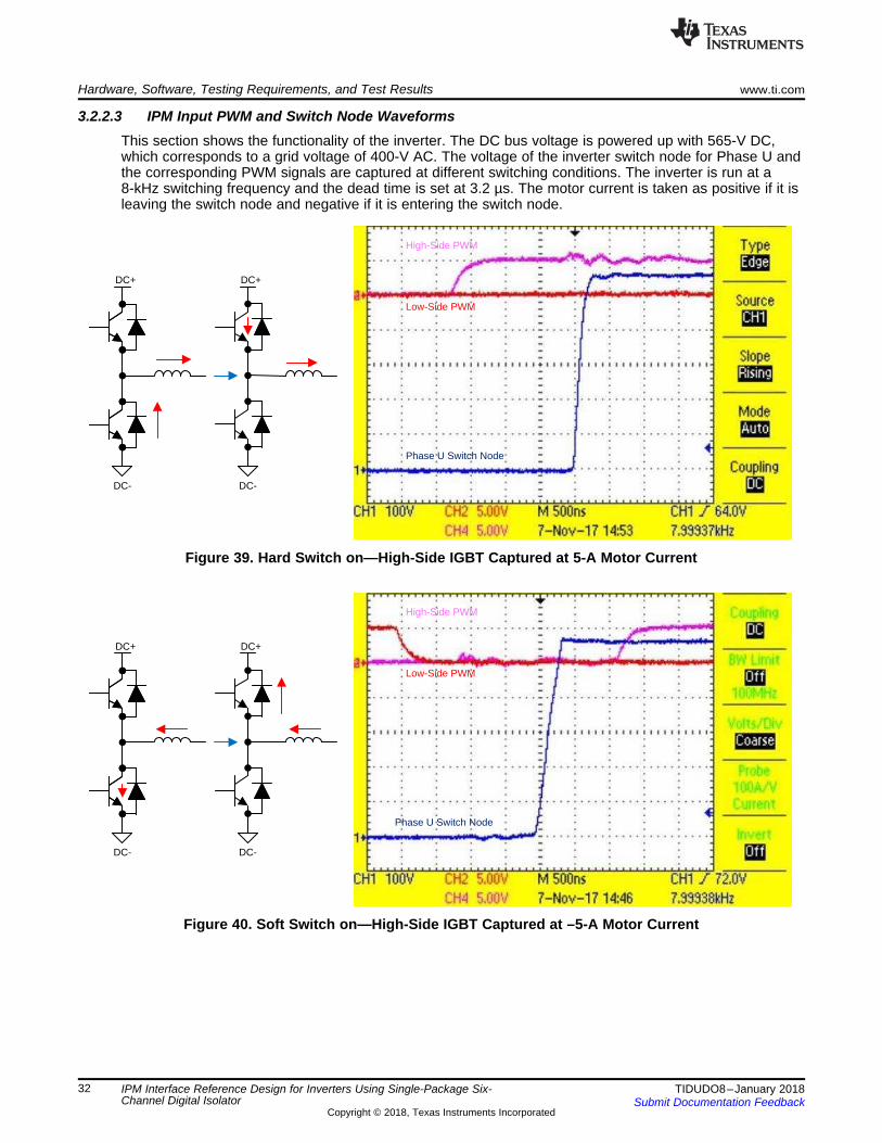
3.2.2.3 IPM Input PWM and Switch Node WaveformsThis section shows the functionality of the inverter. The DC bus voltage is powered up with 565-V DC,which corresponds to a grid voltage of 400-V AC. The voltage of the inverter switch node for Phase U andthe corresponding PWM signals are captured at different switching conditions. The inverter is run at a8-kHz switching frequency and the dead time is set at 3.2 µs. The motor current is taken as positive if it isleaving the switch node and negative if it is entering the switch node.
Figure 39. Hard Switch on—High-Side IGBT Captured at 5-A Motor Current
Figure 40. Soft Switch on—High-Side IGBT Captured at –5-A Motor Current

Low-Side PWM
Phase U Switch Node
High-Side PWM
DC- DC-
DC+DC+
Low-Side PWM
Phase U Switch Node
High-Side PWM
DC- DC-
DC+DC+
www.ti.com Hardware, Software, Testing Requirements, and Test Results
33TIDUDO8–January 2018Submit Documentation Feedback
Copyright © 2018, Texas Instruments Incorporated
IPM Interface Reference Design for Inverters Using Single-Package Six-Channel Digital Isolator
Figure 41. Hard Switch on—Low-Side IGBT Captured at –5-A Motor Current
Figure 42. Soft Switch on—Low-Side IGBT Captured at 5-A Motor Current

Low-Side Input PWM ± Phase U
High-Side Input PWM ± Phase U
Low-Side Output PWM ± Phase V
High-Side Output PWM ± Phase W
Low-Side Input PWM ± Phase U
High-Side Input PWM ± Phase U
Low-Side Output PWM ± Phase V
High-Side Output PWM ± Phase W
Low-Side Input PWM ± Phase U
High-Side Input PWM ± Phase U
Low-Side Output PWM ± Phase V
High-Side Output PWM ± Phase W
Low-Side Input PWM ± Phase U
High-Side Input PWM ± Phase U
Low-Side Output PWM ± Phase V
High-Side Output PWM ± Phase W
Low-Side Input PWM ± Phase U
High-Side Input PWM ± Phase U
Low-Side Output PWM ± Phase V
High-Side Output PWM ± Phase W
Low-Side Input PWM ± Phase U
High-Side Input PWM ± Phase U
Low-Side Output PWM ± Phase V
High-Side Output PWM ± Phase W
Hardware, Software, Testing Requirements, and Test Results www.ti.com
34 TIDUDO8–January 2018Submit Documentation Feedback
Copyright © 2018, Texas Instruments Incorporated
IPM Interface Reference Design for Inverters Using Single-Package Six-Channel Digital Isolator
3.2.2.4 PWM Interlocking Using Optional Add-on CardThis section shows the functionality of the add-on interlocking card. For testing the card, a PWM signal of8 kHz with a 3.2-µs dead time is used. The dead time is made purposefully negative to overlap the high-side and low-side PWM signals and show the interlocking function.
Figure 43. Normal Operation of High-Side and Low-SidePWM Signals (Phase U)
Figure 44. Negative Dead Time Fault PurposefullyIntroduced to Check Interlocking Function (Phase U)
Figure 45. Rising Edge of PWM Signal Interlock(Phase U)
Figure 46. Falling Edge of PWM Signal Interlock(Phase U)
Figure 47. Interlocking (Phase V) Figure 48. Interlocking (Phase W)

Earth reference Table referenceCapacitive clamp
Induction motorTIDA-01349 PCB Scope for monitoring motor current10-m power cable
EFT generator
www.ti.com Hardware, Software, Testing Requirements, and Test Results
35TIDUDO8–January 2018Submit Documentation Feedback
Copyright © 2018, Texas Instruments Incorporated
IPM Interface Reference Design for Inverters Using Single-Package Six-Channel Digital Isolator
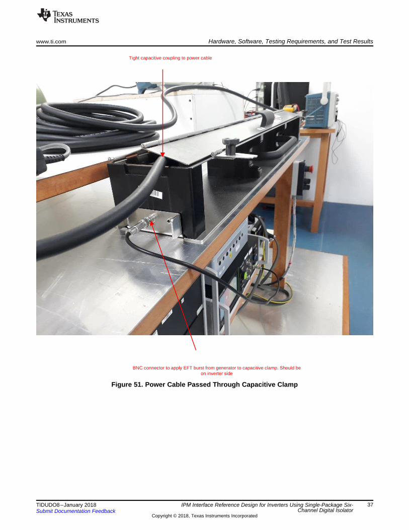
3.2.2.5 EFT on Motor Power InterfaceThis section shows the robustness of the ISO7760F to external EFT events. EFT pulses of differentamplitudes and polarities are applied on the power interface cable between the three-phase inverter andthe motor as shown in Figure 49. The tests are conducted according to IEC 61800-3, which refers to IEC61000-4-4 for EFT tests.
Figure 49 to Figure 52 show the setup for the EFT test. The power cable is passed through a 1-mcapacitive coupling clamp, through which EFT is injected into the cable. A 1-m cable length is maintainedfrom the capacitive clamp to the inverter. The inverter and the motor are placed on a wooden platform,which is at a height of 10 cm from the table reference. The cable shield is connected to the tablereference using a copper strap. This connection has the same effect as earthing the cable gland or collarin drive systems. The heat sink and the primary-side ground are also connected to the table reference.
Figure 49. EFT Test Setup

1-m length between inverter and capacitive
clamp
10-cm height platform
Hardware, Software, Testing Requirements, and Test Results www.ti.com
36 TIDUDO8–January 2018Submit Documentation Feedback
Copyright © 2018, Texas Instruments Incorporated
IPM Interface Reference Design for Inverters Using Single-Package Six-Channel Digital Isolator
Figure 50. Inverter and Motor Placed on Wooden Board at Height of 10 cm From Table Reference
Tight capacitive coupling to power cable
BNC connector to apply EFT burst from generator to capacitive clamp. Should be on inverter side
www.ti.com Hardware, Software, Testing Requirements, and Test Results
37TIDUDO8–January 2018Submit Documentation Feedback
Copyright © 2018, Texas Instruments Incorporated
IPM Interface Reference Design for Inverters Using Single-Package Six-Channel Digital Isolator
Figure 51. Power Cable Passed Through Capacitive Clamp

Copper strap connection from cable shield to table reference
Hardware, Software, Testing Requirements, and Test Results www.ti.com
38 TIDUDO8–January 2018Submit Documentation Feedback
Copyright © 2018, Texas Instruments Incorporated
IPM Interface Reference Design for Inverters Using Single-Package Six-Channel Digital Isolator
Figure 52. Connection of Shield of Power Cable to Table Reference

www.ti.com Hardware, Software, Testing Requirements, and Test Results
39TIDUDO8–January 2018Submit Documentation Feedback
Copyright © 2018, Texas Instruments Incorporated
IPM Interface Reference Design for Inverters Using Single-Package Six-Channel Digital Isolator
3.2.2.5.1 Test ConditionsThe 5-kHz EFT pulse bursts for 60 s. The burst duration is 15 ms and burst period is 300 ms. A typicalEFT pulse of 5 ns rise time, and a duration of 50 ns is used. For the test, a 10-m shielded 4 conductorcable is used (part number: V16016 BK005, manufacturer: Alpha wire). Three conductors are used for theUVW phases, and the fourth conductor is left floating. 565-V DC is applied to the inverter DC bus. Theinverter is switched at a frequency of 8 kHz, the motor frequency is set at 10 Hz, and the RMS voltageapplied to the motor is approximately 120 VRMS phase to phase.
3.2.2.5.2 Pass and Fail ConditionsThe motor must run continuously without any unusual sounds and without malfunction observed in thepower stage. Table 3 defines the performance criteria.
Table 3. EFT Test Performance Criteria
PERFORMANCE(ACCEPTANCE)
CRITERIONDESCRIPTION
A The module must continue to operate as intended. No loss of function or performance even during the test.
B Temporary degradation of performance during test is accepted. After the test, the module must continue tooperate as intended without manual intervention.
CDuring the test, loss of functions accepted, but no destruction of hardware or software. After the test, themodule must continue to operate as intended, after manual restart, power off, or power on. Not self-recoverable.
D Damage to hardware.
Table 4. EFT Results
EFT PULSES (kV) PERFORMANCE CRITERIA0.5 A
–0.5 A1 A
–1 A2 A
–2 A4 A
–4 A
NOTE: The EFT testing is done only for the PWM isolation subsystem while running the inverter inopen loop control. The current and voltage sensing are not characterized.

Data
IPM Control Power Supply
Fault
Data
IPM Control Power Supply
Fault
Data
IPM Control Power Supply
Fault
Data
IPM Control Power Supply
Fault
Hardware, Software, Testing Requirements, and Test Results www.ti.com
40 TIDUDO8–January 2018Submit Documentation Feedback
Copyright © 2018, Texas Instruments Incorporated
IPM Interface Reference Design for Inverters Using Single-Package Six-Channel Digital Isolator
3.2.2.6 Multiplexing Fault Signal With Temperature MeasurementIn this reference design, the IPM fault signal is multiplexed with the analog temperature signal to save anisolation channel. The IPM fault can be triggered by either an UVLO event on the IPM control powersupply or by a short-circuit detection in one of the low-side IGBT switches of the IPM. For the test, the IPMfault signal is activated by lowering the IPM control power supply from 15 V to 8 V. This new voltagetriggers the IPM UVLO diagnostic feature.
Figure 53 to Figure 55 show the fault signal multiplexing with the temperature measurement data. Thefault signal is an active low signal. As long as it is high, the delta-sigma modulator outputs the data to thecontroller. When the fault signal goes low, the input stage of the delta-sigma modulator is overranged. Thediagnostic feature of the delta-sigma modulator forces the output to zero with a bit toggle every 128 bits asshown in Figure 56.
Figure 53. Fault Signal Detection Figure 54. Fault Signal Detection Zoomed
Figure 55. Fault Detection Delay Across Isolator Figure 56. Bit Toggle Every 128 Bits

Reinforced isolation barrier 8-mm minimum creepage
www.ti.com Design Files
41TIDUDO8–January 2018Submit Documentation Feedback
Copyright © 2018, Texas Instruments Incorporated
IPM Interface Reference Design for Inverters Using Single-Package Six-Channel Digital Isolator
4 Design Files
4.1 SchematicsTo download the schematics, see the design files at TIDA-01349.
4.2 Bill of MaterialsTo download the bill of materials (BOM), see the design files at TIDA-01349.
4.3 PCB Layout Recommendations
4.3.1 Reinforced Isolation BarrierFigure 57 shows the isolation barrier and the ground split. The copper tracks on the high-voltage inverterside and the low-voltage controller side are separated from each other by a reinforced isolation barrier.The wide body package of the digital isolator and the delta-sigma modulators are placed across theisolation barrier. The creepage spacing of the isolation barrier is maintained to a minimum of 8 mm.
Figure 57. Reinforced Isolation Barrier and Creepage Spacing

Design Files www.ti.com
42 TIDUDO8–January 2018Submit Documentation Feedback
Copyright © 2018, Texas Instruments Incorporated
IPM Interface Reference Design for Inverters Using Single-Package Six-Channel Digital Isolator
4.3.2 Current SensingUse Kelvin connections on the shunt resistors for accurate current sensing as shown in Figure 58. Thecurrent sense signals are then routed like a differential pair to the delta-sigma modulator input stages. Thedifferential routing ensures that noise if any equally impacts both the current sense lines, and this will getrejected by the common-mode rejection of the delta-sigma modulator.
Figure 58. Kelvin Connection to Shunt Resistors
At the delta-sigma modulator, place the differential RC filter comprising of R2, R4, and C8 close to theinput stage of the device U3. Place the decoupling capacitor of the power supply (C5) close to the powersupply pins of the device and connect it directly without the use of vias. The TLV76050 LDO (U2), placedon the bottom side of the PCB (Figure 60), generates the 5-V supply for the delta-sigma modulator fromthe 15-V bootstrap supply and is placed close to the modulator. The small SOT-23 package of the LDOenables this while still managing to keep sufficient creepage distances from the neighboring high-voltagenets. Place input and output decoupling capacitors close to LDO.
Figure 59. AMC1303M0520 Layout Figure 60. LDO Placement

www.ti.com Design Files
43TIDUDO8–January 2018Submit Documentation Feedback
Copyright © 2018, Texas Instruments Incorporated
IPM Interface Reference Design for Inverters Using Single-Package Six-Channel Digital Isolator
4.3.3 LDO LayoutPlace input decoupling capacitors C50 and C53 close to input of LDO U10 and the output decouplingcapacitor C51 close to the output stage to improve PSRR, output noise, and transient response.
Figure 61. Layout for TPS70633
To improve AC performance like PSRR, output noise, and transient response of LDO U6, placedecoupling capacitors C47, C49, C19, and C18 close to the device. Place all the decoupling capacitors onthe same side of the PCB as the device. The metal pad beneath the device is connected to the DC-ground plane with multiple vias to further improve thermal performance of the package.
Figure 62. Layout for TPS7A4201

Design Files www.ti.com
44 TIDUDO8–January 2018Submit Documentation Feedback
Copyright © 2018, Texas Instruments Incorporated
IPM Interface Reference Design for Inverters Using Single-Package Six-Channel Digital Isolator
4.3.4 Layout PrintsTo download the layer plots, see the design files at TIDA-01349.
4.4 Altium ProjectTo download the Altium project files, see the design files at TIDA-01349.
4.5 Gerber FilesTo download the Gerber files, see the design files at TIDA-01349.
4.6 Assembly DrawingsTo download the assembly drawings, see the design files at TIDA-01349.
5 Related Documentation1. Texas Instruments, Sensored Field Oriented Control of 3-Phase Permanent Magnet Synchronous
Motors Using TMS320F2837x Application Report2. Texas Instruments, ISO72x Digital Isolator Magnetic-Field Immunity Application Report3. Mitsubishi Electric, 1200V LARGE DIPIPM Ver.6 Series APPLICATION NOTE PSS**SA2FT
5.1 TrademarksC2000, E2E, Delfino, controlSUITE, Code Composer Studio are trademarks of Texas Instruments.All other trademarks are the property of their respective owners.
6 TerminologyIGBT— Insulated gate bipolar transistor
IPM— Intelligent power modules
HVIC— High-voltage IC
LVIC— Low-voltage IC
PWM— Pulse width modulation
UVLO— Undervoltage lockout

IMPORTANT NOTICE FOR TI DESIGN INFORMATION AND RESOURCES
Texas Instruments Incorporated (‘TI”) technical, application or other design advice, services or information, including, but not limited to,reference designs and materials relating to evaluation modules, (collectively, “TI Resources”) are intended to assist designers who aredeveloping applications that incorporate TI products; by downloading, accessing or using any particular TI Resource in any way, you(individually or, if you are acting on behalf of a company, your company) agree to use it solely for this purpose and subject to the terms ofthis Notice.TI’s provision of TI Resources does not expand or otherwise alter TI’s applicable published warranties or warranty disclaimers for TIproducts, and no additional obligations or liabilities arise from TI providing such TI Resources. TI reserves the right to make corrections,enhancements, improvements and other changes to its TI Resources.You understand and agree that you remain responsible for using your independent analysis, evaluation and judgment in designing yourapplications and that you have full and exclusive responsibility to assure the safety of your applications and compliance of your applications(and of all TI products used in or for your applications) with all applicable regulations, laws and other applicable requirements. Yourepresent that, with respect to your applications, you have all the necessary expertise to create and implement safeguards that (1)anticipate dangerous consequences of failures, (2) monitor failures and their consequences, and (3) lessen the likelihood of failures thatmight cause harm and take appropriate actions. You agree that prior to using or distributing any applications that include TI products, youwill thoroughly test such applications and the functionality of such TI products as used in such applications. TI has not conducted anytesting other than that specifically described in the published documentation for a particular TI Resource.You are authorized to use, copy and modify any individual TI Resource only in connection with the development of applications that includethe TI product(s) identified in such TI Resource. NO OTHER LICENSE, EXPRESS OR IMPLIED, BY ESTOPPEL OR OTHERWISE TOANY OTHER TI INTELLECTUAL PROPERTY RIGHT, AND NO LICENSE TO ANY TECHNOLOGY OR INTELLECTUAL PROPERTYRIGHT OF TI OR ANY THIRD PARTY IS GRANTED HEREIN, including but not limited to any patent right, copyright, mask work right, orother intellectual property right relating to any combination, machine, or process in which TI products or services are used. Informationregarding or referencing third-party products or services does not constitute a license to use such products or services, or a warranty orendorsement thereof. Use of TI Resources may require a license from a third party under the patents or other intellectual property of thethird party, or a license from TI under the patents or other intellectual property of TI.TI RESOURCES ARE PROVIDED “AS IS” AND WITH ALL FAULTS. TI DISCLAIMS ALL OTHER WARRANTIES ORREPRESENTATIONS, EXPRESS OR IMPLIED, REGARDING TI RESOURCES OR USE THEREOF, INCLUDING BUT NOT LIMITED TOACCURACY OR COMPLETENESS, TITLE, ANY EPIDEMIC FAILURE WARRANTY AND ANY IMPLIED WARRANTIES OFMERCHANTABILITY, FITNESS FOR A PARTICULAR PURPOSE, AND NON-INFRINGEMENT OF ANY THIRD PARTY INTELLECTUALPROPERTY RIGHTS.TI SHALL NOT BE LIABLE FOR AND SHALL NOT DEFEND OR INDEMNIFY YOU AGAINST ANY CLAIM, INCLUDING BUT NOTLIMITED TO ANY INFRINGEMENT CLAIM THAT RELATES TO OR IS BASED ON ANY COMBINATION OF PRODUCTS EVEN IFDESCRIBED IN TI RESOURCES OR OTHERWISE. IN NO EVENT SHALL TI BE LIABLE FOR ANY ACTUAL, DIRECT, SPECIAL,COLLATERAL, INDIRECT, PUNITIVE, INCIDENTAL, CONSEQUENTIAL OR EXEMPLARY DAMAGES IN CONNECTION WITH ORARISING OUT OF TI RESOURCES OR USE THEREOF, AND REGARDLESS OF WHETHER TI HAS BEEN ADVISED OF THEPOSSIBILITY OF SUCH DAMAGES.You agree to fully indemnify TI and its representatives against any damages, costs, losses, and/or liabilities arising out of your non-compliance with the terms and provisions of this Notice.This Notice applies to TI Resources. Additional terms apply to the use and purchase of certain types of materials, TI products and services.These include; without limitation, TI’s standard terms for semiconductor products http://www.ti.com/sc/docs/stdterms.htm), evaluationmodules, and samples (http://www.ti.com/sc/docs/sampterms.htm).
Mailing Address: Texas Instruments, Post Office Box 655303, Dallas, Texas 75265Copyright © 2018, Texas Instruments Incorporated