ipc-a-610 f acceptability of electronic...
TRANSCRIPT
IPC-A-610 F
Acceptability of Electronic Assemblies
February 2011 Meeting Draft
Illustrations and text are copyright IPC and may be copied only for use in development of IPC-A-610 Revision E.
IPC-A-610 Revision F Draft February 2012
2 Illustrations and text are copyright IPC and may be copied only for use in development of IPC-A-610 Revision F

IPC-A-610 Revision F Draft February 2012
3 Illustrations and text are copyright IPC and may be copied only for use in development of IPC-A-610 Revision F
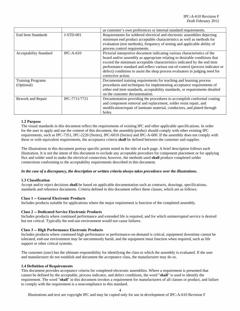
1 Forward The following topics are addressed in this section: <This Chapter ToC will be added at time of publication> If a conflict occurs between the English and translated versions of this document, the English version will take precedence. 1.1 Scope This standard is a collection of visual quality acceptability requirements for electronic assemblies. This document presents acceptance requirements for the manufacture of electrical and electronic assemblies. Historically, electronic assembly standards contained a more comprehensive tutorial addressing principles and techniques. For a more complete understanding of this document's recommendations and requirements, one may use this document in conjunction with IPC-HDBK-001, IPC-AJ-820 and IPC J-STD-001. The criteria in this standard are not intended to define processes to accomplish assembly operations nor is it intended to authorize repair/modification or change of the customer’s product. For instance, the presence of criteria for adhesive bonding of components does not imply/authorize/require the use of adhesive bonding, the depiction of a lead wrapped clockwise around a terminal does not imply/authorize/require that all leads/wires be wrapped in the clockwise direction. Users of this standard should be knowledgeable of the applicable requirements of the document and how to apply them. Objective evidence of the demonstration of this knowledge should be maintained. Where objective evidence is unavailable, the organization should consider periodic review of personnel skills to determine visual acceptance criteria appropriately. IPC-A-610 has criteria outside the scope of IPC J-STD-001 defining handling, mechanical and other workmanship requirements. Table 1-1 is a summary of related documents. IPC-AJ-820 is a supporting document that provides information regarding the intent of this specification content and explains or amplifies the technical rationale for transition of limits through Target to Defect condition criteria. In addition, supporting information is provided to give a broader understanding of the process considerations that are related to performance but not commonly distinguishable through visual assessment methods. The explanations provided in IPC-AJ-820 should be useful in determining disposition of conditions identified as Defect, processes associated with Process Indicators, as well as answering questions regarding clarification in use and application for defined content of this specification. Contractual reference to IPC-A-610 does not additionally impose the content of IPC-AJ-820 unless specifically referenced in contractual documentation. Table 1-1 Summary of Related Documents
Document Purpose Spec.# Definition Design Standard IPC-2220 (Series)
IPC-7351 IPC-CM-C770
Design requirements reflecting three levels of complexity (Levels A, B, and C) indicating finer geometries, greater densities, more process steps to produce the product. Component and Assembly Process Guidelines to assist in the design of the bare board and the assembly where the bare board processes concentrate on land patterns for surface mount and the assembly concentrates on surface mount and through-hole principles which are usually incorporated into the design process and the documentation.
PCB Requirements IPC-6010 (series) IPC-A-600
Requirements and acceptance documentation for rigid, rigid flex, flex and other types of substrates.
End Item Documentation IPC-D-325 Documentation depicting bare board specific end product requirements designed by the customer or end item assembly requirements. Details may or may not reference industry specifications or workmanship standards as well
IPC-A-610 Revision F Draft February 2012
4 Illustrations and text are copyright IPC and may be copied only for use in development of IPC-A-610 Revision F
as customer’s own preferences or internal standard requirements. End Item Standards J-STD-001 Requirements for soldered electrical and electronic assemblies depicting
minimum end product acceptable characteristics as well as methods for evaluation (test methods), frequency of testing and applicable ability of process control requirements.
Acceptability Standard IPC-A-610 Pictorial interpretive document indicating various characteristics of the board and/or assembly as appropriate relating to desirable conditions that exceed the minimum acceptable characteristics indicated by the end item performance standard and reflect various out-of-control (process indicator or defect) conditions to assist the shop process evaluators in judging need for corrective action.
Training Programs (Optional)
Documented training requirements for teaching and learning process procedures and techniques for implementing acceptance requirements of either end item standards, acceptability standards, or requirements detailed on the customer documentation.
Rework and Repair IPC-7711/7721 Documentation providing the procedures to accomplish conformal coating and component removal and replacement, solder resist repair, and modification/repair of laminate material, conductors, and plated through holes.
1.2 Purpose The visual standards in this document reflect the requirements of existing IPC and other applicable specifications. In order for the user to apply and use the content of this document, the assembly/product should comply with other existing IPC requirements, such as IPC-7351, IPC-2220 (Series), IPC-6010 (Series) and IPC-A-600. If the assembly does not comply with these or with equivalent requirements, the acceptance criteria shall be defined between the customer and supplier. The illustrations in this document portray specific points noted in the title of each page. A brief description follows each illustration. It is not the intent of this document to exclude any acceptable procedure for component placement or for applying flux and solder used to make the electrical connection; however, the methods used shall produce completed solder connections conforming to the acceptability requirements described in this document. In the case of a discrepancy, the description or written criteria always takes precedence over the illustrations. 1.3 Classification Accept and/or reject decisions shall be based on applicable documentation such as contracts, drawings, specifications, standards and reference documents. Criteria defined in this document reflect three classes, which are as follows: Class 1 -- General Electronic Products Includes products suitable for applications where the major requirement is function of the completed assembly. Class 2 -- Dedicated Service Electronic Products Includes products where continued performance and extended life is required, and for which uninterrupted service is desired but not critical. Typically the end-use environment would not cause failures. Class 3 -- High Performance Electronic Products Includes products where continued high performance or performance-on-demand is critical, equipment downtime cannot be tolerated, end-use environment may be uncommonly harsh, and the equipment must function when required, such as life support or other critical systems. The customer (user) has the ultimate responsibility for identifying the class to which the assembly is evaluated. If the user and manufacturer do not establish and document the acceptance class, the manufacturer may do so. 1.4 Definition of Requirements This document provides acceptance criteria for completed electronic assemblies. Where a requirement is presented that cannot be defined by the acceptable, process indicator, and defect conditions, the word "shall" is used to identify the requirement. The word "shall" in this document invokes a requirement for manufacturers of all classes or product, and failure to comply with the requirement is a noncompliance to this standard.
IPC-A-610 Revision F Draft February 2012
5 Illustrations and text are copyright IPC and may be copied only for use in development of IPC-A-610 Revision F
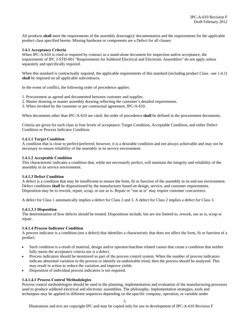
All products shall meet the requirements of the assembly drawing(s)/ documentation and the requirements for the applicable product class specified herein. Missing hardware or components are a Defect for all classes. 1.4.1 Acceptance Criteria When IPC-A-610 is cited or required by contract as a stand-alone document for inspection and/or acceptance, the requirements of IPC J-STD-001 "Requirements for Soldered Electrical and Electronic Assemblies" do not apply unless separately and specifically required. When this standard is contractually required, the applicable requirements of this standard (including product Class –see 1.4.1) shall be imposed on all applicable subcontracts. In the event of conflict, the following order of precedence applies: 1. Procurement as agreed and documented between customer and supplier. 2. Master drawing or master assembly drawing reflecting the customer’s detailed requirements. 3. When invoked by the customer or per contractual agreement, IPC-A-610. When documents other than IPC-A-610 are cited, the order of precedence shall be defined in the procurement documents. Criteria are given for each class in four levels of acceptance: Target Condition, Acceptable Condition, and either Defect Condition or Process Indicator Condition. 1.4.1.1 Target Condition A condition that is close to perfect/preferred, however, it is a desirable condition and not always achievable and may not be necessary to ensure reliability of the assembly in its service environment. 1.4.1.2 Acceptable Condition This characteristic indicates a condition that, while not necessarily perfect, will maintain the integrity and reliability of the assembly in its service environment. 1.4.1.3 Defect Condition A defect is a condition that may be insufficient to ensure the form, fit or function of the assembly in its end use environment. Defect conditions shall be dispositioned by the manufacturer based on design, service, and customer requirements. Disposition may be to rework, repair, scrap, or use as is. Repair or "use as is" may require customer concurrence. A defect for Class 1 automatically implies a defect for Class 2 and 3. A defect for Class 2 implies a defect for Class 3. 1.4.1.3.1 Disposition The determination of how defects should be treated. Dispositions include, but are not limited to, rework, use as is, scrap or repair. 1.4.1.4 Process Indicator Condition A process indicator is a condition (not a defect) that identifies a characteristic that does not affect the form, fit or function of a product. Such condition is a result of material, design and/or operator/machine related causes that create a condition that neither
fully meets the acceptance criteria nor is a defect. Process indicators should be monitored as part of the process control system. When the number of process indicators
indicate abnormal variation in the process or identify an undesirable trend, then the process should be analyzed. This may result in action to reduce the variation and improve yields.
Disposition of individual process indicators is not required. 1.4.1.4.1 Process Control Methodologies Process control methodologies should be used in the planning, implementation and evaluation of the manufacturing processes used to produce soldered electrical and electronic assemblies. The philosophy, implementation strategies, tools and techniques may be applied in different sequences depending on the specific company, operation, or variable under
IPC-A-610 Revision F Draft February 2012
6 Illustrations and text are copyright IPC and may be copied only for use in development of IPC-A-610 Revision F
consideration to relate process control and capability to end product requirements. The manufacturer needs to maintain objective evidence of a current process control/continuous improvement plan that is available for review. 1.4.1.5 Combined Conditions Cumulative conditions shall be considered in addition to the individual characteristics for product acceptability even though they are not individually considered defective. The significant number of combinations that could occur does not allow full definition in the content and scope of this specification but manufacturers should be vigilant for the possibility of combined and cumulative conditions and their impact upon product performance. Conditions of acceptability provided in this specification are individually defined and created with separate consideration for their impact upon reliable operation for the defined production classification. Where related conditions can be combined, the cumulative performance impact for the product may be significant; e.g., minimum solder fillet quantity when combined with maximum side overhang and minimum end overlap may cause a significant degradation of the mechanical attachment integrity. The manufacturer is responsible for identification of such conditions. The User is responsible to identify combined conditions where there is significant concern based upon end use environment and product performance requirements.<Sep2011> 1.4.1.6 Conditions Not Specified Conditions that are not specified as defective or as a process indicator may be considered acceptable unless it can be established that the condition affects user defined form, fit or function. 1.4.1.7 Specialized Designs IPC-A-610, as an industry consensus document, cannot address all of the possible components and product design combinations. Where uncommon or specialized technologies are used, it may be necessary to develop unique acceptance criteria. However, where similar characteristics exist, this document may provide guidance for product acceptance criteria. Often, unique definition is necessary to consider the specialized characteristics while considering product performance criteria. The development should include customer involvement or consent. For Class 3 the criteria shall include agreed definition of product acceptance. Whenever possible these criteria should be submitted to the IPC Technical Committee to be considered for inclusion in upcoming revisions of this standard. 1.5 Terms & Definitions Items noted with an * are quoted from IPC-T-50. 1.5.1 Board Orientation The following terms are used throughout this document to determine the board side. The source/destination side shall be considered when applying some criteria, such as that in Tables 7-4, 7-5 and 7-7. 1.5.1.1 *Primary Side That side of a packaging and interconnecting structure (PCB) that is so defined on the master drawing. (It is usually the side that contains the most complex or the most number of components. This side is sometimes referred to as the component side or solder destination side in through-hole mounting technology.) 1.5.1.2 *Secondary Side That side of a packaging and interconnecting structure (PCB) that is opposite the primary side. (This side is sometimes referred to as the solder side or solder source side in through-hole mounting technology.) 1.5.1.3 Solder Source Side The solder source side is that side of the PCB to which solder is applied. The solder source side is normally the secondary side of the PCB when wave, dip, or drag soldering are used. The solder source side may be the primary side of the PCB when hand soldering operations are conducted.

IPC-A-610 Revision F Draft February 2012
7 Illustrations and text are copyright IPC and may be copied only for use in development of IPC-A-610 Revision F
1.5.1.4 Solder Destination Side The solder destination side is that side of the PCB that the solder flows toward in a through-hole application. The destination is normally the primary side of the PCB when wave, dip or drag soldering is used. The destination side may be the secondary side of the PCB when hand-soldering operations are conducted. 1.5.2 *Cold Solder Connection A solder connection that exhibits poor wetting and that is characterized by a grayish porous appearance. (This is due to excessive impurities in the solder, inadequate cleaning prior to soldering, and/or the insufficient application of heat during the soldering process.) 1.5.3 Electrical Clearance Throughout this document the minimum spacing between non-common uninsulated conductors (e.g., patterns, materials, hardware, or residue) is referred to as “minimum electrical clearance.” It is defined in the applicable design standard or on the approved or controlled documentation. Insulating material needs to provide sufficient electrical isolation. In the absence of a known design standard use Appendix A (derived from IPC-2221). Any violation of minimum electrical clearance is a defect condition for all classes. 1.5.4 High Voltage The term “high voltage” will vary by design and application. The high voltage criteria in this document are only applicable when specifically required in the drawings/procurement documentation. 1.5.5 Intrusive Solder A process in which the solder paste for the through-hole components is applied using a stencil or syringe to accommodate through-hole components that are inserted and reflow-soldered together with the surface-mount components. 1.5.6 *Leaching The loss or removal of a basis metal or coating during a soldering operation.<Sep2011> 1.4.61.5.7 Meniscus (Component) Sealant or encapsulant on a lead, protruding from the seating plane of the component. This includes materials such as ceramic, epoxy or other composites, and flash from molded components. 1.5.71.5.8 *Nonfunctional Land A land that is not connected electrically to the conductive pattern on its layer. 1.5.81.5.9 Pin-in-Paste See Intrusive Solder 1.5.91.5.10 Wire Diameter In this document, wire diameter (D) is the overall diameter of conductor including insulation. Unless otherwise specified, criteria in this standard are applicable for solid wire/component leads or stranded wire. 1.5.101.5.11 Wire Overwrap A wire/lead that is wrapped more than 360° and remains in contact with the terminal post, Figure 6-64A. 1.5.111.5.12 Wire Overlap A wire/lead that is wrapped more than 360° and crosses over itself, i.e., does not remain in contact with the terminal post, Figure 6-64B. 1.6 Examples and Illustrations Many of the examples (illustrations) shown are grossly exaggerated in order to depict the reasons for this classification. It is necessary that users of this standard pay particular attention to the subject of each section to avoid misinterpretation. 1.7 Inspection Methodology Accept and/or reject decisions shall be based on applicable documentation such as contract, drawings, specifications and referenced documents.

IPC-A-610 Revision F Draft February 2012
8 Illustrations and text are copyright IPC and may be copied only for use in development of IPC-A-610 Revision F
The inspector does not select the class for the assembly under inspection, see 1.3. Documentation that specifies the applicable class for the assembly under inspection shall be provided to the inspector. Automated Inspection Technology (AIT) is a viable alternative to visual inspection and complements automated test equipment. Many of the characteristics in this document can be inspected with an AIT system. IPC-AI-641 "User's Guidelines for Automated Solder Joint Inspection Systems" and IPC-AI-642 "User's Guidelines for Automated Inspection of Artwork, Inner-layers, and Unpopulated PCBs" provide more information on automated inspection technologies. If the customer desires the use of industry standard requirements for frequency of inspection and acceptance, J-STD-001 is recommended for further soldering requirement details. 1.8 Verification of Dimensions The actual measurements provided in this document (i.e., specific part mounting and solder fillet dimensions and determination of percentages) are not required except for referee purposes. All dimensions in this standard are expressed in SI (System International) units (with Imperial English equivalent dimensions provided in brackets). All specified limits in this standard are absolute limits as defined in ASTM E29. 1.9 Magnification Aids For visual inspection, some individual specifications may call for magnification aids for examining printed board assemblies. The tolerance for magnification aids is 15% of the selected magnification power. Magnification aids, if used for inspection, shall be appropriate with the item being inspected. Unless magnification requirements are otherwise specified by contractual documentation, the magnifications in Table 1-2 and Table 1-3 are determined by the item being inspected. Referee conditions are used to verify product rejected at the inspection magnification power. For assemblies with mixed land widths, the greater magnification may be used for the entire assembly. Table 1-2 Inspection Magnification (Land Width)
Land Widths or Land Diameters1 Magnification Power
Inspection Range Maximum Referee
> 1.0 mm [0.0394 in] 1.5X to 3X 4X
>0.5 to ≤1.0 mm [0.0197 to 0.0394 in] 3X to 7.5X 10X
≥0.25 to ≤0.5 mm [0.00984 to 0.0197 in] 7.5X to 10X 20X
< 0.25 mm 0.00984 in] 20X 40X
Note 1: A portion of a conductive pattern used for the connection and/or attachment of components. Table 1-3 Magnification Aid Applications – Other
Cleanliness (with or without cleaning processes) Magnification not required, see Note 1
Cleanliness (no-clean processes) Note 1
Conformal Coating/Encapsulation Notes 1,2
Marking Note 2
Other (Component and wire damage, etc.) Note 1
Note 1: Visual inspection may require the use of magnification, e.g. when fine pitch or high density assemblies are present, magnification may be needed to determine if contamination affects form, fit or function. Note 2: If magnification is used it is limited to 4X maximum. 1.10 Lighting Lighting shall be adequate for the item being inspected. Illumination at the surface of workstations should be at least 1000 lm/m2 [approximately 93 foot candles]. Light sources should be selected to prevent shadows.
IPC-A-610 Revision F Draft February 2012
9 Illustrations and text are copyright IPC and may be copied only for use in development of IPC-A-610 Revision F
Note: In selecting a light source, the color temperature of the light is an important consideration. Light ranges from 3000-5000° K enable users to distinguish various printed circuit assembly features and contaminates with increased clarity.
IPC-A-610 Revision F Draft February 2012
10 Illustrations and text are copyright IPC and may be copied only for use in development of IPC-A-610 Revision F
Section 2 Applicable Documents will be added at time of publication.
IPC-A-610 Revision F Draft February 2012
3- 1 Illustrations and text are copyright IPC and may be copied only for use in licensed translation of IPC-A-610 Revision F.
3 Handling Electronic Assemblies Protecting the Assembly – EOS/ESD and Other Handling Considerations The following topics are addressed in this section: <This Chapter ToC will be added at time of publication> 3.1 EOS/ESD Prevention Electrostatic Discharge (ESD) is the rapid transfer of a static electric charge from one object to another of a different potential that was created from electrostatic sources. When an electrostatic charge is allowed to come in contact with or close to a sensitive component it can cause damage to the component. Electrical Overstress (EOS) is the internal result of an unwanted application of electrical energy that results in damaged components. This damage can be from many different sources, such as electrically powered process equipment or ESD occurring during handling or processing. Electrostatic Discharge Sensitive (ESDS) components are those components that are affected by these high-electrical energy surges. The relative sensitivity of a component to ESD is dependent upon its construction and materials. As components become smaller and operate faster, the sensitivity increases. ESDS components can fail to operate or change in value as a result of improper handling or processing. These failures can be immediate or latent. The result of immediate failure can be additional testing and rework or scrap. However the consequences of latent failure are the most serious. Even though the product may have passed inspection and functional test, it may fail after it has been delivered to the customer. It is important to build protection for ESDS components into circuit designs and packaging. In the manufacturing and assembly areas, work is often done with unprotected electronic assemblies (such as test fixtures) that are attached to the ESDS components. It is important that ESDS items be removed from their protective enclosures only at EOS/ESD safe workstations within Electrostatic Protected Areas (EPA). This section is dedicated to safe handling of these unprotected electronic assemblies. Information in this section is intended to be general in nature. Additional information can be found in IPC J-STD-001, ANSI/ESD-S-20.20 and other related documents.
IPC-A-610 Revision F Draft February 2012
3- 2 Illustrations and text are copyright IPC and may be copied only for use in licensed translation of IPC-A-610 Revision F.
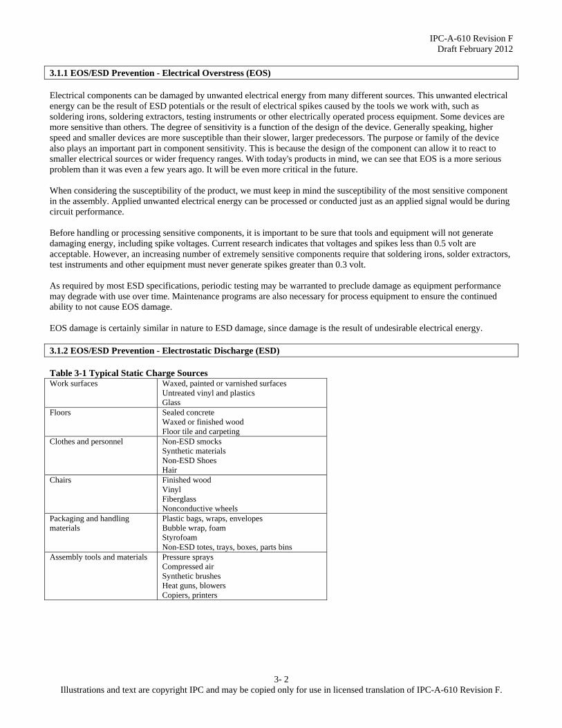
3.1.1 EOS/ESD Prevention - Electrical Overstress (EOS) Electrical components can be damaged by unwanted electrical energy from many different sources. This unwanted electrical energy can be the result of ESD potentials or the result of electrical spikes caused by the tools we work with, such as soldering irons, soldering extractors, testing instruments or other electrically operated process equipment. Some devices are more sensitive than others. The degree of sensitivity is a function of the design of the device. Generally speaking, higher speed and smaller devices are more susceptible than their slower, larger predecessors. The purpose or family of the device also plays an important part in component sensitivity. This is because the design of the component can allow it to react to smaller electrical sources or wider frequency ranges. With today's products in mind, we can see that EOS is a more serious problem than it was even a few years ago. It will be even more critical in the future. When considering the susceptibility of the product, we must keep in mind the susceptibility of the most sensitive component in the assembly. Applied unwanted electrical energy can be processed or conducted just as an applied signal would be during circuit performance. Before handling or processing sensitive components, it is important to be sure that tools and equipment will not generate damaging energy, including spike voltages. Current research indicates that voltages and spikes less than 0.5 volt are acceptable. However, an increasing number of extremely sensitive components require that soldering irons, solder extractors, test instruments and other equipment must never generate spikes greater than 0.3 volt. As required by most ESD specifications, periodic testing may be warranted to preclude damage as equipment performance may degrade with use over time. Maintenance programs are also necessary for process equipment to ensure the continued ability to not cause EOS damage. EOS damage is certainly similar in nature to ESD damage, since damage is the result of undesirable electrical energy. 3.1.2 EOS/ESD Prevention - Electrostatic Discharge (ESD) Table 3-1 Typical Static Charge Sources Work surfaces Waxed, painted or varnished surfaces
Untreated vinyl and plastics Glass
Floors Sealed concrete Waxed or finished wood Floor tile and carpeting
Clothes and personnel Non-ESD smocks Synthetic materials Non-ESD Shoes Hair
Chairs Finished wood Vinyl Fiberglass Nonconductive wheels
Packaging and handling materials
Plastic bags, wraps, envelopes Bubble wrap, foam Styrofoam Non-ESD totes, trays, boxes, parts bins
Assembly tools and materials Pressure sprays Compressed air Synthetic brushes Heat guns, blowers Copiers, printers

IPC-A-610 Revision F Draft February 2012
3- 3 Illustrations and text are copyright IPC and may be copied only for use in licensed translation of IPC-A-610 Revision F.
Table 3-2 Typical Static Voltage Generation Source 10-20% humidity 65-90% humidity
Walking on carpet 35,000 volts 1,500 volts Walking on vinyl flooring 12,000 volts 250 volts Worker at a bench 6,000 volts 100 volts Vinyl envelopes (Work Instructions) 7,000 volts 600 volts Plastic bag picked up from the bench 20,000 volts 1,200 volts Work chair with foam pad 18,000 volts 1,500 volts The best ESD damage prevention is a combination of preventing static charges and eliminating static charges if they do occur. All ESD protection techniques and products address one or both of the two issues. ESD damage is the result of electrical energy that was generated from static sources either being applied or in close proximity to ESDS devices. Static sources are all around us. The degree of static generated is relative to the characteristics of the source. To generate energy, relative motion is required. This could be contacting, separation, or rubbing of the material. Most of the serious offenders are insulators since they concentrate energy where it was generated or applied rather than allowing it to spread across the surface of the material. See Table 3-1. Common materials such as plastic bags or Styrofoam containers are serious static generators and are not appropriate in processing areas especially static safe/Electrostatic Protected Areas (EPA). Peeling adhesive tape from a roll can generate 20,000 volts. Even compressed air nozzles that move air over insulating surfaces generate charges. Destructive static charges are often induced on nearby conductors, such as human skin, and discharged into conductors on the assembly. This can happen when a person having an electrostatic charge potential touches a printed board assembly. The electronic assembly can be damaged as the discharge passes through the conductive pattern to an ESDS component. Electrostatic discharges may be too low to be felt by humans (less than static 3500 volts), and still damage ESDS components. Typical static voltage generation is included in Table 3-2. 3.1.3 EOS/ESD Prevention - Warning Labels Warning labels are available for posting in facilities and placement on devices, assemblies, equipment and packages to alert people to the possibility of inflicting electrostatic or electrical overstress damage to the devices they are handling. Examples of frequently encountered labels are shown in Figure 3-1. Symbol (1) ESD susceptibility symbol is a triangle with a reaching hand and a slash across it. This is used to indicate that an electrical or electronic device or assembly is susceptible to damage from an ESD event. Figure 3-1 610E Fig 3-1 1. ESD Susceptibility Symbol 2. ESD Protective Symbol Symbol (2) ESD protective symbol differs from the ESD susceptibility symbol in that it has an arc around the outside of the triangle and no slash across the hand. This is used to identify items that are specifically designed to provide ESD protection for ESD sensitive assemblies and devices. Symbols (1) and (2) identify devices or an assembly as containing devices that are ESD sensitive, and that they must be handled accordingly. These symbols are promoted by the ESD association and are described in EOS/ESD standard S8.1 as well as the Electronic Industries Association (EIA) in EIA-471, IEC/TS 61340-5-1, and other standards. Note that the absence of a symbol does not necessarily mean that the assembly is not ESD sensitive. When doubt exists about the sensitivity of an assembly, it must be handled as a sensitive device until it is determined otherwise.

IPC-A-610 Revision F Draft February 2012
3- 4 Illustrations and text are copyright IPC and may be copied only for use in licensed translation of IPC-A-610 Revision F.
3.1.4 EOS/ESD Prevention - Protective Materials ESDS components and assemblies must be protected from static sources when not being worked on in static safe environments or workstations. This protection could be conductive static-shielding boxes, protective caps, bags or wraps. ESDS items must be removed from their protective enclosures only at static safe workstations. It is important to understand the difference between the three types of protective enclosure material: (1) static shielding (or barrier packaging), (2) antistatic, and (3) static dissipative materials. Static shielding packaging will prevent an electrostatic discharge from passing through the package and into the assembly causing damage. Antistatic (low charging) packaging materials are used to provide inexpensive cushioning and intermediate packaging for ESDS items. Antistatic materials do not generate charges when motion is applied. However, if an electrostatic discharge occurs, it could pass through the packaging and into the part or assembly, causing EOS/ESD damage to ESDS components. Static dissipative materials have enough conductivity to allow applied charges to dissipate over the surface relieving hot spots of energy. Parts leaving an EOS/ESD protected work area must be overpacked in static shielding materials, which normally also have static dissipative and antistatic materials inside. Do not be misled by the "color" of packaging materials. It is widely assumed that "black" packaging is static shielding or conductive and that "pink" packaging is antistatic in nature. While that may be generally true, it can be misleading. In addition, there are many clear materials now on the market that may be antistatic and even static shielding. At one time, it could be assumed that clear packing materials introduced into the manufacturing operation would represent an EOS/ESD hazard. This is not necessarily the case now. Caution: Some static shielding and antistatic materials and some topical antistatic solutions may affect the solderability of assemblies, components, and materials in process. Care should be taken to select only packaging and handling materials that will not contaminate the assembly and use them with regard for the vendor’s instructions. Solvent cleaning of static dissipative or antistatic surfaces can degrade their ESD performance. Follow the manufacturer's recommendations for cleaning. 3.2 EOS/ESD Safe Workstation/EPA An EOS/ESD safe workstation prevents damage to sensitive components from spikes and static discharges while operations are being performed. Safe workstations should include EOS damage prevention by avoiding spike generating repair, manufacturing or testing equipment. Soldering irons, solder extractors and testing instruments can generate energy of sufficient levels to destroy extremely sensitive components and seriously degrade others. For ESD protection, a path-to-ground must be provided to neutralize static charges that might otherwise discharge to a device or assembly. ESD safe workstations/EPAs also have static dissipative or antistatic work surfaces that are connected to a common ground. Provisions are also made for grounding the worker's skin, preferably via a wrist strap to eliminate charges generated on the skin or clothing. Provision must be made in the grounding system to protect the worker from live circuitry as the result of carelessness or equipment failure. This is commonly accomplished through resistance in line with the ground path, which also slows the charge decay time to prevent sparks or surges of energy from ESD sources. Additionally, a survey must be performed of the available voltage sources that could be encountered at the workstation to provide adequate protection from personnel electrical hazards. For maximum allowable resistance and discharge times for static safe operations, see Table 3-3.

IPC-A-610 Revision F Draft February 2012
3- 5 Illustrations and text are copyright IPC and may be copied only for use in licensed translation of IPC-A-610 Revision F.
Table 3-3 Maximum Allowable Resistance and Discharge Times for Static Safe Operations Reading from Operator Through Maximum Tolerable Resistance Maximum Acceptable Discharge Time
Floor mat to ground 1000 megohms less than 1 sec. Table mat to ground 1000 megohms less than 1 sec. Wrist strap to ground 100 megohms less than 0.1 sec.
Note: The selection of resistance values is based on the available voltages at the station to ensure personnel safety as well as to provide adequate decay or discharge time for ESD potentials. Examples of acceptable workstations are shown in Figures 3-2 and 3-3. When necessary, air ionizers may be required for more sensitive applications. The selection, location, and use procedures for ionizers must be followed to ensure their effectiveness Figure 3-2 Series Connected Wrist Strap 610E Fig 3-2 1. Personal wrist strap 2. EOS protective trays, shunts, etc. 3. EOS protective table top 4. EOS protective floor or mat 5. Building floor 6. Common ground point 7. Ground Figure 3-3 Parallel Connected Wrist Strap 610E Fig 3-3 1. Personal wrist strap 2. EOS protective trays, shunts, etc. 3. EOS protective table top 4. EOS protective floor or mat 5. Building floor 6. Common ground point 7. Ground Keep workstation(s) free of static generating materials such as Styrofoam, plastic solder removers, sheet protectors, plastic or paper notebook folders, and employees' personal items. Periodically check workstations/EPAs to make sure they work. EOS/ESD assembly and personnel hazards can be caused by improper grounding methods or by an oxide build-up on grounding connectors. Tools and equipment must be periodically checked and maintained to ensure proper operation. Note: Because of the unique conditions of each facility, particular care must be given to "third wire" ground terminations. Frequently, instead of being at workbench or earth potential, the third wire ground may have a "floating" potential of 80 to 100 volts. This 80 to 100 volt potential between an electronic assembly on a properly grounded EOS/ESD workstation/EPA and a third wire grounded electrical tool may damage EOS sensitive components or could cause injury to personnel. Most ESD specifications also require these potentials to be electrically common. The use of ground fault interrupter (GFI) electrical outlets at EOS/ESD workstations/EPAs is highly recommended.
IPC-A-610 Revision F Draft February 2012
3- 6 Illustrations and text are copyright IPC and may be copied only for use in licensed translation of IPC-A-610 Revision F.
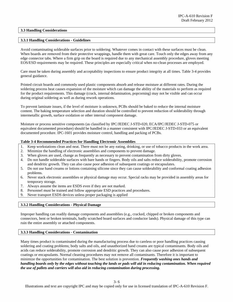
3.3 Handling Considerations 3.3.1 Handling Considerations - Guidelines Avoid contaminating solderable surfaces prior to soldering. Whatever comes in contact with these surfaces must be clean. When boards are removed from their protective wrappings, handle them with great care. Touch only the edges away from any edge connector tabs. Where a firm grip on the board is required due to any mechanical assembly procedure, gloves meeting EOS/ESD requirements may be required. These principles are especially critical when no-clean processes are employed. Care must be taken during assembly and acceptability inspections to ensure product integrity at all times. Table 3-4 provides general guidance. Printed circuit boards and commonly used plastic components absorb and release moisture at different rates. During the soldering process heat causes expansion of the moisture which can damage the ability of the materials to perform as required for the product requirements. This damage (crack, internal delamination, popcorning) may not be visible and can occur during original soldering as well as during rework operations. To prevent laminate issues, if the level of moisture is unknown, PCBs should be baked to reduce the internal moisture content. The baking temperature selection and duration should be controlled to prevent reduction of solderability through intermetallic growth, surface oxidation or other internal component damage. Moisture or process sensitive components (as classified by IPC/JEDEC J-STD-020, ECA/IPC/JEDEC J-STD-075 or equivalent documented procedure) should be handled in a manner consistent with IPC/JEDEC J-STD-033 or an equivalent documented procedure. IPC-1601 provides moisture control, handling and packing of PCBs. Table 3-4 Recommended Practices for Handling Electronic Assemblies 1. Keep workstations clean and neat. There must not be any eating, drinking, or use of tobacco products in the work area. 2. Minimize the handling of electronic assemblies and components to prevent damage. 3. When gloves are used, change as frequently as necessary to prevent contamination from dirty gloves. 4. Do not handle solderable surfaces with bare hands or fingers. Body oils and salts reduce solderability, promote corrosion
and dendritic growth. They can also cause poor adhesion of subsequent coatings or encapsulates. 5. Do not use hand creams or lotions containing silicone since they can cause solderability and conformal coating adhesion
problems. 6. Never stack electronic assemblies or physical damage may occur. Special racks may be provided in assembly areas for
temporary storage. 7. Always assume the items are ESDS even if they are not marked. 8. Personnel must be trained and follow appropriate ESD practices and procedures. 9. Never transport ESDS devices unless proper packaging is applied 3.3.2 Handling Considerations - Physical Damage Improper handling can readily damage components and assemblies (e.g., cracked, chipped or broken components and connectors, bent or broken terminals, badly scratched board surfaces and conductor lands). Physical damage of this type can ruin the entire assembly or attached components. 3.3.3 Handling Considerations - Contamination Many times product is contaminated during the manufacturing process due to careless or poor handling practices causing soldering and coating problems; body salts and oils, and unauthorized hand creams are typical contaminants. Body oils and acids can reduce solderability, promote corrosion and dendritic growth. They can also cause poor adhesion of subsequent coatings or encapsulants. Normal cleaning procedures may not remove all contaminants. Therefore it is important to minimize the opportunities for contamination. The best solution is prevention. Frequently washing ones hands and handling boards only by the edges without touching the lands or pads will aid in reducing contamination. When required the use of pallets and carriers will also aid in reducing contamination during processing.

IPC-A-610 Revision F Draft February 2012
3- 7 Illustrations and text are copyright IPC and may be copied only for use in licensed translation of IPC-A-610 Revision F.
The use of gloves or finger cots many times creates a false sense of protection and within a short time can become more contaminated than bare hands. When gloves or finger cots are used they should be discarded and replaced often. Gloves and finger cots need to be carefully chosen and properly utilized. 3.3.4 Handling Considerations - Electronic Assemblies Even if no ESDS markings are on an assembly, it still needs to be handled as if it were an ESDS assembly. However, ESDS components and electronic assemblies need to be identified by suitable EOS/ESD labels (see Figure 3-1). Many sensitive assemblies will also be marked on the assembly itself, usually on an edge connector. To prevent ESD and EOS damage to sensitive components, all handling, unpacking, assembly and testing shall be performed at a static controlled workstation (see Figures 3-2 and 3-3). 3.3.5 Handling Considerations - After Soldering After soldering and cleaning operations, the handling of electronic assemblies still requires great care. Fingerprints are extremely hard to remove and will often show up in conformally coated boards after humidity or environmental testing. Gloves or other protective handling devices may be used to prevent such contamination. Use mechanical racking or baskets with full ESD protection when handling during cleaning operations. 3.3.6 Handling Considerations - Gloves and Finger Cots The use of gloves or finger cots may be required under contract to prevent contamination of parts and assemblies. Gloves and finger cots must be carefully chosen to maintain EOS/ESD protection.
Figures 3-4 and 3-5 provide examples of: Handling with clean gloves and full EOS/ESD
protection. Handling during cleaning procedures using
solvent resistant gloves meeting all EOS/ESD requirements.
Handling with clean hands by board edges using full EOS/ESD protection.
Note: Any assembly related component if handled without EOS/ESD protection may damage electrostatic sensitive components. This damage could be in the form of latent failures, or product degradation not detectable during initial test or catastrophic failures found at initial test.
Figure 3-4 610E Fig 3-4
Figure 3-5 610E Fig 3-5
IPC-A-610 Revision F Draft February 2012
4- 1 Illustrations and text are copyright IPC and may be copied only for use in development of IPC-A-610 Revision F
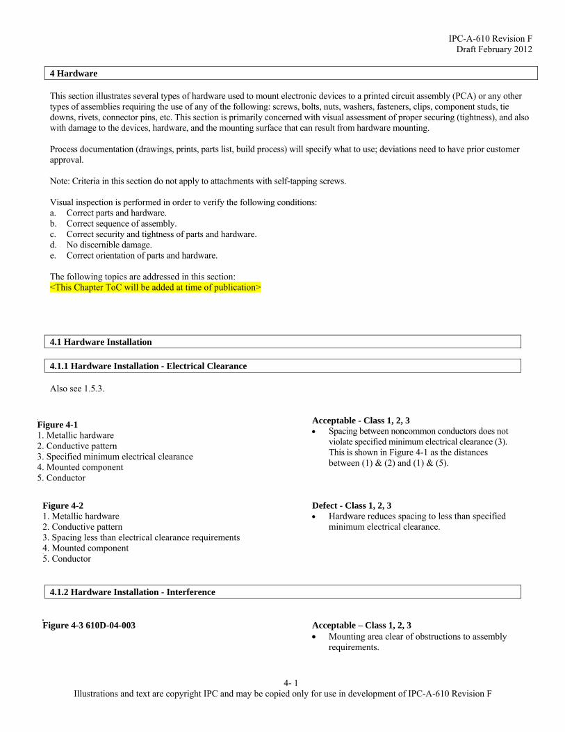
4 Hardware This section illustrates several types of hardware used to mount electronic devices to a printed circuit assembly (PCA) or any other types of assemblies requiring the use of any of the following: screws, bolts, nuts, washers, fasteners, clips, component studs, tie downs, rivets, connector pins, etc. This section is primarily concerned with visual assessment of proper securing (tightness), and also with damage to the devices, hardware, and the mounting surface that can result from hardware mounting. Process documentation (drawings, prints, parts list, build process) will specify what to use; deviations need to have prior customer approval. Note: Criteria in this section do not apply to attachments with self-tapping screws. Visual inspection is performed in order to verify the following conditions: a. Correct parts and hardware. b. Correct sequence of assembly. c. Correct security and tightness of parts and hardware. d. No discernible damage. e. Correct orientation of parts and hardware. The following topics are addressed in this section: <This Chapter ToC will be added at time of publication> 4.1 Hardware Installation 4.1.1 Hardware Installation - Electrical Clearance Also see 1.5.3.
Acceptable - Class 1, 2, 3 Spacing between noncommon conductors does not
violate specified minimum electrical clearance (3). This is shown in Figure 4-1 as the distances between (1) & (2) and (1) & (5).
Defect - Class 1, 2, 3 Hardware reduces spacing to less than specified
minimum electrical clearance.
4.1.2 Hardware Installation - Interference
Acceptable – Class 1, 2, 3 Mounting area clear of obstructions to assembly
requirements.
Figure 4-1 1. Metallic hardware 2. Conductive pattern 3. Specified minimum electrical clearance 4. Mounted component 5. Conductor
Figure 4-2 1. Metallic hardware 2. Conductive pattern 3. Spacing less than electrical clearance requirements 4. Mounted component 5. Conductor
Figure 4-3 610D-04-003

IPC-A-610 Revision F Draft February 2012
4- 2 Illustrations and text are copyright IPC and may be copied only for use in development of IPC-A-
610 Revision F
Defect - Class 1, 2, 3 Excess solder (uneven) on mounting holes where
mechanical assembly will be affected. Anything that interferes with mounting of
required hardware.
4.1.3 Heatsinks 4.1.3.1 Heatsinks - Insulators and Thermal Compounds This section illustrates various types of heatsink mounting. Bonding with thermally conductive adhesives may be specified in place of hardware. Visual inspection includes hardware security, component damage, and correct sequence of assembly. The following additional issues shall be considered: The component has good contact with the heatsink. The hardware secures the component to the heatsink. The component and heatsink are flat and parallel to each other. The thermal compound/insulator (mica, silicone grease, plastic film, etc.) is applied properly. \
Target - Class 1, 2, 3 Uniform border of mica, plastic film or thermal
compound showing around edges of component. Acceptable - Class 1, 2, 3 Not uniform but evidence of mica, plastic film or
thermal compound showing around edges of component.
Defect - Class 1, 2, 3 No evidence of insulating materials, or thermal
compound (if required). Thermal compound precludes formation of
required solder connection.
4.1.3.2 Heatsink - Contact
Target - Class 1, 2, 3 Component and heatsink are in full contact with
the mounting surface. Hardware meets specified attachment
requirements.
Figure 4-4
Figure 4-5
Figure 4-6
Figure 4-7 1. Heat sink
IPC-A-610 Revision F Draft February 2012
4- 3 Illustrations and text are copyright IPC and may be copied only for use in development of IPC-A-
610 Revision F
Acceptable - Class 1, 2, 3 Component not flush. Minimum 75% contact with mounting surface. Hardware meets mounting torque requirements if
specified. Defect - Class 1, 2, 3 Component has less than 75% contact with
mounting surface. Hardware is loose.
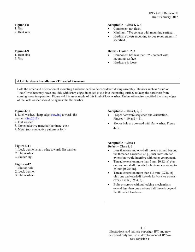
4.1.4 Hardware Installation - Threaded Fasteners Both the order and orientation of mounting hardware need to be considered during assembly. Devices such as “star” or “tooth” washers may have one side with sharp edges intended to cut into the mating surface to keep the hardware from coming loose in operation. Figure 4-11 is an example of this kind of lock washer. Unless otherwise specified the sharp edges of the lock washer should be against the flat washer.
Acceptable - Class 1, 2, 3 Proper hardware sequence and orientation.
Figures 4-10 and 4-11.
Slot or hole are covered with flat washer, Figure
4-12. Acceptable - Class 1 Defect – Class 2, 3 Less than one and one-half threads extend beyond
the threaded hardware, (e.g., nut) unless thread extension would interfere with other component.
Thread extension more than 3 mm [0.12 in] plus one and one-half threads for bolts or screws up to 25 mm [0.984 in].
Thread extension more than 6.3 mm [0.248 in] plus one and one-half threads for bolts or screws over 25 mm [0.984 in].
Bolts or screws without locking mechanisms extend less than one and one half threads beyond the threaded hardware.
Figure 4-8 1. Gap 2. Heat sink
Figure 4-9 1. Heat sink 2. Gap
Figure 4-10 1. Lock washer, sharp edge showing towards flat washer <Sep2011> 2. Flat washer 3. Nonconductive material (laminate, etc.) 4. Metal (not conductive pattern or foil)
Figure 4-11 1. Lock washer, sharp edge towards flat washer 2. Flat washer 3. Solder lug Figure 4-12 1. Slot or hole 2. Lock washer 3. Flat washer

IPC-A-610 Revision F Draft February 2012
4- 4 Illustrations and text are copyright IPC and may be copied only for use in development of IPC-A-
610 Revision F
Defect - Class 1, 2, 3 Thread extension interferes with adjacent
component. Hardware material or sequence not in
conformance with drawing. Lock washer against nonmetal/laminate. Flat washer missing, Figures 4-13, 4-15. Hardware missing or improperly installed, Figure
4-14.
4.1.4.1 Hardware Installation - Threaded Fasteners –Torque Where torque requirements are not specified, follow standard industry practices. \
Acceptable - Class 1, 2, 3 Fasteners are tight and split-ring lock washers,
when used, are fully compressed. Fastener torque value, if specified, is within
limits. Defect - Class 1, 2, 3 Lock washer not compressed. Fastener torque value, if specified, is not within
limits.
4.1.4.2 Hardware Installation – Threaded Fasteners - Wires When the use of terminal lugs is not required, wires are wrapped around screw type terminals in a manner that precludes loosening when the screw is tightened, and the ends of the wire are kept short to preclude shorting to ground or other current carrying conductors. If a washer is used, the wire/lead is mounted under the washer. Unless otherwise noted, all requirements apply to both stranded and solid wires. Special hardware staking/securing criteria may be required.
Target – Class 1, 2, 3 Original lay of the strands is not disturbed
(stranded wire). Wire wrapped a minimum of 270 around the
screw body. Wire end secured under screw head. Wire wrapped in the correct direction. All strands are under screw head.
Figure 4-13 1. Lock washer 2. Nonmetal 3. Metal (not conductive pattern or foil) Figure 4-14 Figure 4-15 1. Slot or hole 2. Lock washer
Figure 4-16
Figure 4-17 Figure 4-18
Figure 4-19
IPC-A-610 Revision F Draft February 2012
4- 5 Illustrations and text are copyright IPC and may be copied only for use in development of IPC-A-610 Revision F
4.1.4.2 Hardware Installation – Threaded Fasteners – Wires (cont.)
Acceptable - Class 1, 2, 3 Wire wrapped around the screw body in the
correct direction, but a few strands have unraveled in tightening the screw.
Less than 1/3 of the wire diameter protrudes from under the screw head.
Wire extending outside the screw head does not violate minimum electrical clearance.
Mechanical attachment of the wire is in contact between the screw head and the contact surface for a minimum of 180 around the screw head.
No insulation in the contact area. Wire does not overlap itself. Defect - Class 1, 2, 3 Wire not wrapped around screw body (A). Wire is overlapped wrapped more than 360°
(B).<Sep2011> Solid wire wrapped in wrong direction (C). Stranded wire wrapped in wrong direction
(tightening the screw unwinds the twisted wire) (D).
Insulation in the contact area (E). Stranded wire is tinned (not shown). Missing solder or adhesive as required per
customer requirements (not shown).
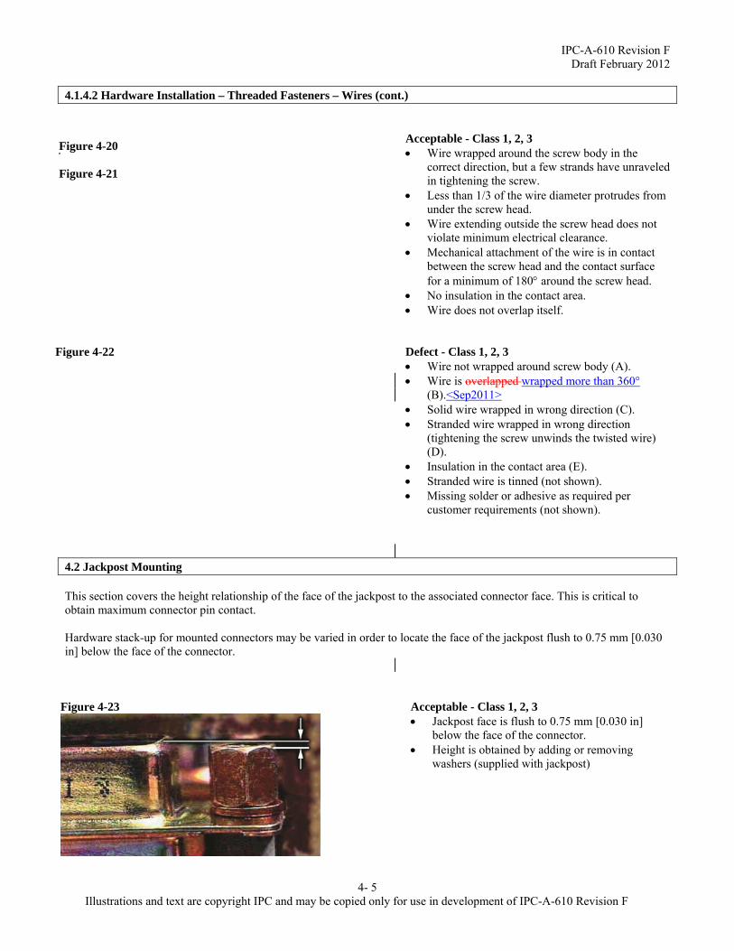
4.2 Jackpost Mounting This section covers the height relationship of the face of the jackpost to the associated connector face. This is critical to obtain maximum connector pin contact. Hardware stack-up for mounted connectors may be varied in order to locate the face of the jackpost flush to 0.75 mm [0.030 in] below the face of the connector.
Acceptable - Class 1, 2, 3 Jackpost face is flush to 0.75 mm [0.030 in]
below the face of the connector. Height is obtained by adding or removing
washers (supplied with jackpost)
Figure 4-20 Figure 4-21
Figure 4-22
Figure 4-23

IPC-A-610 Revision F Draft February 2012
4- 6 Illustrations and text are copyright IPC and may be copied only for use in development of IPC-A-
610 Revision F
Defect - Class 1, 2, 3 Jackpost face extends above the connector face
(Figure 4-24). Face of jackpost is greater than 0.75 mm [0.030
in] below the connector face (Figure 4-25).
4.3 Connector Pins This section covers two types of pin installations; edge connector pins and connector pins. Installation of these devices is usually done with automated equipment. Visual inspection of this mechanical operation includes: correct pins, damaged pins, bent and broken pins, damaged spring contacts and damage to the substrate or conductive pattern. For connector mounting criteria see 7.1.8. For connector damage criteria see 9.5. 4.3.1 Connector Pins - Edge Connector Pins
Acceptable - Class 1, 2, 3 Gap is within specified tolerance. Contact is contained within the insulator. Note: To provide allowance for an extraction tool, the gap between the contact shoulder and the land needs to be adequate for each manufacturer's repair tooling. Defect - Class 1, 2, 3 Contact is above insulator (A). Gap between contact shoulder and land is greater
than specified (B).
4.3.2 Connector Pins - Press Fit Pins
Target – Class 1, 2, 3 Pins are straight, not twisted and properly seated. Acceptable - Class 1, 2, 3 Pins are bent off center by 50% pin thickness or
less. Note: Nominal height tolerance is per pin connector or master drawing specification. The connector pins and mating connector must have a good electrical contact.
Figure 4-24 Figure 4-25
Figure 4-26 1. Backplane 2. Land 3. Shoulder 4. Contact 5. Gap 6. No land damage 7. No discernible damage 8. Insulator
Figure 4-27
Figure 4-28 1. No discernible damage 2. Land 3. No discernible twist
Figure 4-29 1. Pin height tolerance 2. Less than 50% pin thickness

IPC-A-610 Revision F Draft February 2012
4- 7 Illustrations and text are copyright IPC and may be copied only for use in development of IPC-A-
610 Revision F
Defect - Class 1, 2, 3 Pin is bent out of alignment. (Pin is bent off
center greater than 50% pin thickness.) Pin visibly twisted. Pin height is out of tolerance as to specification. Acceptable – Class 1, 2, 3 No lifted or fractured annular rings with press fit
pins. Acceptable - Class 1, 2 Protrusion side land lifted less than or equal to
75% of the width (W) of the annular ring, figure 4-33.
Acceptable – Class 2 No visual evidence of lifted land on insertion side. Acceptable – Class 3 No lifted or fractured annular rings. Defect - Class 1, 2 Any protrusion side functional land lifted more
than 75% of the width (W). Defect – Class 2 Any evidence of lifted lands on the insertion side. Defect - Class 3 Any lifted or fractured annular rings with press fit
pins. Note: For additional information see 10.3.2 Conductor/Land Damage - Lifted Pads/Lands.
4.3.2.1 Press Fit Pins - Soldering The term “press fit pins” is generic in nature and many types of pressure inserted pins, e.g. connector, staked, etc., are not intended to be soldered. If soldering is required the following criteria is applicable.
Target - Class 1, 2, 3 A 360 solder fillet is evident on the secondary
side of the assembly. Note: Solder fillet or fill on primary side is not required.
Figure 4-30 Figure 4-31 Figure 4-32
Figure 4-33 1. Land lifted 75% or less 2. Land with conductor 3. Land not fractured 4. Land lifted, fractured but firmly attached land without conductor (nonfunctional)
Figure 4-34 1. Land fractured 2. Functional land lifted greater than 75% of land width 3. Land lifted
Figure 4-35 Figure 4-36 1. Bottom view 2. side view 3. Land 4. Top view 5. PCB

IPC-A-610 Revision F Draft February 2012
4- 8 Illustrations and text are copyright IPC and may be copied only for use in development of IPC-A-
610 Revision F
Acceptable - Class 1, 2 Solder fillet or coverage (secondary side) is
present on two adjacent sides of the pin. Acceptable – Class 3 A 330 solder fillet is evident on the secondary
side of the assembly. Acceptable - Class 1 Solder wicking is permitted above 2.5 mm
[0.0984 in] on sides of pins provided there is no solder build up which interferes with subsequent attachments to the pin.
Acceptable - Class 2, 3 Solder wicking on sides of pins is less than 2.5
mm [0.0984 in], provided the solder does not interfere with subsequent attachments to the pin.
Defect - Class 1, 2 Solder fillet or coverage is evident on less than 2
adjacent sides of the pin on the secondary side. Defect - Class 3 Less than 330 solder fillet on the secondary side
of the assembly. Defect - Class 1, 2, 3 Solder build up interferes with subsequent
attachments to the pin. Defect - Class 2, 3 Solder wicking exceeds 2.5 mm [0.0984 in].
4.4 Wire Bundle Securing Additional criteria can be found in IPC/WHMA-A-620. 4.4.1 Wire Bundle Securing – General Note: Do not subject wax impregnated lacing tape to cleaning solvents. Beeswax is unacceptable for Class 3.
Target - Class 1, 2, 3 Restraining devices are neat and tight, and
spaced to keep the wires secured in a tight neat bundle.
Figure 4-37 1. Bottom view 2. side view 3. Land 4. Top view 5. PCB
Figure 4-38
Figure 4-39 1. Bottom view 2. side view 3. Land 4. Top view 5. PCB
Figure 4-40

IPC-A-610 Revision F Draft February 2012
4- 9 Illustrations and text are copyright IPC and may be copied only for use in development of IPC-A-
610 Revision F
Acceptable - Class 1, 2, 3 The end of the tie wrap/strap:
Protrudes a maximum of one tie wrap/strap thickness.
Is cut reasonably square to the face of the wrap.
The wires are secured in the wire bundle. Acceptable -- Class 1, 2, 3 Lacing or tie wraps/straps are placed on both
sides of a wire breakout. Spot tie wraps/straps are neat and tight. The wires are secured in the wire bundle. Square knot, surgeons knot or other approved
knot is used to secure the lacing, figure 4-43. Acceptable – Class 1 Process Indicator – Class 2 Defect - Class 3 The wire is under stress at the wrap. Spot ties or wraps/straps are under sleeving or
markers.
4.4.1 Wire Bundle Securing – General (cont.)
Defect - Class 1, 2, 3 Spot tie wrap/strap or knot is loose. Spot tie wrap/strap cuts into the insulation. Wire bundle is loose. Cable tied with an improper knot. This tie may
eventually loosen.
4.4.2 Wire Bundle Securing - Lacing Lacing differs from cable ties because it is a continuous lace. Lacing has closer spacing than cable ties. Criteria for cable ties apply to lacing. Note: Do not subject wax impregnated lacing tape to cleaning solvents. Beeswax is unacceptable for Class 3.
Acceptable - Class 1, 2, 3 Lacing begins and ends with a locking knot. Lacing is tight and wires are kept secure in a neat
bundle.
Figure 4-41
Figure 4-42 Figure 4-43
Figure 4-44
Figure 4-45 1. Loose knot/tie 2. Tie wrap/strap is too tight. Lacing or tie wrap/strap cuts into the insulation 3. Loose bundle Figure 4-46
Figure 4-47
IPC-A-610 Revision F Draft February 2012
4- 10 Illustrations and text are copyright IPC and may be copied only for use in development of IPC-A-
610 Revision F
Defect - Class 1, 2, 3 Lacing is loose, leaving wires loose in the wire
bundle (1). Lacing is too tight, cutting into insulation (2).
4.4.2.1 Wire Bundle Securing - Lacing- Damage
Target – Class 1, 2, 3 Restraining devices are not worn, frayed, nicked,
or broken in any location. Restraining devices do not have sharp edges that
may be a hazard to personnel or equipment. Acceptable – Class 1, 2 Restraining devices exhibit minor fraying, nicks,
or wear of less than 25% of the device thickness. Defect – Class 1, 2 Damage or wear to restraining device greater than
25% of the device thickness (1). Defect – Class 3 Damage or wear to restraining device (1). Cut end of lacing has not been heat seared. Heat searing touches knot. Ends of lacing tape is frayed. Defect – Class 1, 2, 3 Sharp edges that are a hazard to personnel or
equipment (2). Broken lacing ends are not tied off using a square
knot, surgeons knot, or other approved knot (3).
4.5 Routing – Wires and Wire Bundles <Sep2011> These criteria are applicable to single wires or wire bundles. Wires in wire bundles are positioned to minimize crossover and maintain a uniform appearance. 4.5.1 Routing – Wires and Wire Bundles – Wire Crossover
Target - Class 1, 2, 3 Wire lay is essentially parallel to the axis of the
bundle with no crossover. Coaxial cable secured with tie wraps/straps.
Figure 4-48
Figure 4-49
Figure 4-50
Figure 4-51
IPC-A-610 Revision F Draft February 2012
4- 11 Illustrations and text are copyright IPC and may be copied only for use in development of IPC-A-
610 Revision F
Acceptable – Class 1, 2, 3 Wires twist and crossover, but bundle is
essentially uniform in diameter. Acceptable - Class 1 Process Indicator –Class 2 Defect – Class 3 Wires twist and crossover underneath a tie
wrap/strap. Acceptable - Class 1 Defect -Class 2, 3 Bundle is not uniform in diameter. Excessive crossover. Defect -Class 1, 2, 3 Any kinks that violate minimum bend radius. Wire insulation is damaged (see 6.2.1).
4.5.2 Routing – Wires and Wire Bundles – Bend Radius Bend radius is measured along the inside curve of the wire or wire bundles. Table 4-1 Minimum Bend Radius Requirements
Cable Type Class 1 Class 2 Class 3 Bare bus or enamel insulated wire
2X OD1 2X OD1 2X OD1
Insulated wire and flat ribbon cable
2X OD1 2X OD1 2X OD1
Cable bundles with no coax cables
2X OD1 2X OD1 2X OD1
Cable bundles with coax cables
5X OD1 5X OD1 5X OD1
Coaxial cables <Sep2011> 5X OD1 5X OD1 5X OD1 CAT 5 Ethernet cable 4X OD1 4X OD1 4X OD1 Fiber Optic Cable – Buffered and Jacketed Single Fiber
2.54 cm [1 in] or as specified by the manufacturer
2.54 cm [1 in] or as specified by the manufacturer
2.54 cm [1 in] or as specified by the manufacturer
Larger jacketed fibers 15X cable diameter or as specified by the
manufacturer
15X cable diameter or as specified by the manufacturer
15X cable diameter or as specified by the manufacturer
Coaxial Fixed Cable2 5X OD1 5X OD1 5X OD1 Coaxial Flexible Cable23 10X OD1 10X OD1 10X OD1
Unshielded Wires No Requirement Established 3X for ≤ AWG 10 5X for >AWG 10
Shielded Wires and Cables No Requirement Established 5X OD1 Semirigid Coax Not less than manufacturer’s stated minimum bend radius
Harness assembly Bend radius is equal to or greater than the minimum bend radius of any individual wire/cable
within the harness. Note 1: OD is the outer diameter of the wire or cable, including insulation. Note 2: Coaxial Fixed Cable - Coaxial cable that is secured to prevent movement; not expected to have the cable repeatedly flexed during operation of the equipment.
Figure 4-52
Figure 4-53

IPC-A-610 Revision F Draft February 2012
4- 12 Illustrations and text are copyright IPC and may be copied only for use in development of IPC-A-610 Revision F
Note 3: Coaxial Flexible Cable - Coaxial cable that is or may be flexed during operation of the equipment. Acceptable – Class 1, 2, 3 Minimum bend radius meets requirements of Table 4-1. Defect – Class 1, 2, 3 Bend radius is less than the minimum bend radius requirements of Table 4-1. 4.5.3 Routing – Wires and Wire Bundles – Coaxial Cable
Acceptable - Class 1, 2, 3 Inside bend radius meets the criteria of Table 4-1. Defect - Class 1, 2, 3 Inside bend radius does not meet the criteria of Table 4-1. Defect - Class 3 Tie wraps/straps that cause any deformation of coaxial
cables.
4.5.4 Routing – Wires and Wire Bundles – Unused Wire Termination
Target - Class 1, 2, 3 Sleeving extends three wire diameters past end of wire. Unused wire is folded back and tied into the wire bundle. Acceptable - Class 1, 2, 3 Ends of unused wires are covered with shrink sleeving. Wire may extend straight down length of bundle (Figure
4-56) or be folded back (Figure 4-57). Sleeving extends at least 2 wire diameters beyond end of
wire. Sleeving extends onto the wire insulation for a minimum
of 4 wire diameters or 6 mm [0.24 in], whichever is greater.
Unused wire is tied into the wire bundle. Process Indicator - Class 2 Defect - Class 3 Insulating sleeving extends beyond end of wire less than
two wire diameters. Insulating sleeving extends onto wire insulation less than
4 wire diameters or 6 mm [0.24 in], whichever is greater. Defect - Class 1, 2, 3 Ends of unused wires are exposed. Unused wire is not tied into the wire bundle.
Figure 4-54
Figure 4-55
Figure 4-56 IPC ACTION TO ADD KEYS TO FIGURES AND BULLETS
Figure 4-57 IPC ACTION TO ADD KEYS TO FIGURES AND BULLETS
Figure 4-58
IPC-A-610 Revision F Draft February 2012
4- 13 Illustrations and text are copyright IPC and may be copied only for use in development of IPC-A-610 Revision F
4.5.5 Routing – Wires and Wire Bundles – Ties over Splices and Ferrules
Acceptable - Class 1, 2, 3 Tie wraps/straps are placed near splices or solder ferrules
contained in the wire bundle. No stress on wires exiting splices. Acceptable - Class 1 Process Indicator – Class 2 Defect – Class 3 Tie wraps/straps are placed over splices or solder ferrules
contained in the wire bundle. Defect-Class 1, 2, 3 Tie wrap/strap is placing stress on the wire(s) exiting the
splice.
Figure 4-59
Figure 4-60
Figure 4-61
IPC-A-610 Revision F Draft February 2012
5-1 Illustrations and text are copyright IPC and may be copied only for use in development of IPC-A-610 Revision F
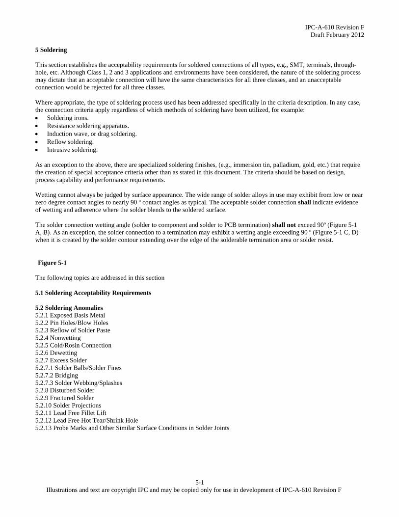
5 Soldering This section establishes the acceptability requirements for soldered connections of all types, e.g., SMT, terminals, through-hole, etc. Although Class 1, 2 and 3 applications and environments have been considered, the nature of the soldering process may dictate that an acceptable connection will have the same characteristics for all three classes, and an unacceptable connection would be rejected for all three classes. Where appropriate, the type of soldering process used has been addressed specifically in the criteria description. In any case, the connection criteria apply regardless of which methods of soldering have been utilized, for example: Soldering irons. Resistance soldering apparatus. Induction wave, or drag soldering. Reflow soldering. Intrusive soldering. As an exception to the above, there are specialized soldering finishes, (e.g., immersion tin, palladium, gold, etc.) that require the creation of special acceptance criteria other than as stated in this document. The criteria should be based on design, process capability and performance requirements. Wetting cannot always be judged by surface appearance. The wide range of solder alloys in use may exhibit from low or near zero degree contact angles to nearly 90 º contact angles as typical. The acceptable solder connection shall indicate evidence of wetting and adherence where the solder blends to the soldered surface. The solder connection wetting angle (solder to component and solder to PCB termination) shall not exceed 90º (Figure 5-1 A, B). As an exception, the solder connection to a termination may exhibit a wetting angle exceeding 90 º (Figure 5-1 C, D) when it is created by the solder contour extending over the edge of the solderable termination area or solder resist.
The following topics are addressed in this section 5.1 Soldering Acceptability Requirements 5.2 Soldering Anomalies 5.2.1 Exposed Basis Metal 5.2.2 Pin Holes/Blow Holes 5.2.3 Reflow of Solder Paste 5.2.4 Nonwetting 5.2.5 Cold/Rosin Connection 5.2.6 Dewetting 5.2.7 Excess Solder 5.2.7.1 Solder Balls/Solder Fines 5.2.7.2 Bridging 5.2.7.3 Solder Webbing/Splashes 5.2.8 Disturbed Solder 5.2.9 Fractured Solder 5.2.10 Solder Projections 5.2.11 Lead Free Fillet Lift 5.2.12 Lead Free Hot Tear/Shrink Hole 5.2.13 Probe Marks and Other Similar Surface Conditions in Solder Joints
Figure 5-1

IPC-A-610 Revision F Draft February 2012
5-2 Illustrations and text are copyright IPC and may be copied only for use in development of IPC-A-610 Revision F
5.1 Soldering Acceptability Requirements See 5.2 for examples of soldering anomalies.
Target – Class 1, 2, 3 Solder fillet appears generally smooth and exhibits
good wetting of the solder to the parts being joined. Outline of the parts is easily determined. Solder at the lead being joined creates a feathered
edge. Fillet is concave in shape. Acceptable - Class 1, 2, 3 There are materials and processes, e.g. lead free
alloys and slow cooling with large mass PCBs, that may produce dull matte, gray, or grainy appearing solders that are normal for the material or process involved. These solder connections are acceptable.
The solder connection wetting angle (solder to component and solder to PCB termination) do not exceed 90º (Figure 5-1 A, B). - As an exception, the solder connection to a
termination may exhibit a wetting angle exceeding 90 º (Figure 5-1 C, D) when it is created by the solder contour extending over the edge of the solderable termination area or solder resist.
The primary difference between the solder connections created with processes using tin-lead alloys and processes using lead free alloys is related to the visual appearance of the solder. This standard provides visual criteria for inspection of both tin-lead and lead-free connections. In this Standard, figures specific to lead-free connections will be identified with the symbol shown in Figure 5-3. Acceptable lead-free and tin-lead connections may exhibit similar appearances but lead free alloys are more likely to have surface roughness (grainy or dull) or greater wetting contact angles. Solder fillet criteria for SnPb and lead-free alloys are the same. Typical tin-lead connections have from a shiny to a satin luster, generally smooth appearance and exhibit wetting as exemplified by a concave meniscus between the objects being soldered. High temperature solders may have a dull appearance. Touch-up (rework) of soldered connections is performed with discretion to avoid causing additional problems, and to produce results that exhibit the acceptability criteria of the applicable class.
Figure 5-2 Figure 5-3
IPC-A-610 Revision F Draft February 2012
5- 3
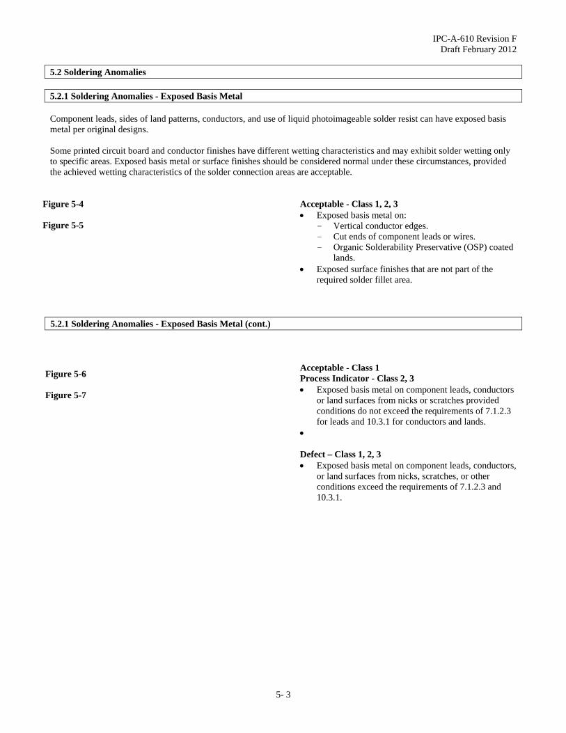
5.2 Soldering Anomalies 5.2.1 Soldering Anomalies - Exposed Basis Metal Component leads, sides of land patterns, conductors, and use of liquid photoimageable solder resist can have exposed basis metal per original designs. Some printed circuit board and conductor finishes have different wetting characteristics and may exhibit solder wetting only to specific areas. Exposed basis metal or surface finishes should be considered normal under these circumstances, provided the achieved wetting characteristics of the solder connection areas are acceptable.
Acceptable - Class 1, 2, 3 Exposed basis metal on:
- Vertical conductor edges. - Cut ends of component leads or wires. - Organic Solderability Preservative (OSP) coated
lands. Exposed surface finishes that are not part of the
required solder fillet area.
5.2.1 Soldering Anomalies - Exposed Basis Metal (cont.)
Acceptable - Class 1 Process Indicator - Class 2, 3 Exposed basis metal on component leads, conductors
or land surfaces from nicks or scratches provided conditions do not exceed the requirements of 7.1.2.3 for leads and 10.3.1 for conductors and lands.
Defect – Class 1, 2, 3 Exposed basis metal on component leads, conductors,
or land surfaces from nicks, scratches, or other conditions exceed the requirements of 7.1.2.3 and 10.3.1.
Figure 5-4 Figure 5-5
Figure 5-6 Figure 5-7

IPC-A-610 Revision F Draft February 2012
5- 4
5.2.2 Soldering Anomalies - Pin Holes/Blow Holes
Acceptable - Class 1 Process Indicator - Class 2, 3 Blowholes (Figures 5-8, 9), pinholes (Figure 5-10),
voids (Figures 5-11, 12), etc., providing the solder connection meets all other requirements.
Defect – Class 1, 2, 3 Solder connections where pin holes, blow holes,
voids, etc. reduce the connections below minimum requirements (not shown).
5.2.3 Soldering Anomalies - Reflow of Solder Paste
Defect - Class 1, 2, 3 Incomplete reflow of solder paste.
5.2.4 Soldering Anomalies - Nonwetting IPC-T-50 defines nonwetting as the inability of molten solder to form a metallic bond with the basis metal. In this Standard, that includes surface finishes, see 5.2.1.
Defect - Class 1, 2, 3 Solder has not wetted to the land or termination
where solder is required. (Figures 5-17, 18, 19 component terminations, Figure 5-20 shield termination, Figure 5-21 wire termination)
Solder coverage does not meet requirements for the termination type.
Figure 5-8 Figure 5-9 Figure 5-10 Figure 5-11 Figure 5-12
Figure 5-13 Figure 5-14 Figure 5-15 Figure 5-16
Figure 5-17 Figure 5-18 Figure 5-19 Figure 5-20 Figure 5-21
IPC-A-610 Revision F Draft February 2012
5- 5
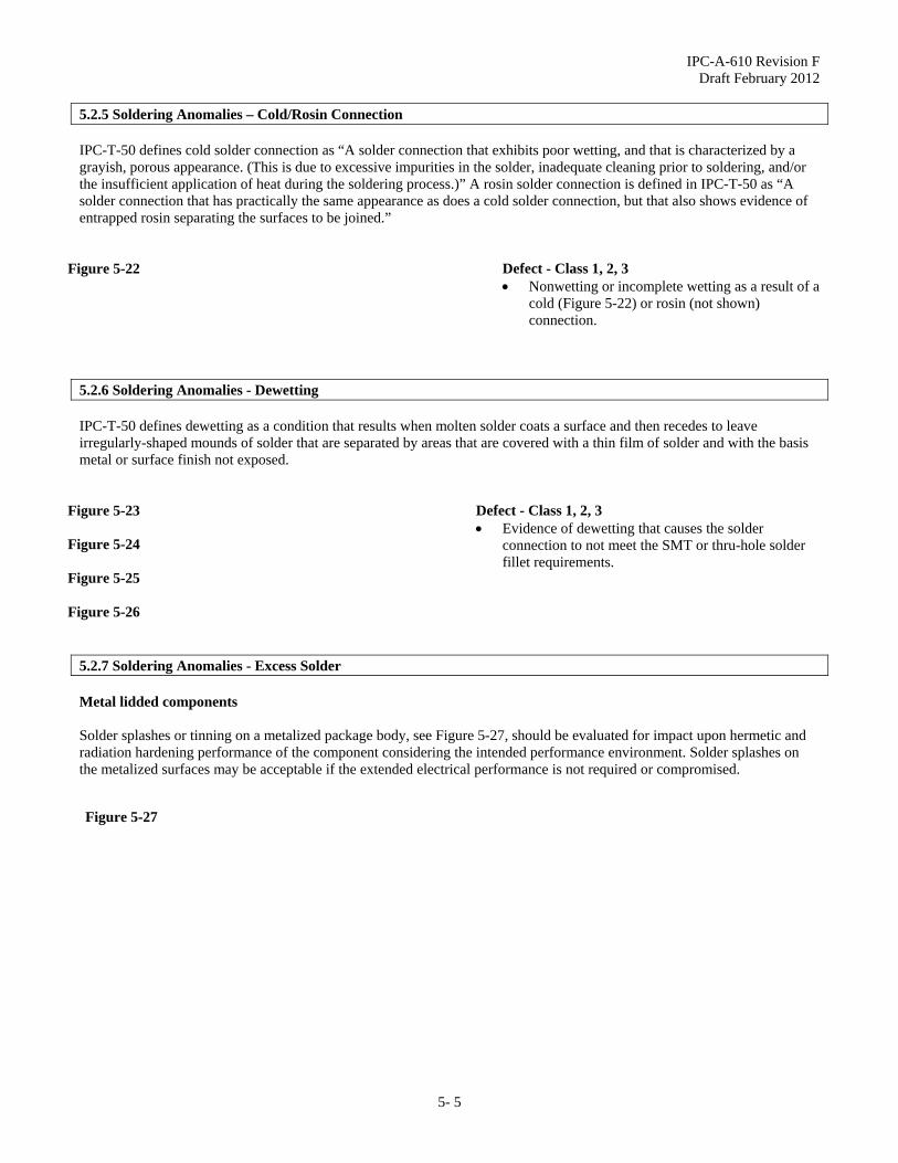
5.2.5 Soldering Anomalies – Cold/Rosin Connection IPC-T-50 defines cold solder connection as “A solder connection that exhibits poor wetting, and that is characterized by a grayish, porous appearance. (This is due to excessive impurities in the solder, inadequate cleaning prior to soldering, and/or the insufficient application of heat during the soldering process.)” A rosin solder connection is defined in IPC-T-50 as “A solder connection that has practically the same appearance as does a cold solder connection, but that also shows evidence of entrapped rosin separating the surfaces to be joined.”
Defect - Class 1, 2, 3 Nonwetting or incomplete wetting as a result of a
cold (Figure 5-22) or rosin (not shown) connection.
5.2.6 Soldering Anomalies - Dewetting IPC-T-50 defines dewetting as a condition that results when molten solder coats a surface and then recedes to leave irregularly-shaped mounds of solder that are separated by areas that are covered with a thin film of solder and with the basis metal or surface finish not exposed.
Defect - Class 1, 2, 3 Evidence of dewetting that causes the solder
connection to not meet the SMT or thru-hole solder fillet requirements.
5.2.7 Soldering Anomalies - Excess Solder Metal lidded components Solder splashes or tinning on a metalized package body, see Figure 5-27, should be evaluated for impact upon hermetic and radiation hardening performance of the component considering the intended performance environment. Solder splashes on the metalized surfaces may be acceptable if the extended electrical performance is not required or compromised.
Figure 5-22
Figure 5-23
Figure 5-24 Figure 5-25 Figure 5-26
Figure 5-27

IPC-A-610 Revision F Draft February 2012
5- 6
5.2.7.1 Soldering Anomalies - Excess Solder- Solder Balls/Solder Fines Solder balls are spheres of solder that remain after the soldering process. Solder fines are typically small balls of the original solder paste metal screen size that have splattered around the connection during the reflow process.
Target – Class 1, 2, 3 No evidence of solder balls on the printed wiring
assembly.
5.2.7.1 Soldering Anomalies - Excess Solder- Solder Balls/Solder Fines (cont.)
Acceptable – Class 1, 2, 3 Solder balls are entrapped, encapsulated or attached
(e.g. in no-clean residue, with conformal coating, soldered to a metal surface, embedded in the solder resist or under a component).
Solder balls do not violate minimum electrical clearance.
Defect - Class 1, 2, 3 Solder balls are not entrapped, encapsulated or
attached or can become dislodged in the normal service environment.
Solder balls violate minimum electrical clearance.
5.2.7.2 Soldering Anomalies - Excess Solder- Bridging
Defect - Class 1, 2, 3 A solder connection across conductors that should
not be joined. Solder has bridged to adjacent noncommon
conductor or component.
Figure 5-28
Figure 5-29
Figure 5-30 Figure 5-31 Figure 5-32 Figure 5-33
Figure 5-34 Figure 5-35 Figure 5-36 Figure 5-37

IPC-A-610 Revision F Draft February 2012
5- 7
5.2.7.3 Soldering Anomalies - Excess Solder- Solder Webbing/Splashes Visual inspection for solder splashes shall be done without magnification.
Target – Class 1, 2, 3 No solder splashes or webbing. Acceptable – Class 1, 2, 3 Solder splashes or metallic particles meet the
following criteria: Attached/entrapped/encapsulated on the PCA
surface or solder mask, or soldered to metallic surface.
Do not violate minimum electrical clearance. Defect - Class 1, 2, 3 Solder webbing. Solder splashes that are not attached, entrapped,
encapsulated. Solder splashes on metal component surfaces impact
form, fit or function, e.g. damages lid seal on hermetic components.
Violate minimum electrical clearance. Note: Entrapped/encapsulated/attached is intended to mean that normal service environment of the product will not cause solder to become dislodged.
5.2.8 Soldering Anomalies - Disturbed Solder Surface appearance with cooling lines as shown in Acceptable Figures 5-40 (lead free) and 5-41 (SnPb) are more likely to occur in lead free alloys and are not a disturbed solder condition.
Acceptable - Class 1, 2, 3 Lead free and tin-lead solder connections exhibit:
Cooling lines, Figure 5-40. Secondary reflow Figure 5-41.
Defect - Class 1, 2, 3 Disturbed solder joint characterized by uneven
surface from movement in the solder connection during cooling.
Figure 5-38 Figure 5-39
Figure 5-40 Figure 5-41
Figure 5-42 Figure 5-43
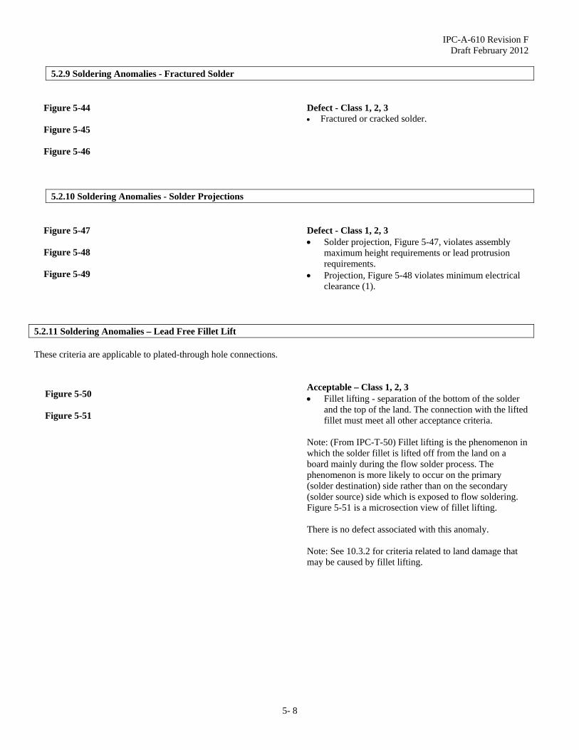
IPC-A-610 Revision F Draft February 2012
5- 8
5.2.9 Soldering Anomalies - Fractured Solder
Defect - Class 1, 2, 3 Fractured or cracked solder.
5.2.10 Soldering Anomalies - Solder Projections
Defect - Class 1, 2, 3 Solder projection, Figure 5-47, violates assembly
maximum height requirements or lead protrusion requirements.
Projection, Figure 5-48 violates minimum electrical clearance (1).
5.2.11 Soldering Anomalies – Lead Free Fillet Lift These criteria are applicable to plated-through hole connections.
Acceptable – Class 1, 2, 3 Fillet lifting - separation of the bottom of the solder
and the top of the land. The connection with the lifted fillet must meet all other acceptance criteria.
Note: (From IPC-T-50) Fillet lifting is the phenomenon in which the solder fillet is lifted off from the land on a board mainly during the flow solder process. The phenomenon is more likely to occur on the primary (solder destination) side rather than on the secondary (solder source) side which is exposed to flow soldering. Figure 5-51 is a microsection view of fillet lifting. There is no defect associated with this anomaly. Note: See 10.3.2 for criteria related to land damage that may be caused by fillet lifting.
Figure 5-44 Figure 5-45 Figure 5-46
Figure 5-47 Figure 5-48 Figure 5-49
Figure 5-50 Figure 5-51

IPC-A-610 Revision F Draft February 2012
5- 9
5.2.12 Soldering Anomalies – Lead Free Hot Tear/Shrink Hole There is no defect associated with this anomaly provided the connection meets all other acceptance criteria. Figures 5-52 and 5-53 are examples of hot tear.
5.2.13 Probe Marks and Other Similar Surface Conditions in Solder Joints
Target – Class 1, 2, 3 The solder joint is free of any probe marks and
other similar surface conditions. Acceptable – Class 1, 2, 3 Probe marks and other similar surface conditions
that do not violate other requirements. Defect – Class 1, 2, 3 Probe marks and other similar surface conditions
cause damage in excess of requirements.
Figure 5-52 Figure 5-53
Figure 5-54
Figure 5-55
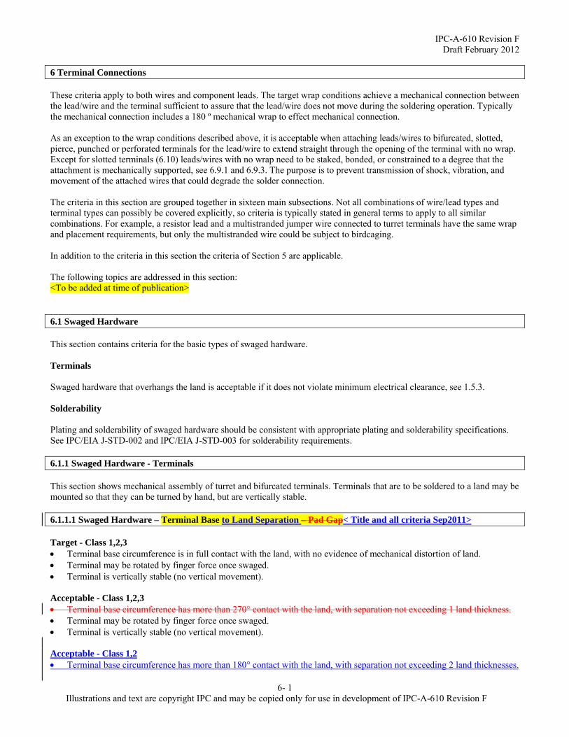
IPC-A-610 Revision F Draft February 2012
6- 1 Illustrations and text are copyright IPC and may be copied only for use in development of IPC-A-610 Revision F
6 Terminal Connections These criteria apply to both wires and component leads. The target wrap conditions achieve a mechanical connection between the lead/wire and the terminal sufficient to assure that the lead/wire does not move during the soldering operation. Typically the mechanical connection includes a 180 º mechanical wrap to effect mechanical connection. As an exception to the wrap conditions described above, it is acceptable when attaching leads/wires to bifurcated, slotted, pierce, punched or perforated terminals for the lead/wire to extend straight through the opening of the terminal with no wrap. Except for slotted terminals (6.10) leads/wires with no wrap need to be staked, bonded, or constrained to a degree that the attachment is mechanically supported, see 6.9.1 and 6.9.3. The purpose is to prevent transmission of shock, vibration, and movement of the attached wires that could degrade the solder connection. The criteria in this section are grouped together in sixteen main subsections. Not all combinations of wire/lead types and terminal types can possibly be covered explicitly, so criteria is typically stated in general terms to apply to all similar combinations. For example, a resistor lead and a multistranded jumper wire connected to turret terminals have the same wrap and placement requirements, but only the multistranded wire could be subject to birdcaging. In addition to the criteria in this section the criteria of Section 5 are applicable. The following topics are addressed in this section: <To be added at time of publication> 6.1 Swaged Hardware This section contains criteria for the basic types of swaged hardware. Terminals Swaged hardware that overhangs the land is acceptable if it does not violate minimum electrical clearance, see 1.5.3. Solderability Plating and solderability of swaged hardware should be consistent with appropriate plating and solderability specifications. See IPC/EIA J-STD-002 and IPC/EIA J-STD-003 for solderability requirements. 6.1.1 Swaged Hardware - Terminals This section shows mechanical assembly of turret and bifurcated terminals. Terminals that are to be soldered to a land may be mounted so that they can be turned by hand, but are vertically stable. 6.1.1.1 Swaged Hardware – Terminal Base to Land Separation – Pad Gap< Title and all criteria Sep2011> Target - Class 1,2,3 Terminal base circumference is in full contact with the land, with no evidence of mechanical distortion of land. Terminal may be rotated by finger force once swaged. Terminal is vertically stable (no vertical movement). Acceptable - Class 1,2,3 Terminal base circumference has more than 270° contact with the land, with separation not exceeding 1 land thickness. Terminal may be rotated by finger force once swaged. Terminal is vertically stable (no vertical movement). Acceptable - Class 1,2 Terminal base circumference has more than 180° contact with the land, with separation not exceeding 2 land thicknesses.

IPC-A-610 Revision F Draft February 2012
6- 2 Illustrations and text are copyright IPC and may be copied only for use in development of IPC-A-610 Revision F
Acceptable - Class 3 Terminal base circumference has more than 270° contact with the land, with separation not exceeding 1 land thickness. Defect - Class 1,2 Terminal base circumference has more less than 180° but less than 270° contact with the land., with separation not
exceeding 2 land thicknesses. Terminal base has separation exceeding 2 land thicknesses. Defect – Class 3 Terminal base circumference has less than 270° contact with the land. Terminal base has separation exceeding 1 land thickness. Defect - Class 1,2,3 Terminal is not vertically stable.

IPC-A-610 Revision F Draft February 2012
6- 3 Illustrations and text are copyright IPC and may be copied only for use in development of IPC-A-610 Revision F
6.1.1.2 Swaged Hardware – Terminals - Turret
Target – Class 1,2,3 Terminal intact and straight. Acceptable - Class 1,2,3 Terminal is bent, but the top edge (1) does not
extend beyond the base (2). Acceptable - Class 1 Defect - Class 2,3 The top edge of the terminal is bent beyond the
edge of the base. Defect - Class 1,2,3 The center post is fractured.
6.1.1.3 Swaged Hardware – Terminals - Bifurcated
Target – Class 1,2,3 Terminal intact and straight. Acceptable - Class 1 Defect - Class 2,3 A post is broken, but sufficient mounting area
remains to attach the specified wires/leads. Defect - Class 1,2,3 Both posts are broken.
6.1.2 Swaged Hardware – Rolled Flange The rolled flange terminal is used for mechanical attachments where electrical attachment to a land is not required. Rolled flange attachments are not soldered to a PCB land pattern or installed on active circuitry. They may be installed on inactive and isolated circuitry.
Figure 6-1
Figure 6-2
Figure 6-3
Figure 6-4
Figure 6-5
Figure 6-6 new
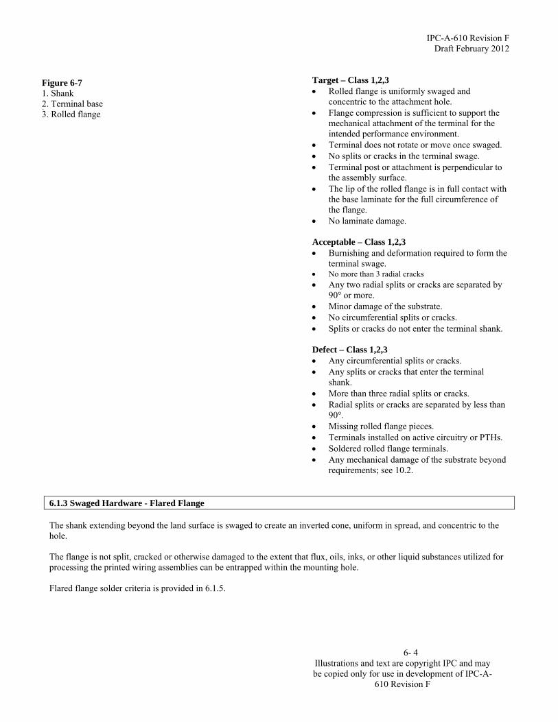
IPC-A-610 Revision F Draft February 2012
6- 4 Illustrations and text are copyright IPC and may be copied only for use in development of IPC-A-
610 Revision F
Target – Class 1,2,3 Rolled flange is uniformly swaged and
concentric to the attachment hole. Flange compression is sufficient to support the
mechanical attachment of the terminal for the intended performance environment.
Terminal does not rotate or move once swaged. No splits or cracks in the terminal swage. Terminal post or attachment is perpendicular to
the assembly surface. The lip of the rolled flange is in full contact with
the base laminate for the full circumference of the flange.
No laminate damage. Acceptable – Class 1,2,3 Burnishing and deformation required to form the
terminal swage. No more than 3 radial cracks Any two radial splits or cracks are separated by
90° or more. Minor damage of the substrate. No circumferential splits or cracks. Splits or cracks do not enter the terminal shank. Defect – Class 1,2,3 Any circumferential splits or cracks. Any splits or cracks that enter the terminal
shank. More than three radial splits or cracks. Radial splits or cracks are separated by less than
90°. Missing rolled flange pieces. Terminals installed on active circuitry or PTHs. Soldered rolled flange terminals. Any mechanical damage of the substrate beyond
requirements; see 10.2.
6.1.3 Swaged Hardware - Flared Flange The shank extending beyond the land surface is swaged to create an inverted cone, uniform in spread, and concentric to the hole. The flange is not split, cracked or otherwise damaged to the extent that flux, oils, inks, or other liquid substances utilized for processing the printed wiring assemblies can be entrapped within the mounting hole. Flared flange solder criteria is provided in 6.1.5.
Figure 6-7 1. Shank 2. Terminal base 3. Rolled flange
IPC-A-610 Revision F Draft February 2012
6- 5 Illustrations and text are copyright IPC and may be copied only for use in development of IPC-A-
610 Revision F
Target – Class 1,2,3 Flared flange is uniformly swaged and
concentric to the hole. Strain or stress marks caused by flaring are kept
to a minimum. The flange is swaged sufficiently tight to prevent
movement in the Z-axis. Acceptable - Class 1,2,3 Split in flared flange does not enter into the
barrel. Not more than three radial splits. Radial splits or cracks are separated by at least
90º. Acceptable - Class 1 Split in flared flange in barrel acceptable if
soldered after swaging. Defect - Class 1,2,3 Flared flange periphery uneven or jagged. Split enters into barrel; see Class 1 exception
above. Any circumferential splits/cracks. More than three radial splits. Radial splits or cracks are separated by less than
90°. Missing flared flange pieces.
6.1.4 Swaged Hardware - Controlled Split This form of swaged hardware is obtained by using scored hardware with a number of uniform segments. When swaged, each segment should conform to a particular angle. Controlled split hardware is to be soldered as soon as possible after swaging to avoid oxidation.
Target – Class 1,2,3 Flange is uniformly split and concentric to the
hole. Split segments do not extend to the outside
diameter of the land. Flange is swaged sufficiently tight to prevent
movement in the z-axis.
Figure 6-8
Figure 6-9
Figure 6-10
Figure 6-11 IPC ACTION TO ADD ARROW POINTING TO CRACK
Figure 6-12

IPC-A-610 Revision F Draft February 2012
6- 6 Illustrations and text are copyright IPC and may be copied only for use in development of IPC-A-
610 Revision F
Acceptable - Class 1,2,3 Flange splits down to the board but not into the
barrel. Defect - Class 1,2,3 Flange damaged. Segments excessively deformed. Segment missing. Split enters into barrel. Circumferential splits/cracks.
6.1.5 Swaged Hardware – Solder These solder acceptance criteria, summarized in Table 6-1, are applicable to flared flange and flat set swaged hardware. The flat set flange is not split, cracked or otherwise damaged to the extent that flux, oils, inks, or other liquid substances utilized for processing the printed board can be entrapped within the mounting hole. Table 6-1 Swaged Hardware Soldering Requirements
Criteria Class 1 Class 2 Class 3
A. Circumferential fillet and wetting - solder source side.
270° 270° 330°
B. Percentage of solder source side land area covered with wetted solder.
75% 75% 75%
C. Height of solder on flared flange. 75% 75% 75%
D. Height of solder on flat set flange. 100% 100% 100%
Target – Class 1,2,3 360° fillet and wetting flange to land. The swaged flange is as close to the land as possible
to prevent movement in the Z axis. Evidence of solder flow is discernible between
swaged flange and land of the printed board or other substrate.
Acceptable – Class 1,2,3 <Sep2011> 75% or more of the land area is covered with wetted
solder. Solder fillet is at least 75% of flare flange height. Solder fillet is 100% of flat set flange height. Acceptable - Class 1,2 Minimum of 270º fillet and wetting flange to land. Any radial split is filled with solder. Solder fillet is at least 75% of flange height.
Figure 6-13
Figure 6-14 Figure 6-15
Figure 6-16
Figure 6-17

IPC-A-610 Revision F Draft February 2012
6- 7 Illustrations and text are copyright IPC and may be copied only for use in development of IPC-A-610
Revision F
Acceptable - Class 3 Minimum of 330º filet and wetting flange to land. No radial or circumferential splits. Solder fillet is at least 75% of flange height. Defect – Class 1,2 Less than 270º fillet and wetting flange or eyelet to
land. Any radial split not filled with solder. Defect - Class 1,2,3 Improperly swaged, flange not seated on terminal
area. Solder fillet is not 75% of flared flange height. Solder fillet is not or 100% of flat set flangeeyelet
height. Less than 75% of the land area is covered with
wetted solder. Defect - Class 3 Solder is less than 330º around flange.
6.2 Insulation 6.2.1 Insulation – Damage 6.2.1.1 Insulation – Damage – Presolder Coatings added over insulation base material such as resin coatings over polyimide are not considered to be part of the insulation and these criteria are not intended to be applicable to those coatings.
Target – Class 1,2,3 Insulation has been trimmed neatly with no signs
of pinching, pulling, fraying, discoloration, charring or burning.
Acceptable - Class 1,2,3 A slight, uniform impression in the insulation
from the gripping of mechanical strippers. Chemical solutions, paste, and creams used to
strip solid wires do not cause degradation to the wire.
Slight discoloration of insulation resulting from thermal processing is permissible, provided it is not charred, cracked or split.
Figure 6-18
Figure 6-19
Figure 6-20

IPC-A-610 Revision F Draft February 2012
6- 8 Illustrations and text are copyright IPC and may be copied only for use in development of IPC-A-
610 Revision F
Defect – Class 1,2,3 Any cuts, breaks, cracks or splits in insulation
(not shown). Insulation is melted into the wire strands (not
shown). Insulation thickness is reduced by more than
20% (Figures 6-21, 6-22). Uneven or ragged pieces of insulation (frays,
tails, and tags) are greater than 50% of the wire diameter or 1 mm [0.039 in] whichever is more (Figure 6-23).
Insulation is charred (Figure 6-24).
6.2.1.2 Insulation – Damage – Post-Solder
Target – Class 1,2,3 Insulation is not melted, charred or otherwise
damaged from the soldering process. Acceptable - Class 1,2,3 Slight melting of insulation. Defect - Class 1,2,3 Insulation charred. Solder connection contaminated by burnt or
melted insulation.
6.2.2 Insulation - Clearance
Target – Class 1,2,3 There is an insulation clearance (C) of one wire
diameter (D) between the end of the insulation and the solder fillet.
Acceptable – Class 1,2,3 The insulation clearance (C) is two wire
diameters or less including insulation or 1.5mm [0.0591 in] (whichever is greater).
Insulation clearance (C) does not permit violation of minimum electrical clearance to adjacent noncommon conductors.
The insulation is in contact with the solder but does not interfere with formation of an acceptable connection.
Figure 6-21 Figure 6-22 Figure 6-23 Figure 6-24
Figure 6-25
Figure 6-26
Figure 6-27
Figure 6-28
Figure 6-29 Figure 6-30

IPC-A-610 Revision F Draft February 2012
6- 9 Illustrations and text are copyright IPC and may be copied only for use in development of IPC-A-
610 Revision F
Acceptable – Class 1 Exposed bare wire providing there is no danger
of violating minimum electrical clearance to adjacent noncommon circuitry when the wire is moved.
Acceptable – Class 1 Process Indicator – Class 2 Defect – Class 3 The insulation clearance (C) is greater than two
wire diameters including insulation or 1.5 mm [0.0591 in], whichever is greater.
Defect – Class 1,2,3 Insulation clearance (C) permits violation of
minimum electrical clearance to adjacent noncommon conductors.
Insulation interferes with formation of the solder connection.
Defect – Class 2,3 Insulation is embedded in or covered with solder.
6.2.3 Insulation - Flexible Sleeve 6.2.3.1 Insulation - Flexible Sleeve - Placement
Target – Class 1,2,3 Insulation sleeving overlaps the connector
terminal and extends over the wire insulation four wire diameters (D).
Insulation sleeving is one wire diameter (D) from the point where the connector terminal enters the connector insert.
Acceptable – Class 1,2,3 Insulation sleeving overlaps the connector
terminal and the wire insulation by a minimum of two wire diameters.
Insulation sleeving is more than 50% wire diameter and not more than 2 wire diameters from the point where the connector terminal enters the connector insert.
Acceptable – Class 1 Sleeving/tubing is tight on terminal, but not tight
on wire/cable.
Figure 6-31
Figure 6-32
Figure 6-33
Figure 6-34
IPC-A-610 Revision F Draft February 2012
6- 10 Illustrations and text are copyright IPC and may be copied only for use in development of IPC-A-
610 Revision F
Acceptable – Class 2,3 Sleeving/tubing is tight on terminal and
wire/cable.<Sep2011> Sleeving/tubing is tight on wire/cable. Multiple pieces of sleeving overlap each other by
at least 3 wire/cable diameters, or 13 mm [0.5 inch], whichever is larger.
Defect – Class 1 Sleeving/tubing is not tight on terminal. and not
tight on wire/cable. Defect – Class 2,3 Sleeving/tubing is not tight on terminal and
wire/cable. Sleeving/tubing is not tight on wire/cable. Multiple pieces of sleeving overlap is less than 3
wire/cable diameters or 13 mm [0.5 inch,], or less than 3 wire/cable diameters, whichever is less.
Defect – Class 1,2,3 Insulation sleeving overlaps the wire insulation
by less than two wire diameters, Figure 6-35A. Insulation sleeving is more than two wire
diameters from the point where the connector terminal enters the connector insert, Figure 6-35B.
Insulation sleeve is loose on the terminal (could slide or vibrate off, exposing more than the allowed amount of conductor or terminal) , Figure 6-35C.
Insulation sleeving prevents movement of floating contact in the insert, when movement is required.
6.2.3.2 Insulation - Flexible Sleeve - Damage
Acceptable – Class 1,2,3 No damage to insulation sleeving, i.e. splits, char, cracks, tears or pinholes. Defect – Class 1,2,3 Insulation sleeving is damaged, i.e. splits, char,
cracks, tears or pinholes.
Figure 6-35
Figure 6-36 Figure 6-37

IPC-A-610 Revision F Draft February 2012
6- 11 Illustrations and text are copyright IPC and may be copied only for use in development of IPC-A-610 Revision F
6.3 Conductor 6.3.1 Conductor - Deformation
Target – Class 1,2,3 Strands are not flattened, untwisted, buckled,
kinked or otherwise deformed. Acceptable - Class 1,2,3 Where strands were straightened during the
insulation removal, they have been restored to approximate the original spiral lay of the strands.
Wire strands are not kinked. Acceptable – Class 1 Defect – Class 2,3 The general spiral lay of the strands has not been
maintained.
6.3.2 Conductor – Strand Damage
Target – Class 1,2,3 Wire strands are not scraped, nicked, cut,
flattened, scored, or otherwise damaged. Acceptable - Class 1 Process Indicator - Class 2,3 Strands cut, broken, scraped or severed if the
number of damaged or broken strands in a single wire does not exceed the limits in Table 6-2.
Defect - Class 1,2,3 The number of damaged (scraped, nicked or
severed) strands in a single wire exceeds the limits in Table 6-2.
Figure 6-38
Figure 6-39
Figure 6-40
Figure 6-41 Figure 6-42
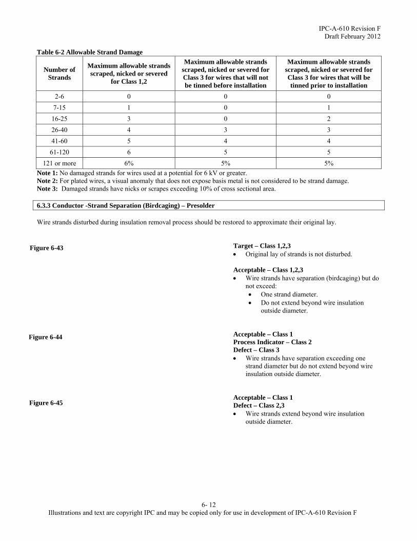
IPC-A-610 Revision F Draft February 2012
6- 12 Illustrations and text are copyright IPC and may be copied only for use in development of IPC-A-610 Revision F
Table 6-2 Allowable Strand Damage
Number of Strands
Maximum allowable strands scraped, nicked or severed
for Class 1,2
Maximum allowable strands scraped, nicked or severed for Class 3 for wires that will not be tinned before installation
Maximum allowable strands scraped, nicked or severed for Class 3 for wires that will be tinned prior to installation
2-6 0 0 0
7-15 1 0 1
16-25 3 0 2
26-40 4 3 3
41-60 5 4 4
61-120 6 5 5
121 or more 6% 5% 5%
Note 1: No damaged strands for wires used at a potential for 6 kV or greater. Note 2: For plated wires, a visual anomaly that does not expose basis metal is not considered to be strand damage. Note 3: Damaged strands have nicks or scrapes exceeding 10% of cross sectional area. 6.3.3 Conductor -Strand Separation (Birdcaging) – Presolder Wire strands disturbed during insulation removal process should be restored to approximate their original lay.
Target – Class 1,2,3 Original lay of strands is not disturbed. Acceptable – Class 1,2,3 Wire strands have separation (birdcaging) but do
not exceed: One strand diameter. Do not extend beyond wire insulation
outside diameter. Acceptable – Class 1 Process Indicator – Class 2 Defect – Class 3 Wire strands have separation exceeding one
strand diameter but do not extend beyond wire insulation outside diameter.
Acceptable – Class 1 Defect – Class 2,3 Wire strands extend beyond wire insulation
outside diameter.
Figure 6-43
Figure 6-44
Figure 6-45
IPC-A-610 Revision F Draft February 2012
6- 13 Illustrations and text are copyright IPC and may be copied only for use in development of IPC-A-610 Revision F
6.3.4 Conductor – Strand Separation (Birdcaging) – Post-Solder
Target – Class 1,2,3 No birdcaging. Acceptable – Class 1,2,3 Wire strands have separation (birdcaging) but do
not exceed the lesser of: One strand diameter. Do not extend beyond wire insulation
outside diameter. Acceptable - Class 1 Process Indicator - Class 2 Defect - Class 3 Wire strands have separation exceeding one
strand diameter but do not extend beyond wire insulation outside diameter,
Defect - Class 2,3 Wire strands are birdcaged beyond wire
insulation outside diameter,
6.3.5 Conductor - Tinning In this document, the term pretinning and tinning have the same meaning, as defined in IPC-T-50: “The application of molten solder to a basis metal in order to increase its solderability.” Tinning of stranded wire has the added benefit of bonding the individual wire strands together, thereby allowing the wire to be formed to terminals or attachment points without separation of the individual strands (birdcaging). The following criteria are applicable if tinning is required.
Target – Class 1,2,3 Stranded wire is uniformly coated with a thin
coat of solder with the individual strands of the wire easily visible.
Untinned length of strands from end of insulation is not greater than one wire diameter.
Acceptable – Class 1,2,3 The solder wets the tinned portion of the wire
and penetrates to the inner strands of stranded wire.
Solder wicks up wire provided the solder does not extend to a portion of the wire that is required to remain flexible.
The tinning leaves a smooth coating of solder and the outline of the strands are discernible.
Figure 6-46
Figure 6-47
Figure 6-48
IPC-A-610 Revision F Draft February 2012
6- 14 Illustrations and text are copyright IPC and may be copied only for use in development of IPC-A-
610 Revision F
Process Indicator – Class 2,3 Strands are not discernible but excess solder
does not affect form, fit or function. Solder does not penetrate to the inner strands of
the wire. Acceptable – Class 1 Process Indicator – Class 2 Defect – Class 3 Length of untinned strands from end of
insulation is greater than one wire diameter. Note: IPC/EIA J-STD-002 provides additional information for assessing this requirement. Defect – Class 2,3 Pinholes, voids or dewetting/nonwetting exceeds
5% of the area required to be tinned. Solder does not wet the tinned portion of the
wire. Stranded wire is not tinned prior to attachment to
terminals or forming splices (other than mesh). Defect – Class 1,2,3 Solder wicking extends into the portion of wire
that is required to remain flexible after soldering. Solder build-up or icicles within the tinned wire
area that affect subsequent assembly steps.
6.4 Service Loops
Acceptable - Class 1,2,3 Sufficient service loop is provided to allow one
field repair to be made. Acceptable - Class 1 Process Indicator - Class 2 Defect - Class 3 The wire is too short to allow an additional wrap
if repair is necessary.
Figure 6-49
Figure 6-50
Figure 6-51
Figure 6-52
IPC-A-610 Revision F Draft February 2012
6- 15 Illustrations and text are copyright IPC and may be copied only for use in development of IPC-A-610 Revision F
6.5 Terminals - Stress Relief 6.5.1 Terminals - Stress Relief - Bundle
Acceptable - Class 1,2,3 The wire approaches the terminal with a loop or
bend sufficient to relieve any tension on the connection during thermal/vibration stress (Figure 6-53).
The direction of the stress-relief bend places no strain on the mechanical wrap or the solder connection.
Bend not touching terminal is in conformance with Table 4-1 (Figure 6-54).
Acceptable – Class 1 Process Indicator – Class 2 Defect - Class 3 Does not meet bend radius requirements. See
Table 4-1. Acceptable - Class 1 Process Indicator - Class 2 Defect - Class 3 There is insufficient stress relief. The wire is under stress at the wrap.
6.5.2 Terminals - Stress Relief - Lead/Wire Bend
Target – Class 1,2,3 Component body centerline to terminal edge is at
least one-half (50%) the component diameter or 1.3 mm [0.0511 in], whichever is greater.
Clip and adhesive mounted component leads have stress relief.
Acceptable - Class 1,2,3 One lead has stress relief, provided the
component is not clip or adhesive mounted, or otherwise constrained.
Each lead has stress relief when the component is clipped or adhesive mounted or otherwise constrained.
Acceptable - Class 1 Defect - Class 2,3 The wire is formed around the terminal opposite
to the feed-in direction.
Figure 6-53
Figure 6-54
Figure 6-55
Figure 6-56 Figure 6-57
Figure 6-58
Figure 6-59
IPC-A-610 Revision F Draft February 2012
6- 16 Illustrations and text are copyright IPC and may be copied only for use in development of IPC-A-610 Revision F
6.5.2 Terminals - Stress Relief - Lead/Wire Bend (cont.)
Acceptable - Class 1,2,3 The wire is straight between the connections
with no loop or bend, but wire is not taut (A). Wire is not kinked (B, C). Defect - Class 1,2,3 No stress relief. Stress relief not present in all leads of a
constrained component, Figure 6-61. Wire is stretched taut between the terminals,
Figure 6-62A. Lead/wire is kinked, Figure 6-62 (B).
6.6 Terminals – Lead/Wire Placement – General Requirements The terminal wire wrap summarized in Table 6-3 apply equally to wires and component leads. The criteria associated with each terminal type or connection in clauses 6.8 through 6.15 apply only to that connection. Wire Overwrap When a wire/lead that is wrapped more than 360° and remains in contact with the terminal post, Figure 6-64 (A). Wire Overlap When a wire/lead that is wrapped more than 360° and crosses over itself, i.e., does not remain in contact with the terminal post, Figure 6-64 (B) Table 6-3 Terminal Lead/Wire Placement
Terminal Type Class 1 Class 2 Class 3
Turret & Straight Pin <90° Defect <90° Defect
≥90° to 180° Process Indicator Defect <180°
Bifurcated Defect <90°
Hook <90° Defect <90° Defect
≥90° to 180° Process Indicator Defect <180°
Pierced/Perforated Makes Contact with Terminal Surface Defect <90°
Acceptable - Class 1,2,3 Wraps to a terminal are parallel with the
terminal base and each other. Wires are mounted as close to the terminal base
as allowed by the insulation. Wrapped conductors do not cross over or
overlap each other on terminal. Calibration parts may be mounted to the tops of
hollow terminals, Figure 6-65.
Figure 6-60
Figure 6-61 1. Adhesive Figure 6-62
Figure 6-63 Figure 6-64 MOVE THIS FIGURE UP WITH THE DEFINITIONS ABOVE TABLE 6-3
IPC-A-610 Revision F Draft February 2012
6- 17 Illustrations and text are copyright IPC and may be copied only for use in development of IPC-A-610 Revision F
6.6 Terminals – Lead/Wire Placement – General Requirements (cont.)
Acceptable - Class 1,2 Process Indicator - Class 3 Wires are not at the base of the terminal, or in
contact with the previously installed wire. Acceptable – Class 1 Defect – Class 2,3 Terminal altered to accept oversized wire or
wire group. Acceptable – Class 1 Defect – Class 2,3 Wrapped conductors cross over or overlap each
other on terminal, Figure 6-64B. (not shown).
6.7 Terminals – Solder – General Requirements Unless otherwise stated for a specific terminal type, the following are general requirements for all terminals:
Target – Class 1,2,3 100% solder fillet around wire/lead and terminal
interface (full extent of wrap). Solder wets the wire/lead and terminal and forms a
discernible fillet feathering out to a smooth edge. Wire/lead is clearly discernible in the solder
connection. Acceptable - Class 1,2,3 Solder fillet at least 75% of the circumference of the
wire/lead and terminal interface. Height of solder is greater than 75% of wire
diameter in the wire to post contact area. Acceptable - Class 1 Process Indicator – Class 2,3 Wire/lead not discernible in solder connection. Defect – Class 1,2 Depression of solder between the post and the wrap
of the wire is greater than 50% of wire/lead radius (r), Figure 6-67.
Figure 6-65
Figure 6-66
Figure 6-67
Figure 6-68
IPC-A-610 Revision F Draft February 2012
6- 18 Illustrations and text are copyright IPC and may be copied only for use in development of IPC-A-610
Revision F
Defect – Class 3 Depression of solder between the post and the wrap
of the wire is greater than 25% of wire/lead radius (r).
Defect - Class 1,2,3 Solder fillet is less than 75% of the circumference of
the wire/lead and terminal interface.
6.8 Terminals - Turrets and Straight Pins 6.8.1 Terminals – Turrets and Straight Pins - Lead/Wire Placement Table 6-4 is applicable to leads and wires attached to turret and straight pin terminals. TABLE 6-4 Turret or Straight Pin Terminal Lead/Wire Placement2
Criteria Class 1 Class 2 Class 3
<90° contact between the lead/wire and terminal post Defect
90° to <180° contact between the lead/wire and terminal post.
Acceptable Process Indicator Defect
≥180° Contact between lead/wire and post Acceptable
>360° and overlaps itself.1 Acceptable Defect
Wire violates minimum electrical clearance. Defect
Note 1: A wire that is wrapped more than 360° and remains in contact with the terminal post is considered an overwrap or spiral wrap, Figure 6-64A. A wire/lead that is wrapped more than 360° and crosses over itself, i.e., does not remain in contact with the terminal post, is considered an overlap, Figure 6-64B.
Note 2: See 6.14 for criteria AWG 30 and smaller wires.
Target – Class 1,2,3 Wraps parallel to each other and to the base. Wire mounted against terminal base or previously
installed wire. On straight pins, the top wire on terminal is one
wire diameter below the top of the terminal. Wraps are a minimum of 180 and a maximum of
270. Wires and leads mechanically secure to terminals
before soldering. Acceptable - Class 1,2,3 Wires and leads wrapped a minimum of 180 and do
not overlap. Acceptable - Class 1 Defect – Class 2,3 Wire end overlaps itself.
Figure 6-69
Figure 6-70
1. Upper guide slot 2. Lower guide slot 3. Base

IPC-A-610 Revision F Draft February 2012
6- 19 Illustrations and text are copyright IPC and may be copied only for use in development of IPC-A-610
Revision F
Process Indicator - Class 2 Wrap for round posts 90 º to less than 180 º of
contact between the wires and the terminal. Defect – Class 1,2 Wrap for round posts has less than 90º of contact
between the wires and the terminal. Defect - Class 1,2,3 Long wire end violates minimum electrical
clearance. Defect - Class 3 Wrap for round posts has less than 180 of contact
between the wires and the terminal.
6.8.2 Terminals - Turret and Straight Pin - Solder
Target – Class 1,2,3 Lead outline is discernible, smooth flow of solder
on wire and terminal. Solder fillets at all points of wire/lead and terminal
interface. Acceptable – Class 1,2,3 Solder is wetted to at least 75% of the contact area
between the wire/lead and terminal interface for leads wrapped 180º or more.
Height of solder is greater than 75% of wire diameter in the wire to post contact area.
Acceptable - Class 1,2 Solder is wetted to 100% of contact areas between
the wire/lead and terminal interface for leads wrapped between 90° and 180°.
Acceptable – Class 1 Process Indicator – Class 2,3 Wire/lead not discernible in solder connection. Defect – Class 1,2 Solder is wetted less than 100% of the lead to
terminal contact area when the wrap is more than 90° and less than 180°.
Depression of solder between the post and the wrap of the wire is greater than 50% of wire radius.
Figure 6-71
Figure 6-72 Figure 6-73
Figure 6-74

IPC-A-610 Revision F Draft February 2012
6- 20 Illustrations and text are copyright IPC and may be copied only for use in development of IPC-A-610
Revision F
Defect – Class 3 Depression of solder between the post and the wrap
of the wire is greater than 25% of wire radius. Defect - Class 1,2,3 Less than 75% fillet of the lead to terminal contact
when the wrap is 180 º or more.
6.9 Terminals –Bifurcated 6.9.1 Terminals – Bifurcated - Lead/Wire Placement - Side Route Attachments Table 6-5 is applicable to leads and wires attached to side-route bifurcated terminals. TABLE 6-5 Bifurcated Terminal Lead/Wire Placement – Side Route
Criteria Class 1 Class 2 Class 3
<90O wrap Defect Defect Defect
≥ 90O wrap Acceptable Acceptable Acceptable
>360° and wire end overlaps itself Acceptable Defect
Violates Minimum Electrical Clearance Defect Defect Defect
Target – Class 1,2,3 The wire or lead contacts two parallel faces (180
bend) of the terminal post. The cut end of the wire contacts the terminal. No overlapping of wraps. Wires placed in ascending order with largest on the
bottom. Multiple wire attachments alternate terminal posts.
6.9.1 Terminals – Bifurcated - Lead/Wire Placement - Side Route Attachments (cont.)
Acceptable - Class 1,2,3 Wire end extends beyond the base of the terminal
provided minimum electrical spacing is maintained. Wire passes through the slot and makes positive
contact with at least one corner of the post. No portion of the wrap extends beyond the top of
the terminal post. If required, wire wrap is at least 90°. Acceptable - Class 1,2 Wires/leads 0.75 mm [0.0295 in] or larger in
diameter are routed straight through the posts.
Figure 6-75
Figure 6-76
IPC-A-610 Revision F Draft February 2012
6- 21 Illustrations and text are copyright IPC and may be copied only for use in development of IPC-A-610
Revision F
Note: 0.75 mm is approximately equal to 22 AWG stranded wire. Acceptable – Class 3 Wires/leads 0.75 mm [0.0295 in] or larger in
diameter are routed straight through the posts and staked, see 6.9.3.
Acceptable - Class 1 Process Indicator - Class 2 Defect - Class 3 Any portion of the wrap extends beyond the top of
terminal post. Wire/lead less than 0.75 mm [0.0295 in] in diameter
is wrapped around a post less than 90º. Acceptable - Class 1 Defect - Class 2,3 Wire end overlaps itself. Defect – Class 3 Wire/lead equal to or greater than 0.75 mm [0.0295
in] in diameter is wrapped less than 90º and is not staked, see 6.9.3.
Defect - Class 1,2,3 Wire does not pass through slot. Wire end violates minimum electrical clearance, see
Figure 6-78.
6.9.2 Terminals – Bifurcated - Lead/Wire Placement - Bottom and Top Route Attachments Table 6-6 is applicable to leads and wires attached to bottom-route bifurcated terminals. Table 6-6 Bifurcated Terminal Lead/Wire Placement – Bottom Route
Criteria Class 1 Class 2 Class 3
<90O wrap Acceptable Process Indicator Defect
90O to 180O wrap Acceptable
Target – Class 1,2,3 Wire insulation does not enter base or posts of
terminal. Bottom route wire wrap contacts two parallel sides
of post (180 °). Wire is against base of terminal. Top route wire has space between posts filled by
using separate filler or bending the wire double (Figure 6-80 B, C).
Figure 6-77
Figure 6-78
Figure 6-79 Figure 6-80

IPC-A-610 Revision F Draft February 2012
6- 22 Illustrations and text are copyright IPC and may be copied only for use in development of IPC-A-610
Revision F
Acceptable - Class 1 Process Indicator - Class 2 Defect - Class 3 Wire insulation enters base or posts of terminal. Top route wire is not supported with filler. Bottom route wire not wrapped to terminal base or
post with a minimum 90° bend.
6.9.3 Terminals – Bifurcated - Lead/Wire Placement - Staked Wires As an alternative to wrap requirements of 6.9.1 or 6.11, the following criteria (summarized in Table 6-7) apply to wires/leads/components that are staked, bonded or otherwise constrained to provide support for the solder connection. Table 6-7 Staking Requirements of Side Route Straight Through Connections - Bifurcated Terminals
Wire Diameter Class 1 Class 2 Class 3
<0.75 mm [0.0295 in]1 Defect if not staked
≥0.75 mm [0.0295 in]2 Acceptable if not staked Process Indicator if not
staked Defect if not staked
1. AWG-22 and smaller 2. AWG-20 and larger
Target – Class 1,2,3 Wire is permanently staked or constrained by a
permanent mounting device. Wire contacts base of terminal or the previous wire. Wire extends through posts of bifurcated terminal. Acceptable – Class 1 Process Indicator Class 2 Wires or leads equal to or greater than 0.75 mm
[0.0295 in] and wrapped less than 90º are not staked. Defect – Class 1,2 Wires or leads less than 0.75 mm [0.0295 in] and
wrapped less than 90º are not staked. Defect – Class 3 Any straight through wire is not staked.
Figure 6-81
Figure 6-82
Figure 6-83
IPC-A-610 Revision F Draft February 2012
6- 23 Illustrations and text are copyright IPC and may be copied only for use in development of IPC-A-610 Revision F
6.9.4 Terminals – Bifurcated - Solder
Target – Class 1,2,3 Lead outline is discernible; smooth flow of
solder on wire and terminal. Solder fillets at all points of wire/lead and
terminal interface.
6.9.4 Terminals – Bifurcated – Solder (cont.)
Acceptable - Class 1,2,3 Solder is wetted to at least 75% of the contact
area between the wire/lead and terminal interface for leads wrapped 180º or more.
Solder is wetted to 100% of the contact area between the wire/lead and terminal interface for leads wrapped less than 180º.
Solder is 75% of the height of the terminal post for top-route wires.
Acceptable – Class 1 Process Indicator – Class 2,3 Wire/lead not discernible in solder connection. Defect – Class 1,2 Depression of solder between the post and the
wire is greater than 50% of wire radius. Defect – Class 1,2,3 Solder is less than 75% of the height of the
terminal post for top-route wires. Less than 100% fillet of the lead to terminal
contact when the wrap is less than 180º (not shown).
Less than 75% fillet of the lead to terminal contact when the wrap is 180 º or more (not shown).
Defect – Class 3 Depression of solder between the post and the
wire is greater than 25% of wire radius.
Figure 6-84 Figure 6-85
Figure 6-86 Figure 6-87 Figure 6-88
Figure 6-89

IPC-A-610 Revision F Draft February 2012
6- 24 Illustrations and text are copyright IPC and may be copied only for use in development of IPC-A-610 Revision F
6.10 Terminals - Slotted 6.10.1 Terminals - Slotted – Lead/Wire Placement
Target – Class 1,2,3 Lead or wire extends completely through slot
and is discernible on the exit side. Wire is in contact with base of terminal area or
previously installed wire. Acceptable – Class 1,2,3 Lead or wire end is discernible on the exit side of
terminal. No portion of the wire termination extends above
the top of the terminal post. Note: Wrap is not required on a slotted terminal. Acceptable - Class 1 Process Indicator - Class 2 Defect - Class 3 Lead end not discernible on exit side of terminal. Wire extends above the top of the terminal post. Defect – Class 1,2,3 Wire end violates minimum electrical clearance.
6.10.2 Terminals - Slotted - Solder Solder should form a fillet with that portion of the lead or wire that is in contact with the terminal. Solder may completely fill the slot but should not be built up on top of the terminal. The lead or wire should be discernible in the terminal.
Target – Class 1,2,3 Solder forms a fillet with that portion of the lead
or wire that is in contact with the terminal. There is visible insulation clearance. Acceptable – Class 1,2,3 Solder fills terminal slot. Lead or wire end is discernible in the solder on
the exit side of terminal. Defect – Class 1,2,3 Wire or lead end is not discernible. Fillet not formed with 100% of the portion of the
wire that is in contact with the terminal (not shown).
Figure 6-90
Figure 6-91
Figure 6-92
Figure 6-93
Figure 6-94
Figure 6-95
IPC-A-610 Revision F Draft February 2012
6- 25 Illustrations and text are copyright IPC and may be copied only for use in development of IPC-A-610 Revision F
6.11 Terminals – Pierced/Perforated 6.11.1 Terminals - Pierced/Perforated – Lead/Wire Placement Table 6-8 is applicable to leads and wires attached to pierced or perforated terminals. TABLE 6-8 Pierced or Perforated Terminal Lead/Wire Placement
Criteria Class 1 Class 2 Class 3
<90O wrap Acceptable Defect
≥90O wrap Acceptable
Wire end overlaps itself Acceptable Defect
Wire does not pass through the eye and contact two sides of the terminal
Acceptable Defect
Wire end violates minimum electrical clearance Defect
Target – Class 1,2,3 Wire passes through the eye of the terminal. Wire wrapped to contact two nonadjacent sides of the
terminal. BRING IN 001E FIG 5-13 Acceptable Class 2,3
Wire wrap equal to or greater than 90º or wire contacts both sides of the terminal.
Acceptable - Class 1 Defect - Class 2,3 Wire wrap less than 90º or wire does not contact both
sides of the terminal. Wire does not pass through the eye of the terminal. Acceptable - Class 1 Defect - Class 2,3 Wire end overlaps itself. Defect – Class 2,3 Terminal altered to accept oversize wire or wire
group. Defect - Class 1,2,3 Wire end violates minimum electrical clearance to
noncommon conductor (not shown).
Figure 6-96 Figure 6-97
Figure 6-98
Figure 6-99

IPC-A-610 Revision F Draft February 2012
6- 26 Illustrations and text are copyright IPC and may be copied only for use in development of IPC-A-610 Revision F
6.11.2 Terminals - Pierced/Perforated – Solder
Target – Class 1,2,3 Lead outline is discernible; smooth flow of solder on
wire and terminal. Solder fillets at all points of wire/lead and terminal
interface. Acceptable - Class 1,2,3 Solder fillet joins the wire to the terminal for at least
75% of the wire and terminal interface for wraps of 180 º or more.
Solder fillet joins the wire to the terminal for 100% of the wire and terminal interface for wraps less than 180°.
Acceptable – Class 1 Process Indicator – Class 2,3 Wire/lead not discernible in solder connection. Defect – Class 1,2 Depression of solder between the post terminal and
the wrap of the wire is greater than 50% of wire radius.
Defect - Class 1,2,3 Less than 100% fillet of the lead to terminal contact
when the wrap is less than 180º. Less than 75% fillet of the lead to terminal contact
when the wrap is 180 º or more. Defect – Class 3 Depression of solder between the post and the wrap
of the wire is greater than 25% of wire radius.
Figure 6-100
Figure 6-101 Figure 6-102
Figure 6-103
IPC-A-610 Revision F Draft February 2012
6- 27 Illustrations and text are copyright IPC and may be copied only for use in development of IPC-A-610 Revision F
6.12 Terminals –Hook 6.12.1 Terminals - Hook – Lead/Wire Placement Table 6-9 is applicable to leads and wires attached to hook terminals. TABLE 6-9 Hook Terminal Lead/Wire Placement
Criteria Class 1 Class 2 Class 3
<90° contact between the lead/wire and terminal post. Defect
90° to <180° contact between the lead/wire and terminal post. Acceptable Process Indicator Defect
≥180° contact between the lead/wire and terminal post. Acceptable
Wire end overlaps itself. Acceptable Defect
Less than one wire diameter space from end of hook to closest wire.
Acceptable Process Indicator Defect
Wire attached outside the arc of the hook and less than two lead diameters or 1 mm [0.039 in], whichever is greater, from the terminal base.
Acceptable Process Indicator Defect
Wire violates minimum electrical clearance. Defect
Target Class 1,2,3 Wires attached within the 180 arc of the hook. Wires do not overlap. Acceptable - Class 1,2,3 Wire contacts and wraps terminal at least 180. Minimum of one wire diameter space from end
of hook to the closest wire. Acceptable - Class 1 Process Indicator - Class 2 Defect - Class 3 Wire is wrapped less than one wire diameter
from end of hook. Wire is less than two wire diameters or 1 mm
[0.039 in], whichever is greater, from the base of the terminal.
Wire wrap is less than 180. Defect – Class 1,2 Wire wrap is less than 90 º. Acceptable - Class 1 Defect - Class 2,3 Wire end overlaps itself. Defect - Class 1,2,3 Wire end violates minimum electrical clearance
to noncommon conductor.
Figure 6-104
Figure 6-105
Figure 6-106
IPC-A-610 Revision F Draft February 2012
6- 28 Illustrations and text are copyright IPC and may be copied only for use in development of IPC-A-610 Revision F
6.12.2 Terminals - Hook - Solder
Target – Class 1,2,3 Lead outline is discernible; smooth flow of
solder on wire and terminal. Solder fillets at all points of wire/lead and
terminal interface. Acceptable - Class 1,2,3 Solder is wetted to at least 75% of the contact
area between the wire/lead and terminal interface for leads wrapped 180º or more.
Solder is wetted to 100% of the contact area between the wire/lead and terminal interface for leads wrapped less than 180º.
Acceptable – Class 1 Process Indicator – Class 2,3 Wire/lead not discernible in solder connection. Defect – Class 1,2 Depression of solder between the post and the
wrap of the wire is greater than 50% of wire radius.
Defect - Class 1,2,3 Less than 100% fillet of the lead to terminal
contact when the wrap is less than 180º. Less than 75% fillet of the lead to terminal
contact when the wrap is 180 º or more. Defect – Class 3 Depression of solder between the post and the
wrap of the wire is greater than 25% of wire radius.
Figure 6-107
Figure 6-108
Figure 6-109
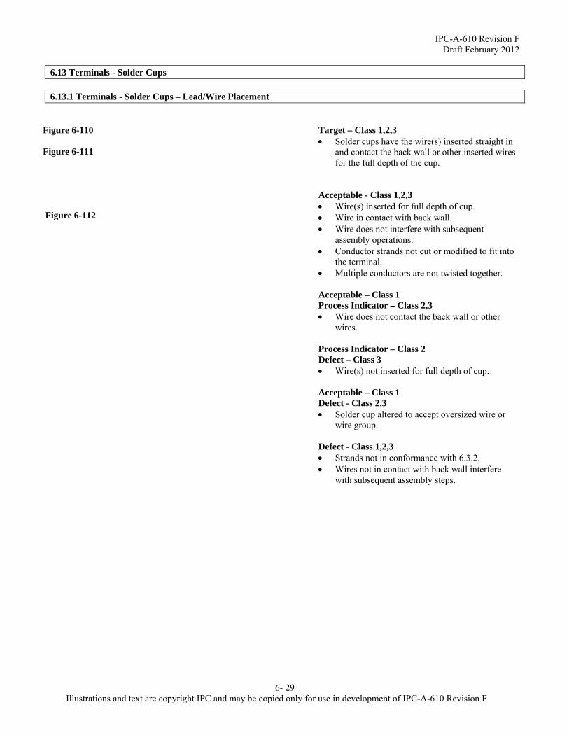
IPC-A-610 Revision F Draft February 2012
6- 29 Illustrations and text are copyright IPC and may be copied only for use in development of IPC-A-610 Revision F
6.13 Terminals - Solder Cups 6.13.1 Terminals - Solder Cups – Lead/Wire Placement
Target – Class 1,2,3 Solder cups have the wire(s) inserted straight in
and contact the back wall or other inserted wires for the full depth of the cup.
Acceptable - Class 1,2,3 Wire(s) inserted for full depth of cup. Wire in contact with back wall. Wire does not interfere with subsequent
assembly operations. Conductor strands not cut or modified to fit into
the terminal. Multiple conductors are not twisted together. Acceptable – Class 1 Process Indicator – Class 2,3 Wire does not contact the back wall or other
wires. Process Indicator – Class 2 Defect – Class 3 Wire(s) not inserted for full depth of cup. Acceptable – Class 1 Defect - Class 2,3 Solder cup altered to accept oversized wire or
wire group. Defect - Class 1,2,3 Strands not in conformance with 6.3.2. Wires not in contact with back wall interfere
with subsequent assembly steps.
Figure 6-110 Figure 6-111
Figure 6-112
IPC-A-610 Revision F Draft February 2012
6- 30 Illustrations and text are copyright IPC and may be copied only for use in development of IPC-A-610 Revision F
6.13.2 Terminals - Solder Cups - Solder These criteria are applicable to either solid or stranded wire, single or multiple wires.
Target – Class 1,2,3 Solder wets the entire inside of the cup. Solder fill is 100%. Acceptable - Class 1,2,3 Thin film of solder on the outside of the cup. Solder fill 75% or more. Solder buildup on the outside of the cup, as long
as it does not affect form, fit or function. Solder visible in or slightly protrudes from the
inspection hole (if one is provided). Defect - Class 1,2,3 Solder vertical fill less than 75%. Solder buildup on outside of the cup negatively
affects form, fit or function. Solder not visible in the inspection hole (if one is
provided). Defect – Class 1,2 Depression of solder between the cup and the
wire is greater than 50% of wire radius. Defect – Class 3 Depression of solder between the cup and the
wire is greater than 25% of wire radius.
Figure 6-113
Figure 6-114 Figure 6-115 Figure 6-116
Figure 6-117
Figure 6-118 Figure 6-119 DELETE THIS FIGURE

IPC-A-610 Revision F Draft February 2012
6- 31 Illustrations and text are copyright IPC and may be copied only for use in development of IPC-A-610 Revision F
6.14 Terminals – AWG 30 and Smaller Diameter Wires 6.14.1 Terminals - AWG 30 and Smaller Diameter Wires – Lead/Wire Placement
Target – Class 1,2,3 Wire has two wraps (720) around terminal post. Wire does not overlap or cross over itself or
other wires terminated on the terminal. Acceptable - Class 1,2,3 Wire has more than one 360° wrap but less than
three. Acceptable – Class 1 Defect - Class 2 Wire has less than 180 wrap. Process Indicator - Class 2 Defect - Class 3 Wire has less than one 360° wrap.
6.15 Terminals –Series Connected These criteria apply when three or more terminals are connected by a common bus wire.
Target – Class 1,2,3 Stress relief radii between each terminal. Turrets - Wire contacts base of terminal or a
previously installed wire, and wraps around or interweaves each terminal.
Hooks - Wire wraps 360 around each terminal. Bifurcated - Wire passes between posts and
contacts base of terminal or previously installed wire.
Pierced/Perforated - Wire contacts two nonadjacent sides of each terminal.
The connection to the first and last terminals meets the required wrap for individual terminals.
Figure 6-120
Figure 6-121
Figure 6-122
Figure 6-123 Figure 6-124 Figure 6-125
IPC-A-610 Revision F Draft February 2012
6- 32 Illustrations and text are copyright IPC and may be copied only for use in development of IPC-A-
610 Revision F
Acceptable - Class 1 Process Indicator - Class 2 Defect - Class 3 Turrets - Wire does not wrap 360 around each
inner terminal or is not interwoven between terminals.
Hooks - Wire wraps less than 360 around inner terminal.
Bifurcated - Wire does not pass between the posts or is not in contact with the terminal base or a previously installed wire.
Pierced/Perforated - Wire does not contact two nonadjacent sides of each inner terminal.
Defect - Class 1,2,3 No stress relief between any two terminals. The connection to the first and last terminals
does not meet the required wrap for individual terminals.
6.16 Terminals - Edge Clip - Position
Target – Class 1,2,3 Clip is centered on land with no side overhang. Acceptable - Class 1,2,3 Clip has 25% maximum overhang off land. Overhang does not reduce spacing below
minimum electrical clearance. Defect - Class 1,2,3 Clip exceeds 25% overhang off land. Clip overhangs land, reducing the spacing below
minimum electrical clearance.
Figure 6-126
Figure 6-127
Figure 6-128

IPC-A-610 Revision F Draft February 2012
7-1 Illustrations and text are copyright IPC and may be copied only for use in licensed translation of IPC-A-610 Revision F.
7 Through Hole Technology This section includes hardware, adhesive, forming, mounting, termination and soldering criteria for through-hole installation. The placement of any component on the electronic assembly does not prevent the insertion or removal of any hardware (tool clearance included) used to mount the assembly. Minimum spacing between installed hardware and the conducting land, component leads or uninsulated components depends on specified voltage and is not less than the specified minimum electrical clearance, see 1.5.3. Bonding material is sufficient to hold the part but does not encapsulate and cover component identification. Visual inspection includes part identification and polarity, assembly sequence, and damage to hardware, component, or board. In addition to the criteria in this section the criteria of Section 5 are applicable. The following topics are addressed in this section: <Chapter Table of Contents will be added at publication> 7.1 Component Mounting 7.1.1 Component Mounting - Orientation This section covers acceptability requirements for the installation, location, and orientation of components and wires mounted onto printed boards. Criteria are given for only the actual mounting or placement of components or wires on electronic assemblies and to standoff spacers. Solder is mentioned where it is an integral part of the placement dimensions, but only as related to those dimensions. Inspection usually starts with a general overall view of the electronic assembly, then follows each component/wire to its connection, concentrating on the lead into the connection, the connection and the tail end of the lead/wire leaving the connection. The wire/lead protrusion step for all lands should be saved for last so that the board can be flipped over and all connections checked together. 7.1.1.1 Component Mounting - Orientation - Horizontal Additional criteria for horizontal mounting of axial leaded components are provided in clauses 7.3.1 (supported holes) and 7.4.1 (unsupported holes).
Target - Class 1,2,3 Components are centered between their lands. Component markings are discernible. Nonpolarized components are oriented so that
markings all read the same way (left-to-right or top-to-bottom).
Figure 7-1

IPC-A-610 Revision F Draft February 2012
7-2 Illustrations and text are copyright IPC and may be copied only for use in licensed translation of IPC-A-610 Revision
F.
Acceptable - Class 1,2,3 Polarized and multilead components are oriented
correctly. When hand formed and hand-inserted, polarization
symbols are discernible. All components are as specified and terminate to
correct lands. Nonpolarized components are not oriented so that
markings all read the same way (left-to-right or top-to-bottom).
Defect - Class 1,2,3 Component is not as specified (wrong part) (A). Component not mounted in correct holes (B). Polarized component mounted backwards (C). Multileaded component not oriented correctly (D).
7.1.1.2 Component Mounting - Orientation - Vertical Additional criteria for vertical mounting of axial leaded components are provided in clauses 7.3.2 (supported holes) and 7.4.2 (unsupported holes). In the examples in Figures 7-4 through 7-6, the arrows printed on the black capacitor casing are pointing to the negative end of the component.
Target - Class 1,2,3 Nonpolarized component markings read from the top
down. Polarized markings are located on top. Acceptable - Class 1,2,3 Polarized part is mounted with a long ground lead. Polarized marking hidden. Nonpolarized component markings read from bottom
to top. Defect – Class 1,2,3 Polarized component is mounted backwards.
Figure 7-2
Figure 7-3 IPC ACTION CHANGE C2 RO R5 TO REFLECT THE WRONT COMPONENT
Figure 7-4
Figure 7-5
Figure 7-6

IPC-A-610 Revision F Draft February 2012
7-3 Illustrations and text are copyright IPC and may be copied only for use in licensed translation of IPC-A-610 Revision F.
7.1.2 Component Mounting - Lead Forming 7.1.2.1 Component Mounting - Lead Forming - Bends
Acceptable – Class 1,2,3 The inside bend radius of component leads meets
requirements of Table 7-1. Table 7-1 Lead Bend Radius
Lead Diameter (D) or Thickness (T)
Minimum Inside Bend Radius (R)
< 0.8 mm [0.031 in] 1 D/T 0.8 mm [0.031 in] to 1.2 mm
[0.0472 in] 1.5 D/T
>1.2 mm [0.0472 in] 2 D/T Note: Rectangular leads use thickness (T). Acceptable – Class 1 Process Indicator – Class2 Defect - Class 3 Inside bend radius does not meet requirements of
Table 7-1. Defect – Class 1,2,3 Lead is kinked. Acceptable – Class 1,2,3 Leads of through-hole mounted component extend at
least 1 lead diameter or thickness but not less than 0.8 mm [0.031 in] from the body, solder bead, or lead weld.
Acceptable - Class 1 Process Indicator - Class 2 Defect - Class 3 Lead bend of through-hole mounted component is
less than 1 lead diameter or 0.8 mm [0.031 in], whichever is less, from the component body, solder bead or component body lead seal.
Defect - Class 1,2,3 Fractured lead weld, solder bead, or component body
lead seal. Lead damage exceeds limits of 7.1.2.3.
Figure 7-7
Figure 7-8
Figure 7-9
Figure 7-10 1. Solder bead 2. Weld
Figure 7-11 Figure 7- 12

IPC-A-610 Revision F Draft February 2012
7-4 Illustrations and text are copyright IPC and may be copied only for use in licensed translation of IPC-A-610 Revision F.
7.1.2.2 Component Mounting - Lead Forming – Stress Relief Components are mounted in any 1 or a combination of the following configurations: In a conventional manner utilizing 90º (nominal) lead bends directly to the mounting hole. With camel hump bends. Configuration incorporating a single camel hump may have the body positioned off-center. Other configurations may be used with agreement of the customer or where design constraints exist. Loop bends may be used if the location of the mounting holes prevents the use of a standard bend and if there is no possibility of shorting the lead to any adjacent component lead or conductor. Use of loop bends may impact circuit impedance, etc., and shall be approved by design engineering. Prepped components with stress bends as shown in Figure 7-14 usually cannot meet the maximum clearance requirements of a straight-legged vertical - radial leaded component, see 7.1.6. Maximum clearance between component and board surface is determined by design limitations and product use environments. The component preparation equipment and manufacturer's suggested component lead bend specifications and capabilities determine limitation. This may require change in tooling to meet requirements for end use.
Acceptable Class 1,2,3 Leads are formed to provide stress relief. Component lead exiting component body is
approximately parallel to major body axis. Component lead entering hole is approximately
perpendicular to board surface. Component centering may be offset as a result of the
type of stress relief bend. Acceptable - Class 1 Process Indicator - Class 2 Defect - Class 3 Lead bends less than 1 lead diameter or thickness but
not less than 0.8 mm [0.031 in] away from body seal. Defect - Class 1,2,3 Damage or fracture of component body-to-lead seal. No stress relief.
Figure 7-13 IPC ACTION TO ASSURE CORRECT PIX WITH FOUR VIEWS IS USED 1. Typically 4 – 8 wire diameters 2. 1 wire diameter minimum 3. 2 wire diameter minimum Figure 7-14
Figure 7-15
Figure 7-16

IPC-A-610 Revision F Draft February 2012
7-5 Illustrations and text are copyright IPC and may be copied only for use in licensed translation of IPC-A-610 Revision F.
7.1.2.3 Component Mounting - Lead Forming - Damage These criteria are applicable whether leads are formed manually or by machine or die.
Acceptable - Class 1,2,3 No nicks or deformation exceeding 10% of the
diameter, width or thickness of the lead. See 5.2.1 for exposed basis metal criteria.
Defect - Class 1,2,3 Lead is damaged more than 10% of the lead diameter
or thickness. Lead deformed from repeated or careless bending. Defect - Class 1,2,3 Heavy indentations such as serrated pliers mark. Lead diameter is reduced more than 10%.
7.1.3 Component Mounting - Leads Crossing Conductors
Acceptable - Class 1,2,3 Sleeve does not interfere with formation of the
required solder connection (A). Sleeve covers area of protection designated (B). Defect - Class 2,3 Splitting and/or unraveling of sleeving (A). Defect - Class 1,2,3 Component leads and wires required to have sleeving
are not sleeved. Damaged/insufficient sleeving does not provide
protection from shorting. Sleeving interferes with formation of the required
solder connection. A component lead crossing an electrically
noncommon conductor violates minimum electrical clearance (B).
Figure 7-17
Figure 7-18
Figure 7-19
Figure 7-20
Figure 7-21

IPC-A-610 Revision F Draft February 2012
7-6 Illustrations and text are copyright IPC and may be copied only for use in licensed translation of IPC-A-610 Revision F.
7.1.4 Component Mounting - Hole Obstruction
Acceptable - Class 1,2,3 Parts and components are mounted such that they do
not obstruct solder flow onto the primary side (solder destination side) lands of plated-through holes required to be soldered.
Process Indicator - Class 2 Defect - Class 3 Parts and components obstruct solder flow onto the
primary side (solder destination side) lands of plated-through holes required to be soldered.
Defect Class 1,2,3 Parts and components are mounted such that they
violate minimum electrical clearance.
7.1.5 Component Mounting – DIP/SIP Devices and Sockets These criteria are applicable to Dual-in-Line Packages (DIP), Single-in-Line Packages (SIP) and sockets. Note: In some cases a heat sink may be located between the component and the printed board; in these cases other criteria may be specified.
Target - Class 1,2,3 Standoff step on all leads rests on the land. Lead protrusion meets requirements, see 7.3.3 and
7.4.3. Acceptable - Class 1,2,3 Amount of tilt is limited by minimum lead protrusion
and height requirements. Defect - Class 1,2,3 Tilt of the component exceeds maximum component
height limits. Lead protrusion does not meet acceptance
requirements due to tilt of component.
Figure 7-22 1. Insulating washer 2. Spacer
Figure 7-23 1. Hard mount 2. Air 3. Component body 4. Solder
Figure 7-24 1. Nonmetal 2. Mounting hardware 3. Component case 4. Conductive pattern
Figure 7-25 Figure 7-26
Figure 7-27 Figure 7-28 Figure 7-29
Figure 7-30 Figure 7-31 Figure 7-32

IPC-A-610 Revision F Draft February 2012
7-7 Illustrations and text are copyright IPC and may be copied only for use in licensed translation of IPC-A-610 Revision F.
7.1.6 Component Mounting - Radial Leads – Vertical
Target - Class 1,2,3 Component is perpendicular and base is parallel to
board. Clearance between base of component and board
surface/land is between 0.3 mm [0.012 in] and 2 mm [0.079 in].
Acceptable - Class 1,2,3 Component tilt does not violate minimum electrical
clearance (C). Process Indicator - Class 2,3 Space between component base and board
surface/land is less than 0.3 mm [0.012 in] or more than 2 mm [0.079 in], see 7.1.4.
Defect - Class 1,2,3 Violates minimum electrical clearance. Note: Some components cannot be tilted due to mating requirements with enclosures or panels, for example toggle switches, potentiometers, LCDs, and LEDs.
7.1.6.1 Component Mounting - Radial Leads – Vertical - Spacers Spacers used for mechanical support or to compensate for component weight need to be in full contact with both component and board surface.
Target - Class 1,2,3 Spacer is in full contact with both component and
board. Lead is properly formed. Acceptable (Supported Holes) - Class 1,2 Process Indicator (Supported Holes) - Class 3 Defect (Unsupported Holes) - Class 1,2,3 Spacer is not in full contact with component and
board. Edges of spacer contact both component and board.
Figure 7-33
Figure 7-34
Figure 7-35 1. Spacer 2. Contact Figure 7-36
Figure 7-37

IPC-A-610 Revision F Draft February 2012
7-8 Illustrations and text are copyright IPC and may be copied only for use in licensed translation of IPC-A-610 Revision
F.
Acceptable (Supported Holes) - Class 1 Process Indicator (Supported Holes) - Class 2 Defect (Supported Holes) - Class 3 Defect (Unsupported Holes) – Class 1,2,3 Spacer is not in contact with component and board;
Figures 7-38 (A), 7-39. Lead is improperly formed; Figure 7-38 (B). Defect - Class 2,3 Spacer is inverted; Figure 7-38 (C).
7.1.7 Component Mounting - Radial Leads - Horizontal
Target - Class 1,2,3 The component body is in flat contact with the
board's surface. Bonding material is present, if required. See 7.2.2. Acceptable - Class 1,2,3 Component in contact with board on at least 1 side
and/or surface. Note: When documented on an approved assembly drawing, a component may be either side mounted or end mounted. The body may need to be bonded or otherwise secured to the board to prevent damage when vibration and shock forces are applied. Defect - Class 1,2,3 Unbonded component body not in contact with
mounting surface. Bonding material not present if required.
7.1.8 Component Mounting - Connectors These criteria apply to soldered connectors. For connector pin criteria see 4.3. For connector damage criteria see 9.5. Connector module/pin misalignment, defined in this section, is to be measured at the connector lead-in area/hole (for receptacles) or at the pin tip (for pin headers). In cases where an assembly connector is composed of two or more identical connector modules, modules manufactured by different suppliers shall not be mixed.
Figure 7-38
Figure 7-39
Figure 7-40
Figure 7-41
Figure 7-42

IPC-A-610 Revision F Draft February 2012
7-9 Illustrations and text are copyright IPC and may be copied
only for use in licensed translation of IPC-A-610 Revision F.
Target - Class 1,2,3 Connector is flush with board. Lead protrusion meets requirements. Board lock (if equipped) is fully inserted/snapped into the
board. Acceptable - Class 1,2,3 Board lock is fully inserted/snapped through the board. Any tilt or misalignment, provided:
Minimum lead protrusion is met. Maximum height requirements are not exceeded. Mates correctly.
Defect - Class 1,2,3 Will not mate when used in application due to angle or
misalignment. Component violates height requirements. Board lock is not fully inserted/snapped into board. Lead protrusion does not meet acceptance requirements. Note: A trial mating of connector to connector or to assembly may be required to assure the connectors meet form, fit and function requirement.
7.1.8.1 Right Angle These criteria are applicable to right angle soldered connectors with pin spacing ≥ 2.5 mm [0.098 in].
Target - Class 1,2,3 Connector is mounted flush with the surface of the board
(A). All modules of a multi-part connector are aligned and are
mounted flush to adjoining modules (B). Acceptable – Class 1 Connector spacing does not affect mating of connector
with assembling requirements e.g., face plates, bracket, mating connector, etc.
Acceptable – Class 2,3 Connector-to-board spacing is equal to or less than 0.13
mm [0.005 in] (not shown). Maximum misalignment is less than 0.25 mm [0.010 in]
across the contact openings of all connectors in the connector lineup, Figure 7-50.
Figure 7-43 Figure 7-44
Figure 7-45 Figure 7-46
Figure 7-47
Figure 7-48 Figure7-49
Figure 7-50

IPC-A-610 Revision F Draft February 2012
7-10 Illustrations and text are copyright IPC and may be copied
only for use in licensed translation of IPC-A-610 Revision F.
Defect – Class 1 Connector spacing affects mating of connector with
assembling requirements e.g., face plates, bracket, mating connector, etc.
Defect – Class 2,3 Connector-to-board spacing is greater than 0.13 mm
[0.005 in] (not shown). Maximum misalignment is greater than 0.25 mm [0.010
in] across the faces (contact openings) of all modules (connectors) in the connector lineup.
7.1.8.2 Vertical Shrouded Pin Headers and Vertical Receptacle Connectors These criteria are applicable to vertical shrouded pin headers and vertical receptacle connectors that are 2 mm – 2.54 mm [0.08 – 0.1 in] pin spacing.
Target - Class 1,2,3 Connector is mounted flush with the surface of the
board. All modules of a multi-part connector are aligned and
are mounted flush to adjoining modules (not shown). Acceptable – Class 1, Connector spacing does not affect mating of
connector with assembling requirements e.g., face plates, bracket, mating connector, etc.
Acceptable – Class 2,3 Connector-to-board spacing is equal to or less than
0.13 mm [0.005 in] (not shown). Individual connector/modules contact openings,
requiring alignment, are equal to, or less than, 0.25 mm [0.010 in], with adjacent modules (not shown).
Maximum misalignment between any two modules/pins in the connector lineup is less than 0.25 mm [0.010 in] (not shown).
Defect – Class 1 Connector spacing affects mating of connector with
assembling requirements e.g., face plates, bracket, mating connector, etc.
Defect – Class 2,3 Connector-to-board spacing is greater than 0.13 mm
[0.005 in]. Maximum misalignment between any two
modules/pins in the connector lineup is greater than 0.25 mm [0.010 in] (not shown).
Figure 7-51
Figure 7-52
Figure 7-53
IPC-A-610 Revision F Draft February 2012
7-11 Illustrations and text are copyright IPC and may be copied only for use in licensed translation of IPC-A-610 Revision F.
7.1.9 Component Mounting - High Power
Acceptable - Class 1,2,3 Hardware in proper sequence. Leads on components attached by fastening devices
are not clinched (not shown). Insulating washer provides electrical isolation when
required. Thermal compound, if used, does not interfere with
formation of required solder connections. Note: Where a thermal conductor is specified, it is placed between mating surfaces of the power device and the heat sink. Thermal conductors may consist of a thermally conductive washer or of an insulating washer with a thermally conductive compound. Defect - Class 1,2,3 Improper hardware sequence. Sharp edge of washer is against insulator. Hardware is not secure. Thermal compound, if used, does not permit
formation of required solder connections.
7.1.10 Component Mounting – Conductive Cases Where a potential for shorting (violation of minimum electrical clearance) exists between conductive component bodies, at least 1 of the bodies shall be protected by an insulator. 7.2 Component Securing 7.2.1 Component Securing - Mounting Clips
Target - Class 1,2,3 Uninsulated metallic component insulated from
underlying circuitry with insulating material. Uninsulated metallic clips and holding devices used
to secure components insulated from underlying circuitry with insulating material.
Spacing between land and Uninsulated component body exceeds minimum electrical clearance. <Sep2011>
Figure 7-54 1. Metal 2. Terminal lug 3. Component case 4. Nut 5. Lock washer 6. Screw 7. Nonmetal Figure 7-55 1. High power component 2. Insulating washer (when required) 3. Heat sink (may be metal or nonmetal) 4. Terminal lug 5. Lock washer 6. Insulator sleeve
Figure 7-56 1. Lock washer between terminal lug and component case. Figure 7-57 1. Sharp edge of washer against insulator 2. Terminal lug 3. Metal heat sink
Figure 7-58 1. Conductive patterns 2. Metallic mounting clip 3. Insulation material 4. Clearance

IPC-A-610 Revision F Draft February 2012
7-12 Illustrations and text are copyright IPC and may be copied only for use in licensed translation of IPC-A-610 Revision
F.
Acceptable - Class 1,2,3 The clip makes contact to both sides of the
component (A). The component is mounted with the center of gravity
within the confines of the clip (B,C). The end of the component is flush with or extends
beyond the end of the clip (C). Defect - Class 1,2,3 Spacing between land and uninsulated component
body is less than minimum electrical clearance, Figure 7-60.
Uninsulated metallic clip or holding device is not insulated from underlying circuitry.
Clip does not restrain component, Figure 7-61 (A) Component center or center of gravity not within the
confines of the clip, Figure 7-61 (B, C.
7.2.2 Component Securing - Adhesive Bonding The criteria below shall be used when staking is required and criteria are not provided on the drawing. These criteria do not apply to SMT components (see 8.1). Visual inspection of staking may be performed without magnification. Magnification from 1.75X to 4X may be used for referee purposes. Refer to adhesive manufacturer’s guidelines for curing requirements.
Figure 7-59 1. Clip 2. Nonsymmetrical body 3. Top view 4. Center of gravity
Figure 7-60 Figure 7-61

IPC-A-610 Revision F Draft February 2012
7-13 Illustrations and text are copyright IPC and may be copied only for use in licensed translation of IPC-A-610 Revision F.
7.2.2.1 Component Securing - Adhesive Bonding -Non-Elevated Components
Acceptable - Class 1,2,3 On an unsleeved horizontally mounted component
the staking material adheres to component for at least 50% of its length (L), and 25% of its diameter (D), on 1 side. The build up of staking material does not exceed 50% of the component diameter. Adhesion to the mounting surface is evident. The staking material is approximately centered on the body.
On an unsleeved vertically mounted component there are a minimum of two beads of staking material for at least 25% of its length (L), and 25% of its circumference. Adhesion to the mounting surface is evident.
Sleeved axial leaded components (except glass bodied components) have staking material in contact with both end faces of the component for 25% to 50% of the component diameter (height).
Glass bodied components are sleeved, when required, prior to staking material attachment.
Adhesives, e.g., staking, bonding, do not contact an unsleeved area of a sleeved glass body component.
Sleeved glass bodied components have staking material applied to both sides of the component from 50% to 100% of the component length for a minimum of 25% of component height.
On multiple vertically mounted components the staking material adheres to each component for at least 50% of its length (L), and the adhesion is continuous between components. Adhesion to the mounting surface is evident. The staking material also adheres to each component for a minimum 25% of its circumference.
Adhesive is cured. Not Established - Class 1 Process Indicator - Class 2 Defect – Class 3 Staking material in excess of 50% diameter of
unsleeved horizontally mounted components provided the top of the component is visible for the entire length of the component body.
Sleeved glass bodied components do not have staking material applied to both sides of the component from 50% to 100% of the component length.
Figure 7-62 1. Adhesive 2. Top view 3. 25% Circumference Figure 7-63 1. Top view 2. Adhesive
Figure 7-64 1. <50% length (L) 2. Top view 3. < 25% circumference Figure 7-65

IPC-A-610 Revision F Draft February 2012
7-14 Illustrations and text are copyright IPC and may be copied only for use in licensed translation of IPC-A-610 Revision
F.
Process Indicator – Class 1 Defect – Class 2,3 Sleeved axial leaded components (except glass
bodied components) do not have staking material in contact with both end faces of the component or the adhesive is less than 25% or greater than 50% of the component diameter (height).
The top of the component body is not visible for the entire length because of staking material coverage.
Sleeved glass bodied components do not have staking material for a minimum of 25% of component height.
Sleeved glass bodied components do not have staking material applied to both sides of the component from 50% to 100% of the component length.
Not Established - Class 1 Defect – Class 2,3 The top of sleeved glass bodied components is not
visible the entire length of the component body. Defect - Class 1,2,3 On an unsleeved horizontally mounted component the
staking material adheres to component less than 50% of its length (L) or less than 25% of its diameter (D), on 1 side.
On an unsleeved vertically mounted component there are less than two beads of staking material adhering to the component less than 25% of its length (L) or less than 25% of its circumference.
Staking material in excess of 50% diameter of horizontally mounted components and the top of the component is not visible for the entire length of the component body.
On multiple vertically mounted components the staking material adheres to each component for less than 50% of its length (L), for less than 25% of its circumference, and the adhesion is not continuous between components.
Adhesion to the mounting surface is not evident. Uninsulated metallic case components bonded over
conductive patterns. Staking material on areas to be soldered preventing
compliance to Tables 7-4, 7-5 or 7-7. Rigid adhesives, e.g., staking, bonding, contact an
unsleeved area of a sleeved glass body component, Figure 7-65.
Staking material is not cured.
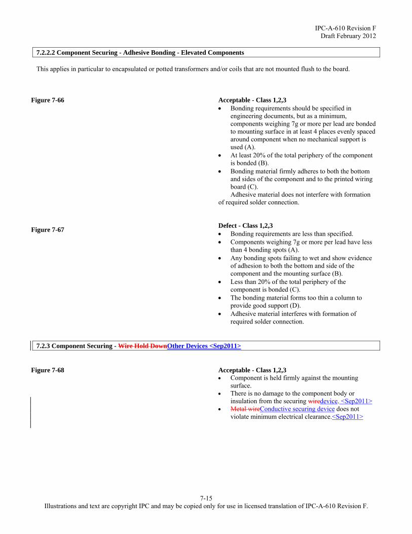
IPC-A-610 Revision F Draft February 2012
7-15 Illustrations and text are copyright IPC and may be copied only for use in licensed translation of IPC-A-610 Revision F.
7.2.2.2 Component Securing - Adhesive Bonding - Elevated Components This applies in particular to encapsulated or potted transformers and/or coils that are not mounted flush to the board.
Acceptable - Class 1,2,3 Bonding requirements should be specified in
engineering documents, but as a minimum, components weighing 7g or more per lead are bonded to mounting surface in at least 4 places evenly spaced around component when no mechanical support is used (A).
At least 20% of the total periphery of the component is bonded (B).
Bonding material firmly adheres to both the bottom and sides of the component and to the printed wiring board (C).
Adhesive material does not interfere with formation of required solder connection. Defect - Class 1,2,3 Bonding requirements are less than specified. Components weighing 7g or more per lead have less
than 4 bonding spots (A). Any bonding spots failing to wet and show evidence
of adhesion to both the bottom and side of the component and the mounting surface (B).
Less than 20% of the total periphery of the component is bonded (C).
The bonding material forms too thin a column to provide good support (D).
Adhesive material interferes with formation of required solder connection.
7.2.3 Component Securing - Wire Hold DownOther Devices <Sep2011>
Acceptable - Class 1,2,3 Component is held firmly against the mounting
surface. There is no damage to the component body or
insulation from the securing wiredevice. <Sep2011> Metal wireConductive securing device does not
violate minimum electrical clearance.<Sep2011>
Figure 7-66
Figure 7-67
Figure 7-68
IPC-A-610 Revision F Draft February 2012
7-16 Illustrations and text are copyright IPC and may be copied only for use in licensed translation of IPC-A-610 Revision F.
7.3 Supported Holes 7.3.1 Supported Holes – Axial Leaded – Horizontal
Target - Class 1,2,3 The entire body length of the component is in contact
with the board surface. Components required to be mounted off the board are
at least 1.5 mm [0.059 in] from the board surface; e.g., high heat dissipating.
Acceptable - Class 1,2 The maximum clearance (C) between the component
and the board surface does not violate the requirements for lead protrusion (see 7.3.3) or component height (H). (H) is a user-determined dimension.
Acceptable - Class 3 Clearance (C) between the component body and the
board does not exceed 0.7 mm [0.028 in]. Process Indicator - Class 3 The farthest distance (D) between the component
body and the board is larger than 0.7 mm [0.028 in]. Defect – Class 3 The distance (D) between the component body and
the board is larger than 1.5 mm [0.059 in]. Defect - Class 1,2,3 Component height exceeds user-determined
dimension (H). Components required to be mounted above the board
surface are less than 1.5 mm [0.059 in] (C) from the board surface.
Figure 7-69 Figure 7-70
Figure 7-71
IPC-A-610 Revision F Draft February 2012
7-17 Illustrations and text are copyright IPC and may be copied only for use in licensed translation of IPC-A-610 Revision F.
7.3.2 Supported Holes – Axial Leaded – Vertical
Target - Class 1,2,3 The clearance (C) of the component body or weld
bead above the land is 1 mm [0.039 in]. The component body is perpendicular to the board. The overall height does not exceed maximum design
height requirements (H). Acceptable - Class 1,2,3 The component or weld bead clearance (C) above the
land meets the requirements of Table 7-2. The angle of the component lead does not cause a
violation of minimum electrical clearance. Table 7-2 Component to Land Clearance
Class 1 Class 2 Class 3 C (min) 0.1mm
[0.0039 in] 0.4 mm
[0.016 in] 0.8 mm
(0.031 in) C (max) 6 mm
[0.24 in] 3 mm
[0.12 in] 1.5 mm
[0.059 in]
7.3.2 Supported Holes – Axial Leaded – Vertical (cont.)
Acceptable - Class 1 Process Indicator - Class 2,3 The component or weld bead clearance (C) is greater
than the maximum given in Table 7-2 The component or weld bead clearance (C) is less
than the minimum given in Table 7-2. Defect - Class 1,2,3 Components violate minimum electrical clearance. Component height does not meet form, fit or
function. Component height (H) exceeds user-determined
dimension.
Figure 7-72
Figure 7-73
Figure 7-74 IPC ACTION MODIFY TOP BEND IN MIDDLE VIEW TO MATCH OTHER TWO COMPONENTS

IPC-A-610 Revision F Draft February 2012
7-18 Illustrations and text are copyright IPC and may be copied only for use in licensed translation of IPC-A-610 Revision F.
7.3.3 Supported Holes –Wire/Lead Protrusion Lead protrusion (Table 7-3) should shall not allow a possibility of violating minimum electrical spacing, damage to soldered connections due to lead deflection, or penetration of static protective packaging during subsequent handling. Note: High frequency applications may require more precise control of lead extensions to prevent violation of functional design considerations. Table 7-3 Protrusion of Wires/Leads in Supported Holes
Class 1 Class 2 Class 3 (L) min. End is discernible in the solder.1 (L) max.2 No danger of shorts 2.5 mm [0.0984 in] 1.5 mm [0.0591 in]
Note 1. For components having manufacturer’s pre-established lead lengths that are less than board thickness, and the components or lead shoulders are flush to the board surface, the lead end is not required to be visible in the subsequent solder connection, see 1.4.1.5. Note 2: Connector leads, relay leads, tempered leads and leads greater than 1.3 mm (.050) diameter are exempt from the maximum length requirement provided that they do not violate minimum electrical spacing.
Acceptable – Class 1,2,3 The leads protrude beyond the land within the
specified minimum and maximum (L) of Table 7-3, provided there is no danger of violating minimum electrical clearance.
The leads meet the design length (L) requirements when specified.
Defect - Class 1,2,3 Lead protrusion does not meet the requirements of
Table 7-3. Lead protrusion violates minimum electrical
clearance. Lead protrusion exceeds maximum design height
requirements.
7.3.4 Supported Holes – Wire/Lead Clinches Component leads in through-hole connections may be terminated using a straight through, partially clinched or clinched configuration. The clinch should be sufficient to provide mechanical restraint during the soldering process. The orientation of the clinch relative to any conductor is optional. DIP leads should have at least two diagonally opposing leads partially bent outward. Leads greater than 1.3 mm (.050 inch) thick or diameter should not be bent nor formed for mounting purposes. Tempered leads shall not be terminated with a full clinched configuration. <Sep2011>. The lead meets the protrusion requirements of Table 7-3 when measured vertically from the land surface and does not violate minimum electrical clearance requirements. This section applies to terminations with a clinching requirement. Other requirements may be specified on relevant specifications or drawings. Partially clinched leads for part retention are considered as unclenched leads and shall meet protrusion requirements.
Figure 7-75 Figure 7-76
Figure 7-77
IPC-A-610 Revision F Draft February 2012
7-19 Illustrations and text are copyright IPC and may be copied only for use in licensed translation of IPC-A-610 Revision
F.
Target - Class 1,2,3 Lead end is parallel to the board and direction of the
clinch is along the connecting conductor. Acceptable - Class 1,2,3 The clinched lead does not violate the minimum
electrical clearance (C) between noncommon conductors.
The protrusion (L) beyond the land is not greater than the similar length allowed for straight-through leads. See Figure 7-79 and Table 7-3.
Defect - Class 1,2,3 The lead is clinched toward an electrically
noncommon conductor and violates minimum electrical clearance (C).
7.3.5 Supported Holes – Solder Criteria for soldered supported holes are provided in 7.3.5.1 through 7.3.5.12. These criteria are applicable regardless of the soldering process, e.g., hand soldering, wave soldering, intrusive soldering, etc.
Target - Class 1,2,3 No void areas or surface imperfections. Lead and land are well wetted. Lead is discernible. 100% solder fillet around lead. Solder covers lead and feathers out to a thin edge on
land/conductor. No evidence of fillet lifting, see 5.2.11.<Sep2011> Acceptable - Class 1,2,3 Lead is discernible in the solder. Acceptable - Class 1 Process Indicator - Class 2,3 Fillet convex, and as an exception to Table 7-4, lead
not discernible due to excess solder, providing visual evidence of the lead in the hole can be determined on the primary side.
Fillet is lifted from land on primary side but there is no land damage (not shown) see 10.8.2.<Sep2011>
Figure 7-78
Figure 7-79
Figure 7-80 1. Noncommon conductor Figure 7-81
Figure 7-82 1. Land area
Figure 7-83 Figure 7-84
Figure 7-85 Figure 7-86

IPC-A-610 Revision F Draft February 2012
7-20 Illustrations and text are copyright IPC and may be copied only for use in licensed translation of IPC-A-610 Revision
F.
Defect - Class 1,2,3 Lead not discernible due to bent lead. Solder not wetted to lead or land. Solder coverage does not comply with Table 7-4.
Table 7-4 Plated-Through Holes with Component Leads - Minimum Acceptable Solder Conditions1
Criteria Class 1 Class 2 Class 3 A. Vertical fill of solder2,3 (see7.3.5.1) Not Specified 75% 75% B. Circumferential wetting of lead and barrel on solder destination side (see 7.3.5.2).
Not Specified 180 270
C. Percentage of original land area covered with wetted solder on solder destination side (see 7.3.5.3).
0%
D. Circumferential wetting of lead and barrel on solder source side (see 7.3.5.4). 270 270 330
E. Percentage of land area covered with wetted solder on solder source side (see 7.3.5.5).
75% 75% 75%
Note 1. Wetted solder refers to solder applied by the solder process. For intrusive soldering there may not be an external fillet between the lead and the land. Note 2. The 25% unfilled height includes both source and destination side depressions. Note 3. Class 2 may have less than 75% vertical hole fill as noted in 7.3.5.1. Defect - Class 1,2,3 Solder connections are not in compliance with Table 7-4. 7.3.5.1 Supported Holes – Solder - Vertical fill (A)
Target - Class 1,2,3 There is 100% fill. Acceptable - Class 1,2,3 Minimum 75% fill. A maximum of 25% total
depression, including both secondary and primary sides is permitted.
Defect - Class 2,3 Vertical fill of hole is less than 75%.
Figure 7-87
Figure 7-88
Figure 7-89
Figure 7-90 1. Vertical fill meets requirements of Table 7-4 2. Solder destination side 3. Solder source side

IPC-A-610 Revision F Draft February 2012
7-21 Illustrations and text are copyright IPC and may be copied only for use in licensed translation of IPC-A-610 Revision
F.
Not Specified - Class 1 Acceptable - Class 2 Defect - Class 3 As an exception to the fill requirements of Table 7-4,
the minimum permissible vertical fill of a PTH is 50% or 1.19mm (0.047 inch), whichever is less, for Class 2 products provided the following conditions are met: The PTH is connected to thermal or conductor
layers that act as thermal heat sinks. The component lead is discernible in the Side B
solder connection of Figure 7-91. The solder fillet on Side B of Figure 7-91 has
wetted 360 of the PTH barrel wall and 360 of the lead.
Surrounding PTHs meet requirements of Table 7-4.
Note: Less than 100% solder fill may not be acceptable in some applications, e.g., thermal shock, electrical performance. The user is responsible for identifying these situations to the manufacturer.
7.3.5.2 Supported Holes – Solder – Primary Side - Lead to Barrel (B)
Target – Class 1,2,3 360º wetting present on lead and barrel. Not Specified - Class 1 Acceptable - Class 2 Minimum 180 wetting present on lead and barrel,
Figure 7-93. Acceptable - Class 3 Minimum 270 wetting present on lead and barrel,
Figure 7-94.
7.3.5.2 Supported Holes – Solder – Solder Destination Primary Side - Lead to Barrel (B) (cont.);
Defect - Class 2 Less than 180 wetting on lead or barrel. Defect - Class 3 Less than 270 wetting on lead or barrel.
Figure 7-91
Figure 7-92
Figure 7-93 Figure 7-94
Figure 7-95 Figure 7-96

IPC-A-610 Revision F Draft February 2012
7-22 Illustrations and text are copyright IPC and may be copied only for use in licensed translation of IPC-A-610 Revision F.
7.3.5.3 Supported Holes – Solder - Solder Destination Primary Side - Land Area Coverage (C)
Acceptable - Class 1,2,3 The land area does not need to be wetted with solder
on the primary solder destination side.
7.3.5.4 Supported Holes – Solder - Solder Source Secondary Side - Lead to Barrel (D)
Acceptable - Class 1,2 Minimum 270 fillet and wetting (lead, barrel and
termination area). Acceptable - Class 3 Minimum 330 fillet and wetting (lead, barrel and
termination area). (Not Shown.) Defect – Class 1,2,3 Does not meet requirements of Table 7-4.
7.3.5.5 Supported Holes – Solder - Secondary Solder Source Side - Land Area Coverage (E)
Target – Class 1,2,3 Land area completely covered on the secondary
solder source side. Acceptable - Class 1,2,3 Minimum 75% of land area covered with wetted
solder on the secondary solder source side. Defect – Class 1,2,3 Does not meet requirements of Table 7-4.
7.3.5.6 Supported Holes – Solder Conditions - Solder in Lead Bend
Acceptable - Class 1,2,3 Solder in lead bend area does not contact the
component body. There is no defect provided all other mounting and fillet criteria are acceptable; also see 7.3.5.7.
Figure 7-97
Figure 7-98
Figure 7-99
Figure 7-100 Figure 7-101
Figure 7-102
Figure 7-103 Figure 7-104

IPC-A-610 Revision F Draft February 2012
7-23 Illustrations and text are copyright IPC and may be copied only for use in licensed translation of IPC-A-610 Revision F.
7.3.5.7 Supported Holes – Solder Conditions – Touching Through-Hole Component Body
Acceptable – Class 1,2,3 Solder does not touch the component body or end
seal. Defect - Class 1,2,3 Solder contacts the component body or end seal.
Exception see 7.3.5.8.
7.3.5.8 Supported Holes – Solder Conditions - Meniscus in Solder
Target - Class 1,2,3 There is 1.2mm (0.048 in) separation between the
coating meniscus and the solder fillet. Acceptable Class 1 Components with a coating meniscus can be mounted
with the meniscus into the solder provided: 360º wetting on the secondary side. Lead coating meniscus is not discernible within
the connection on the secondary side. Acceptable Class 2,3 Coating meniscus is not in the plated through hole
and there is discernible clearance between the meniscus and the solder fillet.
Process Indicator - Class 2 Coating meniscus is in the plated through hole but
solder joint meets the requirements of Table 7-4. Defect - Class 3 Coating meniscus is in the plated through hole. Coating meniscus is embedded in the solder
connection. Defect - Class 1,2,3 Does not exhibit good wetting on secondary side. Does not meet requirements of Table 7-4. Note: When required for certain applications, meniscus on the components are to be controlled to ensure that, with components fully seated, the meniscus on the leads does not enter the plated-through holes of the assembly. (Example: high frequency applications, very thin PCBs.)
Figure 7-105
Figure 7-106 Figure 7-107
Figure 7-108
Figure 7-109 1. Class 1 2. Class 2,3
Figure 7-110
IPC-A-610 Revision F Draft February 2012
7-24 Illustrations and text are copyright IPC and may be copied only for use in licensed translation of IPC-A-610 Revision F.
7.3.5.9 Lead Cutting after Soldering The following criteria apply to printed board assemblies where the connections have been trimmed after soldering. Leads may be trimmed after soldering provided the cutters do not damage the component or solder connection due to physical shock. For Classes 2 and 3, when lead cutting is performed after soldering, the solder terminations shall be visually inspected at 10X to ensure that the original solder connection has not been damaged, i.e., fractured or deformed. As an alternative to visual inspection, the solder connections may be reflowed. If the solder connection is reflowed this is considered part of the soldering process and is not to be considered rework. This requirement is not intended to apply to components that are designed such that a portion of the lead is intended to be removed after soldering, i.e., break away tie bars).
Acceptable - Class 1,2,3 No fractures between lead and solder. Lead protrusion within specification, see 7.3.3. Defect - Class 1,2,3 Evidence of fracture between lead and solder fillet. Defect – Class 3 Lead trimming that cuts into the solder fillet and is
not reflowed.
7.3.5.10 Supported Holes – Coated Wire Insulation in Solder These requirements apply when the solder connection meets the minimum requirements of Table 7-4. See 6.2.3 for extruded insulation clearance requirements. This section applies to coatings that may extend into the connection during soldering operations, provided the material is not corrosive.
Target - Class 1,2,3 Clearance of 1 wire diameter between solder fillet
and insulation. Acceptable - Class 1,2,3 Coating is entering solder connection on primary side
and meets minimum requirements of Table 7-4. Defect - Class 1,2,3 Solder connection exhibits poor wetting and does not
meet the minimum requirements of Table 7-4. Coating is discernible on secondary side.
Figure 7-111 1. Lead protrusion
Figure 7-112
Figure 7-113
Figure 7-114
Figure 7-115

IPC-A-610 Revision F Draft February 2012
7-25 Illustrations and text are copyright IPC and may be copied only for use in licensed translation of IPC-A-610 Revision F.
7.3.5.11 Supported Holes – Interfacial Connection without Lead - Vias Supported holes used for interfacial connection not exposed to solder because of permanent or temporary masks need not be filled with solder. Supported holes or vias without leads, after exposure to wave, dip or drag soldering equipment are to meet these acceptability requirements.
Target - Class 1,2,3 Holes are completely filled with solder. The tops of lands show good wetting. Acceptable - Class 1,2,3 Sides of holes are wetted with solder. Acceptable - Class 1 Process Indicator - Class 2,3 Solder has not wetted side of holes. Note: There is no defect condition for this. Note: Solder capped PTHs have the possibility of entrapping contaminants that are difficult to remove if cleaning is required.
7.3.5.12 Supported Holes – Board in Board No board in board criteria have been established for Class 3 assemblies. From IPC-T-50: “Daughter Board - A printed board that is fastened to a mother board and electrically connected.” When required, attachment will include additional mechanical support aids, e.g., adhesives or hardware, to ensure the connections will not be damaged in the intended service environment. Table 7-5 Board in Board - Minimum Acceptable Solder Conditions1
Criteria Class 1 Class 2
Vertical fill of solder2 75% 75%
Wetting on primary side (solder destination side) daughter board land to PCA solder connection width
50% 75%
Percentage of land area on PCA (mother board) covered with wetted solder on primary side (solder destination side)
0%
Fillet and wetting solder connection width on secondary side (solder source side) of PCA (mother board) to lands on both sides of daughter board.
50% 75%
Percentage of land area on PCA (mother board) covered with wetted solder on secondary side (solder source side)
75% 75%
Note 1. Wetted solder refers to solder applied by the solder process. Note 2. The 25% unfilled height includes both source and destination side depressions.
Figure 7-116
Figure 7-117
Figure 7-118

IPC-A-610 Revision F Draft February 2012
7-26 Illustrations and text are copyright IPC and may be
copied only for use in licensed translation of IPC-A-610 Revision F.
Acceptable – Class 1,2 Daughter board is mounted perpendicular to
PCA. Daughter board is flush to PCA. Mechanical constraints, if required, are properly
attached. Vertical fill of solder is 75%.
7.3.5.12 Supported Holes – Board in Board (cont.)
Acceptable – Class 1 Solder is wetted a minimum of 50% width (X) of
each of the sides of the daughter board lands (L) to PCA on secondary side (solder source side).
Solder is wetted a minimum of 50% width (X) of each of the sides of the daughter board land (L) to PCA on primary side (solder destination side).
Acceptable – Class 2 Solder is wetted a minimum of 75% width (X) of
each of the sides of the daughter board land (L) to PCA on secondary side (solder source side).
Solder is wetted a minimum of 75% width (X) of each of the sides of the daughter board land (L) to PCA on primary side (solder destination side).
7.3.5.12 Supported Holes – Board in Board (cont.)
Defect – Class 1,2 Daughter board angle stresses mounting through-
hole tabs. Required mechanical constraints not present or
not properly attached. Vertical fill of solder is less than 75%. Solder not wetted to each of the sides of daughter
board lands or PCA land. Defect – Class 1 Solder is wetted less than 50% width (X) of both
sides of the daughter board land (L) to PCA on secondary side (solder source side).
Solder is wetted less than 50% width (X) of each of the sides of the daughter board land (L) to PCA on primary side (solder destination side).
Figure 7-119 Figure 7-120
Figure 7-121
Figure 7-122 Figure 7-123
Figure 7-124 Figure 7-125
IPC-A-610 Revision F Draft February 2012
7-27 Illustrations and text are copyright IPC and may be
copied only for use in licensed translation of IPC-A-610 Revision F.
Defect – Class 2 Solder is wetted less than 75% width (X) of each
of the sides of the daughter board land (L) to PCA on secondary side (solder source side).
Solder is wetted less than 75% width (X) of each of the sides of the daughter board land (L) to PCA on primary side (solder destination side).
7.4 Unsupported Holes 7.4.1 Unsupported Holes – Axial Leads – Horizontal
Target - Class 1,2,3 The entire body length of the component is in contact
with the board surface. Components required to be mounted off the board are
at minimum 1.5 mm [0.059 in] from the board surface; e.g., high heat dissipating.
Components required to be mounted off the board are provided with lead forms at the board surface or other mechanical support to prevent lifting of solder land.
Defect - Class 1,2,3 Components required to be mounted off the board are
not provided with lead forms at the board surface or other mechanical support to prevent lifting of solder land.
Components required to be mounted above the board surface are less than 1.5 mm [0.059 in].
Component height exceeds user-determined dimension.
7.4.2 Unsupported Holes – Axial Leads - Vertical
Target - Class 1,2,3 Components that are mounted above the board
surface in unsupported holes are provided with lead forms or other mechanical support to prevent lifting of solder land.
Defect - Class 1,2,3 Components mounted above the board in
unsupported holes are mounted without lead form at the board surface or other mechanical support.
Figure 7-126 1. No plating in barrel 2. Clinch Figure 7-127 1. Lead form
Figure 7-128 Figure 7-129
Figure 7-130
Figure 7-131
IPC-A-610 Revision F Draft February 2012
7-28 Illustrations and text are copyright IPC and may be copied only for use in licensed translation of IPC-A-610 Revision F.
7.4.3 Unsupported Holes –Wire/Lead Protrusion Note: High frequency applications may require more precise control of lead extensions to prevent violation of functional design considerations.
Acceptable – Class 1,2,3 The leads protrude beyond the land within the
specified minimum and maximum (L) of Table 7-6, provided there is no danger of violating minimum electrical clearance.
Defect - Class 1,2,3 Lead protrusion does not meet Table 7-6
requirements. Lead protrusion violates minimum electrical
clearance. Lead protrusion exceeds maximum design height
requirements. Table 7-6 Protrusion of Leads in Unsupported Holes Class 1 Class 2 Class 3
(L) min End is discernible in solder Sufficient to clinch
(L) max No danger of shorts Note 1. Lead protrusion should not exceed 2.5 mm [0.0984 in] if there is a possibility of violation of minimum electrical spacing, damage to soldered connections due to lead deflection or penetration of static protective packaging during subsequent handling or operating environments.
7.4.4 Unsupported Holes –Wire/Lead Clinches This section applies to terminations with a clinching requirement. Other requirements may be specified on relevant specifications or drawings. Partially clinched leads for part retention are considered as unclenched leads and need to meet protrusion requirements. Class 3 lead terminations in unsupported holes are clinched a minimum of 45º. The clinch should be sufficient to provide mechanical restraint during the soldering process. The orientation of the clinch relative to any conductor is optional. DIP leads should have at least two diagonally opposing leads partially bent outward. Tempered leads and leads greater than 1.3 mm (.050 inch) should not be bent nor formed for mounting purposes. Tempered leads are not terminated with a full-clinched configuration. The lead meets the requirements of Table 7-6 when measured vertically from the land surface and does not violate minimum electrical clearance requirements.
Target - Class 1,2,3 Lead end is parallel to the board and direction of the
clinch is along the connecting conductor.
Figure 7-132
Figure 7-133
Figure 7-134

IPC-A-610 Revision F Draft February 2012
7-29 Illustrations and text are copyright IPC and may be copied only for use in licensed translation of IPC-A-610 Revision
F.
Acceptable - Class 1,2,3 The clinched lead does not violate the minimum
electrical clearance (C) between noncommon conductors.
The protrusion (L) beyond the land is not greater than the similar length allowed for straight-through leads.
The leads protrude beyond the land within the specified minimum and maximum (L) of Table 7-6, provided there is no violation of minimum electrical clearance.
Acceptable – Class 3 Lead in unsupported hole is clinched a minimum of
45º. Defect - Class 1,2,3 The lead is clinched toward an electrically
noncommon conductor and violates minimum electrical clearance (C).
Lead protrusion is insufficient for clinch, if required. Defect - Class 3 Lead in unsupported hole is not clinched a minimum
of 45º (not shown). 7.4.5 Unsupported Holes – Solder
Table 7-7 Unsupported Holes with Component Leads, Minimum Acceptable Conditions Notes 1 and 4
Criteria Class 1 Class 2 Class 3
A. Fillet wetted to lead and land
270º 270º 330º Note 2
B. Percentage of land area covered with wetted solder Note 3.
75% 75% 75%
Note 1. A and B are applicable to both sides of double sided boards with functional lands on both sides. Note 2. For Class 3, lead is wetted in the clinched area. Note 3. Solder is not required to cap or cover the hole. Note 4. Wetted solder refers to solder applied by the solder process. Target C
Figure 7-135
Figure 7-136 1. Noncommon conductor
Figure 7-137
Figure 7-138
Figure 7-139

IPC-A-610 Revision F Draft February 2012
7-30 Illustrations and text are copyright IPC and may be copied only for use in licensed translation of IPC-A-610 Revision
F.
lass 1,2,3 Solder termination, (land and lead), covered with
wetted solder and outline of lead discernible in the solder fillet.
No void areas or surface imperfections. Lead and land are well wetted. Lead is clinched. 100% solder fillet around lead. Acceptable – Class 1,2 Solder coverage meets requirements of Table 7-7. Acceptable – Class 3 Lead is wetted in the clinched area. Minimum of 330 fillet and wetting. Acceptable – Class 1,2,3 Minimum 75% of land area covered with wetted solder on the secondary side (not shown). Defect – Class 1,2 Solder connection of straight through termination
does not meet minimum of 270 circumferential fillet or wetting.
Less than 75% land coverage. Defect – Class 3 Solder connection does not meet 330 circumferential
fillet or wetting. Lead not clinched (not shown). Lead not wetted in clinched area. Less than 75% land coverage. Defect - Class 1,2,3 Lead not discernible due to excess solder.
7.4.6 Unsupported Holes – Lead Cutting after Soldering The criteria in 7.3.5.9 are also applicable to solder connections in unsupported holes.
Figure 7-140 Figure 7-141
Figure 7-142 Figure 7-143
Figure 7-144
Figure 7-145
Figure 7-146
IPC-A-610 Revision F Draft February 2012
7-31 Illustrations and text are copyright IPC and may be copied only for use in licensed translation of IPC-A-610 Revision F.
7.5 Jumper Wires These criteria do not constitute authority for repair to assemblies without prior customer consent; see 1.1. This section establishes visual acceptability criteria for the installation of discrete wires (jumper wires, haywires, etc.) used to interconnect components where there is no continuous printed circuit. The requirements relative to wire type, wire routing, staking and soldering requirements are the same for both haywires and jumper wires. For the sake of simplicity only the more common term, jumper wires, is used in this section; however these requirements would apply to both haywires and jumper wires. Information concerning rework and repair can be found in IPC-7711/7721. The following items are addressed: Wire selection Wire routing Adhesive staking of wire Solder termination They may be terminated in plated holes, and/or to terminal standoffs, conductor lands, and component leads. Jumper wires are considered as components and are covered by an engineering instruction document for routing, termination, staking and wire type. Keep jumper wires as short as practical and unless otherwise documented do not route over or under other replaceable components. Design constraints such as real estate availability and minimum electrical clearance need to be taken into consideration when routing or staking wires. A jumper wire 25 mm [0.984 in] maximum in length whose path does not pass over conductive areas and do not violate the designed spacing requirements may be uninsulated. Insulation, when required on the jumper wires, shall be compatible with conformal coating when conformal coating is required. Acceptable – Class 1,2,3 The insulation is in contact with the solder but does not interfere with formation of an acceptable connection. Defect – Class 1,2,3 Insulation interferes with formation of the solder connection. 7.5.1 Jumper Wires - Wire Selection The following considerations are made when selecting wires for jumpers: 1. Wire is insulated if greater than 25 mm [0.984 in] in length or is liable to short between lands or component leads. 2. Silver plated stranded wire should not be used. Under some conditions corrosion of the wire can occur. 3. Select the smallest diameter wire that will carry the required current needs. 4. The insulation of the wire should withstand soldering temperatures, have some resistance to abrasion, and have a dielectric resistance equal to or better than the board insulation material. 5. Recommended wire is solid, insulated, plated copper wire. 6. Chemical solutions, pastes, and creams used to strip solid wires do not cause degradation to the wire.

IPC-A-610 Revision F Draft February 2012
7-32 Illustrations and text are copyright IPC and may be copied only for use in licensed translation of IPC-A-610 Revision F.
7.5.2 Jumper Wires - Wire Routing Unless otherwise specified by high speed/high frequency requirements, route jumper wires the shortest route in straight legs as possible, avoiding test points, to points of termination. Allow enough length for routing, stripping and attachment. Jumper wire routing on assemblies having the same part number should be the same pattern. Routing shall be documented for each part number and followed without deviation. Do not allow jumper wires to pass over or under any component, however, they may pass over parts such as thermal mounting plates, brackets and components that are bonded to the PWB. Jumpers may pass over solder lands if sufficient slack is provided so they can be moved away from the solder land for component replacement. Contact with heat sinks specific to high temperature generating components shall be avoided. Except for connectors at the edge of the board, do not pass jumpers through component foot prints unless the layout of the assembly prohibits the routing in other areas. Do not pass jumpers over patterns or vias used as a test point.
Target - Class 1,2,3 Wire routed shortest route. Wire does not pass over or under component. Wire does not pass over land patterns or vias used as
test points. Wire does not cross component footprint or lands.
7.5.2 Jumper Wires - Wire Routing (cont.)
Acceptable - Class 1,2,3 Lands not covered by wire. Sufficient slack in wire to allow relocation from
unavoidable lands during component replacement or test.
Acceptable - Class 1 Process Indicator - Class 2,3 Insufficient slack in wire to allow relocation from
unavoidable lands during component replacement. Unavoidable crossing of component footprint or land
area. Acceptable - Class 1 Defect - Class 2,3 Wire routed under or over components. Routing of wire(s) overhang or wrap over the edge of
the board.
Figure 7-147 Figure 7-148
Figure 7-149
Figure 7-150
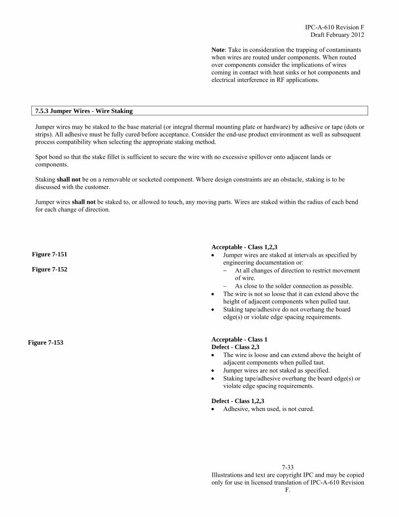
IPC-A-610 Revision F Draft February 2012
7-33 Illustrations and text are copyright IPC and may be copied only for use in licensed translation of IPC-A-610 Revision
F.
Note: Take in consideration the trapping of contaminants when wires are routed under components. When routed over components consider the implications of wires coming in contact with heat sinks or hot components and electrical interference in RF applications.
7.5.3 Jumper Wires - Wire Staking Jumper wires may be staked to the base material (or integral thermal mounting plate or hardware) by adhesive or tape (dots or strips). All adhesive must be fully cured before acceptance. Consider the end-use product environment as well as subsequent process compatibility when selecting the appropriate staking method. Spot bond so that the stake fillet is sufficient to secure the wire with no excessive spillover onto adjacent lands or components. Staking shall not be on a removable or socketed component. Where design constraints are an obstacle, staking is to be discussed with the customer. Jumper wires shall not be staked to, or allowed to touch, any moving parts. Wires are staked within the radius of each bend for each change of direction.
Acceptable - Class 1,2,3 Jumper wires are staked at intervals as specified by
engineering documentation or: At all changes of direction to restrict movement
of wire. As close to the solder connection as possible.
The wire is not so loose that it can extend above the height of adjacent components when pulled taut.
Staking tape/adhesive do not overhang the board edge(s) or violate edge spacing requirements.
Acceptable - Class 1 Defect - Class 2,3 The wire is loose and can extend above the height of
adjacent components when pulled taut. Jumper wires are not staked as specified. Staking tape/adhesive overhang the board edge(s) or
violate edge spacing requirements. Defect - Class 1,2,3 Adhesive, when used, is not cured.
Figure 7-151 Figure 7-152
Figure 7-153

IPC-A-610 Revision F Draft February 2012
7-34 Illustrations and text are copyright IPC and may be copied only for use in licensed translation of IPC-A-610 Revision F.
7.5.4 Jumper Wires - Supported Holes Jumper wires may be attached by any of the following methods. This section is intended to show jumper wire practices that are used in original manufacturing. See IPC-7711/7721 for additional jumper wire information when affecting repairs and modifications. For jumper wires attached to components other than axial leaded, lap solder the wire to the component lead. Assure the solder connection length and insulation clearance meet the minimum/maximum acceptability requirements, see 6.2.3. 7.5.4.1 Jumper Wires - Supported Holes - Lead in Hole
Acceptable - Class 1,2,3 Wires soldered into a PTH/Via hole. Acceptable - Class 1,2 Defect - Class 3 Wire soldered into PTH with component lead.
7.5.5 Jumper Wires - Wrapped Attachment The jumper wire ends are attached to component lead projections by wrapping the wire.
Target – Class 1,2,3 Wire is wrapped 180º to 270º and soldered to a
component lead. Acceptable - Class 1,2,3 Wire is wrapped a minimum of 90 on a flat lead or
180º on a round lead. Acceptable solder connection at wire/lead interface. Wire contour or end is discernible in the solder
connection. Wire overhang of component termination does not
violate minimum electrical clearance. Defect - Class 1,2,3 Wire is wrapped less than 90 on flat or less than
180º on round leads. Wire overhang violates minimum electrical
clearance.
Figure 7-154
Figure 7-155
Figure 7-156 Figure 7-157

IPC-A-610 Revision F Draft February 2012
7-35 Illustrations and text are copyright IPC and may be copied only for use in licensed translation of IPC-A-610 Revision F.
7.5.6 Jumper Wires - Lap Soldered For jumper wires attached to components other than axial leaded, lap solder the wire to the component lead.
Acceptable – Class 1,2,3 Wire is lap soldered to a component lead a
minimum of 75% from edge of land to knee of lead.
Wire is lap soldered to a PTH/via surface. Acceptable solder connection at wire/lead
interface. Wire discernible in the solder. Defect - Class 1,2,3 Wire that is lap soldered is less than 75% from
edge of land to knee of lead. Wire extends beyond the knee of component
lead. Lead violates minimum electrical clearance.
Figure 7-158
Figure 7-159 Figure 7-160 Figure 7-161 Figure 7-162

IPC-A-610 Revision F Draft February 2012
8 Surface Mount Assemblies This section covers acceptability requirements for the fabrication of surface mount assemblies. In this Standard, the words “plastic component” are used in the generic sense to differentiate between plastic components and those made of other materials, e.g., ceramic/alumina or metal (normally hermetically sealed). Some dimensions, e.g., solder thickness, are not inspectable conditions and are identified by notes. Dimension (G) is the solder fillet from the top of the land to the bottom of the termination. Dimension (G) is the prime parameter in the determination of solder connection reliability for leadless components. A thick (G) is desirable. Additional information related to reliability of surface mount connections is available in IPC-D-279, IPC-SM-785 and IPC-9701. Designs with via in land may preclude meeting fillet height criteria. Solder acceptance criteria should be defined between the user and the manufacturer. <Sep2011> In addition to the criteria in this section the criteria of Section 5 are applicable. The following topics are addressed in this section: <Chapter Table of Contents will be added at publication> 8.1 Staking Adhesive 8.1.1 Staking Adhesive – Component Bonding
Target - Class 1, 2, 3 No adhesive present on solderable surfaces of the
termination area. Adhesive is centered between the lands. Acceptable – Class 1 Process Indicator – Class 2 Adhesive material extending from under the
component is visible in the termination area, but end joint width meets minimum requirements.
Defect - Class 3 Adhesive materials extending from under the
component are visible in the termination area.
Figure 8-1
Figure 8-2 Figure 8-3 Figure 8-4

IPC-A-610 Revision F Draft February 2012
8.1.2 Staking Adhesive – Mechanical Strength
Target – Class 1, 2, 3 On SMT components the adhesive is:
50% of the component height. Equal to or greater than 25% of the
circumference. Note: The circumference bonding may have 1 or more
adhesive points. Acceptable – Class 1, 2, 3 On SMT components the adhesive is 25% to 50% of
the component height. Adhesion to the mounting surface is evident. Staking is completely cured and homogenous. Staking is free of voids or bubbles that expose
component conductors or bridge noncommon conductors.
Staking does not prevent stress relief. Acceptable – Class 1 Process Indicator - Class 2, 3 Adhesive on lands or conductive patterns does not
interfere with the formation of solder connection. Not Established – Class 1 Acceptable - Class 2, 3 Rectangular components are staked at each corner of
the component for a minimum 25% to maximum 100% of the height of the component body. (Slight flow under the component body is acceptable provided it does not damage the components or assembly in its intended service environment.)
Figure 8-5 Figure 8-6 IPC ACTION TO CORRECT DWG TO SHOW 25% HEIGHT
Figure 8-7
Figure 8-8
IPC-A-610 Revision F Draft February 2012
Defect – Class 1, 2, 3 On SMT components the adhesive is less than:
25% of the component height. 25 % of the circumference.
There are less than two beads of staking material on an unsleeved vertically mounted component.
Adhesion to the PCB & component surface is not evident.
Required marking is covered. The adhesive interferes with the formation of
required solder connections. Staking is not completely cured and homogenous. Staking voids or bubbles expose component
conductors or bridge noncommon conductors. Staking prevents stress relief. Defect - Class 2, 3 Rectangular components are not staked at each corner
of the component for a minimum 25% to maximum 100% of the height of the component body.
Flow of staking material under the component body will damage the components or assembly in its intended service environment.
8.2 SMT Leads 8.2.1 SMT Leads - Damage These criteria are applicable whether leads are formed manually or by machine or die.
Acceptable - Class 1, 2, 3 No nicks or deformation exceeding 10% of the
diameter, width or thickness of the lead. See 5.2.1 for exposed basis metal criteria.
Defect - Class 1, 2, 3 Lead is damaged or deformed more than 10% of
the diameter, width or thickness of the lead. Lead is deformed from repeated or careless
bending. Heavy indentations such as serrated pliers mark.
Figure 8-9 Figure 8-10

IPC-A-610 Revision F Draft February 2012
8.2.2 SMT Leads - Flattening Components with axial leads of round cross-section may be flattened (coined) for positive seating in surface mounting. Intentionally flattened areas of leads are excluded from the 10% deformation requirement of 8.2.
Acceptable - Class 1, 2 Defect - Class 3 Flattened thickness is less than 40% of the
original diameter.
8.3 SMT Connections SMT connection criteria are provided in 8.3.1 through 8.3.15, as appropriate. 8.3.1 Chip Components - Bottom Only Terminations Discrete chip components, leadless chip carriers, and other devices that have metal terminations on the bottom side only shall meet the dimensional and solder fillet requirements listed below for each product classification. The widths of the component termination and land width are (W) and (P), respectively, and the termination overhang describes the condition where the smaller extends beyond the larger termination (i.e., W or P). The length of the component termination is (R) and the length of the land is (S). Table 8-1 Dimensional Criteria - Chip Component – Bottom Only Termination Features
Feature Dim. Class 1 Class 2 Class 3
Maximum Side Overhang A 50% (W) or 50% (P), whichever is less; Note 1 25% (W) or 25% (P), whichever is less; Note 1
End Overhang B Not permitted Minimum End Joint Width C 50% (W) or 50% (P), whichever is less 75% (W) or 75% (P),
whichever is less Minimum Side Joint Length D Note 3 Maximum Fillet Height E Note 3 Minimum Fillet Height F Note 3 Solder Thickness G Note 3 Minimum End Overlap J Note 3 50% (R) 75% (R) Land Width P Note 2 Termination/Plating Length R Note 2 Land Length S Note 2 Termination Width W Note 2 Note 1. Does not violate minimum electrical clearance. Note 2. Unspecified parameter or variable in size, determined by design. Note 3. Wetting is evident.
IPC-A-610 Revision F Draft February 2012
8.3.1.1 Chip Components - Bottom Only Terminations, Side Overhang (A)
Target - Class 1, 2, 3 No side overhang. Acceptable - Class 1, 2 Side overhang (A) is less than or equal to 50% width
of component termination area (W) or 50% width of land (P), whichever is less.
Acceptable - Class 3 Side overhang (A) is less than or equal to 25% width
of component termination area (W) or 25% width of land (P), whichever is less.
Defect - Class 1, 2 Side overhang (A) is greater than 50% component
termination width (W) or 50% land width (P), whichever is less.
Defect - Class 3 Side overhang (A) is greater than 25% component
termination width (W) or 25% land width (P), whichever is less.
8.3.1.2 Chip Components - Bottom Only Terminations, End Overhang (B)
Defect - Class 1, 2, 3 End overhang (B) in Y axis is not permitted.
Figure 8-11
Figure 8-12

IPC-A-610 Revision F Draft February 2012
8.3.1.3 Chip Components - Bottom Only Terminations, End Joint Width (C)
Target - Class 1, 2, 3 End joint width (C) is equal to the width of the
component termination (W) or width of land (P), whichever is less.
Acceptable - Class 1, 2 Minimum end joint width (C) is 50% width of
component termination (W) or 50% width of land (P), whichever is less.
Acceptable - Class 3 Minimum end joint width (C) is 75% width of
component termination (W) or 75% width of land (P), whichever is less.
Defect - Class 1, 2 End joint width (C) is less than 50% width of
component termination (W) or less than 50% width of land (P), whichever is less.
Defect - Class 3 End joint width (C) is less than 75% width of
component termination (W) or less than 75% width of land (P), whichever is less.
8.3.1.4 Chip Components - Bottom Only Terminations, Side Joint Length (D)
Target - Class 1, 2, 3 Side joint length (D) equals component termination
length (R). Acceptable - Class 1, 2, 3 Any side joint length (D) is acceptable if all other
solder requirements are met.
8.3.1.5 Chip Components - Bottom Only Terminations, Maximum Fillet Height (E) Maximum fillet height (E) requirements are not specified for Class 1, 2, 3. However, wetting is evident.
Defect – Class 1, 2, 3 No wetting evident.
Figure 8-13
Figure 8-14
IPC-A-610 Revision F Draft February 2012
8.3.1.6 Chip Components - Bottom Only Terminations, Minimum Fillet Height (F) Minimum fillet height (F) requirements are not specified for Class 1, 2, 3. However, wetting is evident.
Defect – Class 1, 2, 3 No wetting evident.
8.3.1.7 Chip Components - Bottom Only Terminations, Solder Thickness (G)
Acceptable - Class 1, 2, 3 Wetting is evident. Defect – Class 1, 2, 3 <NEEDS TO BE BELOW FIG 8-16> No wetting evident.
8.3.1.8 Chip Components - Bottom Only Terminations, End Overlap (J)
Acceptable - Class 1 Wetted fillet is evident. Acceptable - Class 2 End overlap (J) between the component termination
and the land is minimum 50% the length of component termination (R).
Acceptable - Class 3 End overlap (J) between the component termination
and the land is a minimum of 75% the length of component termination (R).
Defect - Class 1, 2, 3 Component termination area and land do not overlap.
Defect - Class 2 End overlap (J) is less than 50% of the length of
component termination (R). Defect - Class 3 End overlap (J) is less than 75% of the length of
component termination (R).
Figure 8-15
Figure 8-16
Figure 8-17
IPC-A-610 Revision F Draft February 2012
8.3.2 Rectangular or Square End Chip Components - 1, 3 or 5 Side Terminations These criteria apply to component types such as chip resistor, chip capacitor, network passive parts (R-NET, etc. that have this style of termination) and cylindrical components with square ends. Solder connections to components having terminations of a square or rectangular configuration shall meet the dimensional and solder fillet requirements listed below for each product classification. For 1 sided termination, the solderable side is the vertical end face of the component. Table 8-2 Dimensional Criteria - Rectangular or Square End Chip Components - 1, 3 or 5 Side Terminations
Feature Dim. Class 1 Class 2 Class 3
Maximum Side Overhang A 50% (W) or 50% (P) whichever is less; Note 1 25% (W) or 25% (P) whichever is less; Note 1
End Overhang B Not permitted Minimum End Joint Width C 50% (W) or 50% (P), whichever is less, Note 5 75% (W) or 75% (P),
whichever is less, Note 5Minimum Side Joint Length D Note 3 Maximum fillet Height E Note 4 Minimum Fillet Height F Wetting is evident on the vertical surface(s) of the
component termination. Note 6. (G) + 25% (H) or (G) +
0.5 mm [0.02 in], whichever is less., Note 6
Solder Thickness G Note 3 Termination Height H Note 2 Minimum End Overlap J Required Width of Land P Note 2 Termination Width W Note 2
Side Mounting/Billboarding, Notes 7, 8 Width to Height Ratio Does not exceed 2:1 End Cap and Land Wetting 100% wetting land to end metallization contact areas Minimum End Overlap J 100% Maximum Side Overhang A Not permitted End Overhang B Not permitted Maximum Component Size No limits 1206 Terminations Component has 3 or more wettable termination areas on each end.
Note 1. Does not violate minimum electrical clearance. Note 2. Unspecified dimension, or variable in size as
determined by design. Note 3. Wetting is evident. Note 4. The maximum fillet may overhang the land
and/or extend onto the top of the end cap metallization; however, the solder does not extend further onto the top of the component body.
Note 5: (C) is measured from the narrowest side of the solder fillet.
Note 6: Designs with open, unfilled via in land may preclude meeting these criteria. Solder acceptance criteria should be defined between the user and the manufacturer.<Sep2011>
Note 67: These criteria are for chip components that may flip (rotate) onto the narrow edge during assembly.
Note 78: These criteria may not be acceptable for certain high frequency or high vibration applications.
IPC-A-610 Revision F Draft February 2012
8.3.2.1 Rectangular or Square End Chip Components – 1, 3 or 5 Side Terminations, Side Overhang (A)
Target - Class 1, 2, 3 No side overhang. Acceptable - Class 1, 2 Side overhang (A) is less than or equal to 50%
width of component termination area (W) or 50% width of land (P), whichever is less.
Acceptable - Class 3 Side overhang (A) is less than or equal to 25%
width of component termination area (W) or 25% width of land (P), whichever is less.
8.3.2.1 Rectangular or Square End Chip Components – 1, 3 or 5 Side Terminations, Side Overhang (A) (cont.)
Defect - Class 1, 2 Side overhang (A) is greater than 50% component
termination width (W) or 50% land width (P), whichever is less.
Defect - Class 3 Side overhang (A) is greater than 25% component
termination width (W) or 25% land width (P), whichever is less.
8.3.2.2 Rectangular or Square End Chip Components - 1, 3 or 5 Side Terminations, End Overhang (B)
Target - Class 1, 2, 3 No end overhang. Defect - Class 1, 2, 3 Termination overhangs land.
8.3.2.3 Rectangular or Square End Chip Components - 1, 3 or 5 Side Terminations, End Joint Width (C)
Target - Class 1, 2, 3 End joint width is equal to component termination
width or width of land, whichever is less. Acceptable - Class 1, 2 End joint width (C) is minimum 50% of component
termination width (W) or 50% land width (P), whichever is less.
Figure 8-18
Figure 8-19 1. Class 1, 2 2. Class 3
Figure 8-20
Figure 8-21
Figure 8-22
Figure 8-23
Figure 8-24
Figure 8-25
Figure 8-26
Figure 8-27

IPC-A-610 Revision F Draft February 2012
8.3.2.3 Rectangular or Square End Chip Components - 1, 3 or 5 Side Terminations, End Joint Width (C) (cont.)
Acceptable - Class 3 End joint width (C) is minimum 75% of component
termination (W) or 75% land width (P), whichever is less.
Defect - Class 1, 2, 3 Less than minimum acceptable end joint width.
8.3.2.4 Rectangular or Square End Chip Components - 1, 3 or 5 Side Terminations, Side Joint Length (D)
Target - Class 1, 2, 3 Side joint length equals length of component
termination. Acceptable - Class 1, 2, 3 Side joint length is not required. However, a wetted
fillet is evident. Defect – Class 1, 2, 3 No wetted fillet.
8.3.2.5 Rectangular or Square End Chip Components - 1, 3 or 5 Side Terminations, Maximum Fillet Height (E)
Target - Class 1, 2, 3 Maximum fillet height is the solder thickness plus
component termination height. Acceptable - Class 1,2,3 Maximum fillet height (E) may overhang the land
and/or extend onto the top of the end cap metallization, but not extend further onto the top of component body.
Defect - Class 1,2,3 Solder fillet extends onto the top of the component
body.
Figure 8-28
Figure 8-29
Figure 8-30
Figure 8-31
Figure 8-32
Figure 8-33

IPC-A-610 Revision F Draft February 2012
8.3.2.6 Rectangular or Square End Chip Components - 1, 3 or 5 Side Terminations, Minimum Fillet Height (F)
Acceptable - Class 1, 2
Minimum fillet height (F) exhibits wetting on the vertical surface(s) of the component termination.
Acceptable - Class 3 Minimum fillet height (F) is solder thickness (G) plus
either 25% termination height (H), or 0.5 mm [0.02 in], whichever is less.
Defect – Class 1, 2 No fillet height evident on face of component. Defect - Class 3 Minimum fillet height (F) is less than solder
thickness (G) plus either 25% (H), or solder thickness (G) plus 0.5 mm [0.02 in], whichever is less.
Defect - Class 1, 2, 3 Insufficient solder. A wetted fillet is not evident.
8.3.2.7 Rectangular or Square End Chip Components - 1, 3 or 5 Side Terminations, Solder Thickness (G)
Acceptable - Class 1, 2, 3 Wetted fillet evident. Defect – Class 1, 2, 3 No wetted fillet.
8.3.2.8 Rectangular or Square End Chip Components - 1, 3 or 5 Side Terminations, End Overlap (J)
Acceptable - Class 1,2,3 Evidence of overlap contact (J) between the
component termination and the land is required. Defect - Class 1, 2, 3 Insufficient end overlap.
Figure 8-34
Figure 8-35
Figure 8-36 Figure 8-37
Figure 8-38
Figure 8-39
Figure 8-40 Figure 8-41

IPC-A-610 Revision F Draft February 2012
8.3.2.9 Rectangular or Square End Chip Components - 1, 3 or 5 Side Terminations, Termination Variations 8.3.2.9.1 Rectangular or Square End Chip Components - 1, 3 or 5 Side Terminations, Termination Variations - Mounting on Side (Billboarding) This section provides criteria for chip components that may flip (rotate) onto the narrow edge during assembly. These criteria may not be acceptable for certain high frequency or high vibration applications.
Acceptable - Class 1, 2, 3 Width (W) to height (H) ratio does not exceed two to
one (2:1) ratio; see Figure 8-42. Complete wetting to land and end cap metallization. Overlap contact between 100% of the component
termination (metallization) and the land.
Component has 3 or more termination faces (metallization).
There is evidence of wetting on the 3 vertical faces of the termination area.
Acceptable - Class 1, 2 Component size may be larger than 1206. Defect - Class 1, 2, 3 Width to height ratio exceeds two to one (2:1) ratio. Incomplete wetting of at least 3 component
termination faces to the land. Less than 100% overlap of the component
termination (metallization) and the land. Component overhangs the end or side of the land. Component has less than 3 termination faces
(metallization). Defect - Class 3 Component size is larger than 1206.
Figure 8-42
Figure 8-43
Figure 8-44
Figure 8-45

IPC-A-610 Revision F Draft February 2012
8.3.2.9.2 Rectangular or Square End Chip Components - 1, 3 or 5 Side Terminations, Termination Variations - Mounting Upside Down
Target - Class 1, 2, 3 Element of chip component with exposed deposited
electrical element is mounted away from the board. Acceptable - Class 1 Process Indicator - Class 2, 3 Element of chip component with exposed deposited
electrical element is mounted toward the board.
8.3.2.9.3 Rectangular or Square End Chip Components - 1, 3 or 5 Side Terminations, Termination Variations – Stacking These criteria are applicable when stacking is a requirement. When stacking components, the top termination area of a component becomes the land for the next higher component.
Acceptable - Class 1, 2, 3 When permitted by drawing. Stacking order meet drawing requirements. Stacked components meet the criteria of Table 8-2, for
the applicable class of acceptance. Side overhang does not preclude formation of required
solder fillets. Defect - Class 1, 2, 3 Stacked components when not required by drawing. Stacking order does not meet drawing requirements. Stacked components do not meet the criteria of Table
8-2, for the applicable class of acceptance. Side overhang precludes formation of required solder
fillets.
8.3.2.9.4 Rectangular or Square End Chip Components - 1, 3 or 5 Side Terminations, Termination Variations – Tombstoning
Defect - Class 1, 2, 3 Chip components standing on a terminal end
(tombstoning).
Figure 8-46
Figure 8-47
Figure 8-48
Figure 8-49
Figure 8-50
IPC-A-610 Revision F Draft February 2012
8.3.2.10 Rectangular or Square End Chip Components - 1, 3 or 5 Side Terminations, Termination Variations – 3 Terminations These criteria are also applicable to cylindrical chip components with side terminations, Figure 8-52. 8.3.2.10.1 Rectangular or Square End Chip Components - 1, 3 or 5 Side Terminations, Termination Variations – 3 Terminations – Solder Width
Target - Class 1, 2, 3 End joint width is equal to component
termination width or width of land, whichever is less.
Acceptable - Class 1, 2 End joint width is minimum 50% of component
termination width or 50% land width whichever is less.
Acceptable - Class 3 End joint width is minimum 75% of component
termination or 75% land width whichever is less. Defect - Class 1, 2, 3 Less than minimum acceptable end joint width.
8.3.2.10.2 Rectangular or Square End Chip Components - 1, 3 or 5 Side Terminations, Termination Variations – 3 Terminations – Minimum Fillet Height
Acceptable - Class 1, 2, 3 Wetting is evident on the vertical surface(s) of
the component termination. Defect – Class 1, 2, 3 No fillet height evident on face of component. A wetted fillet is not evident.
Figure 8-51
Figure 8-52
IPC-A-610 Revision F Draft February 2012
8.3.3 Cylindrical End Cap Termination This component is sometimes referred to as MELF (Metal Electrode Leadless Face). Solder connections to components having cylindrical end cap terminations shall meet the dimensional and solder fillet requirements for each product classification. 8.3.2.10 has criteria for cylindrical components that also have side terminations, Figure 8-52. Table 8-3 Dimensional Criteria - Cylindrical End Cap Termination
Feature Dim. Class 1 Class 2 Class 3
Maximum Side Overhang A 25% (W) or 25% (P), whichever is less; Note 1 End Overhang B Not permitted Minimum End Joint Width, Note 2
C Note 4 50% (W) or 50% (P), whichever is less
Minimum Side Joint Length D Notes 4, 6 50% (R) or 50% (S), whichever is less;
Note 6
75% (R) or 75% (S), whichever is less;
Note6 Maximum Fillet Height E Note 5 Minimum Fillet Height (end and side)
F Wetting is evident on the vertical surface(s) of the component termination. Note 7
(G) + 25% (W) or (G) + 1.0 mm [0.0394 in],
whichever is less., Note 7
Solder Thickness G Note 4 Minimum End Overlap J Notes 4, 6 50% (R) Note 6 75% (R) Note 6 Land Width P Note 3 Termination/Plating Length R Note 3 Land Length S Note 3 Termination Diameter W Note 3 Note 1. Does not violate minimum electrical clearance. Note 2. (C) is measured from the narrowest side of the solder fillet. Note 3. Unspecified dimension, or variable in size as determined by design. Note 4. Wetting is evident. Note 5. The maximum fillet may overhang the land or extend onto the top of the component termination; however, the
solder does not extend further onto the component body. Note 6. Does not apply to components with end-only terminations. Note 7. Designs with via in land may preclude meeting those criteria. Solder acceptance criteria should be defined between
the user and the manufacturer.<Sep2011> 8.3.3.1 Cylindrical End Cap Termination, Side Overhang (A)
Target - Class 1, 2, 3 No side overhang. Acceptable - Class 1, 2, 3 Side overhang (A) is 25% or less of the diameter of
component width (W) or land width (P), whichever is less.
Defect - Class 1, 2, 3 Side overhang (A) is greater than 25% of component
diameter, (W), or land width (P), whichever is less.
Figure 8-53
Figure 8-54
Figure 8-55

IPC-A-610 Revision F Draft February 2012
8.3.3.2 Cylindrical End Cap Termination, End Overhang (B)
Target - Class 1, 2, 3 No end overhang (B). Defect - Class 1, 2, 3 Any end overhang (B).
8.3.3.3 Cylindrical End Cap Termination, End Joint Width (C)
Target - Class 1, 2, 3 End joint width is equal to or greater than the
component diameter (W) or width of the land (P), whichever is less.
Acceptable - Class 1 End solder joint exhibits a wetted fillet. Acceptable - Class 2, 3 End joint width (C) is minimum 50% component
diameter (W) or land width (P), whichever is less. Defect - Class 1 End solder joint does not exhibit a wetted fillet. Defect - Class 2, 3 End joint width (C) is less than 50% component
diameter (W), or land width (P), whichever is less.
8.3.3.4 Cylindrical End Cap Termination, Side Joint Length (D)
Target - Class 1, 2, 3 Side joint length (D) is equal to the length of
component termination (R) or land length (S) whichever is less.
Acceptable - Class 1 Side joint length (D) exhibits a wetted fillet. Acceptable - Class 2 Side joint length (D) is minimum 50% length of
component termination (R) or land length (S) whichever is less.
Acceptable - Class 3 Side joint length (D) is minimum 75% length of
component termination (R) or land length (S) whichever is less.
Figure 8-56
Figure 8-57 Figure 8-58 Figure 8-59
Figure 8-60
Figure 8-61
Figure 8-62
IPC-A-610 Revision F Draft February 2012
Defect - Class 1 Side joint length (D) does not exhibit a wetted fillet. Defect - Class 2 Side joint length (D) is less than 50% length of
component termination (R) or land length (S) whichever is less.
Defect - Class 3 Side joint length (D) is less than 75% length of
component termination (R) or land length (S) whichever is less.
8.3.3.5 Cylindrical End Cap Termination, Maximum Fillet Height (E) \
Acceptable - Class 1, 2, 3 Maximum fillet height (E) may overhang the land
and/or extend onto the top of the end cap metallization, but not extend further onto the component body.
Defect - Class 1, 2, 3 Solder fillet extends onto the component body top.
8.3.3.6 Cylindrical End Cap Termination, Minimum Fillet Height (F)
Acceptable - Class 1, 2 Minimum fillet height (F) exhibits wetting on the
vertical surfaces of the component termination. Acceptable - Class 3 Minimum fillet height (F) is solder thickness (G) plus
either 25% diameter (W) of the component end cap or 1.0 mm [0.039 in], whichever is less.
Defect - Class 1, 2, 3 Minimum fillet height (F) does not exhibit wetting. Defect - Class 3 Minimum fillet height (F) is less than the solder
thickness (G) plus either 25% diameter (W) of the component end cap or 1.0 mm [0.039 in], whichever is less.
Figure 8-63
Figure 8-64
Figure 8-65
Figure 8-66
Figure 8-67
IPC-A-610 Revision F Draft February 2012
8.3.3.7 Cylindrical End Cap Termination, Solder Thickness (G)
Acceptable - Class 1, 2, 3 Wetted fillet evident. Defect – Class 1, 2, 3 No wetted fillet.
8.3.3.8 Cylindrical End Cap Termination, End Overlap (J)
Acceptable - Class 1 Wetted fillet is evident. Acceptable - Class 2 End overlap (J) between the component termination
and the land is minimum 50% the length of component termination (R).
Acceptable - Class 3 End overlap (J) between the component termination
and the land is minimum of 75% the length of component termination (R).
Defect - Class 1, 2, 3 Component termination area and land do not overlap. Defect - Class 2 End overlap (J) is less than 50% of the length of
component termination (R). Defect - Class 3 End overlap (J) is less than 75% of the length of
component termination (R).
Figure 8-68
Figure 8-69
Figure 8-70

IPC-A-610 Revision F Draft February 2012
8.3.4 Castellated Terminations Connections formed to castellated terminations of leadless chip components shall meet the dimensional and solder fillet requirements listed below for each product classification. The solder fillet may contact the bottom of the component. Table 8-4 Dimensional Criteria - Castellated Terminations
Feature Dim. Class 1 Class 2 Class 3
Maximum Side Overhang A 50% (W) Note 1 25% (W) Note 1
End Overhang B Not permitted Minimum End Joint Width C 50% (W) 75% (W) Minimum Side Joint Length D Note 3 Depth of castellation Depth of castellationMaximum Fillet Height E Notes 1, 4 Minimum Fillet Height F Note 3 (G) + 25% (H) (G) + 50% (H) Solder Thickness G Note 3 Castellation Height H Note 2 Land Length S Note 2 Castellation Width W Note 2 Note 1. Does not violate minimum electrical clearance. Note 2. Unspecified dimension, or variable in size as determined by design. Note 3. Wetting is evident. Note 4. The maximum fillet may extend past the top of the castellation provided it does not contact the component body.
8.3.4.1 Castellated Terminations, Side Overhang (A)
Target - Class 1, 2, 3 No side overhang. Acceptable - Class 1, 2 Maximum side overhang (A) is 50% castellation
width (W). Acceptable - Class 3 Maximum side overhang (A) is 25% castellation
width (W). Defect - Class 1, 2 Side overhang (A) exceeds 50% castellation
width (W). Defect - Class 3 Side overhang (A) exceeds 25% castellation
width (W).
Figure 8-71
Figure 8-72 1. Leadless chip carrier 2. Castellations (Terminations)
Figure 8-73

IPC-A-610 Revision F Draft February 2012
8.3.4.2 Castellated Terminations, End Overhang (B)
Acceptable – Class 1, 2, 3 No end overhang. Defect - Class 1, 2, 3 End overhang (B).
8.3.4.3 Castellated Terminations, Minimum End Joint Width (C)
Target - Class 1, 2, 3 End joint width (C) is equal to castellation width
(W). Acceptable - Class 1, 2 Minimum end joint width (C) is 50% castellation
width (W). Acceptable - Class 3 Minimum end joint width (C) is 75% castellation
width (W). Defect - Class 1, 2 End joint width (C) is less than 50% castellation
width (W). Defect - Class 3 End joint width (C) is less than 75% castellation
width (W).
8.3.4.4 Castellated Terminations, Minimum Side Joint Length (D)
Acceptable - Class 1 Wetted fillet evident. Acceptable - Class 1, 2, 3 Solder extends from the back of the castellation
onto the land at or beyond the edge of the component.
Defect - Class 1, 2, 3 Wetted fillet not evident. Solder does not extend from the back of the
castellation onto the land at or beyond the edge of the component.
Figure 8-74
Figure 8-75
Figure 8-76

IPC-A-610 Revision F Draft February 2012
8.3.4.5 Castellated Terminations, Maximum Fillet Height (E)
Acceptable – Class 1, 2, 3 The maximum fillet may extend past the top of
the castellation provided it does not extend onto the component body.
Defect – Class 1, 2, 3 Solder fillet violates minimum electrical
clearance. Solder extends past the top of the castellation
onto the component body.
8.3.4.6 Castellated Terminations, Minimum Fillet Height (F)
Acceptable - Class 1 A wetted fillet is evident. Acceptable - Class 2 Minimum fillet height (F) is the solder thickness
(G) (not shown) plus 25% castellation height (H).
Acceptable - Class 3 Minimum fillet height (F) is the solder thickness
(G) (not shown) plus 50% castellation height (H).
Defect - Class 1 A wetted fillet is not evident. Defect - Class 2 Minimum fillet height (F) is less than solder
thickness (G) (not shown) plus 25% castellation height (H).
Defect - Class 3 Minimum fillet height (F) is less than solder
thickness (G) (not shown) plus 50% castellation height (H).
Figure 8-77
Figure 8-78
Figure 8-79
Figure 8-80

IPC-A-610 Revision F Draft February 2012
8.3.4.7 Castellated Terminations, Solder Thickness (G)
Acceptable - Class 1, 2, 3 Wetted fillet evident. Defect – Class 1, 2, 3 No wetted fillet.
8.3.5 Flat Gull Wing Leads Table 8-5 Dimensional Criteria - Flat Gull Wing Leads
Feature Dim. Class 1 Class 2 Class 3
Maximum Side Overhang A 50% (W) or 0.5 mm [0.02 in], whichever is less;
Note 1
25% (W) or 0.5 mm [0.02 in], whichever is
less; Note 1 Maximum Toe Overhang B Note 1 Minimum End Joint Width C 50% (W) 75% (W) Minimum Side Joint Length, Note 6
when (L) is ≥3 W D
1 (W) or 0.5 mm [0.02 in], whichever is less
3 (W) or 75% (L), whichever is longer
when (L) is <3 W 100% (L)
Maximum Heel Fillet Height E Note 4
Minimum Heel Fillet Height
(T) ≤0.38 mm [0.0149 in],
F Note 3
(G) + (T) Note 5 (G) + (T) Note 5
(T) >0.38 mm [0.0149 in],
F (G) + 50% (T) Note 5
Solder Thickness G Note 3 Formed Foot Length L Note 2 Lead Thickness T Note 2 Lead Width W Note 2 Note 1. Does not violate minimum electrical clearance. Note 2. Unspecified dimension, or variable in size as determined by design. Note 3. Wetting is evident. Note 4. See 8.3.5.5 Note 5. In the case of a toe-down lead configuration, the minimum heel fillet height (F) extends at least to the mid-point of
the outside lead bend. Note 6. Fine pitch leads (component terminations on less than 0.65 mm [0.025 in] centers as defined by IPC-T-50) require
a minimum side fillet length of 0.5mm [0.02 in]. 8.3.5.1 Flat Gull Wing Leads, Side Overhang (A)
Target - Class 1, 2, 3 No side overhang. Acceptable - Class 1, 2 Maximum overhang (A) is not greater than 50%
lead width (W) or 0.5 mm [0.02 in], whichever is less.
Acceptable - Class 3
Figure 8-81
Figure 8-82 Figure 8-83
Figure 8-84
IPC-A-610 Revision F Draft February 2012
Maximum overhang (A) is not greater than 25%
lead width (W) or 0.5 mm [0.02 in], whichever is less.
Defect - Class 1, 2 Side overhang (A) is greater than 50% lead
width (W) or 0.5 mm [0.02 in], whichever is less.
Defect - Class 3 Side overhang (A) is greater than 25% lead
width (W) or 0.5 mm [0.02 in], whichever is less.
8.3.5.2 Flat Gull Wing Leads, Toe Overhang (B)
Acceptable - Class 1, 2, 3 Toe overhang does not violate minimum
electrical clearance. Defect - Class 1, 2, 3 Toe overhang violates minimum electrical
clearance.
8.3.5.3 Flat Gull Wing Leads, Minimum End Joint Width (C)
Target - Class 1, 2, 3 End joint width is equal to or greater than lead
width. Acceptable - Class 1, 2 Minimum end joint width (C) is 50% lead width
(W).
8.3.5.3 Flat Gull Wing Leads, Minimum End Joint Width (C) (cont.)
Acceptable - Class 3 Minimum end joint width (C) is 75% lead width
(W). Defect - Class 1, 2 Minimum end joint width (C) is less than 50%
lead width (W). Defect - Class 3
Figure 8-85
Figure 8-86
Figure 8-87
Figure 8-88
Figure 8-89
Figure 8-90
Figure 8-91
Figure 8-92

IPC-A-610 Revision F Draft February 2012
Minimum end joint width (C) is less than 75%
lead width (W).
8.3.5.4 Flat Gull Wing Leads, Minimum Side Joint Length (D)
Target - Class 1, 2, 3 Evidence of wetted fillet along full length of lead
foot.
8.3.5.4 Flat Gull Wing Leads, Minimum Side Joint Length (D) (cont.)
Acceptable - Class 1 Minimum side joint length (D) is equal to lead
width (W) or 0.5 mm [0.02 in], whichever is less (not shown).
Acceptable - Class 2, 3 When foot length (L) is less than 3 lead widths
(W), minimum side joint length (D) is equal to 100% (L), Figure 8-96.
When foot length (L) is greater than 3 lead widths (W), minimum side joint length (D) is equal to or greater than 3 lead widths (W), Figure 8-97.
Defect - Class 1 Minimum side joint length (D) is less than the
lead width (W) or 0.5 mm [0.02 in], whichever is less.
Defect - Class 2, 3 When foot length (L) is greater than 3 lead
widths (W), minimum side joint length (D) is less than 3 lead widths (W) or 75% (L), whichever is longer.
When foot length (L) is less than 3 lead widths (W), minimum side joint length (D) is less than 100% (L).
Figure 8-93
Figure 8-94
Figure 8-95
Figure 8-96
Figure 8-97
Figure 8-98

IPC-A-610 Revision F Draft February 2012
8.3.5.5 Flat Gull Wing Leads, Maximum Heel Fillet Height (E) In the following criteria, the words “plastic component” are used in the generic sense to differentiate between plastic components and those made of other materials, e.g., ceramic/alumina or metal (normally hermetically sealed).
Target - Class 1, 2, 3 Heel fillet extends above lead thickness but does
not fill upper lead bend. Solder does not contact the component body. Acceptable – Class 1, 2, 3 Solder touches a plastic SOIC or SOT
component. Solder does not touch ceramic or metal
component. Acceptable - Class 1 Defect – Class 2, 3 Solder touches the body of a plastic component,
except for SOICs and SOTs. Solder touches the body of a ceramic or metal
component.
8.3.5.6 Flat Gull Wing Leads, Minimum Heel Fillet Height (F)
Target – Class 1, 2, 3 Heel fillet height (F) is greater than solder
thickness (G) plus lead thickness (T) but does not extend into knee bend radius.
Acceptable - Class 1 A wetted fillet is evident. Acceptable - Class 2 Where (T) is equal to or less than 0.38 mm
[0.0149 in], the minimum heel fillet is (G) + (T). Where (T) is greater 0.38 mm [0.0149 in], the
minimum heel fillet is (G) + 50% (T). Acceptable - Class 3 Minimum heel fillet height (F) is equal to solder
thickness (G) plus lead thickness (T) at connection side.
Acceptable - Class 1, 2, 3 In the case of a toe-down configuration (not
shown), the minimum heel fillet height (F) extends at least to the mid-point of the outside lead bend.
Figure 8-99 Figure 8-100
Figure 8-101
Figure 8-102
Figure 8-103
Figure 8-104
Figure 8-105
IPC-A-610 Revision F Draft February 2012
Defect - Class 1 A wetted fillet is not evident. Defect - Class 2 Where (T) is equal to or less than 0.38 mm
[0.0149 in], the minimum heel fillet is less than (G) + (T).
Where (T) is greater than 0.38 mm [0.0149 in], the minimum heel fillet is less than (G) + 50% (T).
Minimum heel fillet height (F) is less than solder thickness (G) plus 50% lead thickness (T) at connection side.
Defect - Class 3 Minimum heel fillet height (F) is less than solder
thickness (G) plus lead thickness (T) at connection side.
Defect - Class 1, 2, 3 In the case of a toe-down configuration, the
minimum heel fillet height (F) does not extend at least to the mid-point of the outside lead bend.
8.3.5.7 Flat Gull Wing Leads, Solder Thickness (G)
Acceptable - Class 1, 2, 3 Wetted fillet evident. Defect – Class 1, 2, 3 No wetted fillet.
8.3.5.8 Flat Gull Wing Leads, Coplanarity
Defect - Class 1, 2, 3 Component lead(s) out of alignment
(coplanarity) preventing the formation of an acceptable solder connection.
Figure 8-106
Figure 8-107
Figure 8-108
Figure 8-109
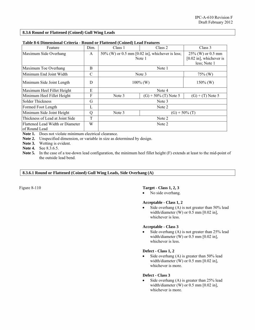
IPC-A-610 Revision F Draft February 2012
8.3.6 Round or Flattened (Coined) Gull Wing Leads Table 8-6 Dimensional Criteria - Round or Flattened (Coined) Lead Features
Feature Dim. Class 1 Class 2 Class 3
Maximum Side Overhang A 50% (W) or 0.5 mm [0.02 in], whichever is less; Note 1
25% (W) or 0.5 mm [0.02 in], whichever is
less; Note 1 Maximum Toe Overhang B Note 1
Minimum End Joint Width C Note 3 75% (W)
Minimum Side Joint Length D 100% (W) 150% (W)
Maximum Heel Fillet Height E Note 4 Minimum Heel Fillet Height F Note 3 (G) + 50% (T) Note 5 (G) + (T) Note 5 Solder Thickness G Note 3 Formed Foot Length L Note 2 Minimum Side Joint Height Q Note 3 (G) + 50% (T) Thickness of Lead at Joint Side T Note 2 Flattened Lead Width or Diameter of Round Lead
W Note 2
Note 1. Does not violate minimum electrical clearance. Note 2. Unspecified dimension, or variable in size as determined by design. Note 3. Wetting is evident. Note 4. See 8.3.6.5. Note 5. In the case of a toe-down lead configuration, the minimum heel fillet height (F) extends at least to the mid-point of
the outside lead bend. 8.3.6.1 Round or Flattened (Coined) Gull Wing Leads, Side Overhang (A)
Target - Class 1, 2, 3 No side overhang. Acceptable - Class 1, 2 Side overhang (A) is not greater than 50% lead
width/diameter (W) or 0.5 mm [0.02 in], whichever is less.
Acceptable - Class 3 Side overhang (A) is not greater than 25% lead
width/diameter (W) or 0.5 mm [0.02 in], whichever is less.
Defect - Class 1, 2 Side overhang (A) is greater than 50% lead
width/diameter (W) or 0.5 mm [0.02 in], whichever is more.
Defect - Class 3 Side overhang (A) is greater than 25% lead
width/diameter (W) or 0.5 mm [0.02 in], whichever is more.
Figure 8-110

IPC-A-610 Revision F Draft February 2012
8.3.6.2 Round or Flattened (Coined) Gull Wing Leads, Toe Overhang (B)
Acceptable - Class 1, 2, 3 Toe overhang (B) is not specified. Does not violate minimum electrical clearance. Defect - Class 1, 2, 3 Toe overhang violates minimum electrical
clearance.
8.3.6.3 Round or Flattened (Coined) Gull Wing Leads, Minimum End Joint Width (C)
Target - Class 1, 2, 3 End joint width (C) is equal to or greater than
lead width/diameter (W). Acceptable - Class 1, 2 Wetted fillet is evident. Acceptable - Class 3 End joint width (C) is minimum 75% lead
width/diameter (W). Defect - Class 1, 2 No evidence of wetted fillet. Defect - Class 3 Minimum end joint width (C) is less than 75%
lead width/diameter (W).
8.3.6.4 Round or Flattened (Coined) Gull Wing Leads, Minimum Side Joint Length (D)
Acceptable - Class 1, 2 Side joint length (D) is equal to lead
width/diameter (W). Acceptable - Class 3 Minimum side joint length (D) is equal to 150%
lead width/diameter (W). Defect - Class 1, 2 Side joint length (D) is less than lead
width/diameter (W). Defect - Class 3 Minimum side joint length (D) is less than 150%
the lead width/diameter (W).
Figure 8-111
Figure 8-112
Figure 8-113

IPC-A-610 Revision F Draft February 2012
8.3.6.5 Round or Flattened (Coined) Gull Wing Leads, Maximum Heel Fillet Height (E) In the following criteria, the words “plastic component” are used in the generic sense to differentiate between plastic components and those made of other materials, e.g., ceramic/alumina or metal (normally hermetically sealed).
Target – Class 1, 2, 3 Heel fillet extends above lead thickness but does
not fill upper lead bend. Solder does not contact the component body. Acceptable - Class 1, 2, 3 Solder touches the body of a plastic SOIC or
SOT component. Solder does not touch body of ceramic or metal
component. Defect - Class 1 A wetted fillet is not evident. Acceptable – Class 1 Defect - Class 2, 3 Solder touches the body of a plastic component,
except for SOICs and SOTs. Solder touches the body of ceramic or metal
component. Defect - Class 1, 2, 3 Solder is excessive so that the minimum
electrical clearance is violated.
8.3.6.6 Round or Flattened (Coined) Gull Wing Leads, Minimum Heel Fillet Height (F)
Acceptable - Class 1, 2, 3 In the case of a toe-down configuration (not
shown), the minimum heel fillet height (F) extends at least to the mid-point of the outside lead bend.
Acceptable - Class 1 A wetted fillet is evident. Acceptable - Class 2 Minimum heel fillet height (F) is equal to solder
thickness (G) plus 50% thickness of lead at joint side (T).
Acceptable - Class 3 Minimum heel fillet height (F) is equal to solder
thickness (G) plus thickness of lead at joint side (T).
Figure 8-114
Figure 8-115
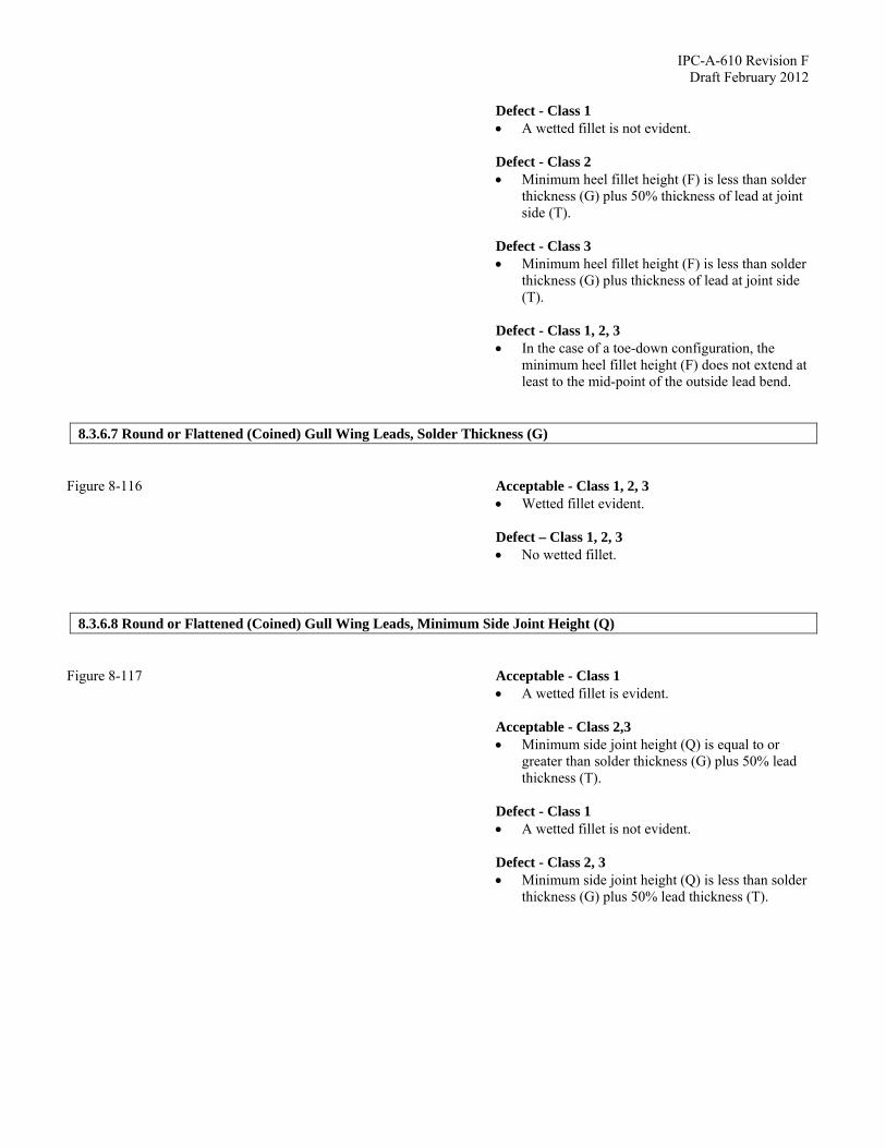
IPC-A-610 Revision F Draft February 2012
Defect - Class 1 A wetted fillet is not evident. Defect - Class 2 Minimum heel fillet height (F) is less than solder
thickness (G) plus 50% thickness of lead at joint side (T).
Defect - Class 3 Minimum heel fillet height (F) is less than solder
thickness (G) plus thickness of lead at joint side (T).
Defect - Class 1, 2, 3 In the case of a toe-down configuration, the
minimum heel fillet height (F) does not extend at least to the mid-point of the outside lead bend.
8.3.6.7 Round or Flattened (Coined) Gull Wing Leads, Solder Thickness (G)
Acceptable - Class 1, 2, 3 Wetted fillet evident. Defect – Class 1, 2, 3 No wetted fillet.
8.3.6.8 Round or Flattened (Coined) Gull Wing Leads, Minimum Side Joint Height (Q)
Acceptable - Class 1 A wetted fillet is evident. Acceptable - Class 2,3 Minimum side joint height (Q) is equal to or
greater than solder thickness (G) plus 50% lead thickness (T).
Defect - Class 1 A wetted fillet is not evident. Defect - Class 2, 3 Minimum side joint height (Q) is less than solder
thickness (G) plus 50% lead thickness (T).
Figure 8-116
Figure 8-117
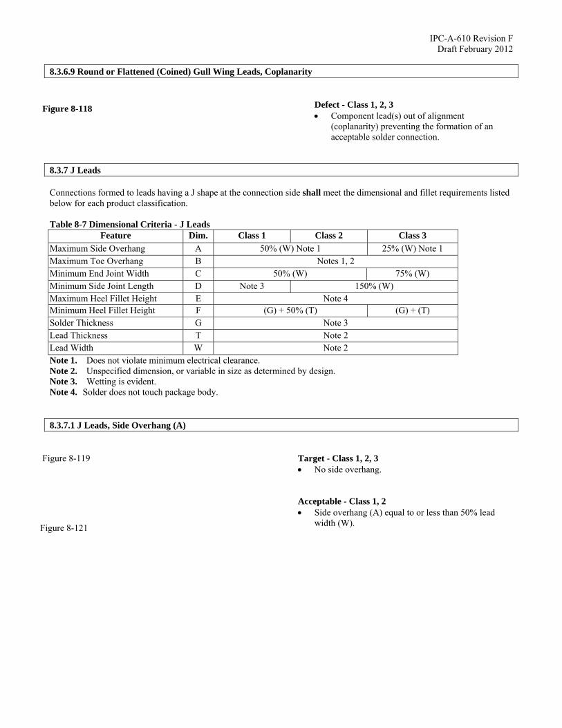
IPC-A-610 Revision F Draft February 2012
8.3.6.9 Round or Flattened (Coined) Gull Wing Leads, Coplanarity
Defect - Class 1, 2, 3 Component lead(s) out of alignment
(coplanarity) preventing the formation of an acceptable solder connection.
8.3.7 J Leads Connections formed to leads having a J shape at the connection side shall meet the dimensional and fillet requirements listed below for each product classification. Table 8-7 Dimensional Criteria - J Leads
Feature Dim. Class 1 Class 2 Class 3
Maximum Side Overhang A 50% (W) Note 1 25% (W) Note 1 Maximum Toe Overhang B Notes 1, 2 Minimum End Joint Width C 50% (W) 75% (W) Minimum Side Joint Length D Note 3 150% (W) Maximum Heel Fillet Height E Note 4 Minimum Heel Fillet Height F (G) + 50% (T) (G) + (T) Solder Thickness G Note 3 Lead Thickness T Note 2 Lead Width W Note 2 Note 1. Does not violate minimum electrical clearance. Note 2. Unspecified dimension, or variable in size as determined by design. Note 3. Wetting is evident. Note 4. Solder does not touch package body. 8.3.7.1 J Leads, Side Overhang (A)
Target - Class 1, 2, 3 No side overhang. Acceptable - Class 1, 2 Side overhang (A) equal to or less than 50% lead
width (W).
Figure 8-118
Figure 8-119
Figure 8-121

IPC-A-610 Revision F Draft February 2012
8.3.7.1 J Leads, Side Overhang (A) (cont.)
Acceptable - Class 3 Side overhang (A) equal to or less than 25% lead
width (W). Defect - Class 1, 2 Side overhang exceeds 50% lead width (W). Defect - Class 3 Side overhang exceeds 25% lead width (W).
8.3.7.2 J Leads, Toe Overhang (B)
Acceptable - Class 1, 2, 3 Toe overhang (B) is an unspecified parameter.
8.3.7.3 J Leads, End Joint Width (C)
Target - Class 1, 2, 3 End joint width (C) is equal to or greater than lead
width (W).
8.3.7.3 J Leads, End Joint Width (C) (cont.)
Acceptable - Class 1, 2 Minimum end joint width (C) is 50% lead width (W). Acceptable - Class 3 Minimum end joint width (C) is 75% lead width (W). Defect - Class 1, 2 Minimum end joint width (C) is less than 50% lead
width (W). Defect - Class 3 Minimum end joint width (C) is less than 75% lead
width (W).
Figure 8-120
Figure 8-122 Figure 8-123
Figure 8-124
Figure 8-125
Figure 8-126
Figure 8-127
Figure 8-128
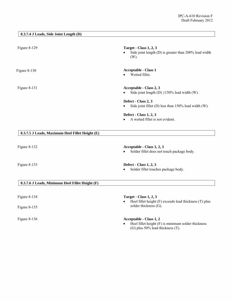
IPC-A-610 Revision F Draft February 2012
8.3.7.4 J Leads, Side Joint Length (D)
Target - Class 1, 2, 3 Side joint length (D) is greater than 200% lead width
(W). Acceptable - Class 1 Wetted fillet. Acceptable - Class 2, 3 Side joint length (D) ≥150% lead width (W). Defect - Class 2, 3 Side joint fillet (D) less than 150% lead width (W). Defect - Class 1, 2, 3 A wetted fillet is not evident.
8.3.7.5 J Leads, Maximum Heel Fillet Height (E)
Acceptable - Class 1, 2, 3 Solder fillet does not touch package body. Defect - Class 1, 2, 3 Solder fillet touches package body.
8.3.7.6 J Leads, Minimum Heel Fillet Height (F)
Target - Class 1, 2, 3 Heel fillet height (F) exceeds lead thickness (T) plus
solder thickness (G). Acceptable - Class 1, 2 Heel fillet height (F) is minimum solder thickness
(G) plus 50% lead thickness (T).
Figure 8-129
Figure 8-130
Figure 8-131
Figure 8-132
Figure 8-133
Figure 8-134
Figure 8-135
Figure 8-136

IPC-A-610 Revision F Draft February 2012
8.3.7.6 J Leads, Minimum Heel Fillet Height (F) (cont.)
Acceptable - Class 3 Heel fillet height (F) is at least lead thickness (T) plus
solder thickness (G). Defect - Class 1, 2, 3 Heel fillet not wetted. Defect - Class 1, 2 Heel fillet height (F) less than solder thickness (G)
plus 50% lead thickness (T). Defect - Class 3 Heel fillet height (F) less than solder thickness (G)
plus lead thickness (T).
8.3.7.7 J Leads, Solder Thickness (G)
Acceptable - Class 1, 2, 3 Wetted fillet evident. Defect – Class 1, 2, 3 No wetted fillet.
8.3.7.8 J Leads, Coplanarity
Defect - Class 1, 2, 3 Component lead(s) out of alignment (coplanarity)
preventing the formation of an acceptable solder connection.
Figure 8-137
Figure 8-138
Figure 8-139
Figure 8-140

IPC-A-610 Revision F Draft February 2012
8.3.8 Butt/I Connections Connections formed to leads positioned perpendicular to a circuit land in a butt configuration shall meet dimensional and solder fillet requirements in Table 8-8. Post assembly acceptability evaluations should consider the inherent limitation of this component mounting technique to survive operational environments when compared to footed leads or through hole mounting. For Class 1 and 2 product, leads not having wettable sides by design (such as leads stamped or sheared from pre-plated stock) are not required to have side fillets. However the design should permit easy inspection of wetting to the wettable surfaces. Butt connections are not permitted for Class 3 products. Table 8-8 Dimensional Criteria – Butt/I Connections
Feature Dim. Class 1 Class 2
Maximum Side Overhang A 25% (W) Note 1 Not permitted Toe Overhang B Not permitted Minimum End Joint Width C 75% (W) Minimum Side Joint Length D Note 2 Maximum Fillet Height E Note 4 Minimum Fillet Height F 0.5 mm [0.0197 in] Solder Thickness G Note 3 Lead Thickness T Note 2 Lead Width W Note 2 Note 1. Does not violate minimum electrical clearance. Note 2. Unspecified dimension, or variable in size as determined by design. Note 3. Wetting is evident. Note 4. Maximum fillet may extend into the bend radius. Solder does not touch package body. 8.3.8.1 Butt/I Connections, Maximum Side Overhang (A)
Target - Class 1, 2 No side overhang. Acceptable - Class 1 Overhang (A) less than 25% lead width (W). Defect - Class 1 Overhang (A) exceeds 25% lead width (W). Defect - Class 2 Any side overhang (A).
8.3.8.2 Butt/I Connections, Maximum Toe Overhang (B)
Defect - Class 1, 2 Any toe overhang (B).
Figure 8-141
Figure 12-142
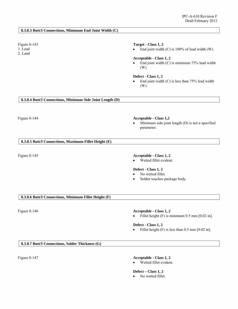
IPC-A-610 Revision F Draft February 2012
8.3.8.3 Butt/I Connections, Minimum End Joint Width (C)
Target - Class 1, 2 End joint width (C) is 100% of lead width (W). Acceptable - Class 1, 2 End joint width (C) is minimum 75% lead width
(W). Defect - Class 1, 2 End joint width (C) is less than 75% lead width
(W).
8.3.8.4 Butt/I Connections, Minimum Side Joint Length (D)
Acceptable - Class 1,2 Minimum side joint length (D) is not a specified
parameter.
8.3.8.5 Butt/I Connections, Maximum Fillet Height (E)
Acceptable - Class 1, 2 Wetted fillet evident. Defect - Class 1, 2 No wetted fillet. Solder touches package body.
8.3.8.6 Butt/I Connections, Minimum Fillet Height (F)
Acceptable - Class 1, 2 Fillet height (F) is minimum 0.5 mm [0.02 in]. Defect - Class 1, 2 Fillet height (F) is less than 0.5 mm [0.02 in].
8.3.8.7 Butt/I Connections, Solder Thickness (G)
Acceptable - Class 1, 2 Wetted fillet evident. Defect – Class 1, 2 No wetted fillet.
Figure 8-143 1. Lead 2. Land
Figure 8-144
Figure 8-145
Figure 8-146
Figure 8-147

IPC-A-610 Revision F Draft February 2012
8.3.9 Flat Lug Leads Connections formed to the leads of power dissipating components with flat lug leads shall meet the dimensional requirements of Table 8-9 and Figure 8-149. The design should permit easy inspection of wetting to the wettable surfaces. Non-conformance to the requirements of Table 8-9 is a defect. Table 8-9 Dimensional Criteria - Flat Lug Leads Feature Dim. Class 1 Class 2 Class 3 Maximum Side Overhang A 50% (W) Note 1 25% (W) Note 1 Not permitted Maximum Toe Overhang B Note 1 Not permitted Minimum end Joint Width C 50% (W) 75% (W) (W) Minimum Side Joint Length
D Note 3 (L)-(M), Note4
Maximum Fillet Height E Note 2 (G) + (T) + 1.0 mm
[0.039 in] Minimum Fillet Height F Note 3 (G) + (T) Solder Fillet Thickness G Note 3 Lead Length L Note 2 Maximum Gap M Note 2 Land Width P Note 2 Lead Thickness T Note 2 Lead Width W Note 2 Note 1. Does not violate minimum electrical clearance. Note 2. Unspecified parameter or variable in size as determined by design. Note 3. Wetted fillet is evident. Note 4. Where the lug is intended to be soldered beneath the component body and the land is designed for the purpose, the
lead shows evidence of wetting in the gap M.
Defect – Class 1, 2, 3 Side overhang does not meet Table 8-9.
Figure 8-148 Figure 8-149 Figure 8-150
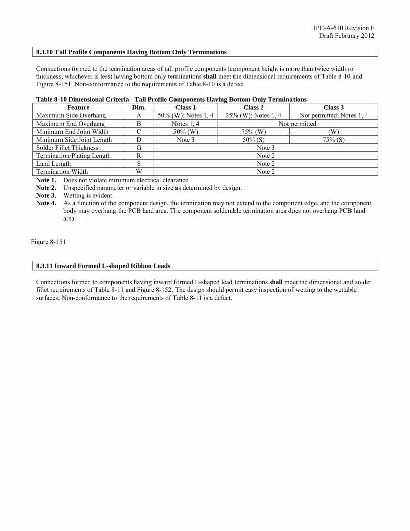
IPC-A-610 Revision F Draft February 2012
8.3.10 Tall Profile Components Having Bottom Only Terminations Connections formed to the termination areas of tall profile components (component height is more than twice width or thickness, whichever is less) having bottom only terminations shall meet the dimensional requirements of Table 8-10 and Figure 8-151. Non-conformance to the requirements of Table 8-10 is a defect. Table 8-10 Dimensional Criteria - Tall Profile Components Having Bottom Only Terminations
Feature Dim. Class 1 Class 2 Class 3 Maximum Side Overhang A 50% (W); Notes 1, 4 25% (W); Notes 1, 4 Not permitted; Notes 1, 4 Maximum End Overhang B Notes 1, 4 Not permitted Minimum End Joint Width C 50% (W) 75% (W) (W) Minimum Side Joint Length D Note 3 50% (S) 75% (S) Solder Fillet Thickness G Note 3 Termination/Plating Length R Note 2 Land Length S Note 2 Termination Width W Note 2 Note 1. Does not violate minimum electrical clearance. Note 2. Unspecified parameter or variable in size as determined by design. Note 3. Wetting is evident. Note 4. As a function of the component design, the termination may not extend to the component edge, and the component
body may overhang the PCB land area. The component solderable termination area does not overhang PCB land area.
8.3.11 Inward Formed L-shaped Ribbon Leads Connections formed to components having inward formed L-shaped lead terminations shall meet the dimensional and solder fillet requirements of Table 8-11 and Figure 8-152. The design should permit easy inspection of wetting to the wettable surfaces. Non-conformance to the requirements of Table 8-11 is a defect.
Figure 8-151
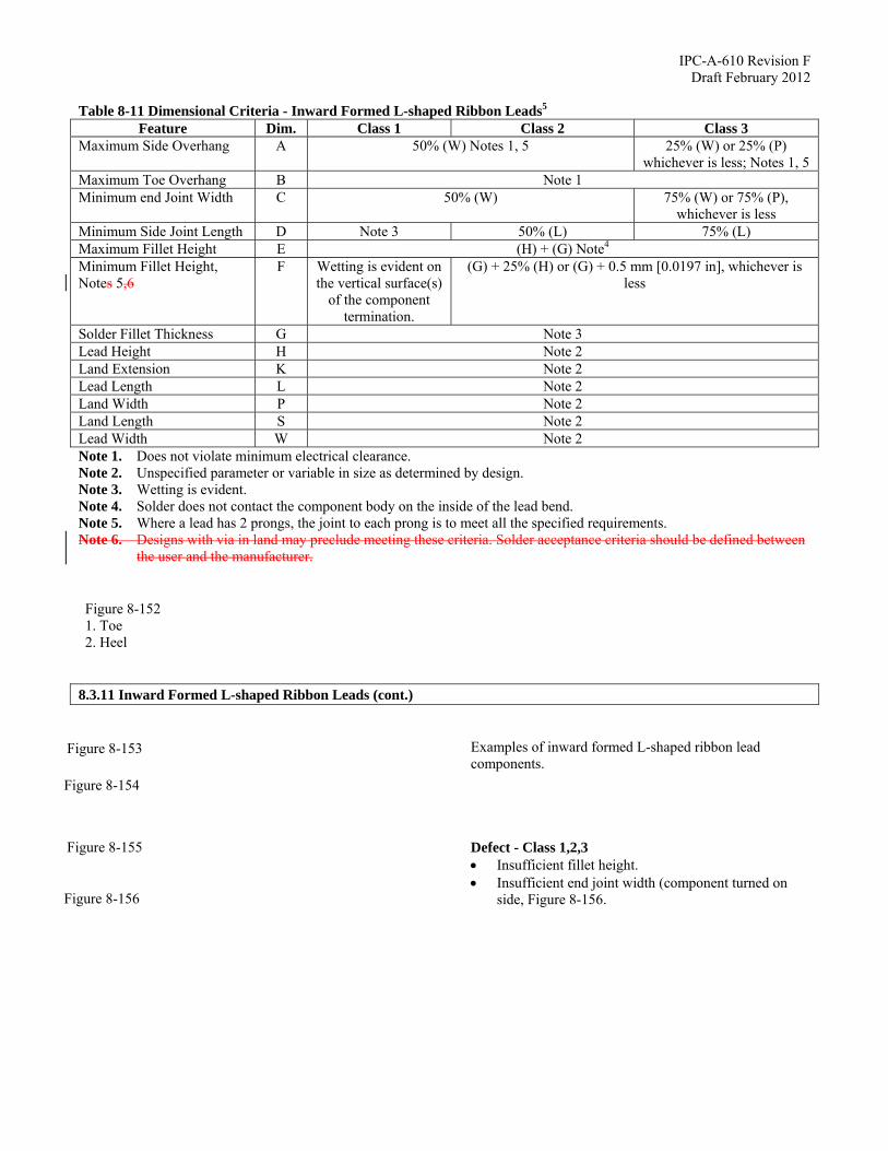
IPC-A-610 Revision F Draft February 2012
Table 8-11 Dimensional Criteria - Inward Formed L-shaped Ribbon Leads5
Feature Dim. Class 1 Class 2 Class 3Maximum Side Overhang A 50% (W) Notes 1, 5 25% (W) or 25% (P)
whichever is less; Notes 1, 5
Maximum Toe Overhang B Note 1Minimum end Joint Width C 50% (W) 75% (W) or 75% (P),
whichever is less
Minimum Side Joint Length D Note 3 50% (L) 75% (L)Maximum Fillet Height E (H) + (G) Note4
Minimum Fillet Height, Notes 5,6
F Wetting is evident on the vertical surface(s)
of the component termination.
(G) + 25% (H) or (G) + 0.5 mm [0.0197 in], whichever is less
Solder Fillet Thickness G Note 3 Lead Height H Note 2 Land Extension K Note 2 Lead Length L Note 2 Land Width P Note 2 Land Length S Note 2 Lead Width W Note 2 Note 1. Does not violate minimum electrical clearance. Note 2. Unspecified parameter or variable in size as determined by design. Note 3. Wetting is evident. Note 4. Solder does not contact the component body on the inside of the lead bend. Note 5. Where a lead has 2 prongs, the joint to each prong is to meet all the specified requirements. Note 6. Designs with via in land may preclude meeting these criteria. Solder acceptance criteria should be defined between
the user and the manufacturer.
8.3.11 Inward Formed L-shaped Ribbon Leads (cont.)
Examples of inward formed L-shaped ribbon lead components. Defect - Class 1,2,3 Insufficient fillet height. Insufficient end joint width (component turned on
side, Figure 8-156.
Figure 8-152 1. Toe 2. Heel
Figure 8-153
Figure 8-154
Figure 8-155
Figure 8-156
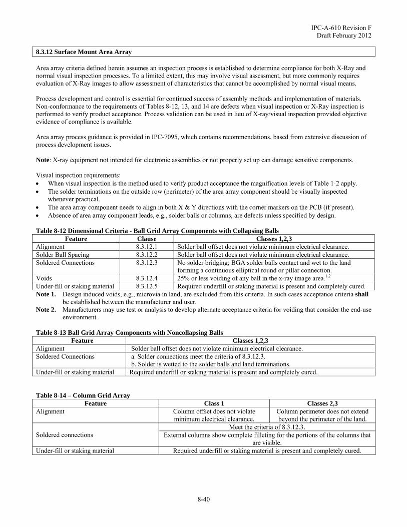
IPC-A-610 Revision F Draft February 2012
8-40
8.3.12 Surface Mount Area Array Area array criteria defined herein assumes an inspection process is established to determine compliance for both X-Ray and normal visual inspection processes. To a limited extent, this may involve visual assessment, but more commonly requires evaluation of X-Ray images to allow assessment of characteristics that cannot be accomplished by normal visual means. Process development and control is essential for continued success of assembly methods and implementation of materials. Non-conformance to the requirements of Tables 8-12, 13, and 14 are defects when visual inspection or X-Ray inspection is performed to verify product acceptance. Process validation can be used in lieu of X-ray/visual inspection provided objective evidence of compliance is available. Area array process guidance is provided in IPC-7095, which contains recommendations, based from extensive discussion of process development issues. Note: X-ray equipment not intended for electronic assemblies or not properly set up can damage sensitive components. Visual inspection requirements: When visual inspection is the method used to verify product acceptance the magnification levels of Table 1-2 apply. The solder terminations on the outside row (perimeter) of the area array component should be visually inspected
whenever practical. The area array component needs to align in both X & Y directions with the corner markers on the PCB (if present). Absence of area array component leads, e.g., solder balls or columns, are defects unless specified by design. Table 8-12 Dimensional Criteria - Ball Grid Array Components with Collapsing Balls
Feature Clause Classes 1,2,3 Alignment 8.3.12.1 Solder ball offset does not violate minimum electrical clearance. Solder Ball Spacing 8.3.12.2 Solder ball offset does not violate minimum electrical clearance. Soldered Connections 8.3.12.3 No solder bridging; BGA solder balls contact and wet to the land
forming a continuous elliptical round or pillar connection. Voids 8.3.12.4 25% or less voiding of any ball in the x-ray image area.1,2 Under-fill or staking material 8.3.12.5 Required underfill or staking material is present and completely cured. Note 1. Design induced voids, e.g., microvia in land, are excluded from this criteria. In such cases acceptance criteria shall
be established between the manufacturer and user. Note 2. Manufacturers may use test or analysis to develop alternate acceptance criteria for voiding that consider the end-use
environment. Table 8-13 Ball Grid Array Components with Noncollapsing Balls
Feature Classes 1,2,3 Alignment Solder ball offset does not violate minimum electrical clearance. Soldered Connections a. Solder connections meet the criteria of 8.3.12.3.
b. Solder is wetted to the solder balls and land terminations. Under-fill or staking material Required underfill or staking material is present and completely cured. Table 8-14 – Column Grid Array
Feature Class 1 Classes 2,3 Alignment Column offset does not violate
minimum electrical clearance. Column perimeter does not extend beyond the perimeter of the land.
Soldered connections Meet the criteria of 8.3.12.3.
External columns show complete filleting for the portions of the columns that are visible.
Under-fill or staking material Required underfill or staking material is present and completely cured.
IPC-A-610 Revision F Draft February 2012
8-41
8.3.12.1 Surface Mount Area Array - Alignment
Target - Class 1, 2, 3 Placement of the BGA solder ball is centered and
shows no offset of the ball to land centers. Defect – Class 1, 2, 3 Solder ball offset violates minimum electrical clearance.
8.3.12.2 Surface Mount Area Array - Solder Ball Spacing
Acceptable – Class 1, 2, 3 BGA Solder balls do not violate minimum
electrical clearance (C). Defect – Class 1, 2, 3 BGA solder ball spacing violates minimum
electrical clearance.
8.3.12.3 Surface Mount Area Array - Solder Connections
Target – Class 1, 2, 3 The BGA solder ball terminations are uniform in
size and shape. Acceptable – Class 1, 2, 3 No solder bridging. BGA solder balls contact and wet to the land
forming a continuous elliptical round or pillar connection, Figures 8-157, 158.
Process Indicator – Class 2, 3 BGA solder ball terminations are not uniform in
size, shape, coloration, and color contrast. Defect – Class 1, 2, 3 Visual or x-ray evidence of solder bridging,
Figure 8-159. A “waist” in the solder connection indicating that
the solder ball and the attaching solder paste did not flow together. Figure 8-160.
Incomplete wetting to the land. BGA solder ball terminations have incomplete
reflow of the solder paste, Figure 8-161. Fractured solder connection, Figure 8-162. Ball is not wetted to solder (head in pillow/head
on pillow), Figure 8-163 arrow.
Figure 8-157
Figure 8-158
Figure 8-159 Figure 8-160 Figure 8-161 Figure 8-162 Figure 8-163

IPC-A-610 Revision F Draft February 2012
8-42
8.3.12.4 Surface Mount Area Array - Voids Design induced voids, e.g., microvia in land, are excluded from this criteria. In such cases acceptance criteria shall be established between the manufacturer and user. Manufacturers may use test or analysis to develop alternate acceptance criteria for voiding that consider the end-use environment. -----Original Message----- From: Burnette Terry-RA0528 [mailto:[email protected]] Sent: Thursday, January 27, 2011 11:10 AM To: answers Subject: RE: IPC610 BGA void spec Jack, Thank you for answering. I'm still not clear on why the term defect is used rather than the term process indicator. You mention comments and support data. You and I have communicated a number of times on this subject over the years. When the IPC first proposed a void spec I sent you the enclosed study which to my knowledge was the only reliability study in the industry at the time that looked at the effects of BGA solder joint voids. Even though our data showed no reliability issues due to voids IPC implemented a 25% max. void spec where the voids were referred to as defects. Since then Cisco, Intel, and even the IPC Solder Product Value Council have published similar studies which verified the original Motorola results. I have a unique two fold job. My lab performs the PCB level solder joint reliability testing on all new semiconductor packages. Our primary test methods are air-air temp cycle, liquid-liquid thermal shock, drop, and bend testing. We often perform SJR testing with and for many of our larger customers on their actual products. Since we first introduced BGA over 17 years ago I'd estimate we have performed solder joint reliability testing on approximately 100K BGA of every size, shape, and solder ball alloy available in the industry and never once found a failure due to a solder joint void. We don't make any effort to avoid the void in our studies. In fact many times we try to create a worst case scenario by using different solder paste, PCB finishes, and BGA preconditioning. The second part of my job involves analysis of every solder joint failure and soldering complaint our customers experience once they begin purchasing our parts so I get to communicate with a very large customer base. I've been developing and analyzing surface mount solder joints for over 28 years and in that time have never found a single electrical or mechanical failure in any solder joint due to a void. Many of my customers have performed their own reliability studies, found no problems due to the voids, and simply ignore the IPC void spec. Last week I was contacted by a customer who doesn't have the capability to perform reliability testing so they use the IPC void criteria to either accept or reject product. When they find voids on their BGA greater than 25% they remove the BGA and replace it with another. The BGA they remove is then deposited in the local landfill since reballing and reuse is not an option on their product. The cost of this scrap is passed on to their end customer which in turn increases the selling cost of their product to the industry. This not a unique occurrence. Many of the contract board assembly sites, especially in Asia, are using the same IPC void criteria to scrap BGA which have no quality or reliability problems. This scrapping of BGA due to voids is very wasteful and could have been avoided if the term defect had not been used by the IPC to describe voids. My original question is, will IPC either show what the defect is that occurs due to a void in the solder joint and if not will IPC remove the term "defect" from their void criteria? You can forward my email and comments to the IPC task force for review.
IPC-A-610 Revision F Draft February 2012
8-43
Acceptable - Class 1, 2, 3 25% or less voiding of any ball in the x-ray
image area. Defect - Class 1, 2, 3 More than 25% voiding of any ball in the x-ray
image area.
IPC-A-610 Revision F Draft February 2012
8-44
8.3.12.5 Surface Mount Area Array – Underfill/Staking
Acceptable – Class 1, 2, 3 Required underfill or staking material is present. Underfill or staking material completely cured. Defect – Class 1, 2, 3 Missing or incomplete underfill or staking
material when required. Underfill or staking material outside required
areas. Underfill or staking material not fully cured.
8.3.12.6 Surface Mount Area Array – Package on Package Additional guidance for package on package assembly processes is available in Bob Willis Package on Package (PoP) STACK Package Assembly.
Acceptable – Class 1, 2, 3 Components aligned to markings on the PCB if
provided, Figure 8-164. Ball to land alignment conforms to 8.3.12.1. Solder connections conform to 8.3.12.3, Figure
8-165, and have reflowed showing wetting to the lands on all package levels.
Package warping or distortion does not interfere with alignment or the formation of solder connections.
Defect – Class 1, 2, 3 Ball to land alignment does not conform to
8.3.12.1. Solder connections do not conform to 8.3.12.3.
Figure 8-166 shows wetting only to middle ball. Missing solder ball(s), Figure 8-167 Package warping or distortion interferes with
alignment or the formation of solder connections, Figures 8-168, 169.
Figure 8-164
Figure 8-165
Figure 8-166 Figure 8-166 Figure 8-167 Figure 8-168 Figure 8-169
IPC-A-610 Revision F Draft February 2012
8-45
8.3.13 Bottom Termination Components (BTC) Some other names for these devices are Quad Flat Pack (QFN), Plastic Quad Flat Pack (PQFN), Microlead Packages, Leadless Plastic Chip Carriers (LPCC), and Quad Flat Pack No-Lead Exposed Pad (QFN-EP). Non-conformance to the requirements of Table 8-15 is a defect. Bottom Termination Component (BTC) process guidance is provided in IPC-7093, which contains recommendations, developed from extensive discussion of BTC process development issues. Process development and control is essential for continued success of assembly methods and implementation of materials. Process validation and control can be used in lieu of X-ray/visual inspection provided objective evidence of compliance is available. Table 8-15 Dimensional Criteria - BTC
Feature Dim. Class 1 Class 2 Class 3 Maximum Side Overhang A 50% (W), Note 1 25% (W), Note 1 Toe overhang (outside edge of component termination)
B Not permitted
Minimum End Joint Width C 50% (W) 75% (W) Minimum Side Joint Length D Note 4 Solder Fillet Thickness G Note 3 Minimum Toe (End) Fillet Height F Notes 2, 5 Termination Height H Note 5 Solder coverage of thermal land Note 4 Land Width P Note 2 Termination Width W Note 2 Thermal Plane Void Criteria Note 6 Note 1. Does not violate minimum electrical clearance. Note 2. Unspecified parameter or variable in size as determined by design. Note 3. Wetting is evident. Note 4. Not a visually inspectable attribute. Note 5. “H” = height of solderable surface of lead, if present. Some package configurations do not have a continuous
solderable surface on the sides and do not require a toe (end) fillet. Note 6. Acceptance criteria will need to be established between the manufacturer and user.
There are some package configurations that have no toe exposed or do not have a continuous solderable surface on the exposed toe on the exterior of the package, Figure 8-172 arrows, and a toe fillet will not form, see Figures 8-173 and 8-174.
Figure 8-170 1. Heel 2. Toe Figure 8-171 Figure 8-172 Figure 8-173 Figure 8-174
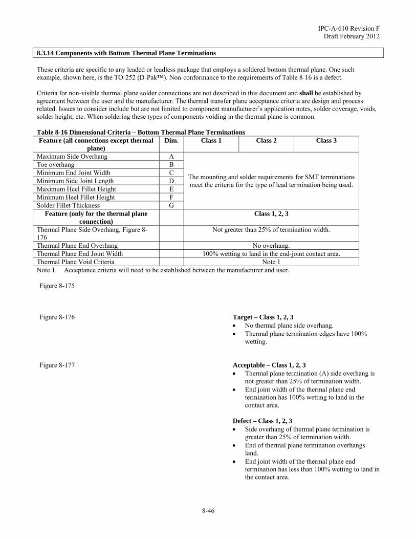
IPC-A-610 Revision F Draft February 2012
8-46
8.3.14 Components with Bottom Thermal Plane Terminations These criteria are specific to any leaded or leadless package that employs a soldered bottom thermal plane. One such example, shown here, is the TO-252 (D-Pak™). Non-conformance to the requirements of Table 8-16 is a defect. Criteria for non-visible thermal plane solder connections are not described in this document and shall be established by agreement between the user and the manufacturer. The thermal transfer plane acceptance criteria are design and process related. Issues to consider include but are not limited to component manufacturer’s application notes, solder coverage, voids, solder height, etc. When soldering these types of components voiding in the thermal plane is common. Table 8-16 Dimensional Criteria – Bottom Thermal Plane Terminations Feature (all connections except thermal
plane) Dim. Class 1 Class 2 Class 3
Maximum Side Overhang A
The mounting and solder requirements for SMT terminations meet the criteria for the type of lead termination being used.
Toe overhang B Minimum End Joint Width C Minimum Side Joint Length D Maximum Heel Fillet Height E Minimum Heel Fillet Height F Solder Fillet Thickness G
Feature (only for the thermal plane connection)
Class 1, 2, 3
Thermal Plane Side Overhang, Figure 8-176
Not greater than 25% of termination width.
Thermal Plane End Overhang No overhang. Thermal Plane End Joint Width 100% wetting to land in the end-joint contact area. Thermal Plane Void Criteria Note 1 Note 1. Acceptance criteria will need to be established between the manufacturer and user.
Target – Class 1, 2, 3 No thermal plane side overhang. Thermal plane termination edges have 100%
wetting. Acceptable – Class 1, 2, 3 Thermal plane termination (A) side overhang is
not greater than 25% of termination width. End joint width of the thermal plane end
termination has 100% wetting to land in the contact area.
Defect – Class 1, 2, 3 Side overhang of thermal plane termination is
greater than 25% of termination width. End of thermal plane termination overhangs
land. End joint width of the thermal plane end
termination has less than 100% wetting to land in the contact area.
Figure 8-175
Figure 8-176
Figure 8-177

IPC-A-610 Revision F Draft February 2012
8-47
8.3.15 Flattened Post Connections This termination style is sometimes referred to as nail-head pin. Criteria have not been established for Class 3 for this termination style. Process development and control is essential for continued success of assembly methods and implementation of materials. Non-conformance to the requirements of Table 8-17 is a defect. Table 8-17 Dimensional Criteria Flattened Post Connections
Feature Class1 Class 2 Class 3 Maximum Termination Overhang, Square Solder Land
75% Termination Width (W), Notes 1,
2
50% Termination Width (W), Notes 1,
2 Criteria not established
Maximum Termination Overhang, Round Solder Land
50% Termination Width (W), Notes 1,
2
25% Termination Width (W), Notes 1,
2 Maximum Fillet Height Note 4 Minimum Fillet Height Note 3 Note 1 Do not violate minimum electrical clearance. Note 2 Lead diameter is less than diameter or side length of the solder land. Note 3 Wetting is evident. Note 4 Solder does not touch package body. 8.3.15.1 Flattened Post Connections, Maximum Termination Overhang – Square Solder Land
Target Class 1, 2 No overhang. Acceptable Class 1 Overhang less than 75%. Acceptable Class 2 Overhang less than 50%. Defect Class 1 Overhang exceeds 75%. Defect Class 2 Overhang exceeds 50%.
8.3.15.2 Flattened Post Connections, Maximum Termination Overhang – Round Solder Land
Target Class 1, 2 No overhang. Acceptable Class 1 Overhang less than 50%. Acceptable Class 2 Overhang less than 25%.
Figure 8-178
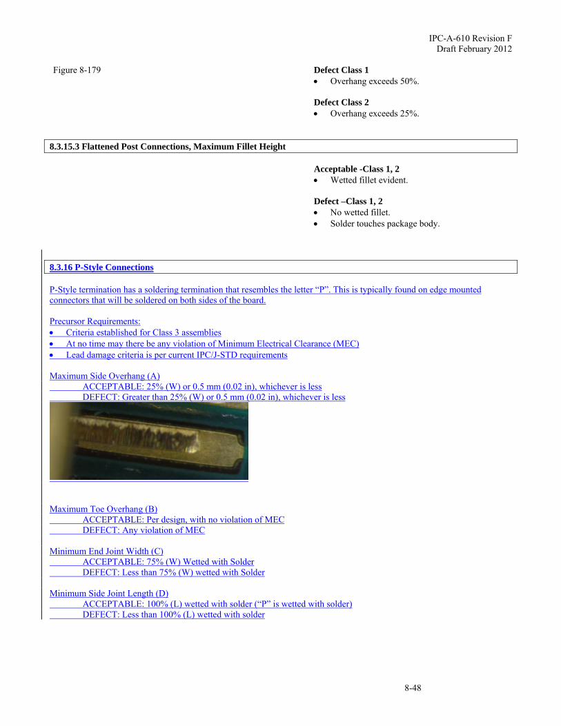
IPC-A-610 Revision F Draft February 2012
8-48
Defect Class 1 Overhang exceeds 50%. Defect Class 2 Overhang exceeds 25%.
8.3.15.3 Flattened Post Connections, Maximum Fillet Height
Acceptable -Class 1, 2 Wetted fillet evident. Defect –Class 1, 2 No wetted fillet. Solder touches package body.
8.3.16 P-Style Connections P-Style termination has a soldering termination that resembles the letter “P”. This is typically found on edge mounted connectors that will be soldered on both sides of the board. Precursor Requirements: Criteria established for Class 3 assemblies At no time may there be any violation of Minimum Electrical Clearance (MEC) Lead damage criteria is per current IPC/J-STD requirements Maximum Side Overhang (A) ACCEPTABLE: 25% (W) or 0.5 mm (0.02 in), whichever is less DEFECT: Greater than 25% (W) or 0.5 mm (0.02 in), whichever is less
Maximum Toe Overhang (B) ACCEPTABLE: Per design, with no violation of MEC DEFECT: Any violation of MEC Minimum End Joint Width (C) ACCEPTABLE: 75% (W) Wetted with Solder DEFECT: Less than 75% (W) wetted with Solder Minimum Side Joint Length (D) ACCEPTABLE: 100% (L) wetted with solder (“P” is wetted with solder) DEFECT: Less than 100% (L) wetted with solder
Figure 8-179
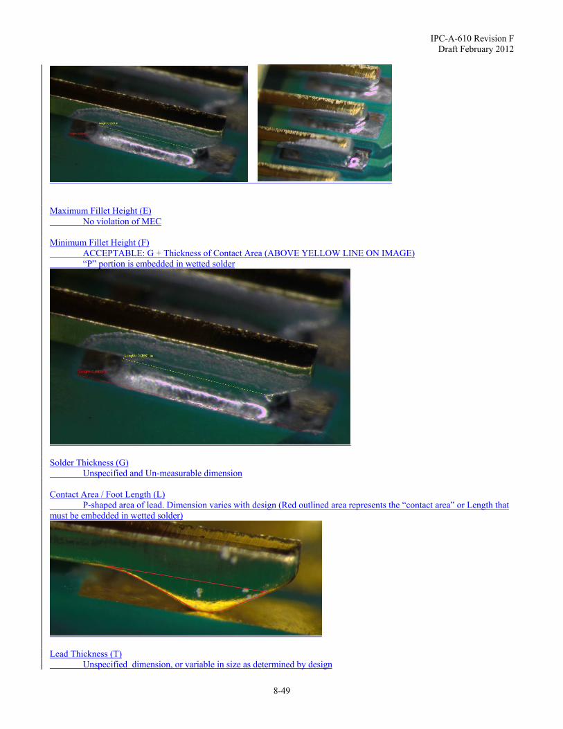
IPC-A-610 Revision F Draft February 2012
8-49
Maximum Fillet Height (E) No violation of MEC Minimum Fillet Height (F) ACCEPTABLE: G + Thickness of Contact Area (ABOVE YELLOW LINE ON IMAGE) “P” portion is embedded in wetted solder
Solder Thickness (G) Unspecified and Un-measurable dimension Contact Area / Foot Length (L) P-shaped area of lead. Dimension varies with design (Red outlined area represents the “contact area” or Length that must be embedded in wetted solder)
Lead Thickness (T) Unspecified dimension, or variable in size as determined by design

IPC-A-610 Revision F Draft February 2012
8-50
Lead Width (W) Unspecified dimension, or variable in size as determined by design 8.3.17 NEW—VARIATION OF BUTT CONNECTION
The bump on the bottom assures a fillet across most of the bottom; the attached solder slug controls the amount of solder; the two holes in the lead assure a strong solder fillet. A technical paper with extensive test data was presented and is available from IPC.
8.4 Specialized SMT Terminations The IPC committee that maintains this standard has received requests to include a number of specialized SMT termination styles such as shown in Figures 8-180, 8-181 and 8-182. Often these termination styles are unique to a particular component or are specially made for a limited number of users. Before acceptance criteria can be developed there needs to be significant use so that a history of failure data can be captured from multiple users. Clause 1.4.1.7 of this standard is repeated here.
1.4.1.7 Specialized Designs IPC-A-610, as an industry consensus document, cannot address all of the possible components and product design combinations. Where uncommon or specialized technologies are used, it may be necessary to develop unique acceptance criteria. However, where similar characteristics exist, this document may provide guidance for product acceptance criteria. Often, unique definition is necessary to consider the specialized characteristics while considering product performance criteria. The development should include customer involvement or consent and for Class 3 the criteria shall include agreed definition of product acceptance. Whenever possible these criteria should be submitted to the IPC Technical Committee to be considered for inclusion in upcoming revisions of this standard.
8.5 Surface Mount Connectors
Figure 8-180 Figure 8-181 Figure 8-182
IPC-A-610 Revision F Draft February 2012
8-51
These criteria apply to soldered connectors. For connector damage criteria see 9.5. The mounting and solder requirements for SMT connectors shall meet the criteria for the type of lead termination being used. There are no illustrations for these criteria.
Target - Class 1, 2, 3 Connector is flush with board. Acceptable - Class 1, 2, 3 Back edge of connector is flush; entering edge of
connector does not violate component height. Board lock is fully inserted/snapped through the
board. Any tilt, provided:
Maximum height requirements are not exceeded. Mates correctly.

IPC-A-610 Revision F Draft February 2012
8-52
Defect - Class 1, 2, 3 Will not mate when used in application due to angle. Component violates height requirements. Boardlock is not fully inserted/snapped into board. Note: Connectors need to meet form, fit and function requirements. A trial mating of connector to connector or to assembly may be required for final acceptance.
8.6 Jumper Wires These criteria do not constitute authority for repair to assemblies without prior customer consent; see 1.1. This section establishes visual acceptability criteria for the installation of discrete wires (jumper wires, haywires, etc.) used to interconnect components where there is no continuous printed circuit. The requirements relative to wire type, wire routing, staking and soldering requirements are the same for both haywires and jumper wires. For the sake of simplicity only the more common term, jumper wires, is used in this section; however these requirements would apply to both haywires and jumper wires. Information concerning rework and repair can be found in IPC-7711/7721. The following items are addressed: Wire selection; see 7.5.1. Wire routing; see 7.5.2. Adhesive staking of wire, see 7.5.3. Solder termination, see 7.5.4 for through-hole jumper wire criteria, and 8.6.1 for SMT jumper wire criteria. They may be terminated in plated holes, and/or to terminal standoffs, conductor lands, and component leads. Jumper wires are considered as components and are covered by an engineering instruction document for routing, termination, staking and wire type. Keep jumper wires as short as practical and unless otherwise documented do not route over or under other replaceable components. Design constraints such as real estate availability and minimum electrical clearance need to be taken into consideration when routing or staking wires. A jumper wire 25 mm [0.984 in] maximum in length whose path does not pass over conductive areas and do not violate the designed spacing requirements may be uninsulated. Insulation, when required on the jumper wires, shall be compatible with conformal coating when conformal coating is required. 8.6.1 Jumper Wires – SMT There is no adhesive on component bodies, leads or lands. Adhesive deposits do not obscure or interfere with solder connections. For all lap solder connections described in this section the following conditions are acceptable: Insulation clearance does not permit shorting to noncommon conductors or violate minimum electrical clearance. Evidence of wetting of jumper wire and lead or the land. Wire contour or end is discernible in the solder connection. No fractures in solder connection. Wire overhang does not violate minimum electrical clearance. Note: For applications of high frequency, i.e., RF, leads extending above the knee of the component could present problems.
IPC-A-610 Revision F Draft February 2012
8-53
8.6.1.1 Jumper Wires - SMT - Chip and Cylindrical End Cap Components
Target - Class 1, 2, 3 Lead is positioned parallel to longest dimension
of the land. Solder fillet length equal to land width (P). Acceptable - Class 1,2,3 Wire to component termination-land solder
connection length is at least 50% of land width (P) or twice the conductor diameter, whichever is greater.
Defect - Class 1,2,3 Wire to component termination-land solder
connection length is less than 50% of land width (P) or twice the conductor diameter, whichever is greater.
Wire soldered on top of chip component termination.
8.6.1.2 Jumper Wires - SMT - Gull Wing These criteria are applicable to jumpers attached to leads. See 8.6.1.5 for jumpers attached to lands.
Acceptable - Class 1,2,3 Wire length and solder wetting are equal to or
greater than 75% from edge of land to knee of lead (L).
The wire end does not extend past the lead knee bend.
Wire does not violate minimum electrical clearance.
Defect - Class 1,2,3 Wire length and solder wetting is less than 75%
from edge of land to knee of lead (L). Wire end extends past knee of bend. Wire violates minimum electrical clearance.
Figure 8-183
Figure 8-184
Figure 8-185
Figure 8-186
Figure 8-187

IPC-A-610 Revision F Draft February 2012
8-54
8.6.1.3 Jumper Wires - SMT - J Lead These criteria are applicable to jumpers attached to leads. See 8.6.1.5 for jumpers attached to lands.
Target - Class 1, 2, 3 Wire to lead-land interface solder connection is
equal to (L). Acceptable - Class 1,2,3 Wire length and solder wetting is equal to or
more than 75% height of the J-lead (L). The wire end does not extend past the knee of
the component lead. Defect - Class 1,2,3 Wire length and solder wetting is less than 75%
height of the J-lead (L). The wire end extends past the knee of the
component lead. Wire violates minimum electrical clearance.
8.6.1.4 Jumper Wires - SMT – Castellations These criteria are applicable to jumpers attached to castellations. See 8.6.1.5 for jumpers attached to lands.
Acceptable - Class 1,2,3 Wire length and solder wetting is at least 75%
top of land to top of castellation. Wire is placed against the back of the
castellation. Wire does not extend above the top of the
castellation. Defect - Class 1,2,3 Wire length and solder wetting is less than 75%
top of land to top of castellation. Wire end extends past top of castellation. Wire violates minimum electrical clearance.
Figure 8-188
Figure 8-189

IPC-A-610 Revision F Draft February 2012
8-55
8.6.1.5 Jumper Wires - SMT - Land These criteria are applicable to vacant lands or lands with leads attached.
Target - Class 1, 2, 3 Lead is positioned parallel to longest dimension
of the land. Lead length and solder fillet equal to (P). <HIGHLIGHTED CRITERIA FROM DEBBIE WADE, ART, Sep2011 ACTION ITEM PROPOSAL> Acceptable - Class 1,2,3 For a land width (P) that is 6 mm (0.236 in) or
larger, the wire to lead-land interface is at least 2 wire diameters.
For a land width (P) less than 6 mm (0.236 in), the wire to lead-land interface is at least 50% of the land width or 2 wire diameter whichever is greater.
Wire length and solder wetting are equal to or greater than 75% from edge of land to knee of lead (L).
Wire end does not extend past the knee of the lead.
Wire is lap soldered to a PTH/Via surface. (committee to decide on lap length. Do you want me to use the same 75% wording?)
Acceptable solder connection at wire and solder interface.
Wire discernible in solder connection. Wire does not violate minimum electrical
clearance.
Figure 8-190
IPC-A-610 Revision F Draft February 2012
8-56
Defect - Class 1,2,3 For a land width (P) that is 6 mm (0.236 in) or
larger, the wire to lead-land interface is less than 2 wire diameter.
For a land width (P) less than 6 mm (0.236 in), the wire to lead-land interface is less than 50% of the land width or 2 wire diameter whichever is greater.
Wire violates minimum electrical clearance. Wire length and solder wetting are less than 75%
from the edge of the land to the knee of the lead(L).
Wire end extends past the knee of the lead. (Do you want be to add wording for insufficient
lap position and solder wetting for land/Via?). Wire is not discernible in the solder connection. Wire violates minimum electrical clearance.

IPC-A-610 Revision F Draft February 2012
9-1 Illustrations and text are copyright IPC and may be copied only for use in licensed translation of IPC-A-610 Revision F.
9 Component Damage The following topics are addressed in this section: 9.1 Loss of Metallization 9.2 Chip Resistor Element 9.3 Leaded/Leadless Devices 9.4 Ceramic Chip Capacitors 9.5 Connectors 9.6 Relays 9.7 Transformer Core Damage 9.8 Connectors, Handles, Extractors, Latches 9.9 Edge Connector Pins 9.10 Press Fit Pins 9.11 Backplane Connector Pins 9.12 Heat Sink Hardware
IPC-A-610 Revision F Draft February 2012
9-2 Illustrations and text are copyright IPC and may be copied only for use in licensed translation of IPC-A-610 Revision F.
9.1 Loss of Metallization
Acceptable - Class 1, 2, 3 Metallization loss on any termination side (not
the end face) of a five-sided termination component, up to 25% of the component width (W) or the component thickness (T).
Maximum of 50% of metallization loss of top metallization area (for each terminal end) of a three-sided termination component, Figures 9-1, 2.
Defect - Class 1, 2, 3 Metallization loss on the terminal end face
exposing the ceramic, Figure 9-3(1). Metallization loss on any termination side (not
the end face) on a five-sided termination component greater than 25% of component width (W) or component thickness (T), Figures 9-4 and 9-5.
Metallization loss greater than 50% of the top area on a three-sided termination component, Figures 9-5 and 9-6.
Irregular shapes exceeding maximum or minimum dimensions for that component type.
9.2 Chip Resistor Element
Acceptable - Class 1, 2, 3 For chip resistors, any chip-out (nick) of the top
surface (adhesive coating) of 1206 and larger component is less than 0.25 mm [0.00984 in] from the edge of the component.
No damage to the resistive element in area B. Defect - Class 1,2,3 Any chip-outs in resistive elements.
Figure 9-1 1. Metallization missing 2. Adhesive coating 3. Resistive element 4. Substrate (ceramic/alumina 5. Terminal end Figure 9-2
Figure 9-3 Figure 9-4 Figure 9-5 Figure 9-6
Figure 9-7
Figure 9-8

IPC-A-610 Revision F Draft February 2012
9-3 Illustrations and text are copyright IPC and may be copied only for use in licensed translation of IPC-A-610 Revision F.
9.3 Leaded/Leadless Devices These criteria are applicable to leaded and leadless devices.
Target - Class 1, 2, 3 Finish not damaged. Component bodies are free of scratches, cracks,
chips, and crazing. ID markings are legible. Acceptable - Class 1, 2, 3 Chips or scratches that do not expose the component
substrate or active element, or affect structural integrity, form, fit, or function.
Chips or cracks in component meniscus that do not expose the component substrate or active element, or affect structural integrity, form, fit, or function.
Structural integrity is not compromised. No evidence of cracks or damage to the lid or lead
seals of a component. Dents, scratches do not affect form, fit & function
and do not exceed manufacturer’s specifications. No burned, charred components. Acceptable - Class 1 Process Indicator - Class 2, 3 Indentations or chipouts on plastic body components
do not enter lead seal or lid seals or expose an internal functional element, Figures 9-12, 13, 14.
Component damage has not removed required identification.
Component insulation/sleeving has damage provided that: Damaged area shows no evidence of increasing,
e.g. rounded edges of the damage with no cracks, sharp corners, brittle material from heat damage, etc., Figures 9-13, 14.
Exposed component conductive surface provides no danger of shorting to adjacent components or circuitry, Figure 9-15.
Figure 9-9
Figure 9-10
Figure 9-11 1. Chip 2. Crack
Figure 9-12 Figure 9-13 Figure 9-14 Figure 9-15

IPC-A-610 Revision F Draft February 2012
9-4 Illustrations and text are copyright IPC and may be copied only for use in licensed translation of IPC-A-610 Revision
F.
Defect - Class 1, 2, 3 Chip out or crack that enters into the seal, Figure 9-
16. There are cracks leading from the chipout on a
ceramic body component, Figure 9-16. Chip or crack that exposes the component substrate
or active element, or affects hermeticity, integrity, form, fit, or function; Figures 9-17, 18, 19, 20. Chips or cracks in glass body, Figures 9-21, 22.
Cracked or damaged glass bead beyond part specification (not shown).
Required identification is missing due to component damage, Figure 9-23.
The insulating coating is damaged to the extent that the internal functional element is exposed or the component shape is deformed (not shown).
Damaged area shows evidence of increasing, for instance from cracks, sharp corners, brittle material from heat, etc., Figure 9-24.
Damage permits potential shorting to adjacent components or circuitry.
Flaking, peeling, or blistering of plating. Burned, charred components (the charred surface on
a component has black, dark brown appearance due to excessive heat), Figure 9-25.
Dents, scratches in the component body that affect form, fit & function or exceed component manufacturer’s specifications (not shown).
Cracks in shield material, Figure 9-26.
9.4 Ceramic Chip Capacitors
Target - Class 1, 2, 3 No nicks, cracks, or stress fractures. Acceptable - Class 1, 2 Nicks or chip-outs not greater than dimensions stated
in Table 9-1, each considered separately. Table 9-1 Chip-Out Criteria
(T) 25% of the thickness (W) 25% of the width (L) 50% of the length
Acceptable - Class 1, 2, 3 Component color change due to thermal exposure in
the reflow process.
Figure 9-16 1. Chip enters seal 2. Exposed lead 3. Seal
Figure 9-17
Figure 9-18 Figure 9-19
Figure 9-20 Figure 9-21 Figure 9-22 1. Cracked insulator Figure 9-23 Figure 9-24 Figure 9-25 Figure 9-26
Figure 9-27
Figure 9-28

IPC-A-610 Revision F Draft February 2012
9-5 Illustrations and text are copyright IPC and may be copied only for use in licensed translation of IPC-A-610 Revision
F.
Defect - Class 1, 2, 3 Any nick or chip-out in the termination area, or
exposing an electrode. Any cracks or stress fractures. Damage in excess of Table 9-1.
9.5 Connectors These criteria cover the plastic molded housings/shrouds which are used primarily as a guide for the mating connector. Connector pins are typically held by interference fit in a housing. Visual inspection of housings and shrouds includes physical damage such as cracks and deformation.
Target – Class 1, 2, 3 No discernable physical damage. No burrs on housing/shroud. No cracks in housing/shroud. Connector/header pins are straight. Acceptable - Class 1, 2, 3 Burrs on housing but still attached (have not broken
loose) and do not affect form, fit or function. Cracks in noncritical areas (do not impact integrity of
the housing/shroud). Minor scratches, chips, or thermal deformation that
do not compromise protection of the contacts or interfere with proper mating.
Pins are bent off center by 25% pin thickness/diameter or less.
Defect – Class 1, 2, 3 Burrs, cracks or other deformations that impact the
mechanical integrity or functionality of the housing. Pins are bent off center by more than 25% pin
thickness/diameter. Acceptable - Class 1, 2, 3 No evidence of burn or char. Minor chips, scrapes, scratches or melting that does
not affect form, fit or function. Process Indicator - Class 2, 3 Slight discoloration.
Figure 9-29
Figure 9-30 Figure 9-31 Figure 9-32 Figure 9-33
Figure 9-34
Figure 9-35 Figure 9-36
Figure 9-37
IPC-A-610 Revision F Draft February 2012
9-6 Illustrations and text are copyright IPC and may be copied only for use in licensed translation of IPC-A-610 Revision
F.
Defect - Class 1, 2, 3 Evidence of burning or charring. Changes in shape, chips, scrapes, scratches, melting
or other damage that affect form, fit or function.
9.6 Relays
Acceptable – Class 1, 2, 3 Minor scratches, cuts, chips, or other imperfections that
do not penetrate the case or affect the seal (not shown). Defect – Class 1, 2, 3 Scratches, cuts, chips, or other imperfections that
penetrate the case or affect the seal. The case is bulging or swollen.
9.7 Transformer Core Damage
Acceptable – Class 1, 2, 3 Chips and/or scratches on exterior edges of core
are permissible, providing they do not extend into core mating surfaces and do not exceed 1/2 the thickness of the core.
Defect – Class 1, 2, 3 Chip in the core material is located on mating
surface (arrow). Chip extending greater than 50% of the core
thickness. Cracks in the core material.
9.8 Connectors, Handles, Extractors, Latches This section shows some of the many different types of hardware mounted devices, e.g. connectors, handles, extractors and plastic molded parts.
Target - Class 1, 2, 3 No damage to part, printed board or securing
hardware (rivets, screws, etc.).
Figure 9-38
Figure 9-39
Figure 9-40
Figure 9-41
Figure 9-42
Figure 9-43 1. Extractor 2. Securing hardware 3. Component lead

IPC-A-610 Revision F Draft February 2012
9-7 Illustrations and text are copyright IPC and may be
copied only for use in licensed translation of IPC-A-610 Revision F.
Acceptable - Class 1 Cracks in the mounted part extend no more than
50% of the distance between a mounting hole and a formed edge.
Defect - Class 1 Cracks in the mounted part extend more than 50%
of the distance between a mounting hole and a formed edge.
Defect - Class 2, 3 Cracks in mounted part. Defect - Class 1, 2, 3 Crack connects a mounting hole to an edge. Damage/stress to connector lead pins.
9.9 Edge Connector Pins
Acceptable - Class 1, 2, 3 Contact is not broken or twisted. Defect - Class 1, 2, 3 Contacts are twisted or otherwise deformed (A). Contact is broken (B).
9.10 Press Fit Pins
Defect - Class 1, 2, 3 Damaged pin as a result of handling or insertion.
Twisted. Mushroomed. Bent. Exposed basis metal. Burr.
Figure 9-44 1. Crack
Figure 9-45
Figure 9-46 Figure 9-47 Figure 9-48 1. Burr 2. Plating missing
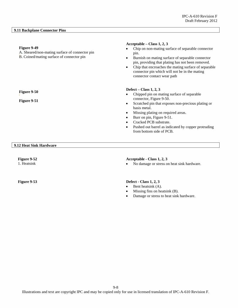
IPC-A-610 Revision F Draft February 2012
9-8 Illustrations and text are copyright IPC and may be copied only for use in licensed translation of IPC-A-610 Revision F.
9.11 Backplane Connector Pins
Acceptable – Class 1, 2, 3 Chip on non-mating surface of separable connector
pin. Burnish on mating surface of separable connector
pin, providing that plating has not been removed. Chip that encroaches the mating surface of separable
connector pin which will not be in the mating connector contact wear path
Defect – Class 1, 2, 3 Chipped pin on mating surface of separable
connector, Figure 9-50. Scratched pin that exposes non-precious plating or
basis metal. Missing plating on required areas. Burr on pin, Figure 9-51. Cracked PCB substrate. Pushed out barrel as indicated by copper protruding
from bottom side of PCB.
9.12 Heat Sink Hardware
Acceptable - Class 1, 2, 3 No damage or stress on heat sink hardware. Defect - Class 1, 2, 3 Bent heatsink (A). Missing fins on heatsink (B). Damage or stress to heat sink hardware.
Figure 9-49 A. Sheared/non-mating surface of connector pin B. Coined/mating surface of connector pin
Figure 9-50 Figure 9-51
Figure 9-52 1. Heatsink
Figure 9-53
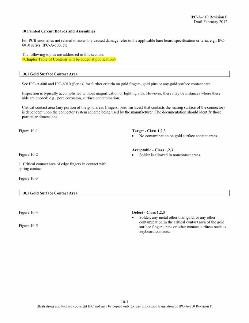
IPC-A-610 Revision F Draft February 2012
10-1 Illustrations and text are copyright IPC and may be copied only for use in licensed translation of IPC-A-610 Revision F.
10 Printed Circuit Boards and Assemblies For PCB anomalies not related to assembly caused damage refer to the applicable bare board specification criteria, e.g., IPC-6010 series, IPC-A-600, etc. The following topics are addressed in this section: <Chapter Table of Contents will be added at publication> 10.1 Gold Surface Contact Area See IPC-A-600 and IPC-6010 (Series) for further criteria on gold fingers, gold pins or any gold surface contact area. Inspection is typically accomplished without magnification or lighting aids. However, there may be instances where these aids are needed; e.g., pore corrosion, surface contamination. Critical contact area (any portion of the gold areas (fingers, pins, surfaces) that contacts the mating surface of the connector) is dependent upon the connector system scheme being used by the manufacturer. The documentation should identify those particular dimensions.
Target - Class 1,2,3 No contamination on gold surface contact areas. Acceptable - Class 1,2,3 Solder is allowed in noncontact areas.
10.1 Gold Surface Contact Area
Defect - Class 1,2,3 Solder, any metal other than gold, or any other
contamination in the critical contact area of the gold surface fingers, pins or other contact surfaces such as keyboard contacts.
Figure 10-1
Figure 10-2
1. Critical contact area of edge fingers in contact with spring contact
Figure 10-3
Figure 10-4
Figure 10-5
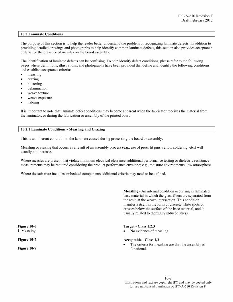
IPC-A-610 Revision F Draft February 2012
10-2 Illustrations and text are copyright IPC and may be copied only
for use in licensed translation of IPC-A-610 Revision F.
10.2 Laminate Conditions The purpose of this section is to help the reader better understand the problem of recognizing laminate defects. In addition to providing detailed drawings and photographs to help identify common laminate defects, this section also provides acceptance criteria for the presence of measles on the board assembly. The identification of laminate defects can be confusing. To help identify defect conditions, please refer to the following pages where definitions, illustrations, and photographs have been provided that define and identify the following conditions and establish acceptance criteria: measling crazing blistering delamination weave texture weave exposure haloing It is important to note that laminate defect conditions may become apparent when the fabricator receives the material from the laminator, or during the fabrication or assembly of the printed board. 10.2.1 Laminate Conditions - Measling and Crazing This is an inherent condition in the laminate caused during processing the board or assembly. Measling or crazing that occurs as a result of an assembly process (e.g., use of press fit pins, reflow soldering, etc.) will usually not increase. Where measles are present that violate minimum electrical clearance, additional performance testing or dielectric resistance measurements may be required considering the product performance envelope; e.g., moisture environments, low atmosphere. Where the substrate includes embedded components additional criteria may need to be defined.
Measling - An internal condition occurring in laminated base material in which the glass fibers are separated from the resin at the weave intersection. This condition manifests itself in the form of discrete white spots or crosses below the surface of the base material, and is usually related to thermally induced stress. Target - Class 1,2,3 No evidence of measling. Acceptable - Class 1,2 The criteria for measling are that the assembly is
functional.
Figure 10-6 1. Measling Figure 10-7 Figure 10-8
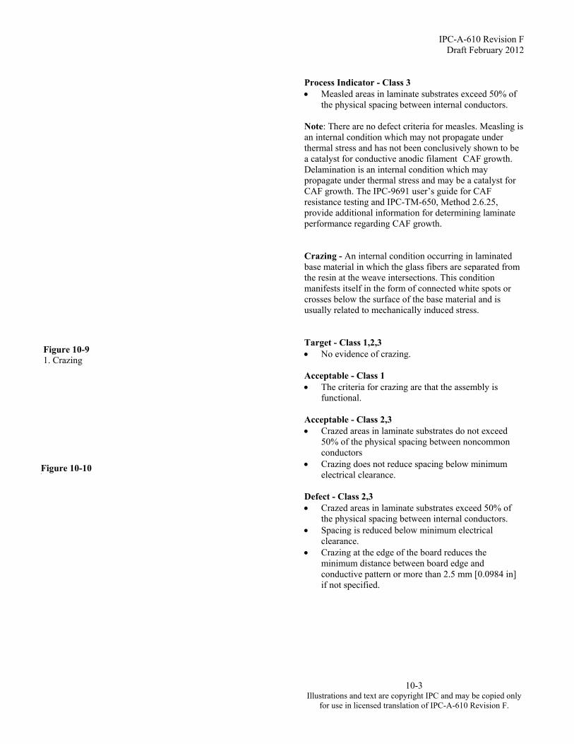
IPC-A-610 Revision F Draft February 2012
10-3 Illustrations and text are copyright IPC and may be copied only
for use in licensed translation of IPC-A-610 Revision F.
Process Indicator - Class 3 Measled areas in laminate substrates exceed 50% of
the physical spacing between internal conductors. Note: There are no defect criteria for measles. Measling is an internal condition which may not propagate under thermal stress and has not been conclusively shown to be a catalyst for conductive anodic filament CAF growth. Delamination is an internal condition which may propagate under thermal stress and may be a catalyst for CAF growth. The IPC-9691 user’s guide for CAF resistance testing and IPC-TM-650, Method 2.6.25, provide additional information for determining laminate performance regarding CAF growth. Crazing - An internal condition occurring in laminated base material in which the glass fibers are separated from the resin at the weave intersections. This condition manifests itself in the form of connected white spots or crosses below the surface of the base material and is usually related to mechanically induced stress. Target - Class 1,2,3 No evidence of crazing. Acceptable - Class 1 The criteria for crazing are that the assembly is
functional. Acceptable - Class 2,3 Crazed areas in laminate substrates do not exceed
50% of the physical spacing between noncommon conductors
Crazing does not reduce spacing below minimum electrical clearance.
Defect - Class 2,3 Crazed areas in laminate substrates exceed 50% of
the physical spacing between internal conductors. Spacing is reduced below minimum electrical
clearance. Crazing at the edge of the board reduces the
minimum distance between board edge and conductive pattern or more than 2.5 mm [0.0984 in] if not specified.
Figure 10-9 1. Crazing
Figure 10-10
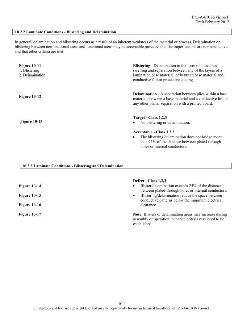
IPC-A-610 Revision F Draft February 2012
10-4 Illustrations and text are copyright IPC and may be copied only for use in licensed translation of IPC-A-610 Revision F.
10.2.2 Laminate Conditions - Blistering and Delamination In general, delamination and blistering occurs as a result of an inherent weakness of the material or process. Delamination or blistering between nonfunctional areas and functional areas may be acceptable provided that the imperfections are nonconductive and that other criteria are met.
Blistering - Delamination in the form of a localized swelling and separation between any of the layers of a lamination base material, or between base material and conductive foil or protective coating. Delamination - A separation between plies within a base material, between a base material and a conductive foil or any other planar separation with a printed board. Target - Class 1,2,3 No blistering or delamination. Acceptable - Class 1,2,3 The blistering/delamination does not bridge more
than 25% of the distance between plated-through holes or internal conductors.
10.2.2 Laminate Conditions - Blistering and Delamination
Defect - Class 1,2,3 Blister/delamination exceeds 25% of the distance
between plated-through holes or internal conductors. Blistering/delamination reduce the space between
conductive patterns below the minimum electrical clearance.
Note: Blisters or delamination areas may increase during assembly or operation. Separate criteria may need to be established.
Figure 10-11 1. Blistering 2. Delamination
Figure 10-12
Figure 10-13
Figure 10-14 Figure 10-15 Figure 10-16 Figure 10-17
IPC-A-610 Revision F Draft February 2012
10-5 Illustrations and text are copyright IPC and may be copied only for use in licensed translation of IPC-A-610 Revision F.
10.2.3 Laminate Conditions - Weave Texture/Weave Exposure
Weave Texture - A surface condition of base material in which a weave pattern of glass cloth is apparent although the unbroken fibers are completely covered with resin. Acceptable - Class 1,2,3 Weave texture is an acceptable condition in all
classes but is confused with weave exposure because of similar appearance.
Note: Microsection may be used as a reference for this condition. Weave Exposure - A surface condition of base material in which the unbroken fibers of woven glass cloth are not completely covered by resin. Target - Class 1,2,3 No weave exposure. Acceptable - Class 1,2,3 Weave exposure does not reduce the spacing between
conductive patterns below specification minimums. Acceptable – Class 1 Defect – Class 2,3 Surface damage that cuts into laminate fibers. Defect - Class 1,2,3 Weave exposure reduces the spacing between
conductive patterns to less than the minimum electrical clearance.
Figure 10-18
Figure 10-19
Figure 10-20
Figure 10-21
IPC-A-610 Revision F Draft February 2012
10-6 Illustrations and text are copyright IPC and may be copied only for use in licensed translation of IPC-A-610 Revision F.
10.2.4 Laminate Conditions - Haloing and Edge Delamination Haloing - A condition existing in the base material in the form of a light area around holes or other machined areas on or below the surface of the base material.
Target - Class 1,2,3 No haloing or edge delamination. No nicks/damage on smooth board edges. Acceptable - Class 1,2,3 Penetration of haloing or edge delamination does not
reduce edge spacing more than 50% of that specified by drawing note or equivalent documentation. If none is specified, the distance from haloing or edge delamination to conductors is greater than 0.127mm [0.005 in). The maximum haloing or edge delamination is not greater than 2.5mm [0.0984 in).
Board edges are rough but not frayed. Defect - Class 1,2,3
Penetration of haloing, edge delamination (Figure 10-28) or routing (Figure 10-29) that reduces edge spacing more than 50% of that specified by drawing note or equivalent documentation. If none is specified, the distance from haloing or edge delamination to conductors is ≥0.127mm [0.005 in]. The maximum haloing or edge delamination is greater than 2.5mm [0.0984 in).
Cracks in the laminate, see Figure 10-29 arrow.
10.2.5 Burns
Defect – Class 1,2,3 Burns that physically damage surface or the
assembly.
Figure 10-22
Figure 10-23 Figure 10-24
Figure 10-25 Figure 10-26 Figure 10-27 Figure 10-28 Figure 10-29
Figure 10-30 Figure 10-31 Figure 10-32
IPC-A-610 Revision F Draft February 2012
10-7 Illustrations and text are copyright IPC and may be copied only for use in licensed translation of IPC-A-610 Revision F.
10.2.6 Laminate Conditions - Bow and Twist
Figure 10-33 is an example of bow. Acceptable – Class 1,2,3 Bow and twist does not cause damage during post
solder assembly operations or end use. Consider “Form, Fit and Function” and product reliability.
Defect – Class 1,2,3 Bow and twists causes damage during post solder
assembly operations or end use or affects form, fit or function.
Note: Bow and twist after solder should not exceed 1.5% for through-hole and 0.75% for surface mount printed board applications (See IPC-TM-650, 2.4.22). It may be necessary to confirm through testing that bow and twist has not created stress that will result in solder connection fracture or component damage.
10.2.7 Laminate Conditions - Depanelization These criteria are applicable to PCAs with or without breakaway tabs. IPC-A-600 provides additional criteria for depanelization of bare boards.
Target – Class 1,2,3 Edges are smooth with no burrs, nicks or
haloing. Acceptable − Class 1,2,3 Edges are rough but not frayed. Nicks or routing do not exceed 50% of the
distance from the board edge to the nearest conductor or 2.5 mm [0.098 in], whichever is less. See 10.2.4 for haloing and 10.2.1 for crazing.
Edge conditions - loose burrs do not affect fit, form or function.
Defect − Class 1,2,3 Edges are frayed. Nicks or routing exceed 50% of the distance
from the board edge to the nearest conductor or 2.5 mm [0.098 in], whichever is less. See 10.2.4 for haloing and 10.2.1 for crazing.
Edge conditions - loose burrs affect fit, form or function.
Figure 10-33
Figure 10-34 1. Bow 2. Points A, B and C are touching base 3. Twist
Figure 10-35
Figure 10-36
Figure 10-37 Figure 10-38 Figure 10-39
Figure 10-40 Figure 10-41 Figure 10-42

IPC-A-610 Revision F Draft February 2012
10-8 Illustrations and text are copyright IPC and may be copied only for use in licensed translation of IPC-A-610 Revision F.
10.3 Conductors/Lands 10.3.1 Conductors/Lands – Reduction in Cross-Sectional Area These criteria are applicable to conductors and lands on rigid, flex and rigid-flex circuitry. IPC-6010 (Series) provides the requirements for conductor width and thickness reduction. Conductor Imperfections – The physical geometry of a conductor is defined by its width x thickness x length. Any combination of defects does not reduce the equivalent cross-sectional area (width x thickness) of the conductor by more than 20% of the minimum value (minimum thickness x minimum width) for Class 2 and 3, and 30% of the minimum value for Class 1. Conductor Width Reduction – Allowable reduction of the conductor width (specified or derived) due to isolated defects (i.e., edge roughness, nicks, pinholes and scratches) does not exceed 20% of the minimum printed conductor width for Class 2 and 3, and 30% of the minimum printed conductor width for Class 1.
Defect - Class 1
Reduction in minimum width of printed conductors by more than 30%.
Reduction in minimum printed conductor width or length of lands by more than 30%.
Defect - Class 2,3 Reduction in minimum width of printed conductors
by more than 20%. Reduction in width or length of lands by more than
20%. Note: Even small changes in cross-sectional area can have a large impact on impedance of RF circuitry. Alternate criteria may need to be developed.
10.3.2 Conductors/Lands – Lifted Pads/Lands Except as noted, these criteria are for lifted pads/lands with or without a lead in the via/PTH.
Target – Class 1,2,3 No separation between conductor or PTH land and
the laminate surface. Process Indicator – Class 1,2,3 Separation between outer edge of conductor or land
and laminate surface is less than one land thickness. Note: Lifted and/or separated land area(s) is typically a result of the soldering process that warrants immediate investigation to determine root cause. Efforts to eliminate and/or prevent this condition should be made.
Figure 10-43 1. Minimum Conductor Width Figure 10-44 Figure 10-45
Figure 10-46
Figure 10-47

IPC-A-610 Revision F Draft February 2012
10-9 Illustrations and text are copyright IPC and may be copied only
for use in licensed translation of IPC-A-610 Revision F.
Defect – Class 1,2,3 Separation between conductor or PTH land and
laminate surface is greater than one pad thickness. Defect – Class 3 Any lifting of a land if there is a unfilled via or via
with no lead in the land.
10.3.3 Conductors/Lands – Mechanical Damage
Defect – Class 1,2,3 Damage to functional conductors or lands that affects
form, fit or function.
10.4 Flexible and Rigid-Flex Printed Circuitry 10.4.1 Flexible and Rigid-Flex Printed Circuitry – Damage The trimmed edge of the flexible printed circuit or the flexible section rigid-flex printed circuit is free of burrs, nicks, delamination, or tears in excess of that allowed in the procurement documentation. The deformation of a stiffener board should conform to the master drawing or the individual specification. Note: For SMT or through-hole component mounting, placement, soldering, cleanliness criteria on flex assemblies, etc. follow the applicable sections of this standard.
Target – Class 1,2,3 Free of nicks, tears, burns, charring or melting.
Minimum edge to conductor spacing maintained. The trimmed edge of the flexible printed circuitry or
the flexible section of finished rigid-flex printed circuitry is free of burrs, nicks, delamination, and tears.
Figure 10-48
Figure 10-49 Figure 10-50
Figure 10-51 Figure 10-52 Figure 10-53
Figure 10-54 Figure 10-55
IPC-A-610 Revision F Draft February 2012
10-10 Illustrations and text are copyright IPC and may be copied only
for use in licensed translation of IPC-A-610 Revision F.
Acceptable - Class 1,2,3
No nicks or tears in excess of that specified in the procurement documentation.
Edge to conductor spacing of the flexible portion is within requirements specified on the procurement documentation.
Nicks or haloing along the edges of the flexible printed circuitry, cutouts, and unsupported holes, providing the penetration does not exceed 50% of the distance from the edge to the nearest conductor or 2.5 mm [0.0984 in], whichever is less.
The area of blister or delamination between flex circuitry and a stiffener board does not exceed 20% of the joined area provided the thickness of the blister does not exceed the thickness limit of the entire board.
Defect – Class 1,2,3 Nicks, tears, haloing or imperfections more than 50%
of the distance from the edge to the nearest conductor or 2.5 mm [0. 098 in], whichever is less, or in excess of that specified in the procurement documentation.
Edge to conductor spacing does not comply with specified requirements.
The area of blister or delamination between flex circuitry and a stiffener board exceeds 20% of the joined area.
Evidence of burns, charring or melting of the insulation.
Note: Mechanically created indentions caused by contact between the coverlayer of flexible printed circuit boards or assemblies and molten solder are not rejectable. Additionally, care should be taken to avoid bending or flexing conductors during inspection.
10.4.2 Flexible and Rigid-Flex Printed Circuitry –Delamination Sometimes delamination takes place in the flex circuitry or between flex circuitry and the edge of a stiffener board during reflow, cleaning steps, etc. of assembly process.
Acceptable – Class 1,2,3 The distance from stiffener board edge in the straight
section is 0.5mm [0.0197 in] or less. The distance from stiffener board edge in the bend
section is 0.3mm or less. Delamination (separation) or bubbles do not bridge
conductors in the cover layers of the flexible circuitry.
Figure 10-56
Figure 10-57 Figure 10-58 Figure 10-59 Figure 10-60

IPC-A-610 Revision F Draft February 2012
10-11 Illustrations and text are copyright IPC and may be copied only
for use in licensed translation of IPC-A-610 Revision F.
Defect – Class 1,2,3 The distance from stiffener board edge in the straight
section exceeds 0.5mm [0.0197 in]. The distance from stiffener board edge in the bend
section exceeds 0.3mm [0.012 in]. Delamination (separation) or bubbles bridges
conductors in the cover layers of the flexible circuitry.
10.4.3 Flexible and Rigid-Flex Printed Circuitry – Discoloration There are no illustrations for these criteria.
Acceptable – Class 1,2,3 A discolored conductor meets the requirements of
dielectric withstanding voltage, flexural fatigue resistance, bending resistance, and solder temperature resistance, after being subjected to the moisture resistance test of 40°C, 40% relative humidity, 96 hours.
Acceptable – Class 1 Minimum discoloration. Defect – Class 1,2,3 A discolored conductor does not meet the
requirements of dielectric withstanding voltage, flexural fatigue resistance, bending resistance, or solder temperature resistance, after being subjected to the moisture resistance test of 40°C, 40% relative humidity, 96 hours.
10.4.4 Flexible and Rigid-Flex Printed Circuitry – Solder Wicking
Target – Class 1,2,3 Solder or plating on land covers all exposed metal
and stops at coverlayer. Acceptable – Class 1,2,3 Solder wicking or plating migration does not extend
into the bend or flex transition area. Acceptable – Class 2 Solder wicking/plating migration does not extend
under coverlayer more than 0.5 mm [0.020 in]. Acceptable – Class 3 Solder wicking/plating migration does not extend
under coverlayer more than 0.3 mm [0.012 in].
Figure 10-61
Figure 10-62
IPC-A-610 Revision F Draft February 2012
10-12 Illustrations and text are copyright IPC and may be copied only
for use in licensed translation of IPC-A-610 Revision F.
Defect – Class 2 Solder wicking/plating migration extends under
coverlayer more than 0.5 mm [0.020 in]. Defect – Class 3 Solder wicking/plating migration extends under
coverlayer more than 0.3 mm [0.012 in]. Defect - Class 1,2,3 Solder wicking or plating migration extends into the
bend or flex transition area. Spacing as a result of solder wicking or plating
migration violate minimum electrical clearance.
10.4.5 Flexible and Rigid-Flex Printed Circuitry – Attachment These criteria are applicable to the solder attachment of flex on PCB (FOB). When sufficient data has been collected this will be expanded to include flex on flex (FOF) and connection using anisotropically conductive flex (ACF).
Target – Class 1,2,3 No side overhang. Plated through holes in the connection areas are
filled 100%. Solder is fully wetted in edge semicircular plated
holes. Acceptable – Class 1,2,3 Side overhang of flex termination is equal to or
less than 20% of flex termination width. Plated through holes in the connection areas are
filled 50% or more. Wetted solder is visible in the edge semicircular
plated holes. Process Indicator – Class 1,2,3 No evidence of wetted solder in two adjacent
edge semicircular plated holes. Defect – Class 1,2,3 Side overhang of flex termination is more than
20% of flex termination width. Plated through holes in the connection areas are
less than 50% filled. No evidence of wetted solder in three or more
adjacent edge semicircular plated holes.
Figure 10-63
Figure 10-64 Figure 10-65
Figure 10-66
Figure 10-67

IPC-A-610 Revision F Draft February 2012
10-13 Illustrations and text are copyright IPC and may be copied only for use in licensed translation of IPC-A-610 Revision F.
10.5 Marking Marking Acceptability Requirements This section covers acceptability criteria for marking of printed boards and other electronic assemblies. Marking provides both product identification and traceability. It aids in assembly, in-process control, and field servicing. The methods and materials used in marking shall serve the intended purposes and shall be readable, durable, and compatible with the manufacturing processes and should remain legible through the life of the product. Examples of the markings addressed by this section include the following: a. Electronic Assemblies:
company logo board fabrication part numbers and revision level assembly part number, group number, and revision level component legends including reference designators and polarity indicators (only applies prior to assembly
processing/cleaning) certain inspection and test traceability indicators U.S. and other relevant regulatory agencies/certifications unique individual serial number date code
b. Modules and/or Higher Level Assemblies:
company logo product identification numbers, e.g., drawing number, revision and serial number installation and user information relevant regulatory agencies' certification labels
The fabrication and assembly drawings are the controlling documents for the locations and types of markings. Marking criteria specified in the drawings will take precedence over these criteria. In general, additive markings over metal surfaces are not recommended. Markings which serve as aids to assembly and inspection need not be visible after the components are mounted. Assembly marking (part numbers, serial numbers) need to remain legible (capable of being read and understood as defined by the requirements of this standard) after all tests, cleaning and other processes to which the item is subjected. Component markings, reference designators and polarity indicators should be legible and components should be mounted in such a manner that markings are visible. However, unless otherwise required, it is an acceptable condition if these markings are removed or damaged during normal cleaning or processing. Markings are not deliberately altered, obliterated, or removed by the manufacturer unless required by the assembly drawing(s)/documentation. Additional markings such as labels added during the manufacturing process should not obscure the original supplier's markings. Permanent labels need to comply with the adhesion requirements of 10.5.5.3. Components and fabricated parts need not be mechanically installed so that the reference designations are visible when installed. Acceptance of the marking is based on using the unaided eye. Magnification, if used, is limited to 4X. Radio Frequency Identification Marking (RFID)…<This is covered in 10.5.6>.<Sep2011> These criteria are applicable when content marking is required. Acceptable –Class 1,2,3 Markings include the content specified by the controlling document. Defect - Class 1,2,3

IPC-A-610 Revision F Draft February 2012
10-14 Illustrations and text are copyright IPC and may be copied only for use in licensed translation of IPC-A-610 Revision F.
Marking content incorrect. Marking missing. 10.5.1 Marking - Etched (Including Hand Printing) Hand printing may include marking with indelible pen or mechanical etcher.
Target - Class 1,2,3 Each number or letter is complete, i.e., none of the
lines forming a character are missing or broken. Polarity and orientation markings are present and
legible. Lines forming the character are sharply defined and
uniform in width. Minimum spacing requirements between active
conductors have also been maintained between etched symbolization and active conductors.
Acceptable - Class 1,2,3 Edges of the lines forming a character may be
slightly irregular. Open areas within characters may be filled providing the characters are legible and cannot be confused with another letter or number.
Width of the lines forming a character may be reduced by up to 50% providing they remain legible.
Lines of a number or letter may be broken provided the breaks do not make the marking illegible.
Acceptable - Class 1 Process Indicator - Class 2,3 Legends are irregularly formed but the general intent
of the legend or marking is discernible.
Figure 10-68
Figure 10-69
Figure 10-70
IPC-A-610 Revision F Draft February 2012
10-15 Illustrations and text are copyright IPC and may be copied only
for use in licensed translation of IPC-A-610 Revision F.
Defect - Class 1,2,3 Missing or illegible characters in the markings. Marking violates the minimum electrical clearance
limits. Solder bridging within or between characters or
characters/conductors preventing character identification.
Lines forming a character are missing or broken to the extent that the character is not legible or is likely to be confused with another character.
10.5.2 Marking – Screened
Target - Class 1,2,3 Each number or letter is complete i.e., none of the
lines forming a character are missing or broken. Polarity and orientation markings are present and
legible. Lines forming the character are sharply defined and uniform in width.
Ink forming the markings is uniform, i.e., there are no thin spots or excessive build-ups.
The open areas within characters are not filled (applies to numbers 0, 6, 8, 9, and letters A, B, D, O, P, Q, R).
There are no double images. Ink is confined to the lines of the character, i.e.,
there are no smeared characters and the build-up of material outside the characters is held to a minimum.
Ink markings may touch or cross over conductors but are no closer than tangent to a land required to have a solder fillet.
Acceptable - Class 1,2,3 Ink may be built up outside the line of a character
providing the character is legible. Marking ink on the land does not interfere with
soldering requirements. Acceptable - Class 1 Process Indicator - Class 2,3 Lines of a number or letter may be broken (or the
ink thin over a portion of the character) providing the breaks do not make the markings illegible.
Process Indicator - Class 2,3 The open areas within characters may be filled
providing the characters are legible, i.e., cannot be confused with another letter or number.
Figure 10-71
Figure 10-72
IPC-A-610 Revision F Draft February 2012
10-16 Illustrations and text are copyright IPC and may be copied only
for use in licensed translation of IPC-A-610 Revision F.
Defect - Class 1,2,3 Marking ink is present on the land interfering with
the solder requirements of Tables 7-4, 7-5 or 7-7, or with the surface mount soldering requirements of Section 8.
Acceptable - Class 1 Process Indicator - Class 2,3 Marking that is smeared or blurred but is still
legible. Double images are legible. Defect - Class 1,2,3 Missing or illegible markings or reference
designators for component location, or component outlines.
Missing or illegible characters in the markings. Open areas of characters are filled and are not
legible, or are likely to be confused with another number or letter.
Lines forming a character are missing, broken or smeared to the extent that the character is not legible or is likely to be confused with another character.
10.5.3 Marking - Stamped
Target - Class 1,2,3 Each number or letter is complete, i.e., none of the
lines forming a character are missing or broken. Polarity and orientation markings are present and
legible. Lines forming the character are sharply defined and
uniform in width. Ink forming the markings is uniform, i.e., there are
no thin spots or excessive build-ups. The open areas within characters are not filled
(applies to numbers 0, 6, 8, 9 and letters A, B, D, O, P, Q, R).
There are no double images. Ink is confined to the lines of the character, i.e.,
there are no smeared characters and the build-up of material outside the characters is held to a minimum.
Ink markings may touch or cross over conductors but are no closer than tangent to a solderable land.
Figure 10-73
Figure 10-74
IPC-A-610 Revision F Draft February 2012
10-17 Illustrations and text are copyright IPC and may be copied only
for use in licensed translation of IPC-A-610 Revision F.
Acceptable - Class 1,2,3 Ink may be built up outside the line of a character
providing the character is legible. Marking ink is present on the land (see soldering
requirements of Tables 7-4, 7-5 or 7-7, or the surface mount soldering requirements of Section 8).
Acceptable - Class 1 Process Indicator - Class 2,3 Lines of a number or letter may be broken (or the
ink thin over a portion of the character) providing the breaks do not make the markings illegible.
The open areas within characters may be filled providing the characters are legible, i.e., cannot be confused with another letter or number.
Defect - Class 1,2,3 Marking ink is present on the land interfering with
the solder requirements of Tables 7-4, 7-5 or 7-7, or with the surface mount soldering requirements of Section 8.
Acceptable - Class 1 Process Indicator - Class 2,3 Marking that has been smeared or blurred but is still
legible. Double stamped markings are acceptable provided
the general intent can be determined. Missing or smeared marking does not exceed 10%
of the character and the character is still legible. Defect - Class 1,2,3 Missing or illegible characters in the markings. Open areas of characters are filled and are not
legible, or are likely to be confused with another number or letter.
Lines forming a character are missing, broken or smeared to the extent that the character is not legible or is likely to be confused with another character.
Figure 10-75
Figure 10-76

IPC-A-610 Revision F Draft February 2012
10-18 Illustrations and text are copyright IPC and may be copied only for use in licensed translation of IPC-A-610 Revision F.
10.5.4 Marking – Laser
Target - Class 1,2,3 Each number or letter is complete, and legible, i.e.,
none of the lines forming a character are missing or broken.
Polarity and orientation markings are present and legible.
Lines forming the character are sharply defined and uniform in width.
Marking forming the characters is uniform, i.e., there are no thick or thin spots.
The open areas within characters are not filled (applies to numbers 0, 6, 8, 9 and A, B, D, O, P, Q, R).
Marking is confined to the lines of the character, i.e., do not touch or cross over solderable surfaces.
The depth of the marking does not adversely affect the function of the part.
There is no exposed copper when marking on the ground plane of printed circuitry boards.
There is no delamination when marking on the printed circuit board dielectric.
Acceptable - Class 1,2,3 Marking may be built up outside the line of a
character providing the character is legible. Acceptable - Class 1 Process Indicator - Class 2,3 Multiple image is still legible. Missing marking is not more than 10% of the
character. Lines of a number or letter may be broken (or thin
over a portion of the character). Defect - Class 1,2,3 Missing or illegible characters in the markings. Open areas of characters are filled and are not
legible, or are likely to be confused with another number or letter.
Lines forming a character are missing, broken or smeared to the extent that the character is not legible or is likely to be confused with another character.
The depth of the marking adversely affects the function of the part.
Marking exposes copper on the ground plane of printed circuit boards.
Delamination on the printed circuit board dielectric from marking.
Markings touch or cross over solderable surfaces.
Figure 10-77
Figure 10-78
Figure 10-79

IPC-A-610 Revision F Draft February 2012
10-19 Illustrations and text are copyright IPC and may be copied only for use in licensed translation of IPC-A-610 Revision F.
10.5.5 Marking - Labels Permanent labels are commonly used to attach bar code data, but may include text. Readability, adhesion and damage criteria apply to all permanent labels. 10.5.5.1 Marking - Labels – Bar Coding Bar coding has gained wide acceptance as a method of product identification, process control and traceability because of ease and accuracy of data collection and processing. Bar code labels are available which occupy small areas (some can be attached to the thickness edge of the PWB) and can withstand the normal wave soldering and cleaning operations. Bar coding can also be laser scribed directly on to the base material. Acceptability requirements are the same as other types of markings except for legibility where machine readability replaces human readability. 10.5.5.2 Marking - Labels - Readability
Target - Class 1,2,3 No spots or voids on printed surfaces. Acceptable - Class 1,2,3 Spots or voids on printed surfaces of bar codes are
permissible provided that either: Bar code can be read successfully with three (3) or
fewer attempts using a wand type scanner. The bar code can be read successfully with two
(2) or fewer attempts using a laser scanner. Text is legible. Defect - Class 1,2,3 Bar code cannot be successfully read within three (3)
attempts using a wand type scanner. Bar code cannot be read successfully within two (2)
attempts using a laser scanner. Missing or illegible characters in the markings.
10.5.5.3 Marking - Labels - Adhesion and Damage
Target - Class 1,2,3 Adhesion is complete, shows no sign of damage or
peeling. Acceptable – Class 1,2,3 Label lifted 10% or less of the label area. Defect - Class 1,2,3 More than 10% of the label area is peeling. Missing labels. Label wrinkle affects readability.
Figure 10-80
Figure 10-81
Figure 10-82
Figure 10-83 Figure 10-84

IPC-A-610 Revision F Draft February 2012
10-20 Illustrations and text are copyright IPC and may be copied only for use in licensed translation of IPC-A-610 Revision F.
10.5.5.4 Marking - Labels – Position
Acceptable – Class 1,2,3 Label is applied in the required position. Defect – Class 1,2,3 Label is not applied in the required position.
10.5.6 Marking – Using Radio Frequency Identification (RFID) Tags As noted in 10.3, RFID “tags” are widely used by industry for numerous applications, including providing an electronic version of some of the same information historically applied to product via the previous marking methods described herein, as well as for inventory tracking and traceability purposes. The use of RFID “tags” is not limited to printed wiring boards; for example, RFID “tags” may be added to product packing containers, sides of beef in a meat packing plant, etc. RFID “tags” are used in conjunction with an electronic instrument that ‘reads” the radio frequency signal from the RFID “tag” and converts this signal to facilitate viewing (electronic and/or hard copy) of the data embedded in the “tag”. For the RFID system (RFID “tag” and associated reader) to work properly, the criteria specified below shall be met.” There are no illustrations for these criteria. Target –Class 1,2,3 The RFID “tag” is located within the specified distance from the “tag” reader such that the reader can access the RF
signal. The free-air path between the RFID “tag” and the reader is free of obstructions (e.g., metal, water, etc.) that may
preclude transmission of the RF signal from the “tag” to the reader. The RFID tag is attached to the object in a manner that will not preclude transmission of the RF signal. The RFID “tag” is not damaged to the extent that the information embedded therein can not be read by the reader. The RF signal is not distorted to the extent that the data cannot be clearly discerned using the reader. Defect – Class 1,2,3 The RFID “tag” is not located within the specified distance from the “tag” reader such that the reader cannot access the
RF signal. The free-air path between the RFID “tag” contains obstructions (e.g., metal, water, etc.) that preclude transmission of the
RF signal from the “tag” to the reader. The RFID tag is attached to the object in a manner that precludes transmission of the RF signal. The RFID “tag” is damaged to the extent that the information embedded therein can not be read by the reader. The RF signal is distorted to the extent that the data cannot be clearly discerned using the reader. 10.6 Cleanliness Cleanliness Acceptability Requirements This section covers acceptability requirements for cleanliness of assemblies, which includes any components with any electrical interfacing surfaces (e.g., connector mating surfaces, compliant pins, etc.). The following are examples of the more common contaminants found on printed board assemblies. Others may appear, however, and all abnormal conditions should be evaluated. The conditions represented in this section apply to both primary and secondary sides of the assemblies. See IPC-CH-65 for additional cleaning information. Contaminant is not only to be judged on cosmetic or functional attributes, but as a warning that something in the cleaning system is not working properly. Testing a contaminant for functional effects is to be performed under conditions of the expected working environment for the equipment.
IPC-A-610 Revision F Draft February 2012
10-21 Illustrations and text are copyright IPC and may be copied only for use in licensed translation of IPC-A-610 Revision F.
Every production facility should have a standard based on how much of each type of contaminant can be tolerated. Testing with ionic extract devices based on J-STD-001, insulation resistance tests under environmental conditions and other electrical parameter tests as described in IPC-TM-650 are recommended for setting a facility standard. See 1.9 for inspection magnification requirements. 10.6.1 Cleanliness - Flux Residues The flux classification (see J-STD-004) and assembly process, i.e., no-clean, clean, etc., need to be identified and considered when applying these criteria.
Target - Class 1,2,3 Clean, no discernible residue. Acceptable - Class 1,2,3 No discernible residue from cleanable fluxes is
allowed. Flux residues from no-clean processes may be
allowed. Defect - Class 1,2,3 Discernible residue from cleanable fluxes, or any
activated flux residues on electrical contact surfaces. Note 1. Class 1 may be acceptable after qualification testing. Check also for flux entrapment in and under components. Note 2. Flux residue activity is defined in J-STD-001 and J-STD-004. Note 3. Processes designated "no-clean" need to comply with end-product cleanliness requirements
10.6.2 Cleanliness - Particulate Matter
Target - Class 1,2,3 Clean. Acceptable – Class 1,2,3 Particulate matter meets the following criteria:
Attached/entrapped/encapsulated on the PCA surface or solder mask.
Do not violate minimum electrical clearance.
Figure 10-85
Figure 10-86
Figure 10-87
Figure 10-88

IPC-A-610 Revision F Draft February 2012
10-22 Illustrations and text are copyright IPC and may be copied only
for use in licensed translation of IPC-A-610 Revision F.
Defect - Class 1,2,3 Particulate matter that is not attached, entrapped,
encapsulated, see 5.2.7.1 and 10.8.2. Violate minimum electrical clearance. Note: Entrapped/encapsulated/attached is intended to mean that normal service environment of the product will not cause particulate matter to become dislodged.
10.6.3 Cleanliness - Chlorides, Carbonates and White Residues
Target - Class 1,2,3 No discernible residue. Defect - Class 1,2,3 White residue on PWB surface. White residues on or around the soldered termination. Metallic areas exhibit crystalline white deposit. Note: White residues resulting from no-clean or other processes are acceptable provided the residues from chemistries used have been qualified and documented as benign. See 10.6.4.
10.6.4 Cleanliness - Flux Residues - No-Clean Process – Appearance
Acceptable - Class 1,2,3 Flux residue on, around, or bridging between
noncommon lands, component leads and conductors. Flux residue does not inhibit visual inspection. Flux residue does not inhibit access to test points of
the assembly. Acceptable - Class 1 Process Indicator - Class 2 Defect - Class 3 Finger prints in no clean residue. Defect - Class 2,3 Flux residue inhibits visual inspection. Flux residue inhibits access to test points. Wet, tacky, or excessive flux residues that may
spread onto other surfaces. Defect - Class 1,2,3 No-clean flux residue on any electrical mating
surface that inhibits electrical connection.
Figure 10-89 Figure 10-90 Figure 10-91
Figure 10-92
Figure 10-93
Figure 10-94
Figure 10-95
Figure 10-96
Figure 10-97 Figure 10-98 Figure 10-99 Figure 10-100
IPC-A-610 Revision F Draft February 2012
10-23 Illustrations and text are copyright IPC and may be copied only
for use in licensed translation of IPC-A-610 Revision F.
Note 1. There is no defect for discoloration of OSP coated assemblies that come in contact with flux residues from no-clean process. Note 2. Residue appearance may vary depending upon flux characteristics and solder processes.
10.6.5 Cleanliness - Surface Appearance
Acceptable - Class 1,2,3 Slight dulling of clean metallic surfaces. Defect - Class 1,2,3 Colored residues or rusty appearance on metallic
surfaces or hardware. Evidence of corrosion.
10.7 Solder Mask Coating This section covers the acceptability requirements for solder mask coatings on electronic assemblies after assembly. Additional information on solder mask is available in IPC-SM-840. Solder Mask (Resist) A heat-resisting coating material applied to selected areas to prevent the deposition of solder upon those areas during subsequent soldering. Solder mask material may be applied as a liquid or a dry film. Both types meet the requirements of this guideline. Although not rated for dielectric strength, and therefore not satisfying the definition of an "insulator or insulating material," some solder mask formulations provide limited insulation and are commonly used as surface insulation where high voltages are not a consideration. In addition, solder mask is useful in preventing PCB surface damage during assembly operations. Tape Test - The tape test referenced in this section is IPC-TM-650, Test Method 2.4.28.1. All loose and nonadhering material needs to be removed. See IPC-A-600.
Figure 10-101
Figure 10-102 Figure 10-103 Figure 10-104 Figure 10-105
IPC-A-610 Revision F Draft February 2012
10-24 Illustrations and text are copyright IPC and may be copied only for use in licensed translation of IPC-A-610 Revision F.
10.7.1 Solder Mask Coating - Wrinkling/Cracking
Target - Class 1,2,3 There is no evidence of cracking of the solder mask
after the soldering and cleaning operations. Acceptable - Class 1,2,3 Minor wrinkling is located in an area that does not
bridge between conductive patterns and meets the adhesion tape pull test, IPC-TM-650, 2.4.28.1
Acceptable - Class 1,2,3 Wrinkling of the solder mask film over area of
reflowed solder is acceptable providing there is no evidence of breaking, lifting or degradation of the film. Adhesion of wrinkled areas can be verified using a tape pull test.
Cracking of solder mask without loss of adhesion. <Sep2011>
Acceptable - Class 1,2 Defect - Class 3 Cracking of solder mask. Defect - Class 1,2,3 Solder mask particles cannot be completely removed
and will affect the operation of the assembly.
10.7.2 Solder Mask Coating – Voids, Blisters, Scratches During solder assembly operation, the mask prevents solder bridging. Blistering and loose particles of solder mask material are acceptable after the completion of the assembly provided they will not affect other functions in the assembly.
Target - Class 1,2,3 No blisters, scratches, voids or wrinkling evident
under solder mask after soldering and cleaning operations.
Acceptable - Class 1,2,3 Blisters, scratches, voids that do not expose
conductors and do not bridge adjacent conductors, conductor surfaces or create a hazardous condition which would allow loose mask particles to become enmeshed in moving parts or lodged between two electrically conductive mating surfaces.
Solder flux, oil or cleaning agents are not trapped under blistered areas.
Figure 10-106
Figure 10-107
Figure 10-108 Figure 10-109
Figure 10-110 Figure 10-111
Figure 10-112
Figure 10-113

IPC-A-610 Revision F Draft February 2012
10-25 Illustrations and text are copyright IPC and may be copied only
for use in licensed translation of IPC-A-610 Revision F.
Process Indicator - Class 2,3 Blisters/flaking expose base conductor material.
10.7.2 Solder Mask Coating – Voids, Blisters, Scratches (cont.)
Acceptable - Class 1 Defect - Class 2,3 Coating blisters/scratches/voids allow film to flake in
critical assemblies after a tape test. Solder fluxes, oils or cleaning agents are trapped
under coating. Defect - Class 1,2,3 Coating blisters/scratches/voids bridge adjacent
noncommon circuits. Loose particles of solder mask material that could
affect form, fit or function. Coating blisters/scratches/voids have permitted
solder bridges.
10.7.3 Solder Mask Coating – Breakdown
Acceptable - Class 1,2,3 Solder mask surfaces are homogeneous with no
flaking or peeling. Defect - Class 1,2,3 Solder mask has powdery whitish appearance with
possible inclusions of solder metal.
10.7.4 Solder Mask Coating – Discoloration
Acceptable - Class 1,2,3 Discoloration of the solder mask material. Defect – Class 1,2,3 Burned or charred solder mask material.
10.8 Conformal Coating This section covers the acceptability requirements for conformal coatings on electronic assemblies. Additional information on conformal coating is available in IPC-CC-830 and IPC-HDBK-830.
Figure 10-114
Figure 10-115
Figure 10-116
Figure 10-117
Figure 10-118

IPC-A-610 Revision F Draft February 2012
10-26 Illustrations and text are copyright IPC and may be copied only for use in licensed translation of IPC-A-610 Revision F.
10.8.1 Conformal Coating – General Conformal coatings should be transparent, uniform in color and consistency and uniformly cover the board and components. Uniform coating distribution depends partly on the method of application and may affect visual appearance and corner coverage. Assemblies coated by dipping may have a drip line or localized build-up of the edge of the board. This build-up may contain a small amount of bubbles but it will not affect the functionality or reliability of the coating. 10.8.2 Conformal Coating - Coverage The assembly may be examined with the unaided eye, see 1.9. Materials that contain a fluorescent pigment may be examined with blacklight to verify coverage. White light may be used as an aid for examining coverage.
Target - Class 1,2,3 No loss of adhesion. No voids or bubbles. No dewetting, mealing, peeling, wrinkles
(nonadhering areas), cracks, ripples, fisheyes or orange peel.
No embedded/entrapped foreign material. No discoloration or loss of transparency. Completely cured and uniform. Acceptable - Class 1,2,3 Completely cured and homogenous. Coating only in those areas where coating is required. No bridging of adjacent lands or conductive surfaces
from: loss of adhesion voids or bubbles dewetting cracks ripples fisheyes orange peel flaking
Entrapped material does not violate minimum electrical clearance between components, lands or conductive surfaces.
Figure 10-119
Figure 10-120 Figure 10-121 Figure 10-122 Figure 10-123

IPC-A-610 Revision F Draft February 2012
10-27 Illustrations and text are copyright IPC and may be copied only
for use in licensed translation of IPC-A-610 Revision F.
Defect - Class 1,2,3 Coating is not cured (exhibits tackiness). Coating is not applied to required areas. Coating is on areas required to be free of coating,
e.g., mating surfaces, adjustable hardware, wicking into connector housings, etc.
Bridging of adjacent lands or conductive surfaces caused by: loss of adhesion voids or bubbles dewetting cracks ripples fisheyes orange peel flaking
Any entrapped material that bridges lands or adjacent conductive surfaces, exposes circuitry or violates minimum electrical clearance between components, lands or conductive surfaces.
Discoloration or loss of transparency.
10.8.3 Conformal Coating – Thickness Table 10-1 provides coating thickness requirements. The thickness is to be measured on a flat, unencumbered, cured surface of the printed circuit assembly or a coupon that has been processed with the assembly. Coupons may be of the same type of material as the printed board or may be of a non-porous material such as metal or glass. As an alternative, a wet film thickness measurement may be used to establish the coating thickness provided there is documentation that correlates the wet and dry film thickness. Note: Table 10-1 of this standard is to be used for printed circuit assemblies. The coating thickness requirements in IPC-CC-830 are used only for test vehicles associated with coating material testing and qualification.
Table 10-1 Coating Thickness
Type AR Acrylic Resin 0.03-0.13 mm [0.00118-0.00512 in] Type ER Epoxy Resin 0.03-0.13 mm [0.00118-0.00512 in] Type UR Urethane Resin 0.03-0.13 mm [0.00118-0.00512 in] Type SR Silicone Resin 0.05-0.21 mm [0.00197-0.00827 in] Type XY Paraxylylene Resin 0.01-0.05 mm [0.00039-0.00197 in]
Acceptable - Class 1,2,3 Coating meets the thickness requirements of Table
10-1. Defect - Class 1,2,3 Coating does not meet thickness requirements of
Table 10-1.
Figure 10-124
Figure 10-125

IPC-A-610 Revision F Draft February 2012
10-28 Illustrations and text are copyright IPC and may be copied only for use in licensed translation of IPC-A-610 Revision F.
10.8.4 Electrical Insulation Coating 10.8.4.1 Electrical Insulation Coating-General 10.8.4.2 Electrical Insulation Coating - Coverage This material is used to provide insulation to an exposed conductor when conformal coating is insufficient to provide enough protection and encapsulation is too much. All of the considerations used for conformal coating are applicable for insulation coating, except the surface where insulation coating is applied is generally not smooth enough for a uniform coating surface. Thin coating is not a target attribute. See 10.5.2.2 10.8.4.3 Electrical Insulation Coating-Thickness
Acceptable – Class 1,2,3 Complete coverage with no exposed metal. Defect – Class 1,2,3 Exposed metal. Note: The thickness requirements of 10.8.3 do not apply.
10.9 – Encapsulation There are no illustrations for the encapsulation section.
Acceptable - Class 1,2,3 Encapsulation material extends over and surrounds
all areas required to be encapsulated. Encapsulation material is not present in areas not
designated to be encapsulated. Completely cured and uniform. The encapsulant is free of bubbles, blisters, or breaks
that affect the printed circuit assembly operation or sealing properties of the encapsulant material.
No visible cracks, crazing, mealing, peeling, and/or wrinkles in the encapsulant material.
Entrapped foreign material does not violate minimum electrical clearance between components, lands or conductive surfaces.
Potting material has hardened and is tack free to the touch after curing.
Note: Minor surface swirls, striations or flow marks are not considered defects. Defect - Class 1,2,3 Encapsulation material missing from areas required
to be encapsulated.
IPC-A-610 Revision F Draft February 2012
10-29 Illustrations and text are copyright IPC and may be copied only
for use in licensed translation of IPC-A-610 Revision F.
Encapsulation material is present in areas not designated to be encapsulated or that interferes with the electrical or physical function of the assembly.
Encapsulation material is not cured (exhibits tackiness).
Bubbles, blisters, or breaks that affect the printed circuit assembly operation or sealing properties of the encapsulant material.
Visible cracks, crazing, mealing, peeling, and/or wrinkles in the encapsulant material.
Any entrapped material that bridges lands or adjacent conductive surfaces, exposes circuitry or violates minimum electrical clearance between components, lands or conductive surfaces.
Discoloration or loss of transparency.
IPC-A-610 Revision F Draft February 2012
11-1 Illustrations and text are copyright IPC and may be copied only for use in licensed translation of IPC-A-610 Revision .
11 Discrete Wiring Discrete wiring refers to a substrate or base upon which discrete wiring techniques are used to obtain electronic interconnections. Separate visual criteria for each type are depicted in this section. Discrete Wiring Acceptability Guidelines The routing and terminating of discrete wires to form point-to-point electrical connections by use of special machines or tools may be employed to replace or supplement printed conductors on board assemblies. Application may be in planar, two-dimensional or three-dimensional configurations. This section defines the criteria for acceptability of interconnections produced by some of the…<Sep2011> 1. Semi-Permanent Connections 2. Permanent Connections In addition to the criteria in this section the criteria of Section 5 are applicable. The following topics are addressed in this section: 11.1 Solderless Wrap 11.1.1 Number of Turns 11.1.2 Turn Spacing 11.1.3 End Tails, Insulation Wrap 11.1.4 Raised Turns Overlap 11.1.5 Connection Position 11.1.6 Wire Dress 11.1.7 Wire Slack 11.1.8 Wire Plating 11.1.9 Damaged Insulation 11.1.10 Damaged Conductors &Terminals 11.2 Component Mounting – Connector Wire Dress Strain/Stress Relief 11.1 Solderless Wrap This section establishes visual acceptability criteria for connections made by the solderless wrap method. It is assumed that the terminal/wire combination has been designed for this type of connection. The tightness of the wire wrap should be validated by the tool verification process. It is also assumed that a monitoring system exists that uses test connections to verify that the operator/tooling combination is capable of producing wraps that meet strip force requirements. Depending on the service environment, the connecting instructions will specify whether the connection will be conventional or modified. Once applied to the terminal, an acceptable solderless wrap connection shall not be subjected to excessive heat nor have any mechanical operations performed on it. It is not acceptable to attempt to correct a defective connection by reapplying the wrapping tool or by applying other tools. The reliability and maintainability advantages of the solderless wrap connection method are such that no repair of a defective wrap by soldering is to be made. Defective connections are unwrapped using a special tool (not stripped off the terminal) and then a new wire wrapped to the terminal. New wire shall used for each wrap/rewrap, but the terminal may be rewrapped many times.
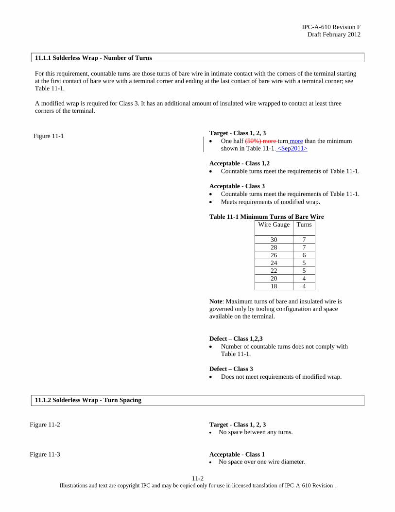
IPC-A-610 Revision F Draft February 2012
11-2 Illustrations and text are copyright IPC and may be copied only for use in licensed translation of IPC-A-610 Revision .
11.1.1 Solderless Wrap - Number of Turns For this requirement, countable turns are those turns of bare wire in intimate contact with the corners of the terminal starting at the first contact of bare wire with a terminal corner and ending at the last contact of bare wire with a terminal corner; see Table 11-1. A modified wrap is required for Class 3. It has an additional amount of insulated wire wrapped to contact at least three corners of the terminal.
Target - Class 1, 2, 3 One half (50%) more turn more than the minimum
shown in Table 11-1. <Sep2011> Acceptable - Class 1,2 Countable turns meet the requirements of Table 11-1. Acceptable - Class 3 Countable turns meet the requirements of Table 11-1. Meets requirements of modified wrap. Table 11-1 Minimum Turns of Bare Wire
Wire Gauge Turns
30 7 28 7 26 6 24 5 22 5 20 4 18 4
Note: Maximum turns of bare and insulated wire is governed only by tooling configuration and space available on the terminal. Defect – Class 1,2,3 Number of countable turns does not comply with
Table 11-1. Defect – Class 3 Does not meet requirements of modified wrap.
11.1.2 Solderless Wrap - Turn Spacing
Target - Class 1, 2, 3 No space between any turns. Acceptable - Class 1 No space over one wire diameter.
Figure 11-1
Figure 11-2
Figure 11-3
IPC-A-610 Revision F Draft February 2012
11-3 Illustrations and text are copyright IPC and may be copied only
for use in licensed translation of IPC-A-610 Revision .
Acceptable - Class 2 No space over 50% diameter of wire within
countable turns. No space over one wire diameter elsewhere. Acceptable - Class 3 No more than three turns spaced apart. No space over 50% diameter of wire within the wrap. Defect - Class 1 Any space over one wire diameter.
Defect - Class 2 Any space over half wire diameter within countable
turns. Defect - Class 3 Any space more than half wire diameter. More than three spaces any size.
11.1.3 Solderless Wrap - End Tails, Insulation Wrap
Target - Class 1,2 End tail does not protrude beyond outer surface of
wrap. Insulation reaches terminal. Target - Class 3 End tail does not protrude beyond outer surface of
wrap with insulation modified wrap (see 11.1.1). Acceptable - Class 1 Does not violate minimum electrical clearance. Exposed conductor in the insulation. Acceptable - Class 2 Insulation end meets clearance requirements to other
circuitry. End tail does not extend more than 3 mm [0.12 in]
from outer surface of wrap. Acceptable - Class 3 End tail projects no more than one wire diameter
from outer surface of wrap. Insulation must contact minimum of three corners of
post.
Figure 11-4
Figure 11-5
Figure 11-6 1. Insulation clearance 2. Wire diameter (viewed from bottom)
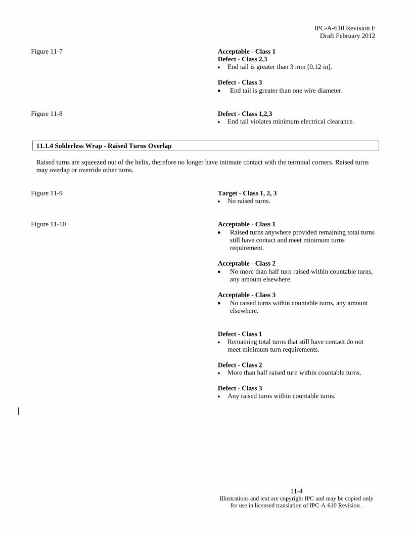
IPC-A-610 Revision F Draft February 2012
11-4 Illustrations and text are copyright IPC and may be copied only
for use in licensed translation of IPC-A-610 Revision .
Acceptable - Class 1 Defect - Class 2,3 End tail is greater than 3 mm [0.12 in]. Defect - Class 3 End tail is greater than one wire diameter. Defect - Class 1,2,3 End tail violates minimum electrical clearance.
11.1.4 Solderless Wrap - Raised Turns Overlap Raised turns are squeezed out of the helix, therefore no longer have intimate contact with the terminal corners. Raised turns may overlap or override other turns.
Target - Class 1, 2, 3 No raised turns. Acceptable - Class 1 Raised turns anywhere provided remaining total turns
still have contact and meet minimum turns requirement.
Acceptable - Class 2 No more than half turn raised within countable turns,
any amount elsewhere. Acceptable - Class 3 No raised turns within countable turns, any amount
elsewhere. Defect - Class 1 Remaining total turns that still have contact do not
meet minimum turn requirements. Defect - Class 2 More than half raised turn within countable turns. Defect - Class 3 Any raised turns within countable turns.
Figure 11-7
Figure 11-8
Figure 11-9
Figure 11-10

IPC-A-610 Revision F Draft February 2012
11-5 Illustrations and text are copyright IPC and may be copied only for use in licensed translation of IPC-A-610 Revision .
11.1.5 Solderless Wrap - Connection Position
Target - Class 1, 2, 3 All turns of each connection on working length of
terminal. Visible separation between each connection. Acceptable - Class 1,2 Extra turns of bare wire or any turns of insulated wire
(whether or not for modified wrap) beyond end of working length of terminal.
Acceptable - Class 1 Extra turns of bare wire or any turns of insulated wire
overlap a preceding wrap. Acceptable - Class 2 Turns of insulated wire only overlap a preceding
wrap. Acceptable - Class 3 Wraps may have an insulated wire overlap the last
turn of uninsulated wire. No turns of bare or insulated wire beyond either end
of working length. Defect - Class 1,2,3 Insufficient number of countable turns in contact with
the terminal. Wire overlaps the wire turns of a preceding
connection. Spacing requirements are violated. <Sep2011>
11.1.6 Solderless Wrap - Wire Dress
Acceptable - Class 1,2,3 The dress of wire needs to be oriented so that force
exerted axially on the wire will not tend to unwrap the connection, or to relieve the bite of wire on the corners of the terminal post. This requirement is satisfied when the wire is routed so as to cross the 45 line as shown.
Defect - Class 1,2,3 Axially exerted external forces on the wrap will
cause the wrap to unwind or loosen the wire bite at the post corners.
Figure 11-12
Figure 11-13 1. Wrap extends above working length 2. Insulation turn overlaps previous wrap
Figure 11-14 Figure 11-15
Figure 11-16 IPC ACTION TO MODIFY BOTTOM VIEW TO ADD INSULATION SPACING LIKE TOP VIEW 1. Direction of turns 2. Proper radius
Figure 11-17 1. Direction of turns

IPC-A-610 Revision F Draft February 2012
11-6 Illustrations and text are copyright IPC and may be copied only for use in licensed translation of IPC-A-610 Revision .
11.1.7 Solderless Wrap - Wire Slack
Acceptable - Class 1,2,3 Wiring needs to have sufficient slack so that it will not
pull around corners of the other terminal posts or bridge and load other wires.
Defect – Class 1,2,3 Insufficient wire slack causing:
Abrasion between wire insulation and wrap post. Tension on wires between wrap post causing
distortion of posts. Pressure on wires that are crossed by a taut wire.
11.1.8 Solderless Wrap – Wire Plating Plating Wire used for solderless wrap is normally plated to improve connection reliability and minimize subsequent corrosion.
Target - Class 1, 2, 3 After wrapping, uninsulated wire has no exposed
copper. Acceptable - Class 1 Any amount of exposed copper. Acceptable - Class 2 Up to 50% of countable turns show exposed copper. Defect - Class 2 More than 50% of countable turns show exposed
copper. Defect - Class 3 Any exposed copper (last half turn and wire end
excluded).
11.1.9 Solderless Wrap - Damaged Insulation
Acceptable - Class 1,2,3 After initial contact with post:
Insulation damage. Splits. Cut or frayed insulation.
Figure 11-18
Figure 11-19 1. Wire crossing
Figure 11-20
Figure 11-21 1. Initial contact corner 2. Insulation split 3. Insulation cut or frayed Figure 11-22
IPC-A-610 Revision F Draft February 2012
11-7 Illustrations and text are copyright IPC and may be copied only
for use in licensed translation of IPC-A-610 Revision .
Defect - Class 1,2,3 Minimum electrical clearance violated. Defect - Class 2,3 Splits, cuts or fraying of insulation prior to initial
contact of wire to corner of post. Spacing requirements are violated. <Sep2011>
11.1.10 Solderless Wrap - Damaged Conductors &Terminals
Target – Class 1,2,3 Wire finish is not burnished or polished, nicked,
scraped, gouged or otherwise damaged. Wire wrap terminals are not burnished, scraped or
otherwise damaged. Acceptable - Class 1,2,3 Finish on the wire is burnished or polished (slight
tool marks) (A). The top or last turn damaged from the wrap tool such
as nicks, scrapes, gouges, etc., not exceeding 25% of wire diameter (B).
Damage to terminal caused by tool such as burnishing, scraping, etc. (C)
Acceptable - Class 1,2 Defect - Class 3 Base metal is exposed on terminal.
11.2 Component Mounting – Connector Wire Dress Strain/Stress Relief <Sep2011> Wires connecting to multi-contact connectors have slack adjusted to preclude stress of individual wires.
Acceptable - Class 1,2,3 All wires are dressed with even bends to prevent
stress at contact connections. Shortest wires are in direct line with center axis of
cable. Defect - Class 1 Wires are separated from the connector. Defect - Class 2,3 Slack is inadequate to prevent stress of individual
wires.
Figure 11-23 1. Initial contact corner 2. Split insulation, etc., prior to initial contact of post. Conductor is exposed.
Figure 11-24
Figure 11-25 1. Lead dress is more critical on these wires
Figure 11-26 1. Leads are stressed
IPC-A-610 Revision F Draft February 2012
12-1 Illustrations and text are copyright IPC and may be copied only for use in licensed translation of IPC-A-610 Revision F.
12 High Voltage This section provides the unique criteria for soldered connections that are subject to high voltages, see 1.5.4. These criteria are applicable to wires or leads attached to terminals, bare terminals, and through-hole connections. The requirements are to assure that there are no sharp edges or sharp points that could initiate arcing.
Target - Class 1, 2, 3 Balled solder connection has a completely rounded,
continuous and smooth profile. No evidence of sharp edges, solder points, icicles,
inclusions (foreign material) or wire strands. Insulation clearance as close to the solder connection
as possible without interfering with formation of the required solder ball.
All edges of the terminal are completely covered with a continuous smooth layer of solder forming a solder ball.
Balled solder connection does not exceed specified height requirements.
Insulation clearance (C) is minimal so that insulation is close to the solder connection without interfering with formation of the required solder ball.
Acceptable - Class 1, 2, 3 Solder connection has an egg-shaped, spherical or
oval profile that follows the contour of terminal and wire wrap, Figure 12-1.
All sharp edges of the component lead and terminals are completely covered with a continuous smooth rounded layer of solder forming a solder ball, Figure 12-2 (A).
Solder connections may have evidence of some layering or reflow lines, see 5.2.8.
No evidence of sharp edges, solder points, icicles, inclusions (foreign material) or wire strands.
Wire/lead outline is discernible with a smooth flow of solder on wire/lead and terminal. Individual strands may be discernible, Figure 12-2 (B).
Straight-through leads facilitate ball soldering, Figure 12-2 (C).
All sharp edges of the terminal's radial split are completely covered with a continuous smooth layer of solder forming a balled solder connection.
There is no evidence of burrs or frayed edges on the hardware.
Insulation clearance (C) is less than one overall diameter (D) away from the solder connection, Figure 12-2 (D).
No evidence of insulation damage (ragged, charred, melted edges or indentations).
Balled solder connection does not exceed specified height requirements.
Figure 12-1
Figure 12-2
Figure 12-3

IPC-A-610 Revision F Draft February 2012
12-2 Illustrations and text are copyright IPC and may be copied only
for use in licensed translation of IPC-A-610 Revision F.
Defect - Class 1, 2, 3 Discernible sharp edges, solder points, icicles, or
inclusions (foreign material), Figure 12-4 (A). Evidence of edges not smooth and round with nicks
or crevices. Solder follows contour of terminal and wire wrap but
there is evidence of the sharp edge of the terminal protruding, Figure 12-4 (B).
Evidence of wire strands not completely covered or discernible in the solder connection.
Terminal lug is void of solder, Figure 12-4 (C). Hardware has burrs or frayed edges, Figure 12-4 (D). Insulation clearance (C) is one overall diameter (D)
or more, Figure 12-4 (E). Evidence of insulation damage (ragged, charred,
melted edges or indentations)., Figure 12-4 (F) Balled solder connection does not comply with height
or profile (shape) requirements.
Figure 12-4 IPC ACTION TO REKEY BOTTOM RIGHT TO F AND MAKE INSULATION DAMAGE MORE OBVIOUS