ipc-7351c revision goals.ppt · ipc-7351c revision goals 2) land pattern naming convention concept...
TRANSCRIPT

IPC-7351C Revision Goals
October 2012
John Perry, IPCTechnical Project Manager
1

IPC-7351C Revision Goals1) Zero Orientation (Pin 1 Upper Left or Lower Left)
IPC-7351B provides one orientation option (2 in the LP Calculator)IPC-2581 consortia considering one rotationEIA-471 moved to match IEC rotation
Subcommittee Feedback as of 08/28/12:
* Minor deviation exists within a few of these** Do not specifically call out IEC 61188-7 but utilize lower left or left which matches that standard.*** Compliant with the component data provided by the part manufacturer
2
IPC-7351B IEC 61188-7 EIA-481-D OTHER8* 3** 1 1***

IPC-7351C Revision Goals1) Zero Orientation (cont’d). Our reality is that the global industry uses mixed approaches to zero orientation:
Following EIA-481 is no answer as suppliers do what fits their needsFollowing the JEDEC outline is deviated from by manyDesign groups make their own decisionsIt doesn’t matter how the packages are originally described provided Rotation and Mirror are correct
Proposed Solution: Simply have IPC-7351C and IEC provide BOTH options (A &B) and let users decide which one to adopt.
This was approved by the 1-13 subcommittee at the 09/25/12 web conference
3

IPC-7351C Revision Goals2) Land Pattern Naming Convention
Concept of Land Pattern Naming Convention vs. Package Naming Convention
Component HeightComponent Manufacturer
Establish a hierarchy of required vs. optional items for the naming convention?
Identify optional data such as manufacturer part number and component heightIdentify a character that represents where the optional data begins (dashes/multiple dashes
Subcommittee Feedback to Optional Modifiers for Naming Convention provided in next few slides:
4

IPC-7351C Revision Goals2) Land Pattern Naming Convention (cont’d)
Proposed Character Separator for Optional Codes:A) Utilize the equal “=“ symbol. Repeat as necessary for optional codes.
Or B) Utilize a single letter between each optional code (e.g., T for Thermal Tab, L for Lead Length, B for BGA Ball Size, P for BGA Pin spacing)
The subcommittee agreed to item B) during the 10/09/12 web conference.
Exceptions: Height, being associated with body length and body width, would precede any equal symbol even though it is itself an optional character
*The subcommittee also agreed to add a paragraph to the “C” revision clarifying that the land pattern naming convention has more to do with the package than the actual land pattern
5
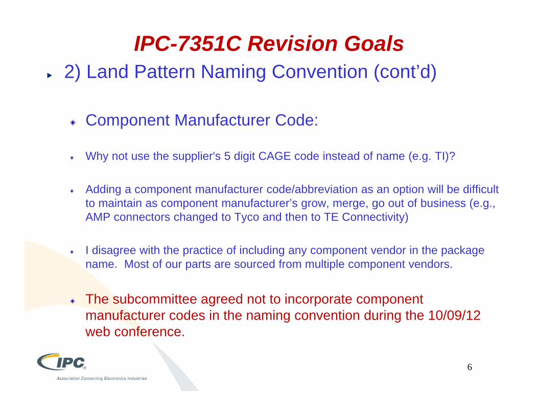
IPC-7351C Revision Goals2) Land Pattern Naming Convention (cont’d)
Component Manufacturer Code:
Why not use the supplier's 5 digit CAGE code instead of name (e.g. TI)?
Adding a component manufacturer code/abbreviation as an option will be difficult to maintain as component manufacturer’s grow, merge, go out of business (e.g., AMP connectors changed to Tyco and then to TE Connectivity)
I disagree with the practice of including any component vendor in the package name. Most of our parts are sourced from multiple component vendors.
The subcommittee agreed not to incorporate component manufacturer codes in the naming convention during the 10/09/12 web conference.
6

IPC-7351C Revision Goals3) Component Dimension Naming Convention
IPC-7351 naming convention differs from naming convention on JEDEC data sheets:
7

IPC-7351C Revision Goals3) Component Dimension Naming Convention (cont’d)
All of the inputs to the PCB Libraries Land Pattern Calculator tool indicate that component vendors are supplying their parts with JEDEC packaging naming conventions.The adoption of this naming convention for the package does not affect land pattern dimensions such as Z, G and X.The adoption of this naming convention for the package does not affect the IPC-7351 Land Pattern Naming Convention (which uses dimensions for body length and width and not alpha characters)
The subcommittee agreed to adopt the JEDEC naming convention for the components during the 10/23/2012 web conference
8

IPC-7351C Revision Goals4) Land Pattern Geometry Variations
Dieter Bergman reported that the IEC WG12 recommended the elimination of Density Level A (Maximum Land Protrusion) from the IEC-61188-5 document. Does IPC-7351C wish to follow suit?
The IEC WG12 feels that Level A does not get utilized very often anymore, and that the land patterns are much larger than need be for a robust solder joint, even for mil-aero applications. It was acknowledged that there was little to no space representation at that IEC meeting.
Our subcommittee does not agree with the complete elimination of this density level, as life expectancy (longevity) and mil-aero and space applications have dictated the usage of this density level.
Some space application product require 20,000 thermal cycle survivability
9

IPC-7351C Revision Goals4) Land Pattern Geometry Variations (cont’d)
The subcommittee proposed a compromise during the 10/23/2012 web conference that does not eliminate Density Level A altogether:
Remove Density Level A from small chip component packages, such as making the Level A column in IPC-7351C Table 3-6 blank with appropriate verbiage as to why. We need to investigate if this should be done with other component tables (LGA, CGA, etc.)
Add verbiage describing where Level A is to be used (harsh or severe environments, high thermal cycles, tin-lead, etc.)
Add verbiage describing Density Level C as the default geometry and the one used most often for lead-free applications.
McConnell and Green will search for company data that supports retaining Density Level A for space applications
10

IPC-7351C Revision Goals5) New/Modified Packages
Bottom Termination Components (BTC)IEC Proposal:
For bottom only type metallization, add 5% of the pitch to the land size (i.e., pitch of 500 µm would add 25 µm all around the land
Solder mask clearance might be 10% of the pitchUsing the pitch between lands works consistently and is intended to prevent solder bridging
Subcommittee approved IEC proposal during 11/6/12 web conference (combination of perimeter/periphery land swell plus a toe fillet)
11

IPC-7351C Revision Goals5) New/Modified Packages (cont’d)
Multiple Thermal PadsThe proliferation of segmentation of thermal tabs into multiple patterns of different sizes and shapes has increasedPCB Libraries is developing a module for their calculator tool which will have a package editor for addressing variations in thermal tabs.
Following the development of this module, the 1-13 subcommittee will determine how to draft verbiage in IPC-7351C describing how to address these unique thermal tabs.Unique Packages (Potentiometers, switches, LEDs, etc.)
These packages are virtually impossible to standardizeWe should, however, provide some guidance on how they might be named
McConnell and Hausherr will provide IPC with a listing of non-standard parts that we could draft unique packaging guidelines for
12

IPC-7351C Revision Goals6) Silkscreen OutlinesConsiderations include:
Never be located under the component because they are covered up during assembly and do not provide any function Should be mapped to the maximum component body outline and visible after assembly (based on industry feedback – had previously used nominal component body outline)Used for assembly placement registration accuracyPad to silkscreen rule overrides maximum component bodyPolarity Marking should indicate Pin 1 location and should be visible after assembly attachmentThe line width and pad to line gap are normally the sameShould always be located inside the Placement Courtyard3-Tier silkscreen lines widths
13

IPC-7351C Revision Goals6) Silkscreen Outlines (cont’d)
The preliminary IEC recommendation for 3-Tier line widths and Silkscreen to Pad Gap are illustrated in the pictures below representing a SOT23-6 component package:
Subcommittee approved the 3-tier line width concept during the 11/06/12 web conference. Also requested imagery where Pin 1 is in the middle.
14
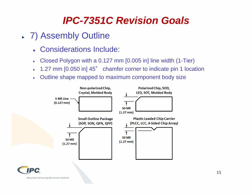
IPC-7351C Revision Goals7) Assembly Outline
Considerations Include:Closed Polygon with a 0.127 mm [0.005 in] line width (1-Tier)1.27 mm [0.050 in] 45° chamfer corner to indicate pin 1 locationOutline shape mapped to maximum component body size
15

IPC-7351C Revision Goals7) Assembly Outline (cont’d)
Considered optional for those who want to add assembly outlines to their libraryProposal designed to be as simple as possibleIs there buy-in among assembly shops for this concept? IPC should poll some assembly shops and see if this will be adopted or notPerry will submit to assembly shops participating in 7351, 001 and 610 on whether they would utilize this concept.
16

IPC-7351C Revision Goals8) Polarized Parts
Should we incorporate an option for polarity markings?
Yes! - This is actually already being addressed within the silkscreen outline, as noted in the following illustrations:
17
Component Various Silkscreen Outlines with Polarity on Pin 1
IPC-7351C Revision Goals9) Local Fiducials
Other organizations such as JEITA requesting 3 tier fiducial size
10) Courtyard ExcessProposal to change the LEAST courtyard dimension from 0.004 in to 0.005 in.
18
IPC-7351C Revision Goals11) Land Pattern Trimming
12) Land ShapesDo we want rounded rectangle land shapes as default with options for square?Maximum corner radius, radius round-off guidance
19