ionized physical vapor deposition (ipvd): technology and
TRANSCRIPT

IPVD
Ionized physical vapor deposition (IPVD):Technology and applications
Jón Tómas Guðmundsson
Science Institute, University of Iceland, IcelandDepartment of Electrical and Computer Engineering, University of Iceland, Iceland
17th International Vacuum Congress,Stockholm, Sweden, July 3. 2007

IPVD
Introduction
The demand for new materials and layer structures haslead to development of more advanced sputtering systemsWhen the flux of ions is higher than the flux of neutrals orΓ+ > Γm the process is referred to as ionized physicalvapor deposition (IPVD)In magnetron sputtering discharges this is achieved by
increasing the power to the cathode (high power pulse)a secondary discharge between the target and thesubstrate (rf coil or microwaves)reshaping the geometry of the cathode to get more focusedplasma (hollow cathodes)
Common to all highly ionized magnetron sputteringtechniques is a very high density plasma

IPVD
Introduction
Ionized Physical Vapor Deposition(IPVD)Introduction to magnetronsputteringMagnetron sputtering with asecondary discharge
Inductively coupled dischargeElectron cylclotron resonancedischarge
High power impulse magnetronsputtering discharge (HiPIMS)Hollow cathodeSummary

IPVD
Ionized Physical Vapor Deposition (IPVD)
In conventional dc magnetron sputtering the majority ofions are the ions of the inert gasThe sputtered vapor is mainly neutral, the ionizationfraction of the sputtered material is low ( ∼ 1%)
The neutral metal ejected exhibits a cosine angular velocitydistributionOver the last decade new ionized vapor depositiontechniques have appeared that achieve 50 – 90 %ionization of the sputtered materialThe development of ionized physical vapor deposition(IPVD) devices was mainly driven by the need to depositmetal layers and diffusion barriers into trenches or vias ofhigh aspect ratios. (Hopwood, 1998)

IPVD
Ionized Physical Vapor Deposition (IPVD)
The metal ions can be accelerated to the substrate bymeans of a low voltage dc bias
The metal ions arrive at the substrate at normal incidenceand at specific energyThe energy of the ions can be tailored to obtain impingingparticles with energies comparable to typical surface andmolecular binding energies
Ionizing the sputtered vapor has several advantages:
improvement of the film qualitycontrol of the reactivitydeposition on substrates with complex shapes and highaspect ratio

IPVD
Ionized Physical Vapor Deposition (IPVD)
The system design is determined by the average distancea neutral particle travels before being ionizedThe ionization mean free path is
λiz =vs
kizne
wherevs is the velocity of the sputtered neutral metalkiz is the ionization rate coefficientne is the electron density

IPVD
Ionized Physical Vapor Deposition (IPVD)
This distance has to be short
vs has to be low - thermalize the sputtered flux - increasedischarge pressurene has to be high
vs [eV] Te [eV] ne [m−3] λiz [cm]
1.5 3 1× 10¹⁷ 3330.05 3 1× 10¹⁷ 610.05 3 1× 10¹⁸ 6.10.05 3 1× 10¹⁹ 0.61

IPVD
Ionized Physical Vapor Deposition (IPVD)
Another important parameter is the fractional ionization ofthe metal flux
Γi
Γi + Γn
The ion flux to the substrate is
Γi ≈ 0.61nm+uB ∼√
Te
The flux of thermalized neutrals is
Γn =14
nmvTh ∼√
Tg
Since Te � Tg the fractional ionization of the metal flux islarger than the fraction of ionized metal in the plasmaIt is not necessary to completely ionize the sputtered metalto create a highly ionized flux to the substrate

IPVD
Planar magnetron sputtering discharge
Magnetron sputtering discharges are widely used in thinfilm processingA magnet is placed at the back of the cathode target withthe pole pieces at the center and perimeterA magnetic field confines the energetic electrons near thecathode, where they undergo numerous ionizing collisionsbefore being lost to a grounded surface

IPVD
Planar magnetron sputtering discharge
A typical dc planar magnetron discharge operates at apressure of 1 – 10 mTorr with a magnetic field strength of0.01 – 0.05 T and at cathode potentials 300 – 700 VElectron density in the substrate vicinity is in the range1015 − 1016 m−3

IPVD
Planar magnetron sputtering discharge
Conventional magnetron sputtering processes are limitedlow target utilizationtarget thermal load limits the available currentlow fraction of the sputtered material is ionized
Several sputtering systems have beendesigned to increase the ion flux at thesubstrateThey include
pulsing the applied target voltageadditional ionization by a secondarydischarge (rf or microwave)increased magnetic confinementreshaping the cathode for morefocused plasma (hollow cathode)

IPVD
Secondary discharge in a magnetron sputtering discharge
A secondary discharge is placed between the target andthe substrate in a magnetron sputtering discharge
Inductively coupled plasma (ICP) dischargeElectron cyclotron resonance (ECR) discharge
IPVD
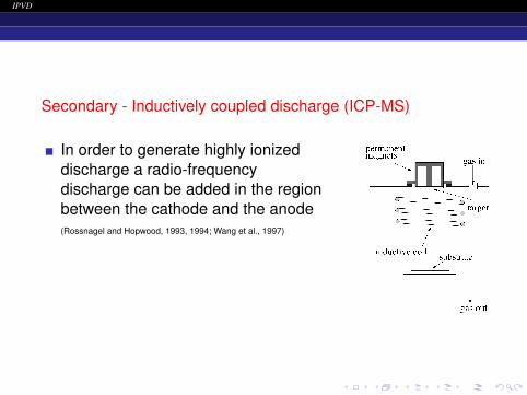
Secondary - Inductively coupled discharge (ICP-MS)
In order to generate highly ionizeddischarge a radio-frequencydischarge can be added in the regionbetween the cathode and the anode(Rossnagel and Hopwood, 1993, 1994; Wang et al., 1997)

IPVD
Secondary - Inductively coupled discharge (ICP-MS)
The ionization fraction increases andsaturates with increased rf powerThe ionization fraction saturates inthe range 20 – 80 % depending onthe discharge pressure and targetmaterialGlobal (volume averaged) modelstudy
confirms the measured ionizationfractionindicates that electron impactionization of the metal atomsdominates for electron densityabove 1017 m−3
(Hopwood, 2000)
(After Wang et al. (1999))
(After Hopwood (2000))

IPVD
Secondary - Electron cylclotron resonance discharge(ECR-MS)
A supplementary electron cyclotronresonance (ECR) discharge can beused to increase the ionization ofthe sputtered metal.ECR discharges are typicallyoperated at microwave frequencies(e.g., ∼ 2.45 GHz) with a strongmagnetic field B, giving high plasmadensities (1017 − 1018 m−3) and arecommonly operated at low workingpressures (0.1–10 mTorr).
(From Takahashi et al. (1988))
(After Xu et al. (2001))
(From Yonesu et al. (1999))

IPVD
Secondary - Electron cylclotron resonance discharge(ECR-MS)
An ECR-MS apparatus, thetwo ECR dischargechambers are located at theopposite sites of the mainprocessing chamber.A highly ionized plasma iscreated in the region betweenthe target and the substrate.(Musil et al., 1991; Takahashi et al., 1988; Xu et al.,
2001) (After Xu et al. (2001))

IPVD
Secondary discharge in a magnetron sputtering discharge
In these discharges nAr � nM and the particle balance forthe Ar plasma dictates the the electron temperature.For ICP and ECR discharges ne ∼ 1017 − 1018 m−3 so
λiz ∼ a few cm
if the sputtered vapor is thermalized
For ne � 1017 m−3, Penning ionization is the dominatingprocess for metal ionizationfor ne � 1017 m−3 the metal ions are generated by electronimpact ionization. (Hopwood, 2000)
A high level of metal ionization is to be expected since themetals (Cu, Ti, Al, Ta) have ionization potentials in therange 6 – 8 V, significantly lower than for the used inertsputtering gas atoms used.

IPVD
High power impulse magnetron sputtering discharge (HiPIMS)
In a conventional dc magnetron dischargethe power density is limited by thethermal load on the targetMost of the ion bombarding energy istransformed into heat at the targetIn unipolar pulsing the power supply is atlow (or zero) power and then a highpower pulse is supplied for a short periodThe high power pulsed magnetronsputtering discharge uses the samesputtering apparatus except the powersupply

IPVD
HiPIMS - Power supply
The high power pulsed discharge operates with aCathode voltage in the range of 500-2000 VCurrent densities of 3-4 A/cm2
Power densities in the range of 1-3 kW/cm2
Frequency in the range of 50 – 1000 HzDuty cycle in the range of 0.5 – 5 %

IPVD
HiPIMS - Power supply
0.5 mTorr (solid line), 2 mTorr (dashed line) and 20 mTorr (dot dashed line)
(After Gudmundsson et al. (2002))
The exact pulse shape is determined by the loadthe discharge formedit depends on the gas type and gas pressure

IPVD
HiPIMS - Electron density
(After Bohlmark et al. (2005))
Temporal and spatial variation of the electron densityArgon discharge at 20 mTorr with a titanium targetThe electron density in the substrate vicinity is of the orderof 1018 − 1019 m−3

IPVD
HiPIMS - Ionization fraction
There have been conflicting reports onthe ionized flux fraction
70 % for Cu (Kouznetsov et al., 1999)40 % for Ti0.5Al0.5 (Macák et al., 2000)9.5 % for Al (DeKoven et al., 2003)4.5 % for C (DeKoven et al., 2003)
The degree of ionization90 % for Ti (Bohlmark et al., 2005) (From Bohlmark et al. (2005))

IPVD
HiPIMS - Ionization fraction
To explore the ionization mechanism and the temporalbehavior of the plasma parameters a time dependentglobal (volume averaged) model was developed
The discharge is assumed to consist of
electrons, eargon atoms in the ground state, Armetastable argon atoms, Ar∗
argon ions, Ar+
metal atoms, Mmetal ions, M+

IPVD
HiPIMS - Ionization fraction
The calculated electron and ion densityversus time for Al targetThe first 100 µs electron impactionization is the most effective processin creating metal ionsThe ionized flux fraction is ∼ 99 %(Gudmundsson, 2007)
From
Ehiasarian et al. (2002)
The measuredemission froma dischargewith a Cr target

IPVD
HiPIMS - Ion energy
The time averaged ionenergy distribution for Ar+
and Ti+ ionsThe gas pressure was 3mTorr, pulse energy 3 Jand 10 J and the targetmade of TiThe ion energy distributionis broad to over 100 eVAbout 50 % of the Ti+
ions have energy > 20 eV (From Bohlmark et al. (2005))

IPVD
HiPIMS - Deposition rate
Several groups report on a significantlylower deposition rate for HIPIMS ascompared to dcMS
a factor of 2 lower deposition rate for Cuand Ti thin films (Bugaev et al., 1996)a factor of 4 – 7 lower deposition rate forreactive sputtering of TiO2 from a Titarget (Davis et al., 2004)a factor of 3 - 4 lower deposition rate forreactive sputtering of AlOx from an Altarget (Sproul et al., 2004)the reduction in deposition ratedecreases with decreased magneticconfinement (weaker magnetic field)(Bugaev et al., 1996)
IPVD
HiPIMS - Deposition rate
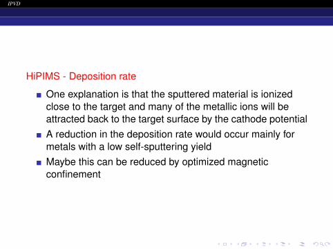
One explanation is that the sputtered material is ionizedclose to the target and many of the metallic ions will beattracted back to the target surface by the cathode potentialA reduction in the deposition rate would occur mainly formetals with a low self-sputtering yieldMaybe this can be reduced by optimized magneticconfinement

IPVD
HiPIMS - Applications
HiPIMS has already beendemonstrated on an industrial scale(Ehiasarian et al., 2006)
Due to the absence of a secondarydischarge in the reactor an industrialreactor can be upgraded to becomeIPVD device by changing the powersupply
IPVD
Other IPVD magnetron sputtering techniques
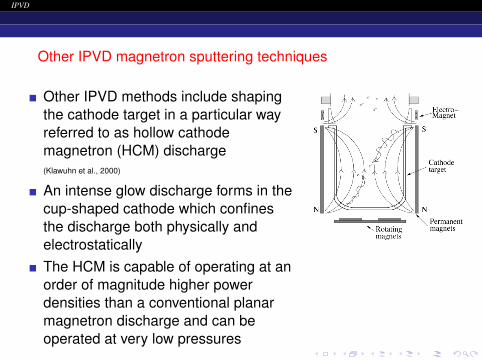
Other IPVD methods include shapingthe cathode target in a particular wayreferred to as hollow cathodemagnetron (HCM) discharge(Klawuhn et al., 2000)
An intense glow discharge forms in thecup-shaped cathode which confinesthe discharge both physically andelectrostaticallyThe HCM is capable of operating at anorder of magnitude higher powerdensities than a conventional planarmagnetron discharge and can beoperated at very low pressures

IPVD
Application - Trench filling
Ta thin films grown on Si substrates placed along a wall ofa 2 cm deep and 1 cm wide trench
conventional dc magnetron sputtering (dcMS)high power impulse magnetron sputtering (HiPIMS)
Average power is the same 440 WThey were compared by scanning electron microscope(SEM), transmission electron microscope (TEM), andAtomic Force Microscope (AFM)

IPVD
Application - Trench filling
(From Alami et al. (2005))
dcMS grown films exhibit rough surface, pores betweengrains and inclined columnar structure, leaning toward theapertureTa films grown by HiPIMS have smooth surface, and densecrystalline structure with grains perpendicular to thesubstrate

IPVD
Other applications
The advantage of IPVD for film growth has beendemonstrated by several groups
ultra-thin carbon films grown by HiPIMS have significantlyhigher densities (2.7 g/cm3), than films grown by aconventional dcMS discharge (< 2.0 g/cm3) Furthermore,the surface roughness is lower (DeKoven et al., 2003)
TiO2 thin films grown by reactive sputtering by HiPIMS havehigher index of refraction than grown by dcMS discharge -maybe due to higher density (Davis et al., 2004)
TiN thin film show increased microhardness and Yong’smodulus with increaed rf power in ICP-MS (Lim et al., 2000)
This illustrates how the bombarding ions transfermomentum to the surface allowing the microstructure to bemodified

IPVD
Summary
The technology of ionized physical vapor deposition (IPVD)has been reviewed
Addition of a secondary discharge to a magnetronsputtering discharge
Ionization fraction is controlled by power to the secondarydischarge and discharge pressure
The high power impulse magnetron sputtering discharge(HIPIMS)
Essentially the same sputtering apparatus except for thepower supplyRoughly 2 orders of magnitude higher plasma density isachieved in the substrate vicinity than for a conventional dcmagnetron sputtering dischargeIonization fraction is high, mainly due to the high electrondensity

IPVD
Summary
We demonstrated the use of a high power pulsedmagnetron sputtering discharge
for trench fillingto grow denser and harder films
IPVD
Acknowlegdements
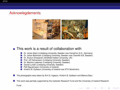
This work is a result of collaboration withDr. Jones Alami (Linköping University, Sweden now CemeCon A.G., Germany)Dr. Johan Bohlmark (Linköping University, Sweden now Chemfilt A.B. Sweden)Dr. Arutiun Ehiasarian (Sheffield Hallam University, UK)Prof. Ulf Helmersson (Linköping University, Sweden)Dr. Martina Latteman (Linköping University, Sweden)Daniel Lundin (Linköping University, Sweden)Páll Sigurjónsson (University of Iceland)Kristinn B. Gylfason (University of Iceland now KTH Stockholm)
The photographs were taken by Árni S. Ingason, Kristinn B. Gylfason and Markus Baur.
This work was partially supported by the Icelandic Research Fund and the University of Iceland Research
Fund.

IPVD
ReferencesAlami, J., P. O. A. Petersson, D. Music, J. T. Gudmundsson, J. Bohlmark, and U. Helmersson (2005). Ion-assisted
physical vapor deposition for enhanced film deposition on non-flat surfaces. Journal of Vacuum Science andTechnology A 23, 278–280.
Bohlmark, J., J. Alami, C. Christou, A. P. Ehiasarian, and U. Helmersson (2005). Ionization of sputtered metals inhigh power pulsed magnetron sputtering. Journal of Vacuum Science and Technology A 23(1), 18–22.
Bohlmark, J., J. T. Gudmundsson, J. Alami, M. Latteman, and U. Helmersson (2005). Spatial electron densitydistribution in a high-power pulsed magnetron discharge. IEEE Transactions on Plasma Science 33(2),346–347.
Bohlmark, J., M. Lattemann, J. Gudmundsson, A. Ehiasarian, Y. A. Gonzalvo, N. Brenning, and U. Helmersson(2005). The ion energy distributions and ion flux composition from a high power impulse magnetron sputteringdischarge. Thin Solid Films 515(5), 1522–1526.
Bugaev, S. P., N. N. Koval, N. S. Sochugov, and A. N. Zakharov (1996, July 21-26). Investigation of a high-currentpulsed magnetron discharge initiated in the low-pressure diffuse arc plasma. In XVIIth International Symposiumon Discharges and Electrical Insulation in Vacuum, 1996, Berkeley, CA USA, pp. 1074–1076. IEEE.
Davis, J. A., W. D. Sproul, D. J. Christie, and M. Geisler (2004). High power pulse reactive sputtering of TiO2. In47th Annual Technical Conferenece Proceedings, Dallas, TX, USA, pp. 215–218. Society of Vacuum Coaters.
DeKoven, B. M., P. R. Ward, R. E. Weiss, D. J. Christie, R. A. Scholl, W. D. Sproul, F. Tomasel, and A. Anders(2003). Carbon thin film deposition using high power pulsed magnetron sputtering. In 46th Annual TechnicalConferenece Proceedings, San Francisco, CA, USA, pp. 158–165. Society of Vacuum Coaters.
Ehiasarian, A. P., R. New, W.-D. Münz, L. Hultman, U. Helmersson, and V. Kouznetzov (2002). Influence of highpower densities on the composition of pulsed magnetron plasmas. Vacuum 65, 147–154.
Ehiasarian, A. P., C. Reinhard, P. E. Hovsepian, and J. M. Colton (2006). Industrial-scale production ofcorrosion-resistant CrN/NbN coatings deposited by combined high power impulse magnetron sputtering etchingunbalanced magnetron sputtering deposition (HIPIMS/UBM) process. In 49th Annual Technical ConfereneceProceedings, Washington DC, USA, pp. 349–353. Society of Vacuum Coaters.

IPVD
ReferencesGudmundsson, J. T. (2007). Ionization mechanism in the high power impulse magnetron sputtering (HiPIMS)
discharge. Journal of Physics: Conference Series (submitted)
Gudmundsson, J. T., J. Alami, and U. Helmersson (2002). Spatial and temporal behavior of the plasma parametersin a pulsed magnetron discharge. Surface and Coatings Technology 161(2-3), 249–256.
Gylfason, K. B., J. Alami, U. Helmersson, and J. T. Gudmundsson (2005). Ion-acoustic solitary waves in a pulsedmagnetron sputtering discharge. Journal of Physics D: Applied Physics 38(18), 3417–3421.
Helmersson, U., M. Lattemann, J. Alami, J. Bohlmark, A. P. Ehiasarian, and J. T. Gudmundsson (2005). High powerimpulse magnetron sputtering discharges and thin film growth: A brief review. In 48th Annual TechnicalConferenece Proceedings, Denver, CO, USA, pp. 458 – 464. Society of Vacuum Coaters.
Helmersson, U., M. Lattemann, J. Bohlmark, A. P. Ehiasarian, and J. T. Gudmundsson (2006). Ionized physicalvapor deposition (IPVD): A review of technology and applications. Thin Solid Films 513(1-2), 1–24.
Hopwood, J. (1998). Ionized physical vapor deposition of integrated circuit interconnects. Physics of Plasmas 5(5),1624–1631.
Hopwood, J. A. (2000). Plasma physics. In J. A. Hopwood (Ed.), Thin Films: Ionized Physical Vapor Deposition, pp.181–207. San Diego: Academic Press.
Klawuhn, E., G. C. D’Couto, K. A. Ashtiani, P. Rymer, M. A. Biberger, and K. B. Levy (2000). Ionized physical-vapordeposition using a hollow-cathode magnetron source for advanced metallization. Journal of Vacuum Scienceand Technology A 18, 1546 – 1549.
Kouznetsov, V., K. Macák, J. M. Schneider, U. Helmersson, and I. Petrov (1999). A novel pulsed magnetron sputtertechnique utilizing very high target power densities. Surface and Coatings Technology 122(2-3), 290–293.
Lim, J.-W., H.-S. Park, T.-H. Park, J.-J. Lee, and J. Joo (2000). Mechanical properties of titanium nitride coatingsdeposited by inductively coupled plasma assisted direct current magnetron sputtering. Journal of VacuumScience and Technology A 18(2), 524–528.
Macák, K., V. Kouznetzov, J. M. Schneider, U. Helmersson, and I. Petrov (2000). Ionized sputter deposition using anextremely high plasma density pulsed magnetron discharge. Journal of Vacuum Science and TechnologyA 18(4), 1533–1537.

IPVD
ReferencesMusil, J., S. Kadlec, and W.-D. Münz (1991). Unbalanced magnetrons and new sputtering systems with enhanced
plasma ionization. Journal of Vacuum Science and Technology A 9(3), 1171 – 1177.
Rossnagel, S. M. and J. Hopwood (1993). Magnetron sputter deposition with high levels of metal ionization. AppliedPhysics Letters 63(24), 3285–3287.
Rossnagel, S. M. and J. Hopwood (1994). Metal ion deposition from ionized magnetron sputtering discharge.Journal of Vacuum Science and Technology B 12, 449–453.
Sproul, W., D. J. Christie, and D. C. Carter (2004). The reactive sputter deposition of aluminum oxide coatings usinghigh power pulsed magnetron sputtering (hppms). In 47th Annual Technical Conferenece Proceedings, Dallas,TX, USA, pp. 96–100. Society of Vacuum Coaters.
Takahashi, C., M. Kiuchi, T. Ono, and S. Matsuo (1988). An electron cyclotron resonance plasma depositiontechnique employing magnetron mode sputtering. Journal of Vacuum Science and Technology A 6(4),2348–2352.
Wang, W., J. Foster, T. Snodgrass, A. E. Wendt, and J. H. Booske (1999). An rf sustained argon and copper plasmafor ionized physical vapor deposition of copper. Journal of Applied Physics 85, 7556–7561.
Wang, W., J. Foster, A. E. Wendt, J. H. Booske, T. Onuoha, P. W. Sandstrom, H. Liu, S. S. Gerhard, andN. Hershkowitz (1997). Magnetic-field-enhanced rf argon plasma for ionized sputtering of copper. AppliedPhysics Letters 71, 1622–1624.
Xu, J., X. Deng, J. Zhang, W. Lu, and T. Ma (2001). Characterization of CNx films prepared by twinned ECR plasmasource enhanced DC magnetron sputtering. Thin Solid Films 390(1-2), 107 – 112.
Yonesu, A., T. Kato, H. Takemoto, N. Nishimura, and Y. Yamashiro (1999). Cylindrical DC magnetron sputteringassisted by microwave plasma. Japanese Journal of Applied Physics 38, 4326 – 4328.