investigation of wire electrical discharge machining of thin cross-sections and compliant mechanisms
TRANSCRIPT
Investigation of wire electrical discharge machining of thin
cross-sections and compliant mechanisms
Scott F. Millera, Chen-C. Kaoa, Albert J. Shiha,*, Jun Qub
aMechanical Engineering, University of Michigan, Ann Arbor, MI 48109, USAbOak Ridge National Laboratory, Metals and Ceramics Division, Oak Ridge, TN 37831, USA
Received 30 September 2004; accepted 3 March 2005
Available online 12 April 2005
Abstract
The wire electrical discharge machining (EDM) of cross-section with minimum thickness and compliant mechanisms is studied. Effects of
EDM process parameters, particularly the spark cycle time and spark on-time on thin cross-section cutting of Nd–Fe–B magnetic material,
carbon bipolar plate, and titanium are investigated. An envelope of feasible wire EDM process parameters is generated for the commercially
pure titanium. The application of such envelope to select suitable EDM process parameters for micro feature generation is demonstrated.
Scanning electron microscopy (SEM) analysis of EDM surface, subsurface, and debris are presented. SEM observations lead to a hypothesis
based on the thermal and electrostatic stress induced fracture to explain the limiting factor for wire EDM cutting of thin-sections.
Applications of the thin cross-section EDM cutting for manufacture of compliant mechanisms are discussed.
q 2005 Elsevier Ltd. All rights reserved.
Keywords: Wire EDM; Compliant mechanism; Material removal rate
1. Introduction
The development of micro mechanical components, the
growing needs for micro-feature generation, and appli-
cations of advanced, difficult-to-machine materials have
made the wire EDM an important manufacturing process to
meet these demands. The wire EDM process uses electrical
sparks between a thin, traveling wire electrode and the
workpiece to erode the work-material and generate
the desired shapes. The cutting force is low, which makes
the EDM an important process to manufacture precise,
intricate, and miniature features on mechanical components.
The information to select proper wire EDM process
parameters for newly developed materials or micro features
is not readily available [1]. Manufacturers of EDM
machines usually provide a database of suggested process
parameters for commonly used work- and electrode-
materials under typical operating conditions. Such database
cannot meet the growing new EDM applications, including
0890-6955/$ - see front matter q 2005 Elsevier Ltd. All rights reserved.
doi:10.1016/j.ijmachtools.2005.03.003
* Corresponding author. Tel.: C1 734 647 1766; fax: C1 734 936 0363.
E-mail address: [email protected] (A.J. Shih).
the machining of miniature features. The goal of this study
is to investigate the effect of two important wire EDM
process parameters, spark cycle and spark on-time, on the
thin-section cutting of sintered Nd–Fe–B magnet, titanium,
and carbon–carbon bipolar plate.
The EDM machine converts the electrical energy into
thermal energy in the plasma discharge channel during the
spark discharge. The thermal energy melts and vaporizes
workpiece material during the process. The molten work-
and electrode-materials solidify on the work surface and
create a recast layer [2]. The high temperature has two
effects. First, a heat affected zone under the recast layer is
created [2]. Second, the high temperature generates the
thermal stress in the workpiece. As will be seen in this
research, the thermal stress could affect the minimum
thickness of the workpiece in wire EDM.
The micro EDM has been studied extensively by
Masuzawa and his research group in the past two decades
[3–5]. In addition, Luo [6] investigated the EDM with a
small erosion area by examining effects of spark off time.
Takahata and Gianchandani [7] studied the use of electrode
arrays for batch EDM generation of micro-features.
Furutani et al. [8,9] developed the dot-matrix EDM method
using the thin wire electrode to produce various micro
International Journal of Machine Tools & Manufacture 45 (2005) 1717–1725
www.elsevier.com/locate/ijmactool
Vol
tage
Time
Ton
T
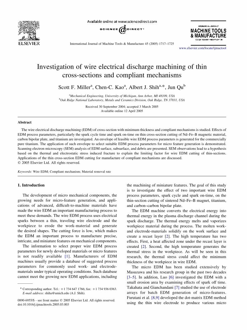
Fig. 1. Definition of the spark cycle, T, and spark on-time, Ton, in the EDM
spark cycle.
S.F. Miller et al. / International Journal of Machine Tools & Manufacture 45 (2005) 1717–17251718
shapes with the mm level accuracy. Rajurkar and Yu [10]
expanded the micro EDM technology using CAD/CAM.
Hori and Murata [11] studied the wire EDM of micro
involute spur gears. Yu et al. [12] presented a theoretical
model for micro EDM surface profile generation and
incorporating the tool wear effect. More recently, Kaminski
and Capuano [13] and Zhao et al. [14] studied the EDM
micro hole machining.
An envelope of material removal rate (MRR)
was defined and generated for a variety of advanced
materials to aid the selection of process parameters for
wire EDM [1,15]. Such envelope can be applied to setup the
wire EDM process for fast, high MRR machining. A rough
surface with a thick recast layer is usually generated in high
MRR EDM. Another application of the wire EDM
envelope, more relevant to this study, is the selection of
process parameters for slow, low MRR EDM cutting to
enable the machining of micro-features and generate
surfaces with improved integrity. In this study, the envelope
of feasible wire EDM process parameters for commercially
pure titanium, denoted as Ti, is created. The envelope is
employed to machine the Ti with thin cross-section. The Ti
material is selected because of its biocompatibility for
human implant applications.
This study explores the use of wire EDM for manufac-
turing of compliant mechanisms. Compliant mechanisms
are defined as the jointless mechanisms where the elastic
deformation is intended as a source of motion [16]. The
thin-section is used to generate the deformation and motion
of compliant mechanisms. Wire EDM is a process of choice
for the fabrication of compliant mechanisms. Wire EDM of
miniature titanium compliant mechanisms, which have the
potential for medical applications, is investigated. The MRR
process envelope of Ti is applied to select suitable EDM
process parameters.
The experimental setup and procedure of the wire EDM
machine are first discussed. Results of the Ti MRR envelope
and thin cross-section cutting of various materials are then
presented. The scanning electron microscope (SEM) is
applied to analyze debris captured in wire EDM. The effect
of thermal stress on thin-section wire EDM is investigated.
Finally, applications of micro-feature generation, including
the compliant mechanism, are discussed.
2. Experimental setup and work-materials
2.1. Wire EDM machine setup
The EDM experiments are conducted on a Brother
HS-5100 wire EDM machine using the brass wire with
0.25 mm nominal diameter. Two EDM process parameters
studied are the spark cycle, T, and spark-on time, Ton. Fig. 1
shows a typical waveform of voltage between the workpiece
and wire electrode during EDM. The spark cycle, T, is the
period of change in voltage. The spark on-time or pulse
on-time, Ton, is the duration in a spark cycle that the voltage
is built up. For the Brother HS-5100, the range of spark on-
time (Ton) is from 2 to 18 ms and spark cycle, T, is from 10 to
1000 ms. The wire tension is 15 N, and the gap voltage
between the wire and electrode was set at 35 V.
2.2. Work-materials
Three work materials investigated in this study are the
sintered Nd–Fe–B permanent magnet, grade two commer-
cially pure Ti, and carbon–carbon bipolar plate. Properties
of Nd–Fe–B magnet, which has high magnetic density
and is used for miniature, energy-efficient electrical motor,
actuator, and generator applications, and the carbon–
carbon bipolar plate, which is used for proton exchange
membrane fuel cell, have been discussed in the previous
research [1,15].
2.3. Experimental setup and procedure
The 1.5 mm thick Nd–Fe–B plate, 2.3 mm thick carbon–
carbon bipolar plate, and 1 mm thick Ti plate are used to
investigate the effect of T and Ton on the thin-section EDM
cutting. The envelope of feasible wire EDM process
parameters for Nd–Fe–B and carbon–carbon bipolar plate
have been presented in Ref. [1] and are applied for both high
and low MRR EDM cutting. The high MRR EDM cutting
requires high energy density, creates thick recast layers and
surface damages, and limits the minimum thickness in thin-
section cutting. On the contrary, the low MRR EDM is a
slow process, but it is more suitable for machining thin-
sections and micro-features.
The setup of thin-section EDM cutting experiment is
shown in Fig. 2. The EDM cuts parallel grooves in a plate
and leaves a thin section of thickness t. The same set of
process parameter is repeated and the thickness cut is
reduced each time until the minimum thickness of the thin-
section is achieved.
Tests are conducted to find minimum thickness for a
specific Ton. When the Ton is high, the electrical spark
energy is strong, thermal shock due to thermal stress is

Thin sectionEDM wire
Work-material
t
w
Fig. 2. Wire EDM experiment setup to cut thin section.
0
5
10
15
20
25
30
0 100 200 300 400 500 600 700
Spark Cycle (µs)
Fee
d R
ate
(mm
/min
)
Ton=18µsTon=14µsTon=10µsTon=6µsTon=2µsWire breakShort circuit
Fig. 3. Envelope of feasible wire EDM process parameters for Ti.
S.F. Miller et al. / International Journal of Machine Tools & Manufacture 45 (2005) 1717–1725 1719
large, and wire feed rate or MRR is high. On the other
extreme, when Ton is low, the electrical spark energy is
weak, energy delivered during cutting is small, and wire
feed rate or MRR is low. The MRR is usually high at higher
Ton. The minimum thickness in wire EDM, as observed in
this study, is more dependent on Ton than T.
The machine, material, and physical limitations such as
debris flushing determine the minimum thickness in wire
EDM thin section cutting. To determine the feasible
envelope, sets of wire EDM tests are first conducted for
specific pulse on-time, Ton, at 2, 6, 10, 14, and 18 ms. For the
wire EDM machine used in this study, 2 and 18 ms are the
lower and upper limits for Ton, respectively. Under the same
Ton, the spark cycle, T, is varied. Without knowing the
behavior of new work-materials processed by EDM,
different levels of T have to be tested. To determine the
minimum thickness of the thin section under certain spark
energy, the binary-section method was applied. First, a
relatively large thickness (t0) for cutting was tried. Then the
second thickness was set to be tZt0/2. If this succeeded,
tested thickness was tZ t0/4, otherwise tZ3t0/4 was tested.
The same step was repeated until the change in thickness
value was close to 25 mm. The length of cut is at least 3 mm,
about 12 times the diameter of the wire.
3. Wire EDM experimental results
3.1. Ti MRR envelope and thin-section cutting
The wire EDM MRR envelope of the feasible T and Ton
for 1 mm thick Ti is generated. The Ti material and its MRR
envelope are then applied for the thin-section cutting and
later, in Section 6, for machining of compliant mechanisms.
The experimental procedure to find the envelope of
feasible T under a specific Ton has been presented in [1]. For
a set Ton, the machine limits of short circuit and wire
breakage constrains the T and MRR. Limits imposed by the
EDM machine used in this study, including the 2–18 ms Ton
and the maximum slide speed, complete the boundaries of
an envelope.
The wire EDM envelope for 1 mm thick Ti is shown in
Fig. 3. The TonZ18 and 2 ms are the top and bottom
boundaries. The wire break and short circuit are the left and
right boundaries, respectively. Compared to other envelopes
presented in [1], the Ti has a broad selection of MRR at low
spark cycle T. For example, at TZ60 ms, a wide range of
feed rate, from almost the highest 27 mm/min to the lowest
0.5 mm/min, can be achieved. Two process conditions at
two extreme sides of TZ100 ms, i.e. TonZ2 and 18 ms, are
used in the following thin-section EDM cutting tests.
Results of thin-section cutting of Ti with TonZ2 and
18 ms are shown in Fig. 4(a) and (b), respectively. Fig. 4(a)
illustrates the 61 mm thickness section machined using
TonZ2 ms and 0.5 mm/min wire feed rate. The MRR is
small but thinner cross-section can be machined. When the
Ton is increased to 18 ms, the wire feed rate is increased to
26 mm/min but the minimum thickness is increased to
165 mm. This illustrates the effect of EDM process
parameter selection on micro-feature generation.
Another phenomenon observed in Fig. 4 is the bending of
thin-section to the right. All grooves were cut from left to
right. The bending is due to the thermal stress generated
during the EDM process.
3.2. Carbon–carbon bipolar plate and Nd–Fe–B magnet
thin-section cutting
For the carbon–carbon bipolar plate, two sets of process
parameter with the highest MRR (TonZ18 ms and TZ60 ms)
and lowest MRR (TonZ4 ms and TZ1000 ms) are experi-
mented. The minimum thickness of the section cut by the
wire EDM, as shown in Fig. 5(a), is 2.7 mm for the high
MRR and 1.2 mm for the low MRR EDM cutting.
Another set of thin section wire EDM tests was
conducted on the sintered Nd–Fe–B magnet. Results are
shown in Fig. 5(b). Under TonZ2, 10, and 18 ms with
respective TZ80, 120, and 150 ms, the minimum thickness
is 0.20, 0.75, and 1.15 mm, respectively, for the Nd–Fe–B
magnet. The flushing of de-ionized water was applied
during the EDM process.
The effect of water flushing on the minimum thickness
was also experimented. Table 1 compares results from EDM

Fig. 4. Results of thin-section wire EDM of Ti with TZ100 ms: (a) TonZ2 ms and (b) TonZ18 ms. Noted the grooves cut from left to right and the bending
created by thermal stress.
S.F. Miller et al. / International Journal of Machine Tools & Manufacture 45 (2005) 1717–17251720
thin-section tests with and without water flushing. It is noted
that flushing will clean the debris from the gap between wire
electrode and workpiece and can improve the MRR.
However, flushing generates a force on the workpiece.
This force can be detrimental for the thin-section or micro-
feature machining due to the bending and possibly
fracturing of the miniature workpiece during EDM. Results
in Table 1 show that a smaller minimum thickness can be
obtained without the water flushing.
4. SEM investigation
The SEM is applied to examine the surface, subsurface
cross-section, and debris of the wire EDM cut thin-section
to gain insight of possible causes that limit the EDM thin-
section cutting.
Fig. 5. Minimum thickness by wire EDM thin-section of: (a)
4.1. Nd–Fe–B thin-section
Fig. 6 shows SEM micrographs of three Nd–Fe–B
magnet thin-sections shown in Fig. 3. These three thin-
sections were machined by wire EDM with respective Ton
settings of 18, 10, and 6 ms. The roughness of the surface
was measured using a Taylor Hobson Form Taylorsurf
contact profilometer. The measured values of arithmetic
surface roughness Ra, also shown in Fig. 6, are 3.40, 1.16,
and 0.90 mm for TonZ18, 10, and 6 ms, respectively.
Rougher surface with larger crater and deeper subsurface
damage can be identified on the EDM Nd–Fe–B thin-
section. Below the thin surface recast layer, there does not
seem to be much difference on the three Nd–Fe–B samples.
This observation of the shallow subsurface damage is a step
toward the hypothesis for limited thickness of cross-section
in wire EDM cutting.
carbon–carbon bipolar plate and (b) Nd–Fe–B magnet.

Table 1
EDM thin section cutting of sintered Nd–Fe–B magnet
With water flushing Without water flushing
Ton (ms) T (ms) Minimum
thickness
(mm)
Ton (ms) T (ms) Minimum
thickness
(mm)
2 80 0.20 2 80 0.15
10 120 0.75 6 80 0.35
18 150 1.15 10 80 0.53
14 120 0.67
18 200 0.95
Fig. 6. SEM micrographs of surface and cross-section of the subsurface
S.F. Miller et al. / International Journal of Machine Tools & Manufacture 45 (2005) 1717–1725 1721
4.2. Nd–Fe–B debris
A trap made of filter paper is set up in the wire EDM
machine to capture the EDM debris during machining.
Debris in two tests, one during regular EDM cutting
and another during the failed thin-section EDM cutting,
are captured and examined using the SEM. The failed
thin-section EDM cutting means the setup for EDM
cutting a section with thickness slightly smaller than the
known minimum thickness. The intent is to observe the
EDM debris to gain insight on wire EDM of thin cross-
section.
generated on the Nd–Fe–B thin-section machined by wire EDM.
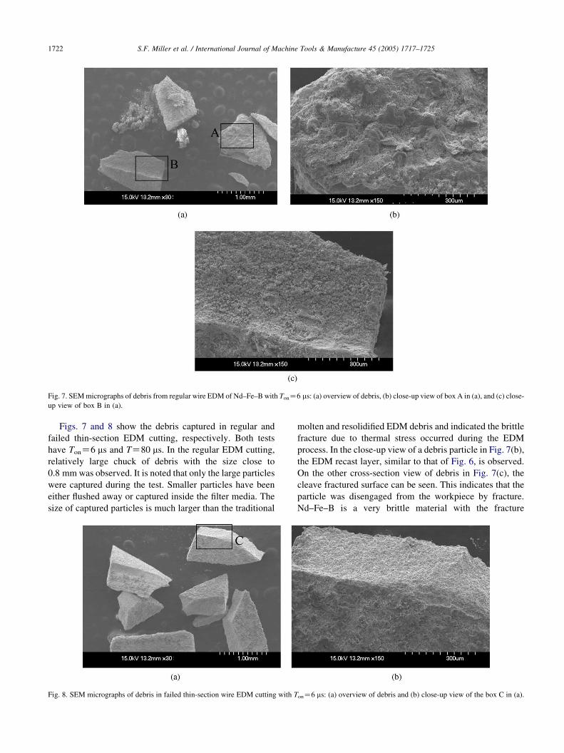
Fig. 7. SEM micrographs of debris from regular wire EDM of Nd–Fe–B with TonZ6 ms: (a) overview of debris, (b) close-up view of box A in (a), and (c) close-
up view of box B in (a).
S.F. Miller et al. / International Journal of Machine Tools & Manufacture 45 (2005) 1717–17251722
Figs. 7 and 8 show the debris captured in regular and
failed thin-section EDM cutting, respectively. Both tests
have TonZ6 ms and TZ80 ms. In the regular EDM cutting,
relatively large chuck of debris with the size close to
0.8 mm was observed. It is noted that only the large particles
were captured during the test. Smaller particles have been
either flushed away or captured inside the filter media. The
size of captured particles is much larger than the traditional
Fig. 8. SEM micrographs of debris in failed thin-section wire EDM cutting with T
molten and resolidified EDM debris and indicated the brittle
fracture due to thermal stress occurred during the EDM
process. In the close-up view of a debris particle in Fig. 7(b),
the EDM recast layer, similar to that of Fig. 6, is observed.
On the other cross-section view of debris in Fig. 7(c), the
cleave fractured surface can be seen. This indicates that the
particle was disengaged from the workpiece by fracture.
Nd–Fe–B is a very brittle material with the fracture
onZ6 ms: (a) overview of debris and (b) close-up view of the box C in (a).

S.F. Miller et al. / International Journal of Machine Tools & Manufacture 45 (2005) 1717–1725 1723
toughness KIC only in the 2.5–5.5 MPa m1/2 [17]. Its
resistance to tensile stress produced by thermal shock is
not good. The same phenomenon of thermal cracking the
Nd–Fe–B material can also be identified in Fig. 8 for the
debris particle of failed thin-section cutting. Large, about
0.9 mm size, debris with clear cleave surface is observed.
The Nd–Fe–B debris collected in regular EDM and failed
thin-section EDM with TonZ10 ms and TZ80 ms are also
examined using the SEM. The same conclusion, as
demonstrated in Figs. 7 and 8, is reached.
5. Hypothesis of fracture in EDM thin-section cutting
The observations in Figs. 6–8 indicate that the stress
fracture, particularly the tensile stress for the brittle Nd–Fe–B,
limits the thickness in thin-section wire EDM cutting. Two
possible sources of stress that causes the fracture are the
thermal stress and electrostatic stress.
EDM is a thermal process and thermal stress is generated
around the crater after the spark erosion. Yadav et al. [18] has
applied the finite element method to analyze the thermal stress
induced by a single spark in EDM of Cr die steel. The high
temperature gradient is observed in a small heat affected zone
as deep as 0.1 mm. The thermal stress was large and
dominated by tensile stresses. Such high thermal stress can
cause the fracture in thin-section cutting of the brittle Nd–Fe–
B work-material.
This study extended the finite element analysis of thermal
stress to the specific thin-section EDM cutting configuration.
The coupled temperature and stress analysis using ANSYS
finite element analysis software is conducted. The
finite element mesh used in this analysis is shown in
Fig. 9(a). The 2D 4-node plane stress finite element is
Fig. 9. Finite element prediction of the temperature and thermal stress in thin-sectio
temperature, and (c) contour of von Mises stress.
selected. For the coupled analysis, each node has three
degree-of-freedom: the temperature and displacements in X
and Y directions. The Nd–Fe–B workpiece is 2.15 mm high
and 1.16 mm wide. The width of the groove and the diameter
of the semi-circle at the end of groove is 0.3 mm. The depth of
the groove is 1.15 mm. Width of the thin-section is 0.06 mm.
The entire surrounding region is under force convection
cooling except the semi-circular front region of the groove,
which is assumed to be 1620 K, melting temperature of
sintered Nd–Fe–B, for a period of 18 ms, the duration of Ton.
After the first 18 ms of heating, the semi-circular region, like
all the other surrounding regions, is cooled by convective
heat transfer in the next 62 ms to make the 80 ms spark cycle.
Another spark duration of 18 ms and 1620 K on the semi-
circular region of the groove is applied and then followed by
the 62 ms cooling. The same 18 ms heating and 62 ms cooling
procedure repeats for the third time. The transient, coupled
thermal and stress analysis was performed. In the stress
analysis, the bottom right corner node is fixed in the X and Y
directions and the bottom left node is fixed only in the
Y direction. Material properties used for the input are:
7500 kg/m3 density, 160 GPa Young’s modulus, 0.24
Poison’s ratio, 420 J/kg K heat capacity, 9 W/m K thermal
conductivity, 3 mm/m K thermal expansion coefficient, and
2000 W/m2 K forced convection coefficient.
The temperature and stress distributions at the end of
three spark cycles (240 ms after the start of the first spark)
are illustrated in Fig. 9(b) and (c). A thin layer of high
temperature at about 980 K is concentrated in front of the
semi-circular groove region. High tensile thermal stress at
about 250 MPa, which is the same value as the flexural
strength of Nd–Fe–B, is located close to the semi-circular
groove region where the periodical melting temperature
applied. The EDM subsurface has cracks and other
n cutting: (a) finite element mesh and boundary condition and (b) contour of

Fig. 10. A 0.1 mm thick 3 mm!3 mm Ti square machined using wire EDM: (a) overview and (b) close-up view of the 0.101 mm thick section.
S.F. Miller et al. / International Journal of Machine Tools & Manufacture 45 (2005) 1717–17251724
damages, the flexural strength is expected to much lower
than the 250 MPa level. At the location close to the thin-
section, the thermal stress is very low, less than 28 MPa. It is
likely that only thermal stress alone is not adequate to
fracture the thin-section.
Another possible cause of the material removal in EDM,
as presented by Singh and Ghosh [19], is the electrostatic
force. For very short spark on-time (Ton!5 ms), the work-
material does not have enough time to get the adequate heat
for melting. The electrostatic force acting on the surface
becomes an important factor for material removal.
It is likely the combination of both thermal and
electrostatic stress dominate the cross-section thickness. A
further study is underway to model the combined stress to
fracture the thin-section in EDM cutting.
6. Application for Ti compliant mechanism
manufacturing
The knowledge gained from wire EDM thin-section
cutting is applied to manufacture compliant mechanisms.
Fig. 11. The variable-focus reflector compliant mechanism: (a) description and
Two examples, both using 1 mm thick Ti plate as the blank,
are presented. Fig. 10(a) shows a 3.5 mm!3.5 mm Ti
square with 0.1 mm section thickness cut by the wire EDM.
The close-up view of one of four corners and the 0.101 mm
cross-section thickness, measured using an optical micro-
scope, is shown in Fig. 10(b).
Another example is a Ti compliant mechanism used for
variable-focus reflector. This compliant mechanism, as
shown in Fig. 11, is about 11 mm!9 mm in size.
Fig. 11(a) explains the function of the variable-focus
reflector. With the top anchor fixed, the input port in the
bottom can be controlled by a piezoelectric actuator to
change the curvature and focal length of the top curved
region. The thickness of the in-plane cross-section ranges
from 0.10 to 0.20 mm, whereas the out-of-plane thickness
is 1 mm. The process parameters for fabrication of
miniature compliant mechanisms are obtained from the
envelope of MRR of Ti (Fig. 3). Two sets of EDM
process parameters, corresponding to the high MRR
(TonZ18 ms and TZ80 ms) and another to the low
MRR (TonZ2 ms and TZ60 ms), are investigated. The
low MRR setting was the process parameter used to
(b) wire EDM mechanism with about 0.1 mm in thickness (TonZ2 ms).

S.F. Miller et al. / International Journal of Machine Tools & Manufacture 45 (2005) 1717–1725 1725
produce the compliant mechanism shown in Fig. 11(b).
The fabrication was not successful with the high MRR for
the 0.1 mm section thickness.
7. Concluding remarks
Effects of spark cycle and pulse on-time on wire EDM
micro features were investigated. Tests were conducted on
various materials for minimum thickness wire EDM
cutting. Applications of low MRR EDM cutting for
machining of thin-section and compliant mechanisms
were studied. A hypothesis was proposed based on the
combined thermal and electrostatic force to cause the
fracture of thin-section during wire EDM. This was
supported by findings from SEM micrographs of EDM
surface, subsurface, and debris. Further in-depth research
is required to understand the root-cause for the material
fracture mechanism.
This study presented the needs of detailed thermal and
electrostatic stress modeling for micro EDM, particularly
for components with miniature feature size. Although
results presented are machine-dependent, this research
provides the guidelines and procedures for the development
of wire EDM process to manufacture miniature features on
advanced engineering materials.
Acknowledgements
The authors acknowledge Magnequench and Dr B.M.
Ma for the sintered Nd–Fe–B permanent magnets, Porvair
PLC, Dr K. Butcher for the metal foam and carbon–carbon
bipolar plate, Dr S. Kota on the design specification of
compliant mechanisms, Enhui Shi for machine operation,
and Rui Li for finite element analysis. A portion of this
research was sponsored by the Assistant Secretary for
Energy Efficiency and Renewable Energy, Office of
Transportation Technologies, as part of the High Tempera-
ture Materials Laboratory User Program, Oak Ridge
National Laboratory, managed by UT-Battelle, LLC for
the U.S. Department of Energy under contract number DE-
AC05-00OR22725.
References
[1] S.F. Miller, A.J. Shih, J. Qu, Investigation of the spark cycle on
material removal rate in wire electrical discharge machining of
advanced materials, International Journal of Machine Tools and
Manufacture 44 (2004) 391–400.
[2] J. Qu, A.J. Shih, R.O. Scattergood, Development of the cylindrical
wire electrical discharge machining process: part II: surface integrity
and roundness, Journal of Manufacturing Science and Engineering
124 (4) (2002) 708–714.
[3] T. Masuzawa, H.K. Tonshoff, Three-dimensional micromachining by
machine tools, Annals of the CIRP 46 (1997) 621–628.
[4] Z.Y. Yu, T. Masuzawa, M. Fujino, Micro-EDM for three-dimensional
cavities-development of uniform wear method, Annals of the CIRP 47
(1998) 169–172.
[5] T. Masuzawa, K. Okajima, T. Taguchi, M. Fujino, EDM-lathe for
micromachining, Annals of the CIRP 51 (1) (2002) 355–358.
[6] Y.F. Luo, An investigation into the actual EDM off-time in SEA
machining, Journal of Materials Processing Technology 74 (1998)
61–68.
[7] K. Takahata, Y.B. Gianchandani, Batch mode micro-electro-dis-
charge machining, Journal of Microelectromechanical Systems 11 (2)
(2002) 102–110.
[8] K. Furutani, T. Enami, N. Mohri, Three-dimensional shaping by dot-
matrix electrical discharge machining, Precision Engineering 21
(1997) 65–71.
[9] K. Furutani, T. Enami, N. Mohri, Dot-matrix electrical discharge
machining for shaping fine structure, Proceedings of the IEEE Micro
Electro Mechanical Systems (MEMS) 1997; 180–185.
[10] K.P. Rajurkar, Z.Y. Yu, 3D micro-EDM using CAD/CAM, Annals of
the CIRP 49 (2000) 127–130.
[11] K. Hori, Y. Murata, Wire electrical discharge machining of micro-
involute gears, Transactions of the Japan Society of Mechanical
Engineers, Part C 60 (1994) 3957–3962.
[12] Z.Y. Yu, J. Kozak, K.P. Rajurkar, Modeling and simulation of micro
EDM process, Annals of the CIRP 52 (2003) 143–146.
[13] P.C. Kaminski, M.N. Capuano, Micro hole machining by conven-
tional penetration electrical discharge machine, International Journal
of Machine Tools and Manufacture 43 (2003) 1143–1149.
[14] W. Zhao, Z. Wang, S. Di, G. Chi, H. Wei, Ultrasonic and electrical
discharge machining to deep and small hole on titanium alloy, Journal
of Materials Processing Technology 120 (2002) 101–106.
[15] S.F. Miller, A.J. Shih, Investigation the effect of spark cycle on the
material removal rate in wire electrical discharge machining. 2003
ASME IMECE, Washington, DC, November 16–21, 2003.
[16] L.L. Howell, Compliant Mechanisms, Wiley, London, 2002.
[17] J.A. Horton, J.W. Herchenroder, Fracture toughness of commercial
magnets, IEEE Transactions on Magnets 32 (1996) 4374–4376.
[18] V. Yadav, V.K. Jain, P.M. Dixit, Thermal stresses due to electrical
discharge machining, International Journal of Machine Tools and
Manufacture 42 (2002) 877–888.
[19] A. Singh, A. Ghosh, A thermo-electric model of material removal
during electric discharge machining, International Journal of Machine
Tools and Manufacture 39 (1999) 669–682.