investigation of the arbitrary waveform semiconductor laser as seed light source for high energy...
TRANSCRIPT
ACKNOWLEDGMENTS
The authors would like to acknowledge the management of VIT
University especially our Chancellor Dr. G. Viswanathan for their
support and encouragement.
REFERENCES
1. G.R. Aiello and G.D. Rogerson, Ultra-wideband wireless systems,
IEEE Microwave Mag 4 (2003), 36–47.
2. K. Shambavi and Z.C. Alex, Design of printed multistrip monopole
antenna for UWB applications, Microwave Opt Technol Lett 53
(2011), 1750–1752.
3. F. Tefiku and C. Grimes, Design of broad-band and dual-band
antennas comprised of series-fed printed-strip dipole pairs, IEEE
Trans Antennas Propag 48 (2000), 895–900.
4. Q.-Q. He, B.-Z. Wang, and J. He, Wideband and dual-band design
of a printed dipole antenna, IEEE Antennas Wireless Propag Lett 7
(2008), 1–4.
5. J.-S. Zhang and F.-J. Wang, Study of a double printed UWB dipole
antenna, Microwave Opt Technol Lett 50 (2008), 3179–3181.
VC 2012 Wiley Periodicals, Inc.
INVESTIGATION OF THE ARBITRARYWAVEFORM SEMICONDUCTOR LASERAS SEED LIGHT SOURCE FOR HIGHENERGY LASER
Hongyun Wang,1,2 Zhengshang Da,1 Baiyu Liu,1 and Hui Liu1,21 Xi’an Institute of Optics and Precision Mechanics, ChineseAcademy of Sciences, Xi’an 710119, People’s Republic of China;Corresponding author: [email protected] School of the Chinese Academy of Sciences, Beijing100049, People’s Republic of China
Received 26 May 2011
ABSTRACT: A pulse semiconductor laser modulated by arbitrary
shaping electrical waveform is produced and the generated optical pulsecan be taken as the seed resource for high-power laser facilities. Basedon ultrawide band microwave device and microstrip line transmission
delay application, an all-solid-state circuit for generating arbitrarymodulation pulse to modulate the semiconductor laser is fabricated. For
improving the semiconductor laser power, the output laser pulse is sentinto erbium-doped fiber master oscillator power amplifier architecturefor amplification. In the experiment, the output laser pulse can be
arbitrarily adjusted at 1547.9 nm center wavelength, less than 10 nsduration, lower than 100 kHz repetition rate, and 330 ps time domain
adjustment. VC 2012 Wiley Periodicals, Inc. Microwave Opt Technol Lett
54:751–755, 2012; View this article online at wileyonlinelibrary.com.
DOI 10.1002/mop.26652
Key words: semiconductor laser; pulse shaping; modulation; arbitrary
waveform generator
1. INTRODUCTION
Inertial confinement fusion (ICF) is a process where nuclear fusion
reactions are initiated by heating and compressing a fuel target,
typically in the form of a pellet that most often contains a mixture
of deuterium and tritium [1]. This physical program promises to
be a candidate technology for achieving controlled nuclear fusion,
which will provide a safe, clean, and virtually unlimited source of
energy. The ICF needs only to generate arbitrary output pulses for
technology demonstration purposes, but the input pulses must be
shaped to compensate for gain saturation in the power amplifier
[2, 3]. It is the requirement that temporally shaped optical pulses
must be generated and applied to the ICF high laser facility.
In the past three decades, programs such as Nova, Shiva, and
OMEGA have been engaged in this area. In the Nova facility, the
acquisition of arbitrary waveform laser pulse can be realized via
modulating the Q-switched pulse from output of the main oscilla-
tor by Pockels cell or optical waveguide modulator [4]. In the op-
tical experiment, the huge bulk of Pockels cells makes the calibra-
tion of the optical path difficult, and the high-voltage devices are
easy to degrade the dielectric performance and breakdown the
semiconductor unit resulting in low reliability in operation.
Researchers in OMEGA program obtain the optical waveform
based on an aperture-coupled stripline (ACSL) generator to modu-
late optical waveguide modulator [5, 6]. In the ACSL module, as-
sembly of multiple printed circuit boards (PCBs) are implemented;
therefore, the pulse shape precision, particularly its dynamic range
resulting from the mechanical tolerance in PCB fabrication and
assembling cannot be guaranteed. In addition, a uniquely designed
aperture is only for one desired pulse shape and energy, and an
ACSL module cannot be reconfigured once manufactured, which
makes it difficult to change the pulse shape in near real-time. For
obtaining optical pulse with adjustable temporal profile, the electri-
cal pulse facility is the top priority for being fabricated.
In this article, the method to achieve the generation of nano-
second electrical pulses with picosecond time resolution and
good dynamic range is investigated. The semiconductor laser
takes the ability to be directly modulated by altering the driven
current [7, 8]. Temporally shaped optical pulses can be produced
by applying shaped electrical waveforms to semiconductor laser.
This scheme has proved to be a convenient and practical method
to generate high-stability shaped seed pulses. The developed
system taken as seed optical source will be used for pulse shap-
ing in ICF front-end system.
2. PULSE-SHAPER ARCHITECTURE
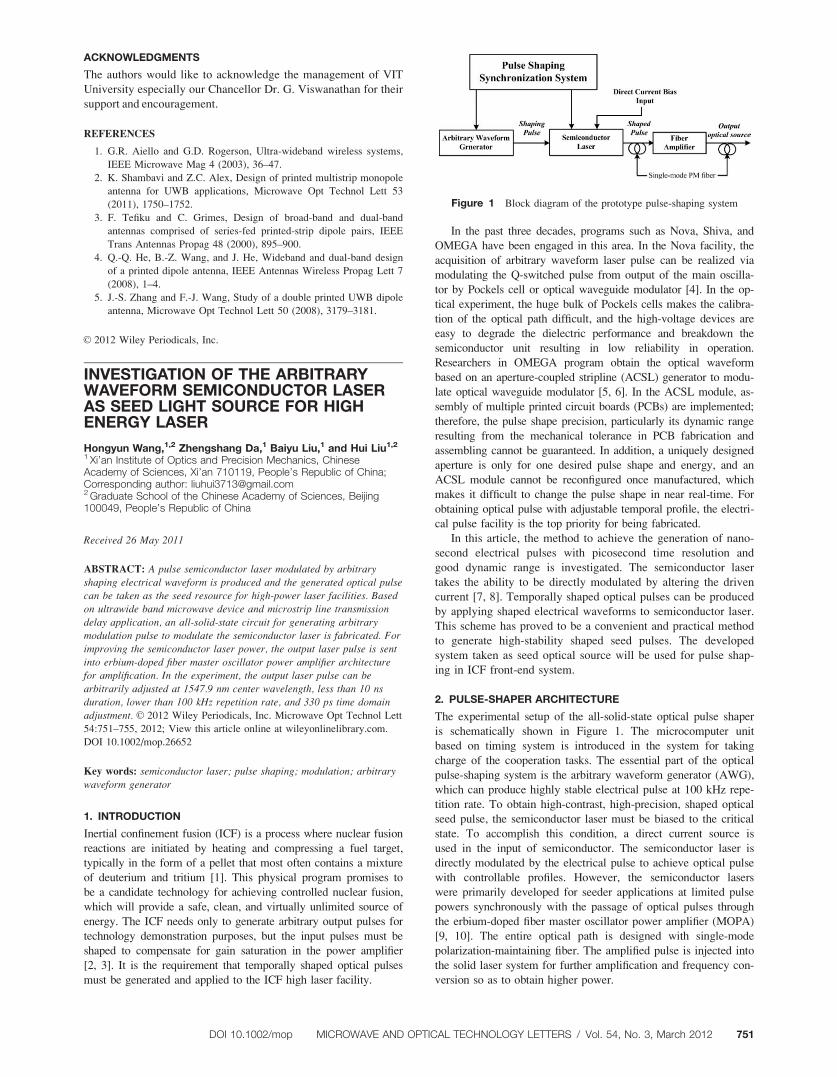
The experimental setup of the all-solid-state optical pulse shaper
is schematically shown in Figure 1. The microcomputer unit
based on timing system is introduced in the system for taking
charge of the cooperation tasks. The essential part of the optical
pulse-shaping system is the arbitrary waveform generator (AWG),
which can produce highly stable electrical pulse at 100 kHz repe-
tition rate. To obtain high-contrast, high-precision, shaped optical
seed pulse, the semiconductor laser must be biased to the critical
state. To accomplish this condition, a direct current source is
used in the input of semiconductor. The semiconductor laser is
directly modulated by the electrical pulse to achieve optical pulse
with controllable profiles. However, the semiconductor lasers
were primarily developed for seeder applications at limited pulse
powers synchronously with the passage of optical pulses through
the erbium-doped fiber master oscillator power amplifier (MOPA)
[9, 10]. The entire optical path is designed with single-mode
polarization-maintaining fiber. The amplified pulse is injected into
the solid laser system for further amplification and frequency con-
version so as to obtain higher power.
Figure 1 Block diagram of the prototype pulse-shaping system
DOI 10.1002/mop MICROWAVE AND OPTICAL TECHNOLOGY LETTERS / Vol. 54, No. 3, March 2012 751

3. ELECTRICAL SHAPING PULSE GENERATOR
3.1. The All-Solid-Stated CircuitThe proposed circuit is present in Figure 2; the transmission
lines used in microstrip line architecture consist of the pulse line
and the trigger line. The power GaAs FETs, which are com-
monly used in microwave amplifiers, are used in this project.
Each FET gate is fed with a direct current source to which a tap
resistor is connected, and the trigger pulse is transmitted through
the blocking capacitor directly to the gate. The gate bias V ini-
tially �8 V and the amplitude of the trigger pulse added to-
gether to decide the GaAs FET state. Originally, all the FETs
are biased in the off state because their cutoff voltage is nomi-
nally �2.2 V. To initiate operation, a trigger pulse generated
from avalanche transistor is launched on the trigger line and
propagates past each of the metal-semiconductor field effect
transistors (MESFETs), which has effect to make the gate-source
voltage exceed the cutoff voltage. Thus, a triggered voltage wave-
let with similar waveform but adverse polarity to the triggering
pulse is generated on the pulse line, and it travels to two opposite
directions. The wave traveling to the left termination is assimi-
lated by the resistor and the right traveling one becomes part of
the shaped pulse, which is being constructed from these wavelets.
The shaped pulse is built as shown in Figure 3. The first wave-
let becomes the rising edge of the initial shaped pulse and the last
one becomes the falling edge. The trigger line delay is 630 ps
between two FETs as compared to the 300 ps delay along the
pulse, and the temporal difference 330 ps is the designed time do-
main adjustment. Thus, after each wavelet is added to the shaped
pulse, it propagates entirely past the next FET, which is triggered
at such a time to add on the next part of the shaped pulse. In this
way, the pulse is assembled until the desired pulse shape has been
generated. At the end of shaping pulse output, the ripples from the
wavelet addition can be removed by pulse propagating through a
Figure 2 The unit pulse accumulating process
Figure 3 The final shaped pulse is constructed from scaled and
delayed replicas of the trigger pulse
Figure 4 Tapered line architecture. [Color figure can be viewed in the
online issue, which is available at wileyonlinelibrary.com]
Figure 5 The comparing of the fist unit pulse and the last one. [Color
figure can be viewed in the online issue, which is available at
wileyonlinelibrary.com]
Figure 6 Wavelength of semiconductor laser. [Color figure can be
viewed in the online issue, which is available at wileyonlinelibrary.com]
752 MICROWAVE AND OPTICAL TECHNOLOGY LETTERS / Vol. 54, No. 3, March 2012 DOI 10.1002/mop

DC blocking capacitor or a maximally linear phase low-pass filter.
The electrical pulse is applied on a semiconductor laser and the
desired optical pulse is obtained. The pulse shape is varied by set-
ting a bias voltage on each chain of FETs.
3.2. Transmission Line DesignThe design of the transmission lines is of critical importance to
any all-solid-state circuit. Microstrip is a type of electrical trans-
mission line, which can be fabricated using PCB technology,
and it is used to convey microwave-frequency signals. In this
study, the microstrip line is fabricated for propagating the trig-
ger pulse and the shaped pulse with ultrafast rising and falling
edges, respectively. It is a fact that the pulse attenuation in am-
plitude is introduced in the propagation process. Circuit losses
are introduced by allowing the effective dielectric constant in
the telegraph equation to have an imaginary component, which
can be related to the substrate’s loss tangent and the conductor’s
ohmic losses. So, the linearly tapered microstrip line (LTML) is
applied for compensating the trigger pulse attenuation [11, 12].
Figure 4 illustrates the top view of LTML architecture.
With the designed LTML in all-solid-state shaping circuit, we
set the first unit GaAs FET gate bias and the last one at the same
value, and two unit pluses are generated from the pulse line,
which is shown in Figure 5. Figure 5 demonstrates the triggered
pulse with the similar amplitude. However, the last unit pulse
becomes wider than the first one resulting from the pulse fre-
quency dissipation in pulse propagation. Therefore, the LTML
design has been definitely supported by experimental results.
4. SYSTEM PERFORMANCE AND ANALYSIS
4.1. The Characteristic of Input–OutputThe AWG is varied by setting a chain of bias voltage on GaAs
FETs gate. The temporal-shaped pulse generated from AWG is
taken as a current source for modulating the semiconductor
laser. In this study, we used a semiconductor laser at 1547.8 nm
central wavelength, which is shown in Figure 6, and the peak
power is 8 mW. There are two typical optical waveforms shown
in Figures 7 and 8. Figures marked (a) are the electrical pulse
and the (b) are the optical pulse output from the semiconductor
laser. Measurements are made by the LeCory oscillograph (40
GHz sampling frequency and 11 GHz bandwidth) and a photo
detector (40 GHz bandwidth). Figure 7(a) is a ladder pulse and
Figure 8(a) is a triangle pulse; Figures 7(b) and 8(b) are their
corresponding optical pulses, which have the same temporal pro-
file as the electrical ones. These figures illustrate that the shaped
optical pulses agree well with the electrical waveform with
excellent performance and predictability.
Comparing the electrical and optical pulses from (a) and (b),
we can observe that the glitch in electrical pulses is eliminated
when sending the pulses into the electro-optic waveguide modu-
lator. In the Fourier transform domain, the glitch is the high-fre-
quency components of the signal, and the modulator’s perform-
ance is viewed as a low-pass filter. The high-frequency
components of the electrical pulse cannot make response on the
waveguide modulator. Therefore, the optical pulse becomes
much smooth.
Figure 7 The ladder pulse. [Color figure can be viewed in the online issue, which is available at wileyonlinelibrary.com]
Figure 8 The triangle pulse. [Color figure can be viewed in the online issue, which is available at wileyonlinelibrary.com]
Figure 9 Square optical pulse is amplified in EDFA with aberrance
DOI 10.1002/mop MICROWAVE AND OPTICAL TECHNOLOGY LETTERS / Vol. 54, No. 3, March 2012 753
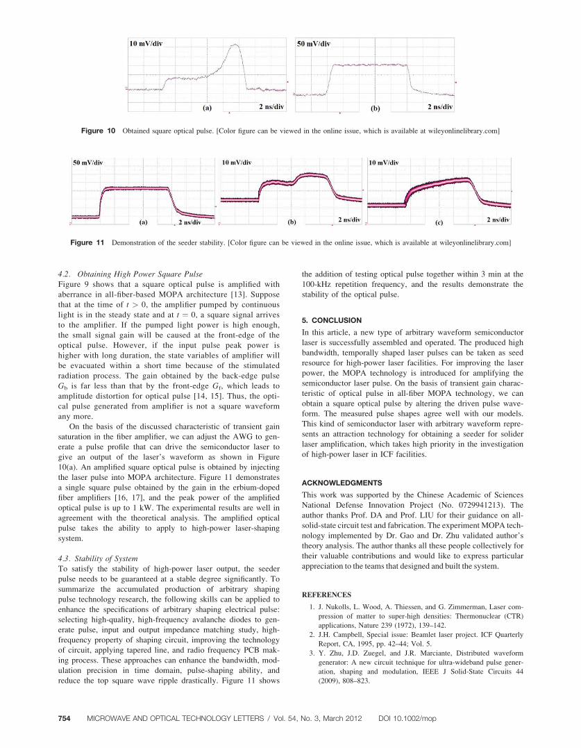
4.2. Obtaining High Power Square PulseFigure 9 shows that a square optical pulse is amplified with
aberrance in all-fiber-based MOPA architecture [13]. Suppose
that at the time of t > 0, the amplifier pumped by continuous
light is in the steady state and at t ¼ 0, a square signal arrives
to the amplifier. If the pumped light power is high enough,
the small signal gain will be caused at the front-edge of the
optical pulse. However, if the input pulse peak power is
higher with long duration, the state variables of amplifier will
be evacuated within a short time because of the stimulated
radiation process. The gain obtained by the back-edge pulse
Gb is far less than that by the front-edge Gf, which leads to
amplitude distortion for optical pulse [14, 15]. Thus, the opti-
cal pulse generated from amplifier is not a square waveform
any more.
On the basis of the discussed characteristic of transient gain
saturation in the fiber amplifier, we can adjust the AWG to gen-
erate a pulse profile that can drive the semiconductor laser to
give an output of the laser’s waveform as shown in Figure
10(a). An amplified square optical pulse is obtained by injecting
the laser pulse into MOPA architecture. Figure 11 demonstrates
a single square pulse obtained by the gain in the erbium-doped
fiber amplifiers [16, 17], and the peak power of the amplified
optical pulse is up to 1 kW. The experimental results are well in
agreement with the theoretical analysis. The amplified optical
pulse takes the ability to apply to high-power laser-shaping
system.
4.3. Stability of SystemTo satisfy the stability of high-power laser output, the seeder
pulse needs to be guaranteed at a stable degree significantly. To
summarize the accumulated production of arbitrary shaping
pulse technology research, the following skills can be applied to
enhance the specifications of arbitrary shaping electrical pulse:
selecting high-quality, high-frequency avalanche diodes to gen-
erate pulse, input and output impedance matching study, high-
frequency property of shaping circuit, improving the technology
of circuit, applying tapered line, and radio frequency PCB mak-
ing process. These approaches can enhance the bandwidth, mod-
ulation precision in time domain, pulse-shaping ability, and
reduce the top square wave ripple drastically. Figure 11 shows
the addition of testing optical pulse together within 3 min at the
100-kHz repetition frequency, and the results demonstrate the
stability of the optical pulse.
5. CONCLUSION
In this article, a new type of arbitrary waveform semiconductor
laser is successfully assembled and operated. The produced high
bandwidth, temporally shaped laser pulses can be taken as seed
resource for high-power laser facilities. For improving the laser
power, the MOPA technology is introduced for amplifying the
semiconductor laser pulse. On the basis of transient gain charac-
teristic of optical pulse in all-fiber MOPA technology, we can
obtain a square optical pulse by altering the driven pulse wave-
form. The measured pulse shapes agree well with our models.
This kind of semiconductor laser with arbitrary waveform repre-
sents an attraction technology for obtaining a seeder for solider
laser amplification, which takes high priority in the investigation
of high-power laser in ICF facilities.
ACKNOWLEDGMENTS
This work was supported by the Chinese Academic of Sciences
National Defense Innovation Project (No. 0729941213). The
author thanks Prof. DA and Prof. LIU for their guidance on all-
solid-state circuit test and fabrication. The experiment MOPA tech-
nology implemented by Dr. Gao and Dr. Zhu validated author’s
theory analysis. The author thanks all these people collectively for
their valuable contributions and would like to express particular
appreciation to the teams that designed and built the system.
REFERENCES
1. J. Nukolls, L. Wood, A. Thiessen, and G. Zimmerman, Laser com-
pression of matter to super-high densities: Thermonuclear (CTR)
applications, Nature 239 (1972), 139–142.
2. J.H. Campbell, Special issue: Beamlet laser project. ICF Quarterly
Report, CA, 1995, pp. 42–44; Vol. 5.
3. Y. Zhu, J.D. Zuegel, and J.R. Marciante, Distributed waveform
generator: A new circuit technique for ultra-wideband pulse gener-
ation, shaping and modulation, IEEE J Solid-State Circuits 44
(2009), 808–823.
Figure 10 Obtained square optical pulse. [Color figure can be viewed in the online issue, which is available at wileyonlinelibrary.com]
Figure 11 Demonstration of the seeder stability. [Color figure can be viewed in the online issue, which is available at wileyonlinelibrary.com]
754 MICROWAVE AND OPTICAL TECHNOLOGY LETTERS / Vol. 54, No. 3, March 2012 DOI 10.1002/mop

4. R.B. Wilcox, Photoconductive switch pulse-shaping device for
Nova master oscillator, Laser Part Beams 4 (1986), 141–143.
5. M.D. Skeldon, Optical pulse-shaping system based on an electro-
optic modulator driven by an aperture-coupled-stripline electrical-
waveform generator, Opt Soc Am 19 (2002), 2423–2426.
6. A.V. Okishev, M.D. Skeldon, R.L. Keck, et al., All-solid-state opti-
cal pulse shaper for the OMEGA laser fusion facility, Adv Solid
State Lasers Opt Soc Am 34 (2000), 112–115.
7. L. Wang, X.D. Lin, Z.M. Wu, et al., Current-driven state-bistability
and power-bistability in a DFB semiconductor laser subject to opti-
cal injection, Laser Phys 20 (2010), 1957–1960.
8. M.S. Alias, S. Shaari, and S.M. Mitani, Optimization of electro-op-
tical characteristics of GaAs-based oxide confinement VCSEL,
Laser Phys 20 (2010), 806–810.
9. N.Md. Yusoff, M.H. Abu Bakar, S.J. Sheih, et al., Gain-flattened
erbium-doped fiber amplifier with flexible selective band for optical
networks, Laser Phys 20 (2010), 1747–1751.
10. M. Li, J. Ma, L.Y. Tan, et al., Investigation of the irradiation effect
on erbium-doped fiber amplifiers composed by different density er-
bium-doped fibers, Laser Phys 19 (2009), 138–142.
11. H. Wu and A. Hajimiri. Silicon-based distributed voltage con-
trolled oscillators. IEEE J Solid-State Circuit 36 (2001), 493–502.
12. C.L. Edwards, M.L. Edwards, S. Cheng, R. Stilwell, and C.C.
Davis, A simplified analytic CAD model for linearly tapered
microstrip lines, IEEE MIT-S Int Microwave Symp Dig 2003, Phil-
delphia, PA, 2101–2104.
13. C.L. Edwards, M. Lee Edwards, S. Cheng, R.K. Stilwell, and C.C.
Davis, Simplified analytic CAD model for linearly tapered micro-
strip lines including losses, IEEE Trans Microwave Theory Tech
53 (2004).
14. A.V. Gulyaev and O.V. Tikhonova, Propagation of the ultrashort
laser pulses through the quantum nonlinear medium with resonant
properties, Laser Phys 20 (2010), 1051–1060.
15. S.N. Andreev, N. Il’ichev, K.N. Firsov, et al., Generation of an
electrical signal upon the interaction of laser radiation with water
surface, Laser Phys 17 (2007), 1041–1052.
16. E. Dessurvice, C.R. Giles, and J.R. Simpson,Gain dynamics of er-
bium-doped fiber amplifiers, Proc. SPIE Conference on Fiber Laser
Source and Amplifiers, 1171, 1989, pp.103–118.
17. C. Gao, S. Zhu, W. Zhao, Z.y. Cao, and Z. Yang,Eye-safe, high-
energy, single-mode all-fiber laser with widely tunable repetition
rate 7 (2009).
VC 2012 Wiley Periodicals, Inc.
DESIGN OF AN INDOOR REPEATERANTENNA WITH HIGH ISOLATION USINGMETAMATERIALS
Youngki Lee, Jeageun Ha, and Jaehoon ChoiDepartment of Electronics and Communications Engineering,Hanyang University, 17 Haengdang-dong, Seongdong-gu, Seoul133-791, Korea; Corresponding author: [email protected]
Received 26 May 2011
ABSTRACT: In this article, an innovative indoor repeater antennawith high isolation is proposed. The necessary impedance bandwidth isobtained using the coupling between the main and parasitic patches. Ahigh isolation between transmitting and receiving antennas is achievedusing metamaterial. The fabricated indoor repeater antenna has aVSWR less than 1.5, a gain higher than 9.6 dBi, and an isolationbetween the transmitting and receiving antennas greater than 80 dBover the WiBro band from 2.3 to 2.5 GHz. VC 2012 Wiley Periodicals,
Inc. Microwave Opt Technol Lett 54:755–761, 2012; View this article
online at wileyonlinelibrary.com. DOI 10.1002/mop.26651
Key words: microstrip patch antenna; indoor repeater antenna;metamaterial; isolation
1. INTRODUCTION
Repeaters have been widely used in wireless communication
systems to improve the service quality at the cell edges, in shad-
owed areas, and in buildings. The use of repeaters is a cost-
effective solution for extending coverage in areas with low sig-
nal levels. On-frequency repeaters [1–4] use frequency more
effectively; however, the strong coupling between the receiving
and transmitting antennas severely degrades the signal quality.
As the input and output frequencies are the same for a channel-
selective repeater, the requirement for antenna isolation becomes
critical. Excessive feedback from the transmitting antenna to the
receiving antenna causes magnitude and phase errors in the
Figure 1 Structure of the proposed indoor repeater antenna: (a) side view
of the repeater antenna, (b) top view of the repeater antenna, (c) top view of
the metamaterial unit cell, and (d) side view of the metamaterial cell
DOI 10.1002/mop MICROWAVE AND OPTICAL TECHNOLOGY LETTERS / Vol. 54, No. 3, March 2012 755