investigation of metal-assisted si etching for fabrication of nanoimprint lithography stamps
TRANSCRIPT

Technical report, IDE 1056, October 2010
Investigation of Metal-assisted Si Etching for Fabrication
of Nanoimprint Lithography Stamps
Thesis submitted to the
Halmstad University, Sweden
For the degree of Masters of Science
In
Electrical Engineering
by
Ksenia Anokhina
Division of Solid State Physics
Department of Physics Lund University
School of Information Science, Computer and
Electrical Engineering
Halmstad University
Sweden 2010


Investigation of Metal-assisted Si Etching for
Fabrication of Nanoimprint Lithography Stamps
Ksenia Anokhina
Master Thesis for the Degree of Master of Science with a major in Electrical
Engineering
Division of Solid State Physics
Department of Physics Lund University
School of Information Science, Computer and
Electrical Engineering
Halmstad University
Sweden 2010


This diploma work is dedicated to my family and friends


ACKNOWLEDGEMENTS
This diploma work could not be done without the help given me by the people at the
Division of Solid State Physics at Lund University and School of Information Science, Computer
and Electrical Engineering at Halmstad University. I would like to show my gratitude to many
persons. Hereby I mention only a few of them.
I am very much obliged to both my supervisors, Ivan Maximov and Håkan Pettersson. I
am very thankful for the opportunity to work under their supervision. I want to express special
thanks to Ivan Maximov for giving me immense knowledge and great experience. I am grateful
for his suggestions, study guidance throughout the process of writing the diploma thesis. I would
like to acknowledge Håkan Pettersson and my teacher Lars Landin for giving me the opportunity
to do this work at Lund University. Special thanks to Mariusz Graczyk for the unwearied support
and help during my work. I would be glad to call him my third supervisor. I appreciate Anders
Kvennefors for inspiring me with cheerfulness, giving advice and teaching me how to operate
different machines. I would also like to thank Babak Heidari (Obducat AB), Gang Luo, Bengt
Meuller, and Maria Messing for their cooperation in different processing steps of my work.
Special thanks to Håkan Lapovski and George Rydnemalm for helping in the lab. I express
thanks to Dmitry Suyatin for supporting me and giving useful advice.
Finally I would like to thank my family and friends for great support during my work on
the present diploma thesis.


ABSTRACT
This diploma thesis deals with the investigation of the metal-assisted catalytic etching
(MaCE) of Si. One of the main goals is to study stamps fabrication for nanoimprint lithography
using MaCE.
A formation of nanoporous silicon (PSi), Si nanowires (SiNWs) and three-dimensional
nanostructures in Si by MaCE is demonstrated. For this purpose optical lithography, electron
beam lithography (EBL), shadow mask evaporation and aerosol nanoparticles deposition
techniques have been utilized. The etching rate and surface morphology of Si (with Au lift-off
films as a catalyst) as functions of time and concentrations of chemicals are measured in the
current diploma work using optical microscope and scanning electron microscopy (SEM). In the
current thesis it is shown that Si structures with sub-150 nm lateral sizes, high aspect ratio (up to
1:21), well-defined shapes, and various complexity can be easily fabricated by means of MaCE
process.


CONTENT
1. INTRODUCTION .............................................................................................................................................. 1
1.1. Metal-assisted chemical etching of Si............................................................................ 2
1.2. Investigation and applications of MaCE ........................................................................ 3
1.3. Nanoimprint lithography and methods of stamp fabrication .......................................... 9
1.3.1. Optimized electron beam lithography (EBL) and lift-off pattering of a Cr mask ... 10
1.3.2. Aerosol deposition of W particles ........................................................................ 10
1.3.3. Direct stamp fabrication using HSQ ..................................................................... 10
1.3.4. Metal-assisted chemical etching of Si .................................................................. 11
2. EXPERIMENTAL PART............................................................................................................................ 13
2.1. Experimental details.................................................................................................... 13
2.2. Formation of Si nanowires using shadow gold mask ................................................... 15
2.3. Nanoporous Si structures produced by MaCE ............................................................. 17
2.4. Study of kinetics of the MaCE process ........................................................................ 20
2.5. NIL stamps fabrication and imprint experiments ......................................................... 27
CONCLUSIONS ...................................................................................................................................................... 31
APPENDIX A Process steps of the metal-assisted Si etching................................................................. 33
APPENDIX B Fabrication of the Si nanowires using the shadow mask technique ........................ 34
APPENDIX C Production of the porous Si using the aerosol particles technique .......................... 35
APPENDIX D Process steps of the sample preparation using the optical lithography ................. 36
APPENDIX E Nanoimprint stamp fabrication using the electron beam lithography .................... 38
APPENDIX F Process steps of the nanoimprint lithography .................................................................. 39
REFERENCES ......................................................................................................................................................... 41


1
INTRODUCTION
These days, high-aspect ratio silicon structures are attracting interest due to their potential
application in broad areas ranging from electronics, photonics, and renewable energy to
biomedical sensing. There have been attempts to create new low-dimensional silicon
nanostructures, including Si nanowires, porous silicon, and related nanodevices. Silicon
nanowires (SiNWs), for example, are very attractive nanostructures because of their unique one-
dimensional nature and associated electrical, mechanical, and thermal properties. Currently,
SiNWs have been successfully implemented in solar cells, chemical sensors and field-effect
transistors. Porous silicon (PSi) is widely employed in applications such as silicon-based
optoelectronics, photonic crystals, optical filters, membranes, and molecular sieves. Interest in
PSi is explained due to the large surface-to-volume ratio.
There are a number of techniques to produce nanostructures in Si. Standard fabrication
techniques include wet chemical methods utilizing both acids and bases and dry chemical
methods such as ion etching and deep reactive ion etching. These techniques have two
limitations: complex 3D shapes are difficult to produce and it is very hard to maintain high
aspect ratio structures with varying degrees of complexity as feature sizes shrink into the
nanoscale.
SiNWs are produced by different methods such as laser ablation, thermal evaporation,
chemical vapor deposition, molecular beam epitaxy, chemical etching, and solution growth.
Nevertheless, controllable and repeatable fabrication of SiNWs arrays is still a problem.
PSi is usually produced by anodic etching, with and without illumination, by chemical
etching, and by photochemical etching. The last two techniques are used without external bias.
Chemical etching is usually slow, non-reproducible, and unreliable.
In the current diploma work, an alternative “top-down” approach, metal-assisted wet-
chemical Si etching (MaCE) [1-4], is considered as a promising solution to obtain high aspect
ratio nanostructures with well-defined shapes, and various complexity. The named approach is
also defined as a promising solution to achieve aligned SiNWs with control of the diameter,
length, spacing and density, and to create the PSi with controllable sizes and density of pores.
There is an increasing interest in nanoimprint lithography (NIL) due to its capability to
produce sub-10 nm features, process simplicity, high throughput and low cost. One of the main
aims of the diploma work is to study fabrication of NIL stamps using MaCE. The resolution and
quality of nanoimprint is determined entirely by the stamp so its fabrication is of tremendous
importance for NIL-based technology. In the present diploma thesis it is demonstrated that the
negative Si stamp comprising of sub-150 nm structures with well-defined shapes and various
complexities can be fabricated using metal-assisted catalytic Si etching.

2
1.1. Metal-assisted chemical etching of Si
Metal-assisted chemical etching (MaCE) is an alternative to the dry etching method. This
is a highly anisotropic process. MaCE has recently been applied to fabrication of high aspect
ratio SiNWs [4-8], three-dimensional, well-defined nanostructures [9-12] and PSi [3, 13-16]. In
MaCE, a metal catalyst such as Au, Pt, or Ag is deposited onto a silicon surface as either
nanoparticles or a discontinuous thin film that locally increases dissolution of silicon in an etch
solution of hydrofluoric acid (HF) and hydrogen peroxide (H2O2). A simplified schematic of the
MaCE process is illustrated in Fig. 1.1.
Metal pattern
Etching in a diluted HF/
H2O2 solution
Si
Si
Si
a)
b)
c)
Figure 1.1. Schematic illustration of the metal-assisted chemical etching of Si.
The process begins with a metal patterning on the Si substrate (Fig. 1.1b). The sample is
then immersed into an etching solution, which typically consists of diluted hydrofluoric
acid/hydrogen peroxide (HF / H2O2). Catalytic etching of the Si substrate under the metal layer
results in “sinking” of the metal into the substrate (Fig. 1.1c).
HF/H2O2
Si
Au e-
e-
e-
HF/H2O2
Si
Au e-
e-
e-
Figure 1.2. Schematic illustration of the autonomous Au particle movement in bulk Si.

3
The metal-assisted Si etching process is described as a catalytic conversion of chemical
free energy into propulsive mechanical power [1]. And it could be explained in the following
way (Fig. 1.2).
In the current work Au was used as a catalytic metal. Therefore the etching process
should be considered for the case of a Au particle. It has been suggested that the surface of a Au
particle facing the etching solution acts as the cathode [2-4], which catalyzes H2O2 reduction,
consuming H and electrons (e-). It could be described by the following reactions:
Cathode (Au):
H2O2 + 2H+ + 2e
- → 2H2O
2H+ + 2e
- → H2
The surface of the Au particle facing the Si works as the anode and it catalyzes Si
oxidation, generating H and e-, which is described as:
Anode (Si):
Si + 2H2O → SiO2 + 4H+ + 4e
-
SiO2 + 6HF → H2SiF6 + 2H2O
Si + 4HF → SiF4 + 4H+ + 4e
-
A potential difference appears between the cathode and the anode. Electrons flow from
the anode to the cathode. A local current flows in the opposite direction, from the cathode to the
anode.
The overall spontaneous power-generating reaction could be written in the following
way:
Si + 2H2O2 + 6HF → H2SiF6 + 2H2O +H2
So the etching process is localized in the regions covered by Au. Thus, the etching of Si
under the Au-particle results in its “sinking” into the substrate.
1.2. Investigation and applications of MaCE
A number of publications are related to the formation of nanoporous silicon, Si nanowires
and three-dimensional nanostructures in Si by the metal-assisted catalytic etching.
According to the literature (see below) metal-assisted Si etching depends on several
parameters, for example:
the type of deposited metal (Pt, Ag, Au, etc.)
the dopant type and doping level (n- or p-type)
etching time, temperature of etching and ambient illumination
concentration of etchants (HF, H2O2, dilution)

4
wafer orientation (<100>, <111>, <110>, <113>)
morphology of the metal film (single particles, discontinuous or continuous film)
Therefore Si structures with different morphologies and properties can be produced by
varying these parameters.
K. Peng et al. [1] has shown a dependence of the morphology of etched samples on the
wafer crystal orientation (Fig. 1.3). They demonstrated that Si (100) wafer shows large area
aligned SiNW arrays perpendicular to the Si surface after etching process. P-type Si (111) wafer
gives both vertical and slanting aligned SiNW arrays. P-type (110) and n-type (113) wafers
produce SiNWs at the angle or slanted to the Si surface. It characterizes the MaCE as an
anisotropic process. Also they have shown that the etching rate of Si increases with increasing
concentrations of HF and H2O2.
Figure 1.3. Cross-sectional SEM images of Ag particle-coated Si wafers after etching in aqueous
HF/H2O2 solution for 30 min showing aligned Si nanowire arrays produced on: a) p-type 7–14Ω
cm Si (100) wafer, b) p-type 5x10⁻³
Ω cm Si (111) wafer, c) p-type 4–7Ω cm Si (110) wafer, and
d) n-type 4–7Ω cm Si (113) wafer. Adopted from [1].
P.W. Bohn et al. [3] studied the dependence of the MaCE process on the type of
deposited metal (Fig. 1.4). Their results showed that a much rougher and deeper structure is
produced on Pt-coated Si than on Au-coated Si. The authors also found that PSi produced with Pt
as a catalyst resulted in stronger photoluminescence (PL) than PSi made with Au. They
concluded that the stronger PL can be seen from the Pt-coated area for the p+-wafer, while the

5
uncoated area produces stronger photoluminescence in the p- sample. Strong PL-signal is also
acquired from the Pt-coated areas on n+ silicon.
a) b)
Figure 1.4. SEM images of (a) Au-coated Si (100) after etching in HF/H2O2 for 30 s and (b) Pt-
coated Si (100) after etching in HF/H2O2 for 30 s. Adopted from [3].
An in-depth study of MaCE by J. Teva et al. [17] has demonstrated that for a given gold
thickness the etch rate of (111) Si wafers is lower than for (100) Si wafers. For both types of
wafers, the maximum etch rate is obtained when the gold film is about 40 – 50 nm thick (Fig.
1.5).
Figure 1.5. Measured etch rate ɛr versus the deposited gold thickness te for (111) and (110) Si
wafers. Adopted from [17].
X. Duan et al. [5] demonstrated that the etch rate increases with increase of the H2O2
concentration and reaction time (Fig. 1.6).
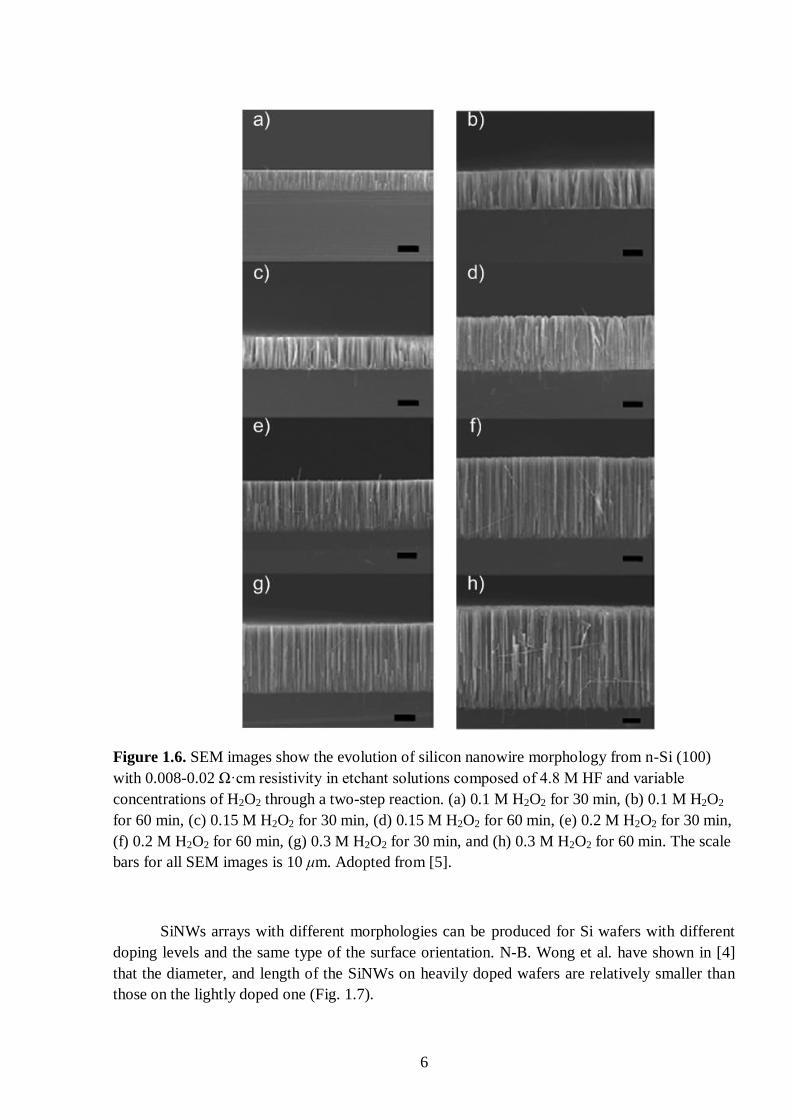
6
Figure 1.6. SEM images show the evolution of silicon nanowire morphology from n-Si (100)
with 0.008-0.02 Ω·cm resistivity in etchant solutions composed of 4.8 M HF and variable
concentrations of H2O2 through a two-step reaction. (a) 0.1 M H2O2 for 30 min, (b) 0.1 M H2O2
for 60 min, (c) 0.15 M H2O2 for 30 min, (d) 0.15 M H2O2 for 60 min, (e) 0.2 M H2O2 for 30 min,
(f) 0.2 M H2O2 for 60 min, (g) 0.3 M H2O2 for 30 min, and (h) 0.3 M H2O2 for 60 min. The scale
bars for all SEM images is 10 μm. Adopted from [5].
SiNWs arrays with different morphologies can be produced for Si wafers with different
doping levels and the same type of the surface orientation. N-B. Wong et al. have shown in [4]
that the diameter, and length of the SiNWs on heavily doped wafers are relatively smaller than
those on the lightly doped one (Fig. 1.7).

7
Figure 1.7. SEM images from p-Si (111) substrates: (a, b, c) from the lightly doped wafer and
(d, e, f) from the heavily doped wafer. Insets: corresponding top views in high magnification.
Adopted from [4].
Figure 1.8. Schematic of steps involved in the fabrication of MaCE patterns of (a) porous silicon
from discrete nanoparticles, (b) silicon nanowires from discontinuous metal films or high density
nanoparticle layers, and (c) 3D silicon nanostructures from slightly discontinuous metal films.
Adopted from [12].
G. Fedorov et al. [12] have shown the influence of the metal film morphology on the
morphology of the Si structures after the etching process (Fig. 1.8).
8
The authors used a thin layer of amorphous carbon formed using electron beam induced
deposition (aC EBID) for fabrication of either PSi (deposition of Au particles, Fig. 1.8a), or
SiNWs (Au film should be discontinuous, Fig. 1.8b), or 3D silicon nanostructures (continuous
Au film, Fig. 1.8c).
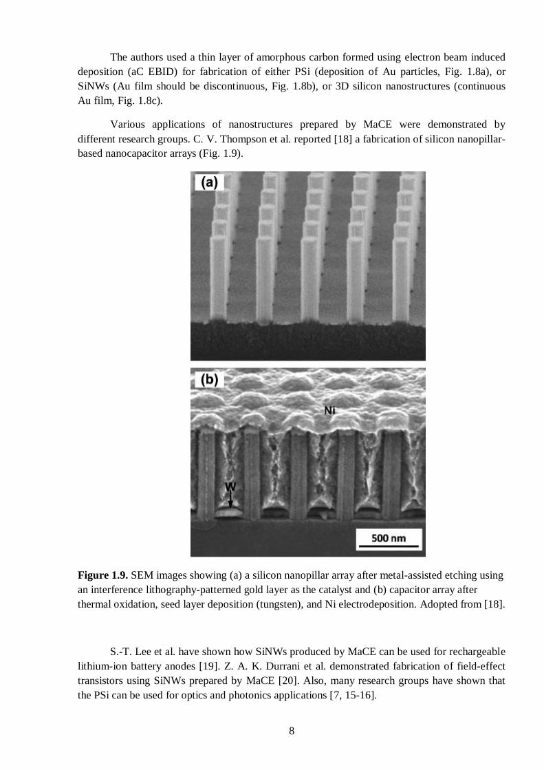
Various applications of nanostructures prepared by MaCE were demonstrated by
different research groups. C. V. Thompson et al. reported [18] a fabrication of silicon nanopillar-
based nanocapacitor arrays (Fig. 1.9).
Figure 1.9. SEM images showing (a) a silicon nanopillar array after metal-assisted etching using
an interference lithography-patterned gold layer as the catalyst and (b) capacitor array after
thermal oxidation, seed layer deposition (tungsten), and Ni electrodeposition. Adopted from [18].
S.-T. Lee et al. have shown how SiNWs produced by MaCE can be used for rechargeable
lithium-ion battery anodes [19]. Z. A. K. Durrani et al. demonstrated fabrication of field-effect
transistors using SiNWs prepared by MaCE [20]. Also, many research groups have shown that
the PSi can be used for optics and photonics applications [7, 15-16].

9
1.3. Nanoimprint lithography and methods of stamp fabrication
Nanoimprint lithography is a parallel lithography method of direct transfer of
prefabricated stamp patterns’ onto a resist spun on a substrate. Nanoimprint lithography
combines low cost, high throughput and nanometer-scale resolution. Sub-10 nm features can be
produced with this technique. Nanoimprint lithography allows a patterning of wafers up to 6
inches in diameter.
There are two main types of NIL:
thermal NIL
UV NIL
In this diploma work thermal NIL has been used. The basic process is illustrated in Fig.
1.10.
Double
resist
system
Si
Si
Preasure and temperature
1. matching 2. imprinting 3. separation
stamp
Figure 1.10. Schematic illustration of the thermal nanoimprint process.
The main steps of NIL are:
fabrication of a stamp
deposition of a resist on wafer by spin-coating
matching of the stamp and prepared wafer
heating of the stamp and the substrate up above the glass transition
temperature of the resist
pressing the stamp against the substrate with certain pressure
imprinting of stamp structures onto a resist
lowering the temperature below glass transition temperature and removing the
stamp
removing the residual layer by O2 plasma ashing
deposition of a metal layer
lift-off process to remove resist and unwanted metal
Thermal nanoimprint lithography is also called hot embossing lithography.

10
Since the stamp pattern transfers onto a resist over the substrate it is impossible to obtain
a quality and resolution of the imprinted pattern better than the corresponding characteristics of
the stamp pattern. Thus a stamp fabrication method should be chosen carefully.
Various methods for the stamp fabrication have been developed [21-25] In this diploma
work only few of them are considered:
1) Optimized electron beam lithography (EBL) and lift-off pattering of a Cr mask
[21]
2) Aerosol deposition of W particles [21]
3) Direct stamp fabrication using HSQ [22]
4) Metal-assisted Si etching
1.3.1. Optimized electron beam lithography (EBL) and lift-off pattering of a Cr
mask
This method of stamp fabrication is one of the commonly used ones. It starts with thermal
oxidation of Si wafer to form 200-500 nm thick silicon oxide layer. The following process steps
include cleaning of the SiO2 surface by conventional organic solvents, spin-coating of a double
layer e-beam resist followed by exposure in an EBL machine. After development of the resist
and thermal evaporation of Cr mask, lift-off is performed to form metal mask. The NIL stamp
features are transferred from the Cr mask into the silicon oxide by reactive ion etching step.
1.3.2. Aerosol deposition of W particles
The NIL stamps can be produced using direct deposition of W aerosol particles onto the
thermally oxidized Si surface. The aerosols are used as etch mask in a subsequent RIE process
step and allow formation of SiO2 columns with the size of the W aerosols (about 20 to 100 nm).
This approach is very simple and fast, since the EBL exposure is not used, but it is difficult to
control deposition of the aerosols: the methods results in randomly formed columns in the
stamps.
1.3.3. Direct stamp fabrication using HSQ
This method of fabrication of NIL stamps is based on newly developed negative e-beam
resist hydrogen silsequioxane (HSQ). A number of research groups have shown that the resist
had very small line width fluctuations compared to commonly used positive e-beam resists
(PMMA and ZEP520). Line widths down to 10 nm were demonstrated. Biggest advantage of
HSQ for fabrication of NIL stamps is its ability to convert to SiOx after exposure, development
and annealing.

11
1.3.4. Metal-assisted chemical etching of Si
The MaCE process has been described above. It is important to note that a “negative”
stamp for nanoimprint lithography is formed by means of this technique. The main difference
between “positive” and “negative” stamp is that the percentage of the raised areas is high for a
“negative” stamp and small for a “positive” stamp (Fig. 1.11).
b)a)
Figure 1.11. Positive (a) and negative (b) stamps for the nanoimprint lithography.

12

13
2. EXPERIMENTAL PART
Different techniques were utilized to form Au catalysts for studies of metal-assisted
etching of Si. These are shadow mask evaporation, aerosol particles deposition, optical
lithography, and electron beam lithography (EBL). The main goal of the present diploma work
is investigation of the MaCE process. For this purpose shadow mask evaporation and aerosol
particles deposition were tested due to the simplicity of sample preparation, low cost and process
purity. These techniques are also fast and resist free, which is very important when many
experiments have to be performed. Fabrication methods to make Si nanowires and porous Si
nanostructures have been developed during the study of MaCE using aerosol particles and
shadow mask techniques.
Advantages of contact optical lithography are low cost, high throughput and moderately
high resolution (limited by the wavelength of light). This technique was utilized to prepare the
samples for in-depth studies of MaCE such as measuring etching rates and surface morphology
of Si as functions of time and concentrations of chemicals (with Au lift-off films used as a
catalyst).
Electron beam lithography is a high cost technique with low throughput. The main
advantage of EBL is a very high resolution. Sub-10 nm structures can be obtained using this
technique. Due to this the EBL was used only for the nanoimprint stamps fabrication.
2.1. Experimental details
One or two inch n-type Si (100) wafers with resistivity of 10 Ω∙cm were used as
substrates in all experiments.
Au was used as a metal catalyst in the current work. The thickness of the Au film was 20
nm and the evaporation rate was about 2.1 Å/s in all experiments. For evaporation of the Au film
two systems were used. The evaporator Pfeiffer Classic 500 was utilized to produce
discontinuous gold film. The evaporator AVAC was used to obtain a continuous gold film.
Aerosol gold particles were deposited using the aerosol nanoparticle system including
both an evaporation/condensation source and the spark discharge generator Palas GfG 1000 [26-
27]. Firstly, the size of the particles was selected using a differential mobility analyzer (DMA).
The particles were deposited onto the substrate in an electric field. The nominal diameter of the
particles was 70-80 nm. The particle density was about 6x108 cm
-2. The carrier gas was purified
nitrogen throughout the aerosol process [appendix C].
A Karl Süss MJB 3 mask aligner was employed for the optical lithography patterning.
The exposure was done during 5 s (11.5-12 mW/cm2) with vacuum contact.
Prior to deposition of resists, the wafers were annealed at 180°C for 3 hours in an oven. A
double layer resist system was used. After the deposition of the bottom layer (positive resist
LOR 3A) by spinning, the wafers were baked at 160°C for 20 min in an oven. Wafers were

14
additionally baked at 115°C for 1.5 min using a hot plate after the deposition of the second layer
(positive resist S1813). Following the exposure, the samples were developed in MF319 for 90 s,
wafers were rinsed in deionized water and blown dry with nitrogen. The resist residuals were
ashed in O2 plasma for 8 s using a microwave asher (New PlasmaPreen). After the thermal
evaporation of the Au film it was lifted-off in a Remover 1165 [appendix D].
For the EBL patterning, we employed a Raith 150 (Raith GmbH, Germany) equipped
with a thermal field emission cathode and a laser interferometer stage. The EBL system was
operated at 20 kV with an electron probe current of 36 pA. Different structures (including single
pixel lines, single pixel dots and grids with different geometry) were exposed in a writing field of
200 x 200 μm2 with step size 0.01 μm and different doses.
The wafers were cleaned in acetone and isopropanol followed by the spin-coating of the
polymethylmethacrylate (PMMA 950 A5) resist. Afterwards the wafers were baked at 160°C for
10 min using a hot-plate.
Following the EBL exposure, the resist was developed in a mixture of
methylisobutylketone / isopropanol (MIBK/ IPA 1:3) for 1 min, the wafers were rinsed in
isopropanol and blown dry with nitrogen. Immediately after development, the resist residuals
were ashed in O2 plasma for 8 s. Following the oxygen plasma ashing the Au film was thermally
evaporated in the evaporator AVAC and lifted-off in Remover 1165 heated at 60°C using a hot
plate [appendix E].
The etching was performed at room temperature and ambient illumination. Etch solutions
were prepared directly before the etching process [appendix A].
Clean, wide and low Teflon beakers were used as vessels for the solution of hydrofluoric
acid, hydrogen peroxide and deionized water (HF/H2O2/H2O). Firstly, a necessary amount of
deionized water is poured into the baker. Then aqueous hydrogen peroxide (H2O2) is added to
deionized water. The final step of the etch solution preparation was adding the aqueous
hydrofluoric acid (HF) to the mixture of H2O2/H2O. The chemicals, 48% hydrofluoric acid and
30% hydrogen peroxide, were supplied by Merck (Germany).
Two types of etch solutions were primarily tested: a strong solution (“solution S”) and a
week solution (“solution W”). Hydrofluoric acid, hydrogen peroxide and deionized water were
taken in proportions of 4 ml : 1 ml : 8 ml (48% HF : 30% H2O2 : H2O) for the “solution S” and in
proportions of 4 ml : 1 ml : 40 ml (48% HF : 30% H2O2 : H2O) for the “solution W”.
Silicon samples with Au-pattern were placed in the beaker containing the etchant for
different times, ranging from 30 s to 10 min. After the etching is completed the samples were
removed carefully from the beaker using Teflon tweezers. Due to hydrophobic properties of the
sample surface after etching, normally no solution is present on the samples after removal from
the etchant. Following the samples were rinsed in deionized water for at least 60 s. The samples
were placed on a cleanroom cloth and blown dry with a nitrogen gun.
The surface morphology of the etched samples was characterized using optical
microscopy (Axio Imager A1m, Carl Zeiss) in both bright and dark fields.

15
Scanning electron microscope (SEM) LEO/ZEISS 1560 was used for more detailed
surface studies of the etched samples. Typically the accelerating voltage of the SEM was about
15 kV, and the work distance was varying from 3 to 6 mm. The SEM was used to characterize
the surface morphology both in plane and cross sections. For better imaging conditions, the
etched samples were sometimes tilted 30° or 45°.
For the imprint experiments, the 6-inch nanoimprinter (Obducat AB) was used. Typical
thermal imprint conditions were 200°C and 50 bar for the imprint temperature and pressure,
respectively. Details of the NIL experiments are given in appendix F.
2.2. Formation of Si nanowires using shadow gold mask
As discussed previously, SiNWs can be easily produced by MaCE [appendix B]. The 20
nm thick Au film was evaporated through a shadow mask. Advantages of the shadow mask
technique are mentioned above. A metal film should be discontinuous for SiNWs growth . The
best Au film morphology was obtained using the evaporator Pfeiffer (Fig. 2.1).
To obtain SiNWs the “solution S” was used and the etching time was 5 min in all
experiments. Two groups of samples were prepared. The first group was with native oxide and
the second group was without native oxide. The second group of samples was etched in diluted
hydrofluoric acid (1:100) for 30 s to remove the native oxide.
MaCE of the two groups of samples showed no difference in the morphology of the
etched Si. Thus, removal of the native oxide was not necessary.
Figure 2.1. Morphology of the Au film with thickness of 20 nm obtained using Pfeiffer
evaporator (top view). Evaporation rate is about 2.1 Å/s.
During the MaCE process arrays of SiNWs appeared. The produced nanowires were
about 25 nm in diameter and 6.8 μm long in case of the samples without native oxide (Fig. 2.2).

16
a)
b)
Figure 2.2. SEM images showing SiNWs resulting from metal-assisted etching in a solution of
HF : H2O2 : H2O (4 ml : 1 ml : 8 ml) for 5 min (cross-section). (a) large-field view and (b)
detailed view revealing SiNWs dimensions of about 25 nm in diameter and 6.8 μm length.
The shadow mask technique has two main disadvantages. It has a very low resolution and
it does not provide a close fit between the shadow mask and the substrate (Fig.2.3) and the gap
can affect the shape of the deposited material. As a result, pattern edges are not well-defined.
SEM images of etched samples prepared by the shadow mask technique are shown in Fig. 2.4.
These images demonstrate that it is impossible to deposit a material layer with uniform thickness
and well-defined edges using the shadow mask technique.
material
Shadow
mask
Si
d
Figure 2.3. Schematic illustrating the process of material deposition using the shadow mask
technique.

17
Arrays of
nanowires
Edge between
the pattern and
uncovered Si
surface
Unetched Si
surface
Unetched
Si surfaceEtched Si
surface (arrays
of nanowires) Cleavage
Cross-
section
Edge between the pattern and
uncovered Si surface
Figure 2.4. SEM images of top-view (left) and cross-section (right) of etched Si at the border of
the shadow mask. Variation of Au thickness results in poor definition of the edge.
It was demonstrated that SiNWs can be easily produced by the MaCE process using the
shadow mask technique. It is possible to control length of SiNWs by changing the etching time
and the etch solution. It was also demonstrated that the removal of the native oxide is not
necessary.
2.3. Nanoporous Si structures produced by MaCE
Two alternative methods showed that nanoporous Si structures can be produced by the
metal-assisted chemical etching. The well-defined nanometer-sized gold particles were
synthesized both by the aerosol technique (Fig. 2.5) and electron beam lithography.
Figure 2.5. Top-view SEM images of aerosol particles (nominal size is about 70-80 nm, density
is about 6x108 cm
-2) deposited by the aerosol nanoparticle system.
The aerosol particles deposition technique has the same advantages as the shadow mask
evaporation technique. The aerosol particles deposition technique also allows control over the
density, shape and size of the particles. The aerosol nanoparticle system includes both a spark
discharge generator (SDG) and an evaporation/condensation source (Fig. 2.6) [26-27]. The
material is evaporated, then cooled to form condensates of nanoparticles in the

18
evaporation/condensation source. Particles of sizes ranging from 10 nm to about 100 nm can be
produced. There is a commercial SDG (Palas GfG 1000) along with the high temperature
furnace. The source can be selected just by rerouting the carrier gas.
The aerosols are transported by the carrier gas through a bipolar charger after being
generated. A differential mobility analyzer (DMA) is used to make a size selection. Subsequently
the particle number concentration is measured by an electrometer. The deposition is done in the
electrostatic precipitator.
Figure 2.6. Schematic of the aerosol nanoparticle system.
Directly after the deposition of the Au particles, the samples were etched in “solution S”
for 5 min. (Fig. 2.7a, b). Au particles are expected to “sink” strictly orthogonal to the surface of a
(100)-oriented Si substrate during the etching process. Figures 2.7a-b indicate unexpected
particle displacements along the surface (in arbitrary directions). To improve the adhesion of Au
particles to the Si surface the wafers were annealed at 350°C for 30 min before the etching
process. The etching results did not show any effects of annealing (Fig. 2.7c-d).
Electron beam lithography allows creation of ordered arrays of nanometer-sized gold
particles in contrast to the aerosol particles technique. Single pixel dots (SPDs) were exposed in
a writing field of 200 x 200 μm2 with a step size of 0.01 μm and dwell time of 281 μs. The size
of the SPDs was about 80 nm. “Solution S” and etch time of 5 min were chosen as etch
parameters. Figure 2.8 illustrates particles displacements along the surface during the etching
process.

19
a) b)
c) d)
Figure 2.7. SEM images illustrating metal-assisted etched nanoporous Si structures in a solution
of HF : H2O2 : H2O (4 ml : 1 ml : 8 ml) for 5 min (top view). (a) large-field view and (b) detailed
view of the sample etched without annealing. (c) large-field view and (d) detailed view of the
annealed sample at 350°C for 30 min.
Figure 2.8. SEM images illustrating metal-assisted etched nanoporous Si structures in a solution
of HF : H2O2 : H2O (4 ml : 1 ml : 8 ml) for 5 min (top view).
It was shown that the etching process cannot be controlled for Au structures with a lateral
size less than 80 nm due to the insufficient adhesion of Au to the Si surface. However,
nanoporous Si structures can simply be produced both by the aerosol particles technique and
electron beam lithography. These techniques allow control over the density, shape and size of the
particles. Therefore, the porosity of the etched Si can also be controlled. Another advantage is
that particles with a nominal diameter below 20–30 nm can be produced by both techniques.

20
A comparison of samples nanoporous Si structures prepared by the two different
techniques has not shown a considerable difference in the morphology of the etched samples.
Thus aerosol particles technique is much more attractive for the fabrication of the PSi than EBL
due to the complicity of the process of the latter.
2.4. Study of kinetics of the MaCE process
Several experiments were performed with samples made by optical lithography [appendix
D] for a study of the MaCE process. Advantages of optical contact lithography were described
above.
Samples were etched in “solution W” for various times (30 s – 10 min) to measure the
time dependence of the etch depth. Figure 2.9 shows SEM images of the etched samples for
different etching times (the etch depth is in the range of 107 nm – 2.9 μm). The images
demonstrate that mesa structures with well-defined shapes formed during the etching process.
The morphology of the formed structures characterizes the metal-assisted etching as a high
anisotropy process. Due to the discontinuity of the Au film (Fig. 2.10) the etching process results
in formation of the SiNWs.
a)
107 nm
b)
274 nm
c)
758 nm
d)
1.15 µm

21
e)
1.7 µm
f)
2.9 µm
Figure 2.9. SEM images illustrating cross-sections of the etched samples made by optical
lithography and subsequent O2 plasma ashing. The etch solution is a mixture of HF : H2O2 : H2O
(4 ml : 1 ml : 40 ml). (a) etching time (tetch) =30 s, etch depth (hetch) = 107 nm, (b) tetch=1 min,
hetch=274 nm, (c) tetch=3 min, hetch=758 nm, (d) tetch=5 min, hetch=1.15 μm, (e) tetch=7 min,
hetch=1.7 μm, (f) tetch=10 min, hetch=2.9 μm.
Figure 2.10. Morphology of the Au film with thickness of 20 nm obtained by the Pfeiffer
evaporator (top view). The evaporation rate is about 2.1 Å/s.
Figure 2.11 shows the time dependence of the etch depth. It can be seen that the plot has
almost a linear shape. Thus, the etching process begins immediately after immersing the wafers
into the etch solution, without delay.

22
Figure 2.11. Time dependence of the etch depth of the samples etched in the solution of HF :
H2O2 : H2O (4 ml : 1 ml : 40 ml) for a different times (30 s – 10 min).
Samples were etched in different solutions of HF : H2O2 : H2O with the etch time of 5
min (Table 2.1) to evaluate the dependences of the etch depth on the etchant concentration. All
experiments were performed with samples prepared by optical lithography.
Table 2.1. Different etch solution recipes used for the estimation of the dependence of the etch
depth and morphology of the etched samples on the etchant concentrations.
Concentration of the etchants, ml Concentration ratio
48% HF 30% H2O2 H2O
4 1 0 4 : 1 : 0
4 1 8 4 : 1 : 8
4 1 20 4 : 1 : 20
4 1 30 4 : 1 : 30
4 1 40 4 : 1 : 40
4 2 40 2 : 1 : 20
4 4 40 1 : 1 : 10
4 8 40 1 : 2 : 10
4 16 40 1 : 4 : 10
1 4 40 1 : 4 : 40
2 4 40 1 : 2 : 20
8 4 40 2 : 1 : 10
16 4 40 4 : 1 : 10
Figures 2.12-2.14 display plots of the dependence of the etched depth on the etchant
concentrations. It can be seen that the etch rate increases with increasing concentrations of
hydrofluoric acid and hydrogen peroxide. Figure 2.13 demonstrates that the dilution of the etch
solution results in a decreased etch rate.
0
1
2
3
4
0 2 4 6 8 10 12
Etc
h d
epth
, μ
m
Time, min

23
Figure 2.12. Measured etch depth versus concentration of hydrofluoric acid in the solution of HF
: H2O2 : H2O (x ml : 4 ml : 40 ml). Etching time is 5 min.
Figure 2.13. Measured etch depth versus concentration of hydrogen peroxide in the solution of
HF : H2O2 : H2O (4 ml : x ml : 40 ml). Etching time is 5 min.
0
1
2
3
4
5
6
0 5 10 15 20
Etc
h d
epth
, μ
m
Quantity of hydrofluoric acid in the solution of
HF : H2O2 : H2O (x : 4 : 40), ml
0
2
4
6
8
0 5 10 15 20
Etc
h d
epth
, μ
m
Quantity of hydrogen peroxide in the solution of
HF : H2O2 : H2O (4 : x: 40), ml

24
Figure 2.14. Measured etch depth versus concentration of water in the solution of HF : H2O2 :
H2O (4 ml : 1 ml : x ml). Etching time is 5 min.
Hydrogen peroxide itself cannot etch silicon. Therefore, the etching of silicon should be
catalyzed by the metal nanoparticles. During the etch process Au particles are partly oxidized by
H2O2 to produce a localized Au+ ion cloud near the gold particles [5]. These gold ions participate
in the etching process by capturing electrons from silicon near the Au/Si interface. Thereby, the
etching process is localized around the gold particles. Along with an increase of the H2O2
concentration the concentration of Au+ ion increases. Therefore, the formation of the nanopits
will go faster with the increase of H2O2 concentration. The oxidation rate of Si also increases
with increased H2O2 concentration, leading to a higher etch rate of Si.
An increase of HF concentration in the etch solution will also increase the etch rate of Si
since HF etches the oxidized Si faster.
Increasing the dilution of the etch solution corresponds to decrease of the HF and H2O2
concentrations. With decreasing HF and H2O2 concentrations the etch rate of Si decreases. Thus
dilution of the etch solution results in a decrease of the Si etch rate.
The dependence of the morphology of the etched samples on the dilution of the etch
solution has also been found. This dependence is shown in Fig. 2.15. It can be seen that the
etched surface becomes less rough with increasing amount of water in the etch solution. Also,
nanowires detach from each other as a result of adding water.
0
10
20
30
40
50
60
70
0 10 20 30 40 50
Etc
h d
epth
, μ
m
Quantity of water in the solution of
HF : H2O2 : H2O (4 : 1 : x), ml

25
a) b)
c) d)
e) f)
g) h)
i) j)
Figure 2.15. SEM images (left) and appropriative images from optical microscope (right)
illustrating the dependence of the Si surface morphology on the amount of water in the etch
solution of HF : H2O2 : H2O (4 ml : 1 ml : x ml). Etching time is 5 min. (a, b) No wafer in the
etch solution, (c, d) 8 ml of H2O, (e,f) 20 ml of H2O, (g, h) 30 ml of H2O, (i, j) 40 ml of H2O.
In the current work it was demonstrated that the Si nanostructures can be easily produced
by MaCE. In Fig. 2.16 high aspect ratio nanocolumns are depicted. The Au grid pattern was

26
made on the Si sample electron beam lithography. The grid consists of about 1.05 μm width lines
and square openings with about 250 nm sites. Etching of the sample in “Solution S” for 10 min
resulted in formation of regular structures with nanocolumns. It was demonstrated that
nanocolumns of about 250 nm in diameter and 5.8 μm long appeared during the etching process
after a given time. The geometry of the produced nanostructures corresponds to the aspect ratio
of 1:21.
a)
b)
245 nm
c)
5.2 µm
Figure 2.16. SEM images of Si nanostructures produced by EBL and MaCE with diameter of
246 nm and height of 5.2 μm, corresponding to the aspect ratio of 1:21. The images were taken
with a tilt angle of 30°. The etch solution is a mixture of HF : H2O2 : H2O (4 ml : 1 ml : 8 ml) and
the etch time is 10 min. (a) large-field view and (b, c) detailed views.
The well-defined Si nanostructures were produced by MaCE during the current work.
Figures 2.17a-d show Si nanostructures produced by EBL and MaCE with a different geometry.
The etch conditions were a solution of HF : H2O2 : H2O (4 ml : 1 ml : 8 ml) and the etch time of
5 min. The resulting Si nanocolumns are 760 nm in width and 2.3 μm in length, which
corresponds to the aspect ratio of 1:3 (Fig. 2.17b).

27
a) b)
c) d)
Figure 2.17. SEM images showing Si nanostructures produced by EBL and MaCE with different
geometry. The pictures were taken with a tilt angle of 30°. The etch solution is a mixture of HF :
H2O2 : H2O (4 ml : 1 ml : 8 ml) and the etch time is 5 min. (a) large-field view and (b) detailed
view of Si nanocolumns of 760 nm width and 2.3 μm height, (c) single pixel lines of 110 nm
widths, (d) numbers.
2.5. NIL stamps fabrication and imprint experiments
The nanoimprint lithography process starts with the stamp fabrication. As mentioned
above the resolution and quality of the nanoimprint is determined entirely by the stamp so its
fabrication is of tremendous importance for the NIL-based technology.
A stamp containing patterns of different design and sizes was fabricated (Fig. 2.18). It
consists of a 200x200 μm2 frame, single pixel lines (SPLs), single pixel dots, letters and
numbers. The average depth of the sample was about 130 nm [appendix E].
Following the stamp fabrication and deposition of the anti-sticking layer nanoimprinting
was performed. The preparation of the sample starts with cleaning of the wafer in acetone and
isopropanol, blowing dry with nitrogen followed by spin-coating of the PMMA 950A4 resist.
Afterwards the wafer was baked at 160°C for 10 min on a hot plate. The details of nanoimprint
experiment are discussed in appendix F.
As discussed before, a “negative” stamp is formed by the MaCE. Figure 2.19 illustrates
top-view optical (Fig. 2.19a-c) and SEM (Fig. 2.19d) images of the imprinted sample. The Au
film was evaporated on the top of the sample for the investigation of the last one using SEM. The
smallest imprinted features are about 150 nm width (SPL). It was demonstrated that the negative
stamp made by EBL and MaCE produced promising imprint results.

28
Figure 2.18. SEM images of the Si based stamp for NIL produced by EBL and MaCE
comprising different structures (grid, single pixel lines, sigle pixel dots, letters and numbers)
with different geometry. The etch solution is a mixture of HF : H2O2 : H2O (4 ml : 1 ml : 40 ml)
and the etch time is 14 min.
a) b)
c) d)
Figure 2.19. (a, b) top-view optical images of the imprinted sample made both in bright (a) and
dark (b) fields, respectively, (c) top-view optical and (d) SEM images of the imprinted sample
covered by the Au film. The smallest features are about 150 nm width (SPL).

29
Figure 2.20 shows the Si based stamp made by EBL and MaCE. This stamp consists of
numbers and five grids with different geometry. The smallest achieved structures are about 150
nm in width (Fig. 2.20b).
a) b)
190 nm
180 nm
150 nm
Figure 2.20. SEM images of the Si based stamp for NIL produced by EBL and MaCE
comprising different structures (numbers and five grids with various geometry). (a) large-field
view recorded with a tilt angle of 30°, (b) detailed top view of the Si based stamp showing the
smallest achieved structures with a lateral size of about 150 nm. The etch solution is a mixture of
HF : H2O2 : H2O (4 ml : 1 ml : 40 ml) and the etch time is 25 min.

30
31
CONCLUSIONS
The current study shows that metal-assisted Si etching (MaCE) is a highly anisotropic
process which be used to obtain high aspect ratio nanostructures with well-defined shapes and
various complexity. The process can be applied to produce aligned Si nanowires (SiNWs) with
controlled height and to form porous Si (PSi) with certain size and density of pores.
During the study of the MaCE, fabrication methods to make Si nanowires and porous Si
nanostructures have been developed using the shadow mask evaporation and aerosol particles
deposition techniques, respectively. The investigation of the MaCE process demonstrates that Si
nanostructures with aspect ratio of 1:21 can be made by means of this technique. Si nanowires of
diameter 25 nm and 6.8 μm length were produced in the present work. Sub-150 nm structures
were formed by the EBL and MaCE.
The etching rate and surface morphology of etched Si as functions of time and
concentrations of chemicals have been studied in the present work.
It was found that dilution of the etch solution results in smaller surface roughness. Long
etching time and decreased amount of water in the mixture of HF/H2O2/H2O allows the
formation of the high aspect ratio nanostructures. The morphology of the deposited metal film
results in various Si nanostructures (including PSi, SiNWs, and 3D-Si structures).
The “negative” stamp for nanoimprint lithography has also been fabricated during the
thesis work. The nanoimprinting has subsequently been performed and demonstrated promising
results.

32

33
APPENDIX A
Process steps of the metal-assisted Si etching
Etch solution should be prepared directly before the etching process. Clean, wide and low
Teflon beakers are used to produce a solution of 48% hydrofluoric acid/30% hydrogen peroxide /
deionized water (48%HF / 30%H2O2 / H2O). HF and H2O2 used in the present work were
manufactured by Merck KGaA Company (Germany). Automatic pipettes are utilized for mixing
the etch solution. The etch procedure is following:
1. A necessary amount of water is poured into the baker
2. An aqueous hydrogen peroxide is added to the water
3. An aqueous hydrofluoric acid is poured to the solution of H2O2/H2O
In the current work mainly two types of the etch solution were tested, a strong solution
(“solution S”) and a week solution (“solution W”) (Table 1). Etching process was performed at
room temperature and illumination.
Table 1. Main types of the etch solutions used during work on the diploma.
Type of the
solution
Concentration of the etchants, ml Concentration of the
etchants, proportions 48%HF 30%H2O2 H2O
“Solution S” 4 1 8 4:1:8
“Solution W” 4 1 40 4:1:40
Silicon samples covered by an Au-pattern are placed in the beaker containing etchant for
different times, ranging from 30 s to 10 min. After the etching process is completed the samples
are removed carefully from the beaker using Teflon tweezers. Due to hydrophobic properties of
Si surface after etching, normally no solution is present on the samples after removal from the
etchant. After etching, the samples are rinsed in DI water for at least 60 s. The samples are
placed on a cleanroom cloth and blown dry with a nitrogen gun.
Following MaCE process etched samples are investigated firstly using the optical
microscope Axio Imager A1m Zeiss, in both bright and dark fields. For a more detailed study of
the etched samples the scanning electron microscope (SEM) LEO/ZEISS 1560 is used. Typically
the accelerated voltage is 15 kV, work distance is varying from 3 to 6 mm. The SEM is used to
characterize the surface morphology both in plane and cross sections. Etched samples can be
tilted at the angle, ranging from 0° or 90°.
Au film is removed in the Au etch solution (a mixture of KI+I2+H2O) for 30 s. Samples
are investigated once more using the scanning electron microscope LEO/ZEISS 1560 after the
Au pattern removal.

34
APPENDIX B
Fabrication of the Si nanowires using the shadow mask technique
The process of the SiNWs fabrication consists of the following steps:
1. One inch n-type Si wafers with crystal orientation (100) and resistivity of 10 Ω∙cm are
used as a substrate. The removal of the native oxide is not necessary.
2. The shadow masks with round openings (300 μm, 500 μm or 700 μm in diameter) are
carefully mounted onto the wafers.
3. Au film with the thickness of the 20 nm is deposited onto the wafers using the evaporator
Pfeiffer Classic 500 with the evaporation rate of 2.1 Å/s. It is necessary to get a
discontinuous metal layer.
4. Wafers are etched in the etch solution (Table 1).
Table 1. Etch conditions for the fabrication of SiNWs.
Type of the
solution
Concentration of the etchants, ml Concentration of
the etchants,
proportions
Temperature Illumination Etching
time,
min 48%HF 30%H2O2 H2O
“Solution S” 4 1 8 4:1:8 Room Room 5
5. Au film is removed in the Au etch solution (a mixture of KI+I2+H2O) 30 s.

35
APPENDIX C
Production of the porous Si using the aerosol particles technique
Aerosol gold particles are deposited using the aerosol nanoparticle system including both
an evaporation/condensation source and the spark discharge generator Palas GfG 1000 onto one
inch n-type Si wafers with crystal orientation (100) and resistivity of 10 Ω∙cm. The size of the
particles is selected using a differential mobility analyzer (DMA). The particles are deposited
onto the substrate in an electric field. The density, shape and size of the particles can be
different. In the current diploma work the nominal diameter of the particles was 70-80 nm and
the particle density was about 6x108 cm
-2. The carrier gas is purified nitrogen throughout the
aerosol process.
After that the gold particles deposition wafers are etched at the conditions described in
Table 1.
Table 1. Etch conditions for the fabrication of PSi
Type of the
solution
Concentration of the etchants, ml Concentration of
the etchants,
proportions
Temperature Illumination Etching
time,
min 48%HF 30%H2O2 H2O
“Solution S” 4 1 8 4:1:8 Room Room 5
Following the etching process aerosol gold particles have to be removed in the Au etch
solution (a mixture of KI+I2+H2O) for 30 s.

36
APPENDIX D
Process steps of the sample preparation using the optical lithography
The process starts with the baking of two inch n-type Si wafers with crystal orientation
(100) and resistivity of 10 Ω∙cm at 180°C for 3 hours in an oven. A double resists system is used
to perform a good resist profile for the lift-off procedure.
Following the deposition of the bottom layer (positive resist LOR 3A) onto the wafers by
spinning at 3000 rpm for 30 s, the wafers were baked at 160°C for 20 min in an oven. Wafers are
additionally baked at 115°C for 1.5 min using a hot plate after the deposition of the second layer
(positive resist S1813) by spinning at 5000 rpm for 30 s.
For the optical lithography patterning Karl Süss MJB 3 is used. The exposure procedure
is performed during 5 s (11.5-12 mW/cm2). Vacuum contact should be used during the exposure.
After the exposure resists are developed in MF319 for 90 s, wafers are rinsed in a
deionized water and blown dry with nitrogen. The resist residuals are ashed in O2 plasma for 8 s
using a microwave asher (New PlasmaPreen). After the thermal evaporation of the Au film with
the thickness of the 20 nm and at the evaporation rate of 2.1 Å/s it is lifted-off in the remover
1165 heated at 60°C.
Prepared samples are etched in different solutions and for a various time (Table 1)
depending on the purpose of the investigation.
Table 1. Different etch solution recipes used for the estimation of the time dependence of the
etch depth and dependences of the etch depth and morphology of the etched samples on the
etchants’ concentrations.
Concentration of the etchants, ml Concentration
of the etchants,
proportions
Temperature Illumination
Etching
time,
min
Com-
ments 48%HF 30%H2O2 H2O
1 4 1 40 4:1:40 Room Room 0.5
Time
dependen
ce of the
etch
depth
2 4 1 40 4:1:40 Room Room 1
3 4 1 40 4:1:40 Room Room 3
4 4 1 40 4:1:40 Room Room 5
5 4 1 40 4:1:40 Room Room 7
6 4 1 40 4:1:40 Room Room 10
7 4 1 0 4 : 1 : 0 Room Room 5 Depende
nces of
the etch
depth and
morphology of the
etched
samples
on the
etchants’
concentra
tions
8 4 1 8 4 : 1 : 8 Room Room 5 9 4 1 20 4 : 1 : 20 Room Room 5 10 4 1 30 4 : 1 : 30 Room Room 5 11 4 1 40 4 : 1 : 40 Room Room 5 12 4 2 40 2 : 1 : 20 Room Room 5 13 4 4 40 1 : 1 : 10 Room Room 5 14 4 8 40 1 : 2 : 10 Room Room 5 15 4 16 40 1 : 4 : 10 Room Room 5 16 1 4 40 1 : 4 : 40 Room Room 5 17 2 4 40 1 : 2 : 20 Room Room 5 18 8 4 40 2 : 1 : 10 Room Room 5

37
19 16 4 40 4 : 1 : 10 Room Room 5
Au film is removed in the Au etch solution (a mixture of KI+I2+H2O) within 30 s.

38
APPENDIX E
Nanoimprint stamp fabrication using the electron beam lithography
One inch n-type Si wafers with crystal orientation (100) and resistivity of 10 Ω∙cm are
cleaned in acetone and isopropanol, blown dry with nitrogen. Immediately after the cleaning a
polymethylmethacrylate (950 PMMA A5) resist is deposited on a spinner at 6000 rpm for 30 s.
After the deposition of the resist the wafers are baked at 160°C for 10 min using a hot-plate.
Exposure procedure is performed using the EBL - Raith 150 (Table 1). There can be a
few patterning areas on the whole wafer and each patterning area can contain a frame, single
pixel lines, single pixel dots and grids with a different geometry.
Table 1. EBL exposure parameters.
Acc.
Voltage,
kV
Probe
current,
pA
Working
distance,
nm
Write
field
size,
μm
Area exposure SPL SPD
Step
size,
μm
Dwell
Time,
μs
Dose,
μC/cm2
Step
size,
μm
Dwell
Time,
μs
Dose,
μC/cm2
Dwell
Time,
μs
Dose,
μC/cm2
20 35.8 6 200 0.01 9.7 350 0.01 40.85 1468 278 0.01
Following the EBL exposure, the resist is developed in a mixture of
methylisobutylketone/isopropanol (MIBK/IPA 1:3) for 1 min, rinsed in isopropanol and blown
dry with nitrogen. The resist residuals are ashed in O2 plasma for 8 s using a microwave asher
(New PlasmaPreen). The evaporator AVAC is used for the deposition of the Au film which
should be continuous. After the thermal evaporation of the Au film with the thickness of the 20
nm and at the evaporation rate of 2.1 Å/s it is lifted-off in the remover 1165 heated at 60°C.
Prepared samples are etched in different solutions and for various times (Table 2)
dependently on the purpose.
Table 2. Different etch solution recipes used for the NIL stamp fabrication.
Concentration of the etchants, ml Concentration
of the etchants,
proportions
Temperature Illumination
Etching
time,
min
Com-
ments 48%HF 30%H2O2 H2O
1 4 1 8 4:1:8 Room Room 10
Deep
etching,
rough Si
surface
2 4 1 40 4:1:40 Room Room 25
Low
roughness
of the
etched Si,
low etch
rate
Au film is removed in the Au etch solution (a mixture of KI+I2+H2O) for 30 s.

39
APPENDIX F
Process steps of the nanoimprint lithography
The anti-sticking treatment of the NIL stamp is a final step of the stamp fabrication.
Monolayer of fluorinated alkyl derivatives i.e. tridecafluoro-(1, 1, 2, 2)-tetrahydrooctyl-
trichlorosilane (F-TCS) is coated on the stamp surface. The deposition procedure is performed
under the following conditions: temperature of a hot plate is 250°C, amount of F-TCS is 45 μL,
and reaction time is 2 hours.
The size of the sample should be the same as the size of the stamp. One inch n-type Si
wafer with a crystal orientation (100) and resistivity of 10 Ω∙cm is cleaned in acetone and
isopropanol, blown dry with nitrogen.
The wafer is baked at 160°C for 10 min using a hot plate after the deposition of the
positive resist PMMA950A5 by spinning at 6000 rpm for 30 s.
The sample is carefully mounted onto the stamp and the nanoimprint procedure is started
(Table 1).
Table 1. Nanoimprinting parameters.
Imprinting
temperature (°C)
Imprinting pressure
(bar)
Imprinting time (s) Demolding
temperature (°C)
200 50 600 80

40

41
REFERENCES
[1] K. Peng et al., Adv. Funct. Mater. 2008, 18, 3026–3035.
[2] T. Hadjersi et al., Appl. Surf. Science, 255 (2009) 6210-6216.
[3] X. Li and P. W. Bohn, Appl. Phys. Lett., Vol. 77, No. 16, 2000.
[4] N.-B. Wong et al, J. Phys. Chem. C 2008, 112, 4444-4450.
[5] X. Duan et al, Nano Lett., Vol. 9, No. 12, 2009, 4539-4543.
[6] N. Geyer, Z. Huang et al, Nano Lett., Vol. 9, No. 9, 2009.
[7] N. Fang, P. Ferreira, X. Li et al, Nano Lett., 2010, 10, 1582–1588.
[8] W. Lee, U. Gösele et al, Nano Lett., Vol. 8, No. 9, 2008.
[9] C. P. Wong et al, AscNano, Vol. 3, No. 12, 4033–4042, 2009.
[10] J. de Boor et al, Nanotechnology 21 (2010) 095302.
[11] M. K. Dawood et al, Nanotechnology, 21 (2010) 205305.
[12] A. G. Fedorov et al, ACS Appl. Mater. Interfaces, 2010, 2 (4), pp 969–973.
[13] S. Chattopadhyay and P. W. Bohn, J. Appl. Phys., Vol. 96, No. 11, 2004.
[14] J. Zhu et al, Chem. Mater., 2009, 21, 2721–2726.
[15] S. Chattopadhyay and P. W. Bohn, J. Anal Chem., Vol. 78, No. 17, 2006.
[16] I. S. Chun, E. K. Chow, and X. Li, Appl. Phys. Lett., 92, 191113, 2008.
[17] J. Teva et al, J. Micromech. Microeng., 20 (2010) 015034.
[18] C. V. Thompson et al, Appl. Phys. Lett., 96, 153108, 2010.
[19] S.-T. Lee et al, Appl. Phys. Lett. 93, 033105, 2008.
[20] Z. A. K. Durrani et al, Micro- and Nanoengineering conference, 2010, Genoa, Italy.
[21] I. Maximov et al, Microelectronic Engineering, 61 –62 (2002) 449 –454.
[22] N. Gadegaard, D. McCloy, Microelectronic Engineering 84 (2007) 2785–2789
[23] J. Kouba, J. Phys.: Conf. Ser., 34 (2006) 897–903.
[24] A. Schleunitz and H. Schift, J. Micromech. Microeng., 20 (2010) 095002.
[25] P. Chen et al, Mat. Res. Soc. Symp. Proc, Vol 776, 2003.

42
[26] B. Meuller, Thesis for the Degree of Master of Science in Nanotechnology, Lund, 2009.
[27] M. Messing, Thesis for the Degree of Master of Science in Engineering Nanoscience,
Lund, 2007.