investigation of hybrid cbram/oxram non-volatile memories
TRANSCRIPT

HAL Id: tel-01862319https://tel.archives-ouvertes.fr/tel-01862319
Submitted on 27 Aug 2018
HAL is a multi-disciplinary open accessarchive for the deposit and dissemination of sci-entific research documents, whether they are pub-lished or not. The documents may come fromteaching and research institutions in France orabroad, or from public or private research centers.
L’archive ouverte pluridisciplinaire HAL, estdestinée au dépôt et à la diffusion de documentsscientifiques de niveau recherche, publiés ou non,émanant des établissements d’enseignement et derecherche français ou étrangers, des laboratoirespublics ou privés.
Investigation of hybrid CBRAM/OXRAM non-volatilememories for low consumption and high reliability
Cecile Nail
To cite this version:Cecile Nail. Investigation of hybrid CBRAM/OXRAM non-volatile memories for low consumptionand high reliability. Micro and nanotechnologies/Microelectronics. Université Grenoble Alpes, 2018.English. NNT : 2018GREAT010. tel-01862319
THÈSEPour obtenir le grade de
DOCTEUR DE LA COMMUNAUTÉ UNIVERSITÉ GRENOBLE ALPESSpécialité : NANO ELECTRONIQUE ET NANO TECHNOLOGIESArrêté ministériel : 25 mai 2016
Présentée par
Cécile NAIL
Thèse dirigée par Christophe VALLEE, UGA
préparée au sein du Laboratoire CEA/LETIdans l'École Doctorale Electronique, Electrotechnique, Automatique, Traitement du Signal (EEATS)
Etude de mémoire non-volatile hybride CBRAM OXRAM pour faible consommation et forte fiabilité
Investigation of hybrid CBRAM/OXRAM non-volatile memories for low consumption and high reliability
Thèse soutenue publiquement le 30 janvier 2018,devant le jury composé de :
Monsieur Christophe VALLEEProfesseur, Université Grenoble Alpes, Directeur de thèseMonsieur Damien DELERUYELLEProfesseur, INSA Lyon, RapporteurMadame Blanka MAGYARI-KOPEIngénieur de Recherche, Stanford University, RapporteurMonsieur Jeffrey CHILDRESSIngénieur, Crocus Technology, ExaminateurMonsieur Francis BALESTRADirecteur de Recherche, CNRS Délégation Alpes, PrésidentMonsieur Gabriel MOLASIngénieur, CEA/LETI, Examinateur

ii

Abstract
As Information Technologies (IT) are still growing, memory devices needto evolve to answer IT market demands. Nowadays, new technologies areemerging and are entering the market. Resistive Random Access Memory(RRAM) are part of these emerging devices and offer great advantages interms of power consumption, performances, density and the possibility tobe integrated in the back end of line. However, to be competitive, someroadblocks still have to be overcome especially regarding technology vari-ability, reliability and thermal stability. Their place on memory market isthen still undefined. Moreover, as RRAM working principle depends onstack materials and has to be observed at nanometer resolution, switchingmechanism understanding is still challenging. This manuscript proposesan analysis of oxide-based CBRAM microscopic working principle basedon electrical characterization results and atomistic simulation. Then, aninterdependence between RRAM electrical performances as well as mate-rial parameters is studied to point out new parameters that can be takeninto account to target specific memory applications.

Outline
This manuscript summarizes a 3 years work done in the CEA-Leti ad-vanced memory technologies laboratory. This Ph.D. thesis was focusedon an emerging non–volatile memory technology: the oxide-based Con-ductive Bridge Random Access Memory (CBRAM). With electrical charac-terization and atomistic simulation work, working principle of this deviceis investigated and material indicator are studied to bring guidance on amaterial selection or engineering method to target the best material for agiven application.
Chapter I will state the work research context, going through the dif-ferent emerging memories and the current industrial market. As an in-troduction to the rest of the manuscript, this chapter will focus on RRAMpotential in terms of performances to integrate stand-alone, or embeddedor storage class memories. Moreover, as RRAM working principle under-standing is still challenging, a current state of switching mechanisms com-prehension will be done.
Chapter II will be focused on describing the studied samples and thecharacterization methods that will be used to address RRAM behavior. Thischapter, will serve as basis to all devices tested and experimental resultspresented in the following of the manuscript.
Chapter III, similarly to chapter II, will serve as a reference for the follow-ing of the manuscript regarding atomistic simulation to have more insightsabout oxide-based CBRAM switching mechanism at the microscopic level.It will describe the involved physics in first principle simulation and ex-plain how results will be used and extracted.
Chapter IV will deal with microscopic mechanism in Al2O3-based CBRAMcombining electrical characterization and atomistic simulation presentedin the two previous chapters. Electrical characterization will be used tostudy polarization impact on filament formation and atomistic simula-tions will give results on charged species that could be influenced by elec-tric field. Insights on filament mechanism complexity will be given.
ii

Chapter V will present interdependence between RRAM electrical per-formances as well as material parameters. Using electrical characteriza-tion and simulation to compare several RRAM, new parameters that canbe taken into account to target specific applications will be pointed out.
Chapter VI will synthesize results presented in this manuscript. It willfocus on mechanisms involved in different oxide-based CBRAM devicesand optimization will be discussed in terms of programming conditionsand material parameters. Finally, to conclude this work, we will highlightsome perspectives to pursue oxide-based CBRAM understanding and tar-get industrial market.
iii

iv
Contents
Contents v
List of Figures ix
List of Tables xv
1 RRAM potential in non-volatile memory market: storage class, stand-alone or embedded product? 11.1 Context: Memory market . . . . . . . . . . . . . . . . . . . . . 1
1.1.1 Stand-alone memory: a mature technology . . . . . . 1
1.1.2 Embedded memory: single specifications for each ap-plication . . . . . . . . . . . . . . . . . . . . . . . . . . . 3
1.1.3 Memory hierarchy in computing systems: storage classand working memory . . . . . . . . . . . . . . . . . . . 4
1.2 Resistive emerging memories: Principles and characteristics 5
1.2.1 FeRAM . . . . . . . . . . . . . . . . . . . . . . . . . . . . 5
1.2.2 MRAM . . . . . . . . . . . . . . . . . . . . . . . . . . . . 6
1.2.3 PCRAM . . . . . . . . . . . . . . . . . . . . . . . . . . . . 6
1.2.4 RRAM . . . . . . . . . . . . . . . . . . . . . . . . . . . . . 7
1.2.5 Comparison with actual Flash technologies . . . . . . 7
1.3 RRAM technologies: how does it work? . . . . . . . . . . . . . 9
1.3.1 Generalities . . . . . . . . . . . . . . . . . . . . . . . . . 9
1.3.2 Advanced understanding on filament formation andcomposition . . . . . . . . . . . . . . . . . . . . . . . . . 9
1.4 Towards RRAM Industrialization: RRAM potential in mem-ory market . . . . . . . . . . . . . . . . . . . . . . . . . . . . . . 14
1.4.1 History . . . . . . . . . . . . . . . . . . . . . . . . . . . . 14
1.4.2 RRAM for the actual memory market . . . . . . . . . . 15
1.4.3 RRAM improvement: work in research for theoreticalunderstanding . . . . . . . . . . . . . . . . . . . . . . . . 17
1.5 Chapter I synthesis . . . . . . . . . . . . . . . . . . . . . . . . . 21
v

CONTENTS
2 Studied devices and electrical characterization set up 352.1 Introduction/Objectives . . . . . . . . . . . . . . . . . . . . . . 352.2 Studied Devices . . . . . . . . . . . . . . . . . . . . . . . . . . . 35
2.2.1 Material stacks . . . . . . . . . . . . . . . . . . . . . . . 352.2.2 Integration . . . . . . . . . . . . . . . . . . . . . . . . . . 36
2.3 Electrical characterization . . . . . . . . . . . . . . . . . . . . . 392.3.1 Quasi-static programming . . . . . . . . . . . . . . . . 402.3.2 pulsed programming . . . . . . . . . . . . . . . . . . . . 402.3.3 RRAM characteristics extraction: endurance, retention
and window margin . . . . . . . . . . . . . . . . . . . . 412.4 Chapter II synthesis . . . . . . . . . . . . . . . . . . . . . . . . . 44
3 Atomistic simulation 473.1 Introduction/Objectives . . . . . . . . . . . . . . . . . . . . . . 473.2 Density functional theory . . . . . . . . . . . . . . . . . . . . . 48
3.2.1 History . . . . . . . . . . . . . . . . . . . . . . . . . . . . 483.2.2 Solving Schrödinger equation . . . . . . . . . . . . . . . 493.2.3 Practical implementation . . . . . . . . . . . . . . . . . 513.2.4 Structures and defect calculations . . . . . . . . . . . . 53
3.3 Method . . . . . . . . . . . . . . . . . . . . . . . . . . . . . . . . 563.3.1 Thermodynamic of the defects . . . . . . . . . . . . . . 563.3.2 Diffusion of defects . . . . . . . . . . . . . . . . . . . . . 58
3.4 Chapter III synthesis . . . . . . . . . . . . . . . . . . . . . . . . 62
4 RRAM filament composition by atomistic study 654.1 Introduction/Objectives . . . . . . . . . . . . . . . . . . . . . . 654.2 Basic review on RRAM working principle . . . . . . . . . . . . 664.3 Experimental observations . . . . . . . . . . . . . . . . . . . . 66
4.3.1 Studied samples . . . . . . . . . . . . . . . . . . . . . . . 664.3.2 Polarization effect . . . . . . . . . . . . . . . . . . . . . 67
4.4 Simulations . . . . . . . . . . . . . . . . . . . . . . . . . . . . . 704.4.1 Simulation framework . . . . . . . . . . . . . . . . . . . 704.4.2 Thermodynamic results . . . . . . . . . . . . . . . . . . 724.4.3 Amorphous comparison . . . . . . . . . . . . . . . . . . 754.4.4 Diffusion in Al2O3 . . . . . . . . . . . . . . . . . . . . . 76
4.5 Al2O3 filament formation . . . . . . . . . . . . . . . . . . . . . 794.6 Chapter IV synthesis . . . . . . . . . . . . . . . . . . . . . . . . 83
5 RRAM performances trade-off 895.1 Introduction/Objectives . . . . . . . . . . . . . . . . . . . . . . 895.2 State of the art of RRAM performances . . . . . . . . . . . . . 89
vi

CONTENTS
5.3 Optimizing programming conditions . . . . . . . . . . . . . . 915.4 Endurance vs Window Margin Trade-off . . . . . . . . . . . . 925.5 Endurance plus Window Margin improvement vs retention
Trade-off . . . . . . . . . . . . . . . . . . . . . . . . . . . . . . . 935.6 RRAM Filament properties . . . . . . . . . . . . . . . . . . . . 95
5.6.1 Simulation framework . . . . . . . . . . . . . . . . . . . 955.6.2 HfO2 thermodynamic of defects . . . . . . . . . . . . . 965.6.3 HfO2 defect diffusion . . . . . . . . . . . . . . . . . . . . 995.6.4 Simulation results summary . . . . . . . . . . . . . . . 100
5.7 A link between RRAM performances and material microscopicproperties . . . . . . . . . . . . . . . . . . . . . . . . . . . . . . 1005.7.1 Migration energy barrier correlated to RRAM perfor-
mances . . . . . . . . . . . . . . . . . . . . . . . . . . . . 1005.7.2 Qualitative explanation . . . . . . . . . . . . . . . . . . 1025.7.3 Impact on RRAM material choice . . . . . . . . . . . . 103
5.8 Chapter V synthesis . . . . . . . . . . . . . . . . . . . . . . . . . 105
6 Synthesis and perspectives 1116.1 Objectives . . . . . . . . . . . . . . . . . . . . . . . . . . . . . . 1116.2 Synthesis and direct perspertives of this work . . . . . . . . . 111
6.2.1 HRRAM microscopic mechanism . . . . . . . . . . . . 1116.2.2 HRRAM performances linked to microscopic properties113
6.3 General perspertives . . . . . . . . . . . . . . . . . . . . . . . . 1156.3.1 RRAM understanding . . . . . . . . . . . . . . . . . . . 115
6.4 Industrial perspectives . . . . . . . . . . . . . . . . . . . . . . . 1176.4.1 Targetting low consumption . . . . . . . . . . . . . . . 117
A Annexes IA.1 Simulation framework . . . . . . . . . . . . . . . . . . . . . . . IA.2 Figures annexes . . . . . . . . . . . . . . . . . . . . . . . . . . . IA.3 Tableaux annexes . . . . . . . . . . . . . . . . . . . . . . . . . . I
vii

CONTENTS
viii

List of Figures
1.2 Comparison of Flash memory and hard drive [5]. . . . . . . . 31.3 Memory hierarchy in computers. . . . . . . . . . . . . . . . . . 51.4 Current state of the memory technology [7]. . . . . . . . . . . 51.5 Schema of FRAM polarisations [11]. . . . . . . . . . . . . . . . 61.6 Schema of MRAM two resistive states. . . . . . . . . . . . . . . 71.7 Schema of PCRAM working principle. . . . . . . . . . . . . . . 71.8 Storage capacity evolution for various non–volatile technolo-
gies [17]. . . . . . . . . . . . . . . . . . . . . . . . . . . . . . . . 81.9 schema of CBRAM working principle associated with its elec-
trical response. . . . . . . . . . . . . . . . . . . . . . . . . . . . 101.10 Schemas of electrochemical metallization steps for CBRAM
working principle theory. . . . . . . . . . . . . . . . . . . . . . 111.11 Schemas of oxygen vacancies (VO) displacement at the heart
of OxRAM technologies: a) and b) oxygen vacancies redistri-bution in the resistive layer. a’), b’) and c’) oxygen vacanciesrecombination. . . . . . . . . . . . . . . . . . . . . . . . . . . . 12
1.12 Schema of a dielectric current vs time response under con-stant bias. Zone 1: charge absorption, Zone 2: new traps cre-ation, Zone 3: breakdown. . . . . . . . . . . . . . . . . . . . . . 14
1.13 RRAM maturity level [71] . . . . . . . . . . . . . . . . . . . . . 171.14 Observation of conducting filament dynamics in SiO2-based
resistive memories [73]. . . . . . . . . . . . . . . . . . . . . . . 181.15 Activation energies (eV) of VO diffusion on four pathways at
different charge states in Al2O3. Al in red, O in white and VOin yellow [77]. . . . . . . . . . . . . . . . . . . . . . . . . . . . . 20
1.16 Motivation to go from CBRAM/OxRRAM to HRRAM. . . . . . 21
2.1 Stacks variation example studied in this work . . . . . . . . . 362.2 Schema of a VIA structure . . . . . . . . . . . . . . . . . . . . . 362.3 Schema of a MESA structure . . . . . . . . . . . . . . . . . . . 372.4 Typical SET and RESET I(V) curve of a) 1R and b) 1T1R W/Al2O3/CuTex
device . . . . . . . . . . . . . . . . . . . . . . . . . . . . . . . . . 38
ix
LIST OF FIGURES
2.5 Schema of 1 Transistor - 1 Resistor (1T1R) configuration . . . 38
2.6 Schema of 1R matrix showing leakage current issue. Cell toprogram at V in green. Note: V/2 should not affect the cells. . 39
2.7 Schema of 4kb matrix tested in this work . . . . . . . . . . . . 39
2.8 Typical Quasi-static I(V) curves with VForming, VSET and VRESETextraction (W/Al2O3(5nm)/CuTex) [9] . . . . . . . . . . . . . . 41
2.9 Typical endurance curves up to 108 cycles with 100 read ev-ery decades a) all reading points b) Standard deviation on 100reading points. Ncycles max represents the maximum num-ber of cycle the device reached (W/HfO2 (5nm)/CuTex withIc=1mA and tpulse=1µs) . . . . . . . . . . . . . . . . . . . . . . 42
2.10 Typical retention curves at a) 130C with tfail extraction (stan-dard deviation on 15 devices) b) comparison at 130C, 170C,200C and c) Arrhenius extrapolation at ten years with acti-vation energy extraction [13] . . . . . . . . . . . . . . . . . . . 43
2.11 RON and ROFF distribution associated with Figure 2.9. Meanvalue and minimum Window Margin can be extracted . . . . 44
3.1 solving Kohn-Sham equation combined with Force minimiza-tion algorithm. . . . . . . . . . . . . . . . . . . . . . . . . . . . 52
3.2 Schema of Al2O3 spinel defective structure. Al in orange, Oin pink, vacancies in white. . . . . . . . . . . . . . . . . . . . . 54
3.3 Al2O3 supercell used for calculations. O in red, Al in darkgreen a) cristaline structure with a densiy of 3.45g.cm–1 b)amorphous structure with a density of 3.1g.cm–1. . . . . . . . 55
3.4 Illustration of initial and final states calculated to extract de-fect formation energy ∆H. D+q the defect introduced in theoxide, D the complementary defect introduced in TE, q thecharges exchanged. . . . . . . . . . . . . . . . . . . . . . . . . . 57
3.5 Example of defect, D, formation energy results with a metalas TE. TE Fermi level is represented and placed on a) with aband alignment shown in b). In a), D+1 is the most favorablestate if the oxide is in contact with the chosen TE. . . . . . . . 58
3.6 NEB illustrations. . . . . . . . . . . . . . . . . . . . . . . . . . . 61
3.7 Example of migration barrier with associated path screen shotsfor a defect D1 going to D2. . . . . . . . . . . . . . . . . . . . . 61
4.1 Schematic working principle and I(V) curve Al2O3/CuTexGey-RRAM . . . . . . . . . . . . . . . . . . . . . . . . . . . . . . . . . 67
x

LIST OF FIGURES
4.2 Comparison between direct forming F (VTE > 0) and reverseforming F (VTE < 0) for different BE / Al2O3 / CuTexGey struc-tures . . . . . . . . . . . . . . . . . . . . . . . . . . . . . . . . . . 68
4.3 I(V) curve and interpretation of a W/Al2O3(3.5nm ALD)/CuTexGey
cell being formed by a) reverse forming and then b) 1st resetand c) formed again positively before d) and e) standard cycling 69
4.4 Retention comparison between direct F and reverse F form-ing at 200C with ISET=100µA for W/Al2O3 ALD 3.5nm/CuTexGey 69
4.5 a) Resistance measurement from 25C to 80C to extract b)Energy of electronic transport for different resistances after Fand F (W/Al2O3 ALD 3.5nm/CuTexGey). . . . . . . . . . . . . 70
4.6 γ– Al2O3 and a – Al2O3 structure with different copper inter-stitial positions circled in orange. O in purple, Al in greenblack, Cu in orange. Cui1 and Cui2 are mentioned and usedfor migration barrier calculation . . . . . . . . . . . . . . . . . 71
4.7 Formation enthalpy calculation of intrinsic Al2O3 defects. WFermi level is considered. Yellow zone highlights stoichio-metric Al2O3 process conditions. . . . . . . . . . . . . . . . . . 72
4.8 Formation enthalpy calculation of defects in Al2O3/CuTexGey
system. Fermi level of 3 types of metal (Pt, W-Cu, Ti-Al) arerepresented (dashed vertical lines). . . . . . . . . . . . . . . . 74
4.9 First principle calculations to compute barrier height to dif-fuse from Cui1 to Cui2 sites (see Figure 4.6) a) Cu+1
i in stoi-
chiometric or defective Al2O3 systems and b) Tei in V–3Al -rich
Al2O3 . . . . . . . . . . . . . . . . . . . . . . . . . . . . . . . . . 77
4.10 Migration barrier in Al2O3 with associated path screen shotsof a) VO in red and O–2
i in blue by concerted movement, b)
Al+3i in red by concerted movements and V–3
Al in blue . . . . . 78
4.11 Formation enthalpy for different oxides . . . . . . . . . . . . . 80
4.12 I(V) curve and interpretation of a W/Al2O3(3.5nm ALD)/CuTexGey
cell being formed by a) reverse forming and then b) 1st resetand c) formed again positively before d) and e) standard cycling 81
4.13 Illustration of the most energetically favorable exchanges be-tween Al2O3 and CuTexGey during forming and schematicmovements happening during forming . . . . . . . . . . . . . 83
5.1 Window margin (mean value) as a function of RRAM max-imum achieved cycles reported in literature depending onmaximum temperature stability for retention after 24h. . . . 90
xi

LIST OF FIGURES
5.2 Schematic of the RRAM technologies studied in this work withTEM cross sections of W/HfO2/CuTex based CBRAM, and EDX(Hf, W, Cu) images. . . . . . . . . . . . . . . . . . . . . . . . . . 91
5.3 (a) Summary of WM behavior depending on SET current Ic
and programming time tprog. Low Ic offers low window mar-gin while high Ic (150µA) degrades ROFF b) Long tprog im-proves the window margin at the expense of lower speed anddegraded consumption c) and d) Endurance characteristicsof TiN / Al2O3 / CuTex RRAM at 100µA with cycle to cycleResistance distribution (tSET=tRESET=1µs). Error bars corre-spond to standard deviation measured on 100 subsequentcycles. . . . . . . . . . . . . . . . . . . . . . . . . . . . . . . . . . 92
5.4 a) Typical endurance curves with different VRESET to extractb) and c). Impact of VRESET on TiN/Al2O3/CuTex sample onb) ROFF, error bars corresponds to standard deviation on 10cells and c) endurance (maximum number of achieved cycles). 93
5.5 Endurance and retention performances for a) W/HfO2/CuTex,b) TiN/Al2O3/CuTex and c) TiN/GdOx/CuTex memory tech-nologies. . . . . . . . . . . . . . . . . . . . . . . . . . . . . . . . 94
5.6 a) Window Margin as function of maximum endurance. Foreach RRAM technology, various WM were achieved chang-ing the RESET conditions. Gray line is used to extract b) for aconstant WM. b) Maximum stable retention temperature af-ter 24h baking time as function of maximum endurance for agiven WM (ROFF/RON ∼400). . . . . . . . . . . . . . . . . . . . 95
5.7 HfO2 and a – HfO2 structure with different copper interstitialpositions. O in red, Hf in blue, Cu in orange. Cui1 and Cui2are used for migration barrier calculation. . . . . . . . . . . . 96
5.8 Formation enthalpy calculation of defects in HfO2/CuTexGey
system. Fermi level of 3 types of metal (Pt, W-Cu, Ti-Al) isrepresented (dashed vertical lines). . . . . . . . . . . . . . . . 97
5.9 Formation enthalpy calculation of defects in HfO2/CuTexGey
system. Fermi level of 3 types of metal (Pt, W-Cu, Ti-Al) arerepresented (dashed vertical lines). . . . . . . . . . . . . . . . 98
5.10 First principle calculations to compute the barrier height todiffuse from Cui1 to Cui2 sites (see Figure 5.7): Cu+1
i diffusionbarrier in stoichiometric or defective HfO2 systems. . . . . . 99
5.11 Emigration impact study on a) endurance with typical curvesto extract endurance at diffrent WM and b) retention. Schemaof RRAM mechanism facilitating c) endurance d) retention . 101
xii
LIST OF FIGURES
5.12 ∆H impact study on a) endurance and b) retention. . . . . . 1015.13 Migration energy barrier experimental and simulated as a func-
tion of maximum endurance. . . . . . . . . . . . . . . . . . . . 1045.14 Extraction example of Eexperimental for W/HfO2). . . . . . . . 1045.15 Radar plot of the performance trade-off for the various RRAM
classes reported in this work, and critical key parameters (ma-terial microscopic properties and operating conditions). . . . 106
6.1 a) Window Margin as function of maximum endurance. Foreach RRAM technology, various WM were achieved chang-ing the RESET conditions. Gray line is used to extract b) for aconstant WM. b) Maximum stable retention temperature af-ter 24h baking time as function of maximum endurance for agiven WM (ROFF/RON ∼400). . . . . . . . . . . . . . . . . . . . 113
6.2 Radar plot of the performance trade-off for the various RRAMclasses reported in this work, and critical key parameters (ma-terial microscopic properties and operating conditions). . . . 115
6.3 Schematic picture showing the generation of defects and break-down triggering condition in (a) the percolation approachand (b) the new analytic framework presented in [5]. . . . . . 116
6.4 Schema of filament disruption during RESET for WSi and TiNbottom electrode illustrating disruption point and residualfilament after RESET . . . . . . . . . . . . . . . . . . . . . . . . 116
6.5 Energy demand in data centres [8] . . . . . . . . . . . . . . . . 117
xiii

LIST OF FIGURES
xiv

List of Tables
1.1 Main differences between stand-alone and embedded flashspecifications . . . . . . . . . . . . . . . . . . . . . . . . . . . . 4
1.2 Comparison between Flash and emerging memories [7]. . . . 81.3 RRAM specifications for Storage class applications . . . . . . 161.4 RRAM specifications for working memory . . . . . . . . . . . 16
4.1 Calculated lattice parameters and angles for crytallineγ–Al2O3and amorphous a – Al2O3 structures . . . . . . . . . . . . . . . 71
4.2 Exchange energy ∆H (eV) between TE and γ-Al2O3. Al2O3is either stoichiometric or includes oxygen vacancies or alu-minum Frenkel pairs or aluminum vacancies . . . . . . . . . 75
4.3 Formation energies (∆H) in stoichiometric or VO-rich a-Al2O3calculated in GGA considering exchanges with a Cu2Te3GeTop Electrode . . . . . . . . . . . . . . . . . . . . . . . . . . . . 76
4.4 Summary of DFT calculations, indicating enthalpy formationenergy ∆H, migration energy barrier height Ed and hoppingdistance dh. . . . . . . . . . . . . . . . . . . . . . . . . . . . . . 82
5.1 Formation enthalpy ∆H (eV) between the TE and HfO2 ei-ther stoichiometric or including oxygen vacancies . . . . . . 98
5.2 Formation enthalpy(∆H) in a-HfO2 stoichiometric or VO-richcalculated in GGA considering exchanges with a Cu2Te3GeTop Electrode . . . . . . . . . . . . . . . . . . . . . . . . . . . . 99
5.3 Migration energy barrier, Ea, and formation enthalpy, ∆H,between the TE and different oxides either stoichiometric orincluding oxygen vacancies (CuiVO defect). . . . . . . . . . . 100
6.1 Migration energy barrier, Ea, and formation enthalpy, ∆H,between TE and different oxides either stoichiometric or in-cluding oxygen vacancies (CuiVO defect). . . . . . . . . . . . . 112
xv

LIST OF TABLES
xvi

Chapter 1
RRAM potential in non-volatilememory market: storage class,stand-alone or embeddedproduct?
1.1 Context: Memory market
In a world where Information Technologies (IT) are still growing, mem-ory devices need to evolve to answer IT market demands: more data tostore, higher speed to access data, less consumption. Resistive RandomAccess Memories (RRAM) are part of these evaluated technologies to an-swer tomorrow challenges and integrate memory chips. For more clarity,this manuscript starts by presenting the market context and the limitationof the actual technologies. There are three types of memories that can bedistinguished in the actual memory market: stand-alone memory to storedata with high density and low cost, embedded memories used for embed-ded systems and memory in computing systems hierarchy used to increasespeed with a reasonable cost.
1.1.1 Stand-alone memory: a mature technology
Since computers entered our life, the technics used to store informationhave been shaken up. People want to keep, exchange, data whatever thesize: pictures, videos, documents... To answer this demand, a big datastorage market has been created and does not stop evolving. Figure 1.1ashows the evolution of data storage since 1986. Although, digital marketincrease illustrates new technics to store data, offer is still behind customerdemands. Due to a strong change in mentality regarding the “Connected
1

CHAPTER 1. RRAM POTENTIAL IN NON-VOLATILE MEMORY MARKET:STORAGE CLASS, STAND-ALONE OR EMBEDDED PRODUCT?
Life [1]" and a great rise in cloud computing [2], the demand of data storageis still exploding today. Figure 1.1b illustrates the evolution of digital datacreated and exchanged over ten years which shows an exponential growthover time.
(a) Evolution of Data storage since 1986[3].
(b) Evolution of digital data createdand shared from documents to pic-tures to tweets [4].
2005 2007 2009 2011 2013 20150
2
4
6
8
Dig
ital i
nfor
mat
ion
crea
ted
&
shar
ed (z
etta
byte
s)Year
Dealing with the technologies created to answer storage demands, dig-ital storage (including magnetic hard disk drives (HDD) and optical discsuch as CD, DVD, Blu-Ray. . . ) is preeminent. The main requirements forthis technology is to be non-volatile memories and to allow reliability andsafety of the data for more than 10 years even at the expense of degradedspeed. In the 2000’s, stand-alone memory emerged: non-volatile semi-conductor memories called Floating Gate Flash memory. Faster than HardDrive, it first appeared in USB-keys and then in Solid State Drive (SSD)card because of its high density on a restricted area. Today, complete HDDreplacement start to be questioned with SSD introduction in computers,tablet and smartphones. Indeed, with the cost reduction of Flash memorydue to its high integration density coupled to similar performances, Flashmemory becomes competitive (see Figure 1.2).
However, in order to access market demands, this technology followsthe Moore law consisting in the doubling of the number of transistors ina dense integrated circuit every two years thanks to a transistor downscal-ing. This constant size reduction of Flash memory cells faces key techno-logical and physical issues including high operation voltage, high powerconsumption, lithography limitations, tunnel oxide thickness reduction,reduction of the space between cells and diminution of the number ofstored electrons [6]. All these technological issues having more and moredifficulties to be overcome every year [7], a real interest toward alternative
2

CHAPTER 1. RRAM POTENTIAL IN NON-VOLATILE MEMORY MARKET:STORAGE CLASS, STAND-ALONE OR EMBEDDED PRODUCT?
Hard Disk Drives (today)
flash drives (today)
flash drives (tomorrow)
Raw capacity 1.72x 1x 1xAccess time ~ 1ms ~ 0.3ms ~ 0.1msFloor space 1.33x 1x 0.66xEnergy Usage 13.9kW 5.7kW ~ 5.0kWprice 1x 1x <1x
Figure 1.2: Comparison of Flash memory and hard drive [5].
technologies started to grow. Yet, this Flash technology is cheap and ma-ture. A new device will require aggressive specifications especially in termsof density and cost to integrate stand-alone market.
1.1.2 Embedded memory: single specifications for each application
Embedded memory is used for embedded systems which require highspeed, wide bus-width capability and low consumption. In order to accessthis demand, this technology has a dedicated architecture to support thelogic core and accomplish intended functions. Compare to stand-alonememory, inter-chip communication are eliminated and the memory ca-pacity is specific for an application. The main disadvantages of embed-ded memories are that they are generally larger in size and are more com-plex to design and manufacture. Additionally, a trade-off must often befound between design and technology since the optimized technology fora memory cell is not the same as that for embedded logic devices. Fur-thermore, processing becomes even more complex when the designer in-tegrates different types of memory on the same chip. Table 1.1 summarizesthe main differences between stand-alone and embedded flash technolo-gies. It can be noted that an embedded memory technoloy requirementis always given for a specific target that could go from automobile to IoTapplications. New technologies are welcomed to enlarge possibilities fornovel applications.
3

CHAPTER 1. RRAM POTENTIAL IN NON-VOLATILE MEMORY MARKET:STORAGE CLASS, STAND-ALONE OR EMBEDDED PRODUCT?
Table 1.1: Main differences between stand-alone and embedded flash specifications
Embedded stand-aloneMain application Code execution File StorageStorage Capacity Low High
Cost per bit High LowActive Power High Low
Standby Power Low HighWrite Speed Low HighRead Speed High Low
1.1.3 Memory hierarchy in computing systems: storage class and work-ing memory
Going back to the technologies used to answer storage demand, mag-netic hard disk drives (HDD) are preeminents in terms of storage in com-puting systems. HDD allows reliability and safety of the data for morethan 10 years. However, this kind of storage class memory is quite slowregarding to processor capabilities (CPU). They have an access time be-tween 0.1ms and 1ms depending on the technology while CPU requiresdata to be accessible in less than 1ns. In order not to be limited by thespeed of these kind of memories, volatile semiconductor devices (based ontransistor technology) are used as intermediate between processors andhard disk drives. These working memories need to be fast even at the ex-pense of data retention. Only Static Random Access Memory (SRAM) arefast enough to overcome speed issue but is expensive. Therefore, DynamicRandom Access Memory (DRAM) which is cheaper and with intermediatespeed has been introduced in computer memory hierarchy. Compared tonon-volatile memory, these two technologies are faster but they lose theirinformation when power supply is shut down. One of the challenges todayconsists in filling the gap between working memories (DRAM) and storagememories (HDD, SSD) with intermediate density. Indeed, Flash memoryhas an access time of 100µs and Gigabits can be stored while DRAM has anaccess time of 10ns and Megabits can be stored (see Figure 1.3).
4

CHAPTER 1. RRAM POTENTIAL IN NON-VOLATILE MEMORY MARKET:STORAGE CLASS, STAND-ALONE OR EMBEDDED PRODUCT?
cost
?
CPUSRAM
DRAM
Storage (HDD/SSD)
1ms
1ns
Access time
10ns
Large gap
Figure 1.3: Memory hierarchy in computers.
1.2 Resistive emerging memories: Principles and charac-teristics
Figure 1.4 summarizes the current state of semiconductor memory de-vices divided between volatile and non-volatile technologies. We will fo-cus on emerging non-volatile resistive memories. Their working princi-ple relies on having two distinguished resistive states electrically measur-able and commutable establishing the so called "0 state" and "1 state"of a memory. Memory state is measured by sensing the current flowingthrough the device leading to two distinguished electrical responses. Thesetwo states need to be repeatable, reversible and reading should be nondestructive. Resistive emerging memories show different maturity levels.Some products already exist but they are still considered as emerging mem-ories, as their potential to replace Flash or DRAM has not been clearlydemonstrated yet.
Figure 1.4: Current state of the memory technology [7].
1.2.1 FeRAM
The oldest one is the Ferroelectric RAM (FeRAM), which is producedby Fujitsu [8] and Texas Instrument [9] and already on the market. The
5

CHAPTER 1. RRAM POTENTIAL IN NON-VOLATILE MEMORY MARKET:STORAGE CLASS, STAND-ALONE OR EMBEDDED PRODUCT?
working principle of this technology relies on two stable polarization statesproper to ferroelectric material. They have an intrinsic electric dipole ableto switch depending on an applied electric field allowing to obtain dis-tinguished resistances [10] (see Figure 1.5). Therefore, they belong to theswitching resistance memory family.
Figure 1.5: Schema of FRAM polarisations [11].
1.2.2 MRAM
Magnetoresistive memory (MRAM) is another emerging technology whosedata storage is based this time on the magnetization change of a materiallayer associated with another layer having a fixed magnetization [12]. If thetwo layers have the same magnetization, a high current can flow throughthese two layers. On the contrary if the two layers have an opposite mag-netization the resistance of the device is high (see Figure 1.6). The magne-tization change is obtained thanks to an applied magnetic field which canbe created by a current. Today, this technology is mainly commercializedby Everspin and a product is announced by Samsung for 2018.
1.2.3 PCRAM
The Phase Change memory (PCRAM) relies on a possible phase changeby applying a voltage on the cell. Chalcogenides are the material used hav-ing two stable state: an amorphous and a crystalline state with different
6

CHAPTER 1. RRAM POTENTIAL IN NON-VOLATILE MEMORY MARKET:STORAGE CLASS, STAND-ALONE OR EMBEDDED PRODUCT?
Figure 1.6: Schema of MRAM two resistive states.
resistances [13] (see Figure 1.7). Intel associated with Micron announced aa high density product for 2018 based on this technology [14].
Figure 1.7: Schema of PCRAM working principle.
1.2.4 RRAM
Resitive memories are divided in two kinds of technologies: Oxide RAM(OxRAM) and Conductive Bridge RAM (CBRAM). They rely on the forma-tion and disruption of a conductive path in a resistive layer. As they arethe subject of this manuscript, these technologies will be described in thefollowing.
1.2.5 Comparison with actual Flash technologies
All these technologies show promising performances and may be poten-tial candidate for memory market. Figure 1.8 shows the improving matu-rity of emerging technologies compared to Flash in terms of storage ca-
7

CHAPTER 1. RRAM POTENTIAL IN NON-VOLATILE MEMORY MARKET:STORAGE CLASS, STAND-ALONE OR EMBEDDED PRODUCT?
pacity. Table 1.2 summarizes and compare in more details these emerg-ing technologies with Flash memory [7]. RRAM are good competitors andpresent a great potential especially in terms of high speed, low consump-tion and ease of integration in the Back End Of Line [15, 16]. Compareto DRAM technologies they present a higher density of integration at theexpense of speed. A more precise state of the art of the current RRAM per-formances and devices will be given in the following of the chapter.
Figure 1.8: Storage capacity evolution for various non–volatile technologies [17].
Table 1.2: Comparison between Flash and emerging memories [7].
Flash FeRAM PCRAM MRAM RRAM
2013 16 180 45 65 5Integration F (nm)
Projected < 10 65 8 16 < 5
2013 4 22 4 20 4Cell surface F2
Projected 4 12 4 8 4
2013 15-20 1.3-3.3 3 1.8 0.6Programming Voltages (V)
Projected 15 0.7-1.5 < 3 < 1 < 0.5
2013 1 / 0.1ms 65ns 100ns 35ns < 1nsProgramming/Erasing time
Projected 1 / 0.1ms < 10ns < 50ns < 1ns < 1ns
2013 4*10–16 3*10–14 6*10–12 2.5*10–12 1*10–12Programming power (J/bit)
Projected 1*10–16 7*10–15 1*10–15 1.5*10–13 1*10–16
2013 4.5 1.3-3.3 1.2 1.8 0.2Read Voltage (V)
Projected 4.5 0.7-1.5 < 1 < 1 0.1
2013 0.1ms 40ns 12ns 35ns 50nsRead time (ns)
Projected 0.1ms < 20ns < 10ns < 20ns < 10ns
2013 10 10 > 10 > 10 < 10Data retention (year)
Projected 10 10 > 10 > 10 > 10
2013 105 1014 109 1012 1012Endurance (Cycle)
Projected 105 > 1015 109 > 1015 > 1012
8

CHAPTER 1. RRAM POTENTIAL IN NON-VOLATILE MEMORY MARKET:STORAGE CLASS, STAND-ALONE OR EMBEDDED PRODUCT?
1.3 RRAM technologies: how does it work?
1.3.1 Generalities
RRAM technologies are based on a Metal/Insulator/Metal (MIM) struc-ture: a thin resistive layer is sandwiched between two metallic electrodes;the Top electrode (TE) and the Bottom electrode (BE) [18] (see Figure 1.9a).By applying a voltage between TE and BE, a conductive path, called fila-ment, can be formed linking both electrodes, allowing current to flow andleading to a low resistive state. This phenomenon is stable and reversibleby applying another voltage drop on the cell coming back to a high resistivestate. Depending on TE nature, this filament can be composed of differentspecies. In CBRAM, filament is composed of metal ions coming from theTE; TE is called "active". In OxRRAM technology, filament is composed ofoxygen vacancies created in the oxide resistive layer. In this manuscriptwe will talk as well about Hybrid Resistive RAM (HRRAM) where filamentcould be composed of oxygen vacancies and TE metal ions [19–22].
Figure 1.9b presents an electrical response of a typical RRAM with a sim-ple description of CBRAM principle Figure 1.9a. First the cell is in a Pris-tine state; no current has been applied yet. Forming process is the first stepthe cell sees. Typically, forming voltage is higher than subsequent switch-ing voltage and cell switches from a Pristine state to a Low Resistive State.Then a reverse voltage is applied to the cell which will disrupt the conduc-tive path and lead to a High Resistive State. This step is called RESET. Anew voltage drop is applied to create the conductive path again and leadsto Low Resistive State. This last step is called SET. Switching between SETand RESET is possible as many time as the technology permits it and iscalled cycling. It can be noted here that in some technologies it is possibleto RESET at the same polarity than SET. This process is then called unipo-lar instead of bipolar in the other case. Switching voltage and time dependon technology (typically ∼2V). The current during SET is limited by an ex-terior device (transistor or diode) to avoid a weariness of the resistive layerwhich would lead to an early breakdown.
1.3.2 Advanced understanding on filament formation and composition
Conductive path formation is actually more complex than the previoussimple description. To describe in more details a conductive path forma-tion, several physical phenomena need to be taken into account. The fol-
9

CHAPTER 1. RRAM POTENTIAL IN NON-VOLATILE MEMORY MARKET:STORAGE CLASS, STAND-ALONE OR EMBEDDED PRODUCT?
(a) CBRAM working principle with fil-ament creation and disruption in or-ange.
Top Electrode
Bottom Electrode
ions
On state
Top Electrode
Bottom Electrode
ions
Off state
Top Electrode
Bottom Electrode
Resistive layer
Pristine state
5nm
20nm Forming
Cycling
SET RESETI
V
(b) Typical IV curve of a bipolar behav-ior for Al2O3(5nm)/Cu CBRAM.
-2 -1 0 1 2 3 4 5 610-14
10-12
10-10
10-8
10-6
10-4
Vf
SET
VSET
Forming
I [A
]
Voltage [V]
RESET
tool limit
Figure 1.9: schema of CBRAM working principle associated with its electrical response.
lowing descriptions are theoretical and subject to modification as a com-plete physical understanding is still missing.
Metal ion filament
For CBRAM, the switching mechanism is based on the formation anddisruption of a metallic filament. This section is deduced to the two mainapproaches which are currently considered to describe its working princi-ple.
The first approach is the electrochemical metallization (ECM) which iscomposed of three steps: Oxidation, Migration and Reduction [19, 23].
Oxidation consists in ion creation at one of the electrode/resistive layerinterface. This electrode has to be electrochemically active and is usuallyplaced as a TE (Silver [24], Copper [25]). Some theory has been supportingthis idea based on [23, 26].
The second step is an ion migration driven by electric field (created bythe voltage drop applied on the cell) towards the second electrode (usuallyBE). The resistive layer has to be well chosen to allow this migration (forexample: GeS2 for Ag [27] or Al2O3 for Cu [28]).
Finally, the ions are reduced and accumulate at the second electrodestarting a filament. When enough ions are reduced, the conductive path iscreated linking top and bottom electrodes. This phenomenon is reversible,with this time, ion creation at the second electrode interface and reductionat the first one. It is essential here that the second electrode is composedof electrochemically inert material to avoid its dissolution during reverse
10
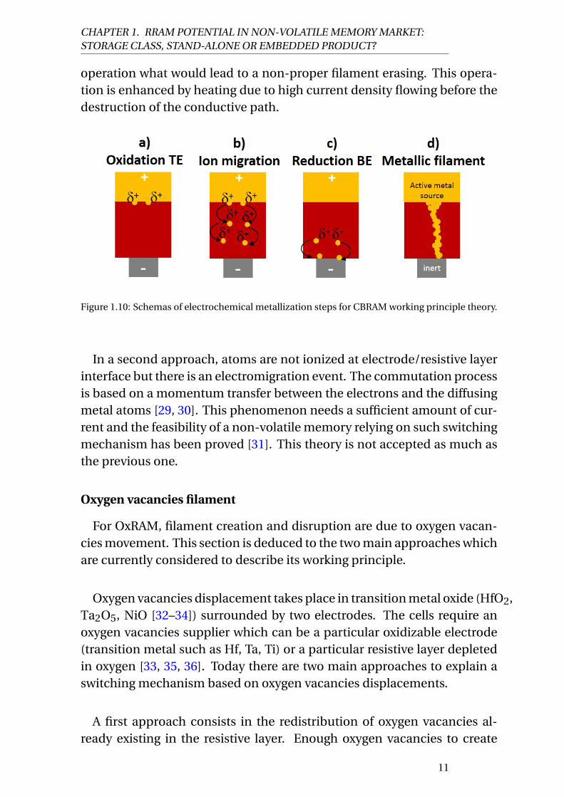
CHAPTER 1. RRAM POTENTIAL IN NON-VOLATILE MEMORY MARKET:STORAGE CLASS, STAND-ALONE OR EMBEDDED PRODUCT?
operation what would lead to a non-proper filament erasing. This opera-tion is enhanced by heating due to high current density flowing before thedestruction of the conductive path.
Figure 1.10: Schemas of electrochemical metallization steps for CBRAM working principle theory.
In a second approach, atoms are not ionized at electrode/resistive layerinterface but there is an electromigration event. The commutation processis based on a momentum transfer between the electrons and the diffusingmetal atoms [29, 30]. This phenomenon needs a sufficient amount of cur-rent and the feasibility of a non-volatile memory relying on such switchingmechanism has been proved [31]. This theory is not accepted as much asthe previous one.
Oxygen vacancies filament
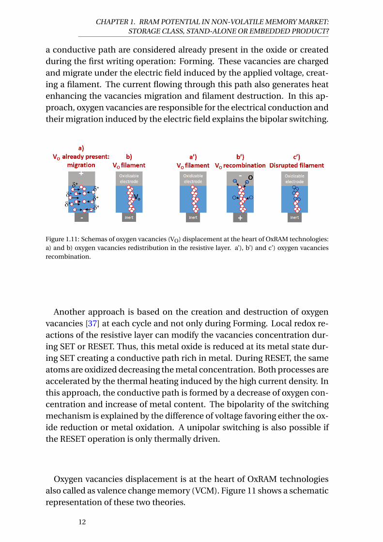
For OxRAM, filament creation and disruption are due to oxygen vacan-cies movement. This section is deduced to the two main approaches whichare currently considered to describe its working principle.
Oxygen vacancies displacement takes place in transition metal oxide (HfO2,Ta2O5, NiO [32–34]) surrounded by two electrodes. The cells require anoxygen vacancies supplier which can be a particular oxidizable electrode(transition metal such as Hf, Ta, Ti) or a particular resistive layer depletedin oxygen [33, 35, 36]. Today there are two main approaches to explain aswitching mechanism based on oxygen vacancies displacements.
A first approach consists in the redistribution of oxygen vacancies al-ready existing in the resistive layer. Enough oxygen vacancies to create
11
CHAPTER 1. RRAM POTENTIAL IN NON-VOLATILE MEMORY MARKET:STORAGE CLASS, STAND-ALONE OR EMBEDDED PRODUCT?
a conductive path are considered already present in the oxide or createdduring the first writing operation: Forming. These vacancies are chargedand migrate under the electric field induced by the applied voltage, creat-ing a filament. The current flowing through this path also generates heatenhancing the vacancies migration and filament destruction. In this ap-proach, oxygen vacancies are responsible for the electrical conduction andtheir migration induced by the electric field explains the bipolar switching.
Figure 1.11: Schemas of oxygen vacancies (VO) displacement at the heart of OxRAM technologies:a) and b) oxygen vacancies redistribution in the resistive layer. a’), b’) and c’) oxygen vacanciesrecombination.
Another approach is based on the creation and destruction of oxygenvacancies [37] at each cycle and not only during Forming. Local redox re-actions of the resistive layer can modify the vacancies concentration dur-ing SET or RESET. Thus, this metal oxide is reduced at its metal state dur-ing SET creating a conductive path rich in metal. During RESET, the sameatoms are oxidized decreasing the metal concentration. Both processes areaccelerated by the thermal heating induced by the high current density. Inthis approach, the conductive path is formed by a decrease of oxygen con-centration and increase of metal content. The bipolarity of the switchingmechanism is explained by the difference of voltage favoring either the ox-ide reduction or metal oxidation. A unipolar switching is also possible ifthe RESET operation is only thermally driven.
Oxygen vacancies displacement is at the heart of OxRAM technologiesalso called as valence change memory (VCM). Figure 11 shows a schematicrepresentation of these two theories.
12

CHAPTER 1. RRAM POTENTIAL IN NON-VOLATILE MEMORY MARKET:STORAGE CLASS, STAND-ALONE OR EMBEDDED PRODUCT?
Resistance change
RRAM working principle is based on cell resistance change dependingon the amount of current flowing. There are several hypotheses to explainoxygen vacancies and metal ions electrical conduction. Depending on re-sistive state (high or low) different mechanism are invoked.
In the case of metal ion conductive path, standard Ohm conduction isgenerally employed [37, 38]. This conduction form is also used to simplifythe HRS electrical conduction but with a strongly reduced conductivity.It is important to note that it exists a continuum [39] of states between afully formed filament in LRS and a fully dissolved in HRS. During the earlystages of RESET, the filament thickness is greatly reduced at a constrictionpoint. Once the constriction is small enough (few atoms), the electricalconduction can be tied to a Quantum Point Contact conduction [40–42].This conduction is attributed to the very low amount of atoms allowing thecurrent to flow, resulting in a quantum conduction in one dimension. Fol-lowing the filament dissolution, shortly after it breaks and a gap appearsbetween both top and bottom side of the filament, in this case the conduc-tion can be explained by Fowler–Nordheim tunneling [43, 44]. With theRESET progression, the gap increases and charge trap might appear in thegap during the process. The last conduction model, bonded to theses trapsrelies on Trap Assisted Tunneling (TAT) [45–47]. It can be noted as well thatsome study has been performed on oxide dealing with filament formationdue to sub-oxides [48].
Dielectric breakdown
OxRAM technology is based on the reversible creation of oxygen vacan-cies in a dielectric such as HfO2, Al2O3... A parallel can be made with oxidebreakdown. For a dielectric, one of its main property is to not conduct thecurrent. When a potential difference is applied to a dielectric, a leakagecurrent is observed. This is due do charge traps already present post pro-cess and allow a small current path. For a good insulator, this current isof the order of 10–12A. Figure 1.12 presents a dielectric current evolutionover time when this one is under a constant bias. This curve can be cut in3 different zones.
In zone 1, the current is decreasing over time representing the absorp-tion of charges that the dielectric can sustain due to its own charge traps.
13

CHAPTER 1. RRAM POTENTIAL IN NON-VOLATILE MEMORY MARKET:STORAGE CLASS, STAND-ALONE OR EMBEDDED PRODUCT?
In zone 2, current is increasing demonstrating a creation of new traps,defects, to allow current flow.
This phenomenon gets out of control zone 3, where an avalanche ofdefect creation happens and leads to breakdown meaning the dielectricbecomes conductor [20]. This breakdown can be controlled if a limitedamount of current is permitted by an exterior device. In this case, some ofthe traps can be annihilated. RRAM forming step can be correlated to thisdescription (see Figure 1.9b). Some device models use this knowledge toput in equation RRAM behavior especially using a percolation model [49].
Figure 1.12: Schema of a dielectric current vs time response under constant bias. Zone 1: chargeabsorption, Zone 2: new traps creation, Zone 3: breakdown.
1.4 Towards RRAM Industrialization: RRAM potential in mem-ory market
1.4.1 History
The first migration of silver ion in a porous material has been publishedin 1954 [50]. Putting a potential difference on a material sandwiched bytwo Ag electrodes, Ag migration is observed. But a memory device is notyet in the idea. In 1964, memory effect is demonstrated in a metal/insulator/metal(MIM) structure, namely Au/SiO/Au [51]. At the time it was hypothesizedthat such a structure could have been used as a memory device whichcould be accessed non-destructively. In the ensuing years similar phe-nomena were found in an Al/SiOx/Au system [52, 53]. Due to stability is-sues and the successful development of Si based memories [54], resistiveswitching memories were put aside until quite recently.
14

CHAPTER 1. RRAM POTENTIAL IN NON-VOLATILE MEMORY MARKET:STORAGE CLASS, STAND-ALONE OR EMBEDDED PRODUCT?
In 2002, W.W. Zhuang et al. demonstrated an RRAM device based onPCMO which could have greater performances than Flash devices [55]. In2004, Samsung Electronics demonstrated resistive switching behavior invarious transition metal oxides (TMO) such as NiO, TiO2, HfO2 and ZrO2with promising characteristics such as an operating voltage below 3V, aprogramming current around 2mA and an endurance of 106 cycles [56].In parallel, memory effect are published using metal ion migration.
For CBRAM, the first researches were mostly devoted to a large screen-ing of the material combinations offering the switching mechanisms bymetal migration in a resistive layer. For this matter, a great interest on theuse of chalcogenide has grown and a lot of researches were presented onvarious resistive layers and electrodes combinations. For example GeTe[57], GST [58], ZnxCd1–xS [59, 60] or Cu2S [61, 62]. GexSy and GexSey werethe two most studied components mainly coupled with silver top electrodebut various bottom electrodes such as Tungsten, Platinium or Nickel [63].This technology was growing in interest but limitations appeared. Tem-perature stability was one of the most important as it can limit CBRAMintegration in CMOS integrated circuits due to the high temperatures usedin standard back-end-of-line processing. More research intend to improveits stability using different chalcogenide stoichiometry or doping [64] buta big change appeared when the resistive layer was replaced by an oxide.
Oxide offers a higher thermal stability and is a well-known material inmicroelectronic which will help process integration. The materials screen-ing researches has thus been conducted on oxides such as Al2O3, Ta2O5,HfO2, mainly coupled with copper top electrode.
1.4.2 RRAM for the actual memory market
To emerge in memory market, one need to think about the place of RRAMand its specifications depending on the target. Several memory architec-tures could be considered depending on technology performances and cost.
RRAM for Stand-alone application
As flash devices start to face key technological issues, alternative mem-ory is envisaged. However, as this technology is cheap and mature, ag-gressive specifications in terms of cost and density are required. RRAMadvancement for stand-alone applications were presented in [16, 65] but
15

CHAPTER 1. RRAM POTENTIAL IN NON-VOLATILE MEMORY MARKET:STORAGE CLASS, STAND-ALONE OR EMBEDDED PRODUCT?
RRAM technologies face difficulties to reach flash maturity. Moreover, al-though 2D flash topological method is expected to reach its practical limitby 2020, 3D flash technology starts to emerged and will lead the semi-conductor industry towards the next revolution in transistor density [14].RRAM technology is not expected anymore for stand-alone applicationunless a major breakthrough occurs.
RRAM for Embedded application
Another idea is to target embedded market. As presented in the begin-ning of the chapter, each application will need specific criteria. RRAMtechnology already prove its potential for this market. For automotive ap-plication, high temperature stability is required and is demonstrated in[15, 66, 67]. For low power application, [28, 68] can be cited.
RRAM for computing systems hierarchy
The last market RRAM could integrate would be in computing systemshierarchy as a storage class memory (like HDD) or as a working memory(like DRAM). In terms of storage, there are two possibilities: placing RRAMbetween hard disk and DRAM or replacing hard disk (see Table 1.3). Toaccess this market, RRAM would need to reach a retention stability over 10years at 85C, a latency below 5µs and an endurance superior to 106 withhigh density product. RRAM advancement for storage class applicationswere presented in [16, 65].
Table 1.3: RRAM specifications for Storage class applications
class memory type latency Endurance Retention Cost Power consumption
storage replacing hard disk < 5µs > 106 10years 85C < 2∗ flash < flash
storage between hard disk and DRAM < 5µs > 106 10years 85C ∼ flash < flash
In a second case, RRAM could replace or support DRAM. It would thenneed a latency lower than 50ns as demonstrated in [28, 69], retention aroundfew days is enough and a great endurance as demonstrated in [33, 70] (seeTable 1.4).
Table 1.4: RRAM specifications for working memory
class memory type latency Endurance Retention Cost Power consumption
working memory replacing DRAM < 50ns > 109 > 5days 85C < 12 DRAM < DRAM
working memory between hard disk and DRAM < 200ns > 109 > 5days 85C < 12 DRAM < DRAM
16

CHAPTER 1. RRAM POTENTIAL IN NON-VOLATILE MEMORY MARKET:STORAGE CLASS, STAND-ALONE OR EMBEDDED PRODUCT?
Nowadays, RRAM show some limitations before being able to integratethis market. Four issues remain challenging: window margin variability,forming operation, programming current and trade-off between enduranceand retention. Today, the main research efforts have been focused on im-proving device performances, dimensions and physical understanding, plac-ing RRAM technology after the peak of its interest (see Figure 1.13). Re-search is now waiting for an industrial to challenge the technology.
expectations
time
On the Rise
At the Peak
Sliding IntoThe Trough
ClimbingThe Slope
EnteringThe Plateau
R&D
Startup companiesfirst round of venture
capital funding
First-generationproducts, high price,lots of customization
needed
Early adoptersinvestigate
Mass mediahype begins
Supplier proliferation
Activity beyondEarly adopters
Negativepress begins
Supplier consolidationand failures
Second/thirdrounds of
venture capitalfunding
Less than 5% of the potential audience
has adopted fully
Second-generationproducts,
some services
Methodologies and best practices developing
Third-generation products, out of the box, product
suites
High-growth adoptionphase starts: 20% to 30%
of the potentialaudience has adopted
the innovation
TechnologyTrigger
Peak of InflatedExpectations
Trough ofDisillusionment
Slope ofEnlightenment
Plateau ofProductivity
RRAM
Figure 1.13: RRAM maturity level [71]
1.4.3 RRAM improvement: work in research for theoretical understand-ing
Microscopic observation
Following CMOS development tracks, RRAM presents a lack of theoret-ical bases. The working principle is not yet fully understood and some re-searches are devoted to physically observe RRAM switching mechanism.However, as conductive paths width is supposed to be in nanometer range,literature does not give entire satisfaction. Research is still devoted to RRAMobservation, dreaming of a device real-time switch movie with in-situ trans-mission electron microscopy (TEM).
17

CHAPTER 1. RRAM POTENTIAL IN NON-VOLATILE MEMORY MARKET:STORAGE CLASS, STAND-ALONE OR EMBEDDED PRODUCT?
For example in 2011, B. Cho showed a bistable switching mechanismbehavior related to the formation and rupture of highly conductive pathsin a Ag/polymerstructure using TEM and energy-dispersive X-ray spec-troscopy [72] following in 2012 by Y. Yang et al who published a direct TEMimaging of metal ion/oxide structures showing a metallic conductive path[73]. These results comforted CBRAM principle with a filament composedof metal ions coming from an active electrode which can be formed anddisrupted with a bipolar behavior.
In parallel, Q.Liu et al observed in real time a growth and dissolutionof conductive filaments in Oxide-Electrolyte-Based RRAM supporting itsworking principle description: there was no silver in the Pristine state whileafter forming, Ag is highly detected. After Reset, there is still some Ag de-tected but in lower concentration showing that the initial state is not recov-ered. There is a multifilamentary observation. Conductive filaments arefound to start growing from the TE rather than having to reach the BE andgrow backwards and have a conical base at the TE interface [74]. This re-sult allows to give a filament shape closer to reality for simulation althoughit is still in debate.
More recently, in 2014, U. Celano et al used conductive atomic force mi-croscopy to observe the conductive zones in a switched device. They ex-trapolated the results in a 3D image showing a conical filament with itsbase at the TE. They showed as well, using scanning probe microscopy(SPM), that the constriction of the CFs is below 10 x 10 nm2 indicating astrong scalability potential for OxRAM devices [75, 76].
Figure 1.14: Observation of conducting filament dynamics in SiO2-based resistive memories [73].
18

CHAPTER 1. RRAM POTENTIAL IN NON-VOLATILE MEMORY MARKET:STORAGE CLASS, STAND-ALONE OR EMBEDDED PRODUCT?
Simulation and Modelling
To support microscopic observation, simulation works are carried out.Among these researches, a lot of effort are put into first principles cal-culations which allow the computation of various properties (electronic,mechanical, energetic. . . ) of a material. However, these calculations arestrongly limited by the number of atoms it can simulate. Only few atomscan be simulated in a relative short time duration (few days to weeks),which makes it impossible to simulate a whole RRAM cell. However, it cangive insights on defects creation and behavior in one of the layer. For ex-ample, defect energy levels and defect energy migration barriers can beextracted. To give an example of the impact of these works, we can focuson Al2O3 as a resistive layer.
To study a possible filament composed of oxygen vacancies, VO diffusionhas been studied for different charge state [77] with a description of defectlevels [78, 79] giving an idea on the energy cost of creating this filament.
On the other hand, K. Sankaran et al studied in an amorphous Al2O3the diffusion barrier of different defects such as Cu and Te showing a verylow Cu diffusion barrier in the case of porous Al2O3 [80] accentuating on aCBRAM behavior study and support a Cu filament.
To go further, J. A. Dawson and J.Robertson use three different filamentmodels in Al2O3, showing that the strong binding between Cu interstitialsdrives filament formation, resulting in Al ions being driven out of the Cu-rich environment [81]. This result gives insight on a copper based filamentformation.
In the same idea, X. Xu et al compared different Cu filament density (3 to7 atoms of Cu) and show that small changes in the filament structure canlead to large changes in the current-voltage characteristic in atomic scalefilaments which can explain a multi-level resistances in RRAM [82].
Staying in electrical characteristics, T.V. Perevalov et al show that elec-tron and hole capture on oxygen vacancy in γ – Al2O3 is an energeticallyfavorable process [83].
19

CHAPTER 1. RRAM POTENTIAL IN NON-VOLATILE MEMORY MARKET:STORAGE CLASS, STAND-ALONE OR EMBEDDED PRODUCT?
Figure 1.15: Activation energies (eV) of VO diffusion on four pathways at different charge states inAl2O3. Al in red, O in white and VO in yellow [77].
These studies can be done on other material such as HfO2 [84–87], Ta2O5[88–90]... to comfort or refute some hypothesis following a microscopicobservation or an electrical behavior. Moreover, using these calculationresults and experimental inputs, device models have been developed fol-lowing various electrical conduction hypothesis such as Ohmic currentthrough highly resistive layer [37, 38, 91], Fowler-Nordheim tunneling [43,44], Trap Assisted Tunneling [45–47] or Quantum-Point-Contact [40–42].
From CBRAM/OxRRAM to Hybrid RAM
Most of the results presented in this manuscript were obtained on oxide-based CBRAM. This technology has been motivated by the complementaryadvantages of chalcogenide CBRAM and OxRRAM. Chalcogenide CBRAMtechnology is well known for having a high ROFF/RON ratio and a low powerconsumption while OxRRAM has a high temperature stability and high cy-cling. By combining both technologies, having an oxide as resistive layerand an active Top Electrode, this new device may allow to obtain all advan-tages in one technology. However, understanding the working principle ofthis oxide-based CBRAM is even more challenging. They may combineoxygen vacancy and metal ion movements if TE/oxide are well chosen. Inthis case, we will talk about Hybrid RRAM (HRRAM) in this manuscript.
20

CHAPTER 1. RRAM POTENTIAL IN NON-VOLATILE MEMORY MARKET:STORAGE CLASS, STAND-ALONE OR EMBEDDED PRODUCT?
Figure 1.16: Motivation to go from CBRAM/OxRRAM to HRRAM.
1.5 Chapter I synthesis
RRAM technologies present great advantages to enter the memory mar-ket thanks to ease of integration in the Back end of Line and high density.They could integrate three different kinds of market: storage class, stand-alone applications and embedded systems. For each target, different spec-ifications are needed. Some of them were demonstrated in literature butRRAM still present some technological issues which place RRAM after itspeak of interest, waiting for an industrial to challenge the technology.
Today, various physical mechanisms can explain CBRAM and OxRRAMswitching behavior. They rely on a conductive path formation and disrup-tion, called filament, in a resistive layer. In the case of CBRAM, filamentis composed of metallic elements coming from the active top electrodewhile in OxRRAM, it is composed of oxygen vacancies created in the ox-ide resistive layer. At the beginning of CBRAM technology, chalcogenidessuch as GeS2 was chosen with mainly Ag as active top electrode. However,due to high temperature stability issues and hoping to improve windowmargin and power consumption compare to OxRRAM technology, oxide-based CBRAM were tested. In this case, filament can be composed of oxy-gen vacancies and top electrode metallic element. Our laboratory baptizedthis technology, combining both type of filament, Hybrid RRAM (HRRAM).This transition to HRRAM brought new challenges to overcome such ashigher voltages and higher forming step than CBRAM and endurance canbe degraded compare to OxRRAM. Optimization of this technology is stillon going and in the same time, as physical understanding is lacking, mi-
21

CHAPTER 1. RRAM POTENTIAL IN NON-VOLATILE MEMORY MARKET:STORAGE CLASS, STAND-ALONE OR EMBEDDED PRODUCT?
croscopic observation and simulations bring more and more knowledgeconcerning switching mechanism and material properties impact for eachstack layer.
In order to optimize HRRAM materials, simulation and electrical char-acterization are carried out in parallel in CEA-Leti. Simulations support orrefute hypothesis brought by experimental results to clarify RRAM work-ing principle and evaluate material properties impact on the stacks. In thismanuscript, both skills has been developed to combine atomistic simula-tion and electrical characterization. Various RRAM performances are eval-uated to target different types of market from storage to embedded. OxR-RAM and HRRAM are characterized considering several oxygen density.Then, material properties are investigated by atomistic simulation givingmicroscopic parameters to link RRAM performances and chosen materi-als.
To introduce this work, next chapter will describe the studied samplesand the characterization methods that has been used to evaluate RRAMperformances. Then, third chapter will explain atomistic simulation the-ory basis and used methods to extract RRAM microscopic properties. Thesetwo chapters will serve as basis to the results presented in the following ofthe manuscript. Then, in the fourth chapter we will present the result onfilament microscopic understanding combining experimental and simula-tion results. Chaper five will fully developed microscopic properties effecton HRRAM performances and present some technological key to choosematerials for a given application. Finally, chapter six will synthesis andgive the perspectives of this work.
22

Bibliography
[1] T. Global. Connected Life, connectedlife.tnsglobal.com, 2016. 2
[2] M. Armbrust, A. Fox, R. Griffith, A. D. Joseph, R. Katz, A. Konwinski,G. Lee, D. Patterson, A. Rabkin, I. Stoica, and M. Zaharia. A Viewof Cloud Computing. Commun. ACM, 53(4):50–58, April 2010. doi:10.1145/1721654.1721672. 2
[3] M. Hilbert. The World’s Technological Capacity to Store, Communi-cate, and Compute Information, 2011. 2
[4] KPCB. Internet Trends Report, http://www.kpcb.com/blog/2016-internet-trends-report, 2016. 2
[5] A. Osys. Flash Storage Trends, https://www.slideshare.net/OsysAG/flash-storage-werner-eggli-osys-tech-talk. ix, 3
[6] Y.-H. Shih. 3d Charge Trapping (CT) NAND Flash,http://www.sematech.org/meetings/archives/symposia/10187/,2011. 2
[7] ITRS. Emerging research devices, 2013. ix, xv, 2, 5, 8
[8] Fujitsu. Fujitsu and Tokyo Institute of Technology Announce the De-velopment of New Material for 256mbit FeRAM Using 65-nanometerTechnology - Fujitsu United States, 2006. 5
[9] T. Instrument. FRAM – New Generation of Non-Volatile Memory,2008. 5
[10] C. Muller. Mémoires ferroélectriques FRAM : principe, limitations,innovations, applications. Hermès science, pages 425–451, 2011. 6
[11] FRAM | Ferroelectric RAM Technology | Theory & Operation. ix, 6
[12] M. Julliere. Tunneling between ferromagnetic films. Physics Letters A,54(3):225–226, September 1975. doi: 10.1016/0375-9601(75)90174-7.6
23
BIBLIOGRAPHY
[13] M. Wuttig and N. Yamada. Phase-change materials for rewriteabledata storage. Nature Materials, 6(11):824–832, November 2007. doi:10.1038/nmat2009. 7
[14] ITRS. Executive Report, 2015. 7, 16
[15] J. R. Jameson, P. Blanchard, C. Cheng, J. Dinh, A. Gallo, V. Gopalakr-ishnan, C. Gopalan, B. Guichet, S. Hsu, D. Kamalanathan, D. Kim,F. Koushan, M. Kwan, K. Law, D. Lewis, Y. Ma, V. McCaffrey, S. Park,S. Puthenthermadam, E. Runnion, J. Sanchez, J. Shields, K. Tsai,A. Tysdal, D. Wang, R. Williams, M. N. Kozicki, J. Wang, V. Gopinath,S. Hollmer, and M. V. Buskirk. Conductive-bridge memory (CBRAM)with excellent high-temperature retention. In 2013 IEEE InternationalElectron Devices Meeting, pages 30.1.1–30.1.4, December 2013. doi:10.1109/IEDM.2013.6724721. 8, 16
[16] S. Sills, S. Yasuda, J. Strand, A. Calderoni, K. Aratani, A. Johnson,and N. Ramaswamy. A copper ReRAM cell for Storage Class Mem-ory applications. In 2014 Symposium on VLSI Technology (VLSI-Technology): Digest of Technical Papers, pages 1–2, June 2014. doi:10.1109/VLSIT.2014.6894368. 8, 15, 16
[17] ISSCC. MEMORY – 2013 Trends. International Solid-State CircuitsConference, February 2013. ix, 8
[18] S. Menzel, U. Böttger, M. Wimmer, and M. Salinga. Physics ofthe Switching Kinetics in Resistive Memories. Advanced Func-tional Materials, 25(40):6306–6325, October 2015. doi: http://onlinelibrary.wiley.com/doi/10.1002/adfm.201500825/abstract. 9
[19] R. Waser, R. Dittmann, G. Staikov, and K. Szot. Redox-Based ResistiveSwitching Memories – Nanoionic Mechanisms, Prospects, and Chal-lenges. Advanced Materials, 21(25-26):2632–2663, July 2009. doi: http://onlinelibrary.wiley.com/doi/10.1002/adma.200900375/abstract. 9,10
[20] M. Saadi, P. Gonon, C. Vallée, C. Mannequin, H. Grampeix,E. Jalaguier, F. Jomni, and A. Bsiesy. On the mechanisms ofcation injection in conducting bridge memories: The case ofHfO2 in contact with noble metal anodes (Au, Cu, Ag). Jour-nal of Applied Physics, 119(11):114501, March 2016. doi: http://scitation.aip.org/content/aip/journal/jap/119/11/10.1063/1.4943776.14
24

BIBLIOGRAPHY
[21] G. Molas, E. Vianello, F. Dahmani, M. Barci, P. Blaise, J. Guy, A. Tof-foli, M. Bernard, A. Roule, F. Pierre, C. Licitra, B. D. Salvo, andL. Perniola. Controlling oxygen vacancies in doped oxide basedCBRAM for improved memory performances. In 2014 IEEE Interna-tional Electron Devices Meeting, pages 6.1.1–6.1.4, December 2014.doi: 10.1109/IEDM.2014.7046993.
[22] C. Nail, G. Molas, P. Blaise, G. Piccolboni, B. Sklenard, C. Cagli,M. Bernard, A. Roule, M. Azzaz, E. Vianello, C. Carabasse, R. Berthier,D. Cooper, C. Pelissier, T. Magis, G. Ghibaudo, C. Vallée, D. Be-deau, O. Mosendz, B. D. Salvo, and L. Perniola. UnderstandingRRAM endurance, retention and window margin trade-off using ex-perimental results and simulations. In 2016 IEEE International Elec-tron Devices Meeting (IEDM), pages 4.5.1–4.5.4, December 2016. doi:10.1109/IEDM.2016.7838346. 9
[23] I. Valov, I. Sapezanskaia, A. Nayak, T. Tsuruoka, T. Bredow,T. Hasegawa, G. Staikov, M. Aono, and R. Waser. Atomically controlledelectrochemical nucleation at superionic solid electrolyte surfaces.Nature Materials, 11(6):530–535, June 2012. doi: 10.1038/nmat3307.10
[24] S. Z. Rahaman, S. Maikap, W. S. Chen, H. Y. Lee, F. T. Chen, T. C. Tien,and M. J. Tsai. Impact of TaOx nanolayer at the GeSex/W interfaceon resistive switching memory performance and investigation of Cunanofilament. Journal of Applied Physics, 111(6):063710, March 2012.doi: 10.1063/1.3696972. 10
[25] S. Maikap, S. Z. Rahaman, T. Y. Wu, F. Chen, M. J. Kao, and M. J.Tsai. Low current (5 pA) resistive switching memory using high-kTa2o5 solid electrolyte. In 2009 Proceedings of the European Solid StateDevice Research Conference, pages 217–220, September 2009. doi:10.1109/ESSDERC.2009.5331517. 10
[26] A. Chen, J. Hutchby, V. Zhirnov, G. Bourianoff, and J. . S. Wiley. Emerg-ing Nanoelectronic Devices, 2015. 10
[27] J. R. Jameson, N. Gilbert, F. Koushan, J. Saenz, J. Wang,S. Hollmer, M. Kozicki, and N. Derhacobian. Quantized Con-ductance in Ag/GeS_2/W Conductive-Bridge Memory Cells.IEEE Electron Device Letters, 33(2):257–259, February 2012. doi:10.1109/LED.2011.2177803. 10
25

BIBLIOGRAPHY
[28] A. Belmonte, W. Kim, B. Chan, N. Heylen, A. Fantini, M. Houssa,M. Jurczak, and L. Goux. 90nm WAl2o3tiwcu 1t1r CBRAM cellshowing low-power, fast and disturb-free operation. In 2013 5thIEEE International Memory Workshop, pages 26–29, May 2013. doi:10.1109/IMW.2013.6582089. 10, 16
[29] H. Suga, T. Sumiya, M. Horikawa, S. Kumaragurubaran, T. Shimizu,and Y. Naitoh. Threshold Current Density of the Resistance Switchingin Pt Nanogap Electrode. Japanese Journal of Applied Physics, 50(6S):06GF11, June 2011. doi: 10.1143/JJAP.50.06GF11. 11
[30] D. O. Bellisario, Z. Ulissi, and M. S. Strano. A Quantitative andPredictive Model of Electromigration-Induced Breakdown of MetalNanowires. The Journal of Physical Chemistry C, 117(23):12373–12378,June 2013. doi: 10.1021/jp4035776. 11
[31] T. Takahashi, S. Furuta, Y. Masuda, S. Kumaragurubaran, T. Sumiya,M. Ono, Y. Hayashi, T. Shimizu, H. Suga, M. Horikawa, and Y. Naitoh.4kb nonvolatile nanogap memory (NGpM) with 1 ns programmingcapability. In 2012 IEEE Silicon Nanoelectronics Workshop (SNW),pages 1–2, June 2012. doi: 10.1109/SNW.2012.6243334. 11
[32] B. Govoreanu, G. S. Kar, Y. Y. Chen, V. Paraschiv, S. Kubicek, A. Fantini,I. P. Radu, L. Goux, S. Clima, R. Degraeve, N. Jossart, O. Richard, T. Van-deweyer, K. Seo, P. Hendrickx, G. Pourtois, H. Bender, L. Altimime, D. J.Wouters, J. A. Kittl, and M. Jurczak. 10x10nm2 Hf/HfOx crossbar resis-tive RAM with excellent performance, reliability and low-energy op-eration. In 2011 International Electron Devices Meeting, pages 31.6.1–31.6.4, December 2011. doi: 10.1109/IEDM.2011.6131652. 11
[33] M.-J. Lee, C. B. Lee, D. Lee, S. R. Lee, M. Chang, J. H. Hur, Y.-B. Kim,C.-J. Kim, D. H. Seo, S. Seo, U.-I. Chung, I.-K. Yoo, and K. Kim. A fast,high-endurance and scalable non-volatile memory device made fromasymmetric Ta2o(5-x)/TaO(2-x) bilayer structures. Nature Materials,10(8):625–630, July 2011. doi: 10.1038/nmat3070. 11, 16
[34] L. Courtade, C. Turquat, C. Muller, J. G. Lisoni, L. Goux, D. J.Wouters, D. Goguenheim, P. Roussel, and L. Ortega. Oxidation ki-netics of Ni metallic films: Formation of NiO-based resistive switch-ing structures. Thin Solid Films, 516(12):4083–4092, April 2008. doi:10.1016/j.tsf.2007.09.050. 11
[35] Z. Fang, X. P. Wang, J. Sohn, B. B. Weng, Z. P. Zhang, Z. X. Chen,Y. Z. Tang, G. Q. Lo, J. Provine, S. S. Wong, H. S. P. Wong, and D. L.
26

BIBLIOGRAPHY
Kwong. The Role of Ti Capping Layer in HfOx-Based RRAM Devices.IEEE Electron Device Letters, 35(9):912–914, September 2014. doi:10.1109/LED.2014.2334311. 11
[36] Y. Y. Chen, L. Goux, S. Clima, B. Govoreanu, R. Degraeve, G. S. Kar,A. Fantini, G. Groeseneken, D. J. Wouters, and M. Jurczak. En-durance/Retention Trade-off on HfO2/Metal Cap 1t1r Bipolar RRAM.IEEE Transactions on Electron Devices, 60(3):1114–1121, March 2013.doi: 10.1109/TED.2013.2241064. 11
[37] M. Bocquet, D. Deleruyelle, H. Aziza, C. Muller, J. M. Portal, T. Cabout,and E. Jalaguier. Robust Compact Model for Bipolar Oxide-Based Re-sistive Switching Memories. IEEE Transactions on Electron Devices, 61(3):674–681, March 2014. doi: 10.1109/TED.2013.2296793. 12, 13, 20
[38] S. Larentis, F. Nardi, S. Balatti, D. C. Gilmer, and D. Ielmini. Resis-tive Switching by Voltage-Driven Ion Migration in Bipolar RRAM-PartII: Modeling. IEEE Transactions on Electron Devices, 59(9):2468–2475,September 2012. doi: 10.1109/TED.2012.2202320. 13, 20
[39] L. Goux, K. Sankaran, G. Kar, N. Jossart, K. Opsomer, R. Degraeve,G. Pourtois, G. M. Rignanese, C. Detavernier, S. Clima, Y. Y. Chen,A. Fantini, B. Govoreanu, D. J. Wouters, M. Jurczak, L. Altimime, andJ. A. Kittl. Field-driven ultrafast sub-ns programming in WAl2o3ticute-based 1t1r CBRAM system. In 2012 Symposium on VLSI Technology(VLSIT), pages 69–70, June 2012. doi: 10.1109/VLSIT.2012.6242465.13
[40] J. Suñé, S. Long, C. Cagli, L. Perniola, X. Lian, X. Cartoixà, R. Rurali,E. Miranda, D. Jiménez, and M. Liu. Electrical evidence of atomic-sizeeffects in the conduction filament of RRAM. In 2012 IEEE 11th Inter-national Conference on Solid-State and Integrated Circuit Technology,pages 1–4, October 2012. doi: 10.1109/ICSICT.2012.6467649. 13, 20
[41] R. Degraeve, A. Fantini, S. Clima, B. Govoreanu, L. Goux, Y. Y. Chen,D. J. Wouters, P. Roussel, G. S. Kar, G. Pourtois, S. Cosemans, J. A.Kittl, G. Groeseneken, M. Jurczak, and L. Altimime. Dynamic hourglass model for SET and RESET in HfO2 RRAM. In 2012 Sympo-sium on VLSI Technology (VLSIT), pages 75–76, June 2012. doi:10.1109/VLSIT.2012.6242468.
[42] S. Long, X. Lian, C. Cagli, X. Cartoixà, R. Rurali, E. Miranda, D. Jiménez,L. Perniola, M. Liu, and J. Suñé. Quantum-size effects in hafnium-
27

BIBLIOGRAPHY
oxide resistive switching. Applied Physics Letters, 102(18):183505, May2013. doi: 10.1063/1.4802265. 13, 20
[43] A. Benoist, S. Blonkowski, S. Jeannot, S. Denorme, J. Damiens,J. Berger, P. Candelier, E. Vianello, H. Grampeix, J. F. Nodin,E. Jalaguier, L. Perniola, and B. Allard. 28nm advanced CMOS resistiveRAM solution as embedded non-volatile memory. In 2014 IEEE In-ternational Reliability Physics Symposium, pages 2E.6.1–2E.6.5, June2014. doi: 10.1109/IRPS.2014.6860604. 13, 20
[44] K. Kamiya, M. Young Yang, S.-G. Park, B. Magyari-Köpe, Y. Nishi,M. Niwa, and K. Shiraishi. ON-OFF switching mechanism of resis-tive–random–access–memories based on the formation and disrup-tion of oxygen vacancy conducting channels. Applied Physics Letters,100(7):073502, February 2012. doi: 10.1063/1.3685222. 13, 20
[45] L. Larcher, A. Padovani, O. Pirrotta, L. Vandelli, and G. Bersuker.Microscopic understanding and modeling of HfO2 RRAM devicephysics. In 2012 International Electron Devices Meeting, pages 20.1.1–20.1.4, December 2012. doi: 10.1109/IEDM.2012.6479077. 13, 20
[46] B. Gao, B. Sun, H. Zhang, L. Liu, X. Liu, R. Han, J. Kang, and B. Yu. Uni-fied Physical Model of Bipolar Oxide-Based Resistive Switching Mem-ory. IEEE Electron Device Letters, 30(12):1326–1328, December 2009.doi: 10.1109/LED.2009.2032308.
[47] X. Guan, S. Yu, and H. S. P. Wong. On the Switching Parameter Vari-ation of Metal-Oxide RRAM Part I: Physical Modeling and SimulationMethodology. IEEE Transactions on Electron Devices, 59(4):1172–1182,April 2012. doi: 10.1109/TED.2012.2184545. 13, 20
[48] K. H. Xue, B. Traore, P. Blaise, L. R. C. Fonseca, E. Vianello, G. Mo-las, B. D. Salvo, G. Ghibaudo, B. Magyari-Kope, and Y. Nishi. A Com-bined Ab Initio and Experimental Study on the Nature of ConductiveFilaments in $rm Pt/rm Hfrm O_2/rm Pt$ Resistive Random AccessMemory. IEEE Transactions on Electron Devices, 61(5):1394–1402, May2014. doi: 10.1109/TED.2014.2312943. 13
[49] J. Sune. New physics-based analytic approach to the thin-oxide break-down statistics. IEEE Electron Device Letters, 22(6):296–298, June 2001.doi: 10.1109/55.924847. 14
[50] G. T. Kohraan and J. M. A. d. Bruyne. The migration of silverthrough and on the surface of insulating materials. In 1954 Con-
28

BIBLIOGRAPHY
ference On Electrical Insulation, pages 55–56, October 1954. doi:10.1109/CEI.1954.7513575. 14
[51] P. H. Nielsen and N. M. Bashara. The reversible voltage-induced ini-tial resistance in the negative resistance sandwich structure. IEEETransactions on Electron Devices, 11(5):243–244, May 1964. doi:10.1109/T-ED.1964.15319. 14
[52] J. G. Simmons and R. R. Verderber. New Conduction and Re-versible Memory Phenomena in Thin Insulating Films. Proceed-ings of the Royal Society of London A: Mathematical, Physicaland Engineering Sciences, 301(1464):77–102, October 1967. doi:10.1098/rspa.1967.0191. 14
[53] C. J. Varker and E. M. Juleff. Electron beam recording in SiO2withdirect read-out using the electron beam induced current at a p-njunction. Proceedings of the IEEE, 55(5):728–729, May 1967. doi:10.1109/PROC.1967.5671. 14
[54] J. Dirk. Oxide Resistive RAM (OxRRAM) for scaled NVM application,2009. 14
[55] W. W. Zhuang, W. Pan, B. D. Ulrich, J. J. Lee, L. Stecker, A. Bur-master, D. R. Evans, S. T. Hsu, M. Tajiri, A. Shimaoka, K. Inoue,T. Naka, N. Awaya, A. Sakiyama, Y. Wang, S. Q. Liu, N. J. Wu, andA. Ignatiev. Novel colossal magnetoresistive thin film nonvolatile re-sistance random access memory (RRAM). In Digest. InternationalElectron Devices Meeting,, pages 193–196, December 2002. doi:10.1109/IEDM.2002.1175811. 15
[56] I. G. Baek, M. S. Lee, S. Seo, M. J. Lee, D. H. Seo, D. S. Suh, J. C. Park,S. O. Park, H. S. Kim, I. K. Yoo, U. I. Chung, and J. T. Moon. Highly scal-able nonvolatile resistive memory using simple binary oxide driven byasymmetric unipolar voltage pulses. In IEDM Technical Digest. IEEEInternational Electron Devices Meeting, 2004., pages 587–590, Decem-ber 2004. doi: 10.1109/IEDM.2004.1419228. 15
[57] C.-J. Kim, S.-G. Yoon, K.-J. Choi, S.-O. Ryu, S.-M. Yoon, N.-Y. Lee, andB.-G. Yu. Characterization of silver-saturated Ge–Te chalcogenide thinfilms for nonvolatile random access memory. Journal of Vacuum Sci-ence & Technology B: Microelectronics and Nanometer Structures Pro-cessing, Measurement, and Phenomena, 24(2):721–724, March 2006.doi: 10.1116/1.2180260. 15
29

BIBLIOGRAPHY
[58] R. Pandian, B. J. Kooi, G. Palasantzas, J. T. M. De Hosson, andA. Pauza. Polarity-dependent reversible resistance switching inGe–Sb–Te phase-change thin films. Applied Physics Letters, 91(15):152103, October 2007. doi: 10.1063/1.2798242. 15
[59] Z. Wang, P. B. Griffin, J. McVittie, S. Wong, P. C. McIntyre, and Y. Nishi.Resistive Switching Mechanism in ZnxCd1-xS Nonvolatile MemoryDevices. IEEE Electron Device Letters, 28(1):14–16, January 2007. doi:10.1109/LED.2006.887640. 15
[60] P. van der Sluis. Non-volatile memory cells based on ZnxCd1-xS fer-roelectric Schottky diodes. Applied Physics Letters, 82(23):4089–4091,June 2003. doi: 10.1063/1.1581365. 15
[61] S. W. Kim and Y. Nishi. Copper sulfide-based resistance change mem-ory. In 2007 Non-Volatile Memory Technology Symposium, pages 76–78, November 2007. doi: 10.1109/NVMT.2007.4389951. 15
[62] T. Sakamoto, N. Banno, N. Iguchi, H. Kawaura, H. Sunamura,S. Fujieda, K. Terabe, T. Hasegawa, and M. Aono. A Ta2o5solid-electrolyte switch with improved reliability. In 2007 IEEESymposium on VLSI Technology, pages 38–39, June 2007. doi:10.1109/VLSIT.2007.4339718. 15
[63] M. N. Kozicki and W. C. West. Programmable metallization cellstructure and method of making same, June 1998. U.S. Classification365/182, 365/100, 365/107, 257/E45.002; International ClassificationH01L27/105, H01L27/04, H01L27/10, H01B1/06, H01L21/822,H01B1/10, G02F1/19, G11C13/00, H01L21/82, G02F1/155,G11C13/02, G02F1/15, H01L45/00, G06F12/00; Cooperative Clas-sification G11C2213/51, H01L45/1233, G11C13/0069, G02F1/1525,H01L45/142, H01L45/1206, G11C2013/009, G02F1/155, H01L45/085,H01L45/1213, G11C13/0011, H01L45/1226; European Classifica-tion G11C13/00R25W, G11C13/00R5B, H01L45/12B, H01L45/08M,H01L45/12D2, H01L45/12C, H01L45/14B2, H01L45/12D4,G02F1/15W2. 15
[64] E. Vianello, G. Molas, F. Longnos, P. Blaise, E. Souchier, C. Cagli,G. Palma, J. Guy, M. Bernard, M. Reyboz, G. Rodriguez, A. Roule,C. Carabasse, V. Delaye, V. Jousseaume, S. Maitrejean, G. Reimbold,B. D. Salvo, F. Dahmani, P. Verrier, D. Bretegnier, and J. Liebault. Sb-doped GeS2 as performance and reliability booster in Conductive
30

BIBLIOGRAPHY
Bridge RAM. In 2012 International Electron Devices Meeting, pages31.5.1–31.5.4, December 2012. doi: 10.1109/IEDM.2012.6479145. 15
[65] L. Zhao, Z. Jiang, H. Y. Chen, J. Sohn, K. Okabe, B. Magyari-Köpe, H. S. P. Wong, and Y. Nishi. Ultrathin (2nm) HfOx as thefundamental resistive switching element: Thickness scaling limit,stack engineering and 3d integration. In 2014 IEEE InternationalElectron Devices Meeting, pages 6.6.1–6.6.4, December 2014. doi:10.1109/IEDM.2014.7046998. 15, 16
[66] R. Strenz. Embedded Flash technologies and their applications: Sta-tus amp; outlook. In 2011 International Electron Devices Meeting,pages 9.4.1–9.4.4, December 2011. doi: 10.1109/IEDM.2011.6131521.16
[67] Z. Wei, K. Eriguchi, S. Muraoka, K. Katayama, R. Yasuhara, K. Kawai,Y. Ikeda, M. Yoshimura, Y. Hayakawa, K. Shimakawa, T. Mikawa, andS. Yoneda. Distribution projecting the reliability for 40 nm ReRAMand beyond based on stochastic differential equation. In 2015 IEEEInternational Electron Devices Meeting (IEDM), pages 7.7.1–7.7.4, De-cember 2015. doi: 10.1109/IEDM.2015.7409650. 16
[68] L. Goux, K. Opsomer, R. Schuitema, R. Degraeve, R. Muller, C. De-tavernier, D. J. Wouters, M. Jurczak, L. Altimime, and J. A. Kittl.Self-Limited Filament Formation and Low-Power Resistive Switch-ing in CuxTe1-x/Al2o3/Si CBRAM Cell. In 2011 3rd IEEE Inter-national Memory Workshop (IMW), pages 1–4, May 2011. doi:10.1109/IMW.2011.5873219. 16
[69] K. Aratani, K. Ohba, T. Mizuguchi, S. Yasuda, T. Shiimoto, T. Tsushima,T. Sone, K. Endo, A. Kouchiyama, S. Sasaki, A. Maesaka, N. Ya-mada, and H. Narisawa. A Novel Resistance Memory with HighScalability and Nanosecond Switching. In 2007 IEEE InternationalElectron Devices Meeting, pages 783–786, December 2007. doi:10.1109/IEDM.2007.4419064. 16
[70] C. W. Hsu, I. T. Wang, C. L. Lo, M. C. Chiang, W. Y. Jang, C. H. Lin,and T. H. Hou. Self-rectifying bipolar TaOx/TiO2 RRAM with superiorendurance over 1012 cycles for 3d high-density storage-class memory.In 2013 Symposium on VLSI Technology, pages T166–T167, June 2013.16
31

BIBLIOGRAPHY
[71] G. Molas. Breaking the memory bottleneck in computingapplications-part II in Design and Technology Eneblers for Comput-ing Applications, 2016. ix, 17
[72] B. Cho, J.-M. Yun, S. Song, Y. Ji, D.-Y. Kim, and T. Lee. Direct Obser-vation of Ag Filamentary Paths in Organic Resistive Memory Devices.Advanced Functional Materials, 21(20):3976–3981, October 2011. doi:10.1002/adfm.201101210. 18
[73] Y. Yang, P. Gao, S. Gaba, T. Chang, X. Pan, and W. Lu. Observation ofconducting filament growth in nanoscale resistive memories. NatureCommunications, 3:732, March 2012. doi: 10.1038/ncomms1737. ix,18
[74] Q. Liu, J. Sun, H. Lv, S. Long, K. Yin, N. Wan, Y. Li, L. Sun, and M. Liu.Real-Time Observation on Dynamic Growth/Dissolution of Conduc-tive Filaments in Oxide-Electrolyte-Based ReRAM. Advanced Materi-als, 24(14):1844–1849, April 2012. doi: 10.1002/adma.201104104. 18
[75] U. Celano, L. Goux, A. Belmonte, K. Opsomer, A. Franquet, A. Schulze,C. Detavernier, O. Richard, H. Bender, M. Jurczak, and W. Vander-vorst. Three-Dimensional Observation of the Conductive Filamentin Nanoscaled Resistive Memory Devices. Nano Letters, 14(5):2401–2406, May 2014. doi: http://dx.doi.org/10.1021/nl500049g. 18
[76] U. Celano, G. Giammaria, L. Goux, A. Belmonte, M. Jurczak, andW. Vandervorst. Nanoscopic structural rearrangements of the Cu-filament in conductive-bridge memories. Nanoscale, 8(29):13915–13923, July 2016. doi: 10.1039/C5NR08735J. 18
[77] M. Y. Yang, K. Kamiya, B. Magyari-Köpe, M. Niwa, Y. Nishi, and K. Shi-raishi. Charge-dependent oxygen vacancy diffusion in Al2o3-basedresistive-random-access-memories. Applied Physics Letters, 103(9):093504, August 2013. doi: 10.1063/1.4819772. ix, 19, 20
[78] J. R. Weber, A. Janotti, and C. G. Van de Walle. Point Defects in Al2o3and Their Impact on Gate Stacks. Microelectron. Eng., 86(7-9):1756–1759, July 2009. doi: 10.1016/j.mee.2009.03.059. 19
[79] D. Liu, S. J. Clark, and J. Robertson. Oxygen vacancy levels and elec-tron transport in Al2o3. Applied Physics Letters, 96(3):032905, January2010. doi: 10.1063/1.3293440. 19
32

BIBLIOGRAPHY
[80] K. Sankaran, L. Goux, S. Clima, M. Mees, J. A. Kittl, M. Jurczak,L. Altimime, G.-M. Rignanese, and G. Pourtois. Modeling of Cop-per Diffusion in Amorphous Aluminum Oxide in CBRAM MemoryStack. ECS Transactions, 45(3):317–330, April 2012. doi: http://ecst.ecsdl.org/content/45/3/317. 19
[81] J. A. Dawson and J. Robertson. Nature of Cu Interstitials in Al2o3 andthe Implications for Filament Formation in Conductive Bridge Ran-dom Access Memory Devices. The Journal of Physical Chemistry C,120(27):14474–14483, July 2016. doi: 10.1021/acs.jpcc.6b02728. 19
[82] X. Xu, J. Liu, and M. P. Anantram. Conduction in alumina with atomicscale copper filaments. Journal of Applied Physics, 116(16):163701,October 2014. doi: 10.1063/1.4898073. 19
[83] T. V. Perevalov, A. V. Shaposhnikov, and V. A. Gritsenko. Elec-tronic Structure of Bulk and Defect $\alpha$- and $\gamma$-Al2o3. Microelectron. Eng., 86(7-9):1915–1917, July 2009. doi:10.1016/j.mee.2009.03.006. 19
[84] L. Jinlong, L. Jing, Z. Hongpeng, Y. Jin, J. Xianwei, L. Qi, L. Xi-aofeng, and D. Yuehua. Optimal migration route of Cu inHfO 2. Journal of Semiconductors, 35(1):013001, 2014. doi:10.1088/1674-4926/35/1/013001. 20
[85] L. Zhao, S. Clima, B. Magyari-Köpe, M. Jurczak, and Y. Nishi. Ab initiomodeling of oxygen-vacancy formation in doped-HfOx RRAM: Effectsof oxide phases, stoichiometry, and dopant concentrations. AppliedPhysics Letters, 107(1):013504, July 2015. doi: 10.1063/1.4926337.
[86] B. Traoré, P. Blaise, E. Vianello, L. Perniola, B. D. Salvo, and Y. Nishi.HfO2-Based RRAM: Electrode Effects, Ti/HfO2 Interface, Charge In-jection, and Oxygen (O) Defects Diffusion Through Experiment andAb Initio Calculations. IEEE Transactions on Electron Devices, 63(1):360–368, January 2016. doi: 10.1109/TED.2015.2503145.
[87] N. Capron, P. Broqvist, and A. Pasquarello. Migration of oxygen va-cancy in HfO2 and across the HfO2/SiO2 interface: A first-principlesinvestigation. Applied Physics Letters, 91(19):192905, November 2007.doi: 10.1063/1.2807282. 20
[88] B. Xiao, T. Gu, T. Tada, and S. Watanabe. Conduction pathsin Cu/amorphous-Ta2o5/Pt atomic switch: First-principles stud-
33

BIBLIOGRAPHY
ies. Journal of Applied Physics, 115(3):034503, January 2014. doi:10.1063/1.4861724. 20
[89] H. Jiang and D. A. Stewart. Enhanced oxygen vacancy diffusionin Ta2o5 resistive memory devices due to infinitely adaptive crystalstructure. Journal of Applied Physics, 119(13):134502, April 2016. doi:10.1063/1.4945579.
[90] H. Jiang and D. A. Stewart. Using Dopants to Tune Oxygen Va-cancy Formation in Transition Metal Oxide Resistive Memory. ACSApplied Materials & Interfaces, 9(19):16296–16304, May 2017. doi:10.1021/acsami.7b00139. 20
[91] J. Guy. Evaluation des performances des mémoires CBRAM (Conduc-tive bridge memory) afin d’optimiser les empilements technologiqueset les solutions d’intégration. Grenoble Alpes, December 2015. 20
34

Chapter 2
Studied devices and electricalcharacterization set up
2.1 Introduction/Objectives
During this PhD, several types of devices were studied changing mate-rial stacks and integration for different maturity level. This chapter focuseson explaining all these differences and describes the electrical set up usedto characterize all these devices. Going from a material study, integrat-ing RRAM with a single Resistor (1R device), through a Transistor-Selectorintegration (1T1R device) evaluating performances of one device, to 1Mbarray integration allowing a statistical study significant due to high devicevariability [1–3], this work highlights a need of physical study as well as aneed of industrial bench mark.
2.2 Studied Devices
2.2.1 Material stacks
In order to compare different material performances, variation of stacks,thickness and material deposition methods were used. In a first step, weperform a material research with a simple 1R integration to evaluate if astructure presents promising memory characteristics. The one showinggood performances are then integrated in a 1T1R structure to evaluate per-formances with a better current control avoiding an early device weariness.Finally, the most promising technologies are then integrated in arrays toevaluate devices in industrial environment. This work is based on pre-vious results leading actual effort to study Oxide-based CBRAM. The ba-sic structure is made of an oxide as a resistive layer such as Al2O3, HfO2,Ta2O5, an active Cu-based Top Electrode (TE) and different inert Bottom
35

CHAPTER 2. STUDIED DEVICES AND ELECTRICAL CHARACTERIZATIONSET UP
Electrode (BE) such as W, TiN, TaN. Figure 2.1 shows an example a set ofvarious technologies studied in this work.
3 to 5nmAl2O3
PVD
CuTex
TiN
5 to 10nm HfO2
ALD
CuTex
W
3 to 5nmAl2O3
ALD
CuTex
W
5 to 10nm Ta2O5
PVD/PEALD
CuTex
W
3 to 5nmAl2O3
PVD
CuTex
TaN
Top Electrode
oxide
Bottom Electrode
Figure 2.1: Stacks variation example studied in this work
2.2.2 Integration
Depending on RRAM maturity, various integration processes were usedin this work depending on mask set leading to various memory devicestructures. Depending on base wafer circuits a single device (1R), a tran-sistor plus a device (1T1R) or an array integration can be obtained.
VIA structure
VIA structure is used to verify first process feasibility of a stack, and thenRRAM operation and compare material response. Due to its minimal num-ber of etching/complex pattern, this integration process is fast. However, itdoes not target industrial architecture requirement. Figure 2.2 representsa VIA structure. Bottom Electrode is deposited in a scaled hole motif whichtypically measures between 300nm and 2µm and is called VIA. This layeris covered with resistive layer and Top Electrode which are not patterned.These characteristics imply a common active layer for all devices and avoidimpact of confinement, etching... on material behavior.
Resistive layer
Top Electrode
Bottom Electrode
Metal Line for Contact
Metal Line for ContactInsulator
Figure 2.2: Schema of a VIA structure
36

CHAPTER 2. STUDIED DEVICES AND ELECTRICAL CHARACTERIZATIONSET UP
Mesa structure
In this case, resistive layer and Top Electrode are patterned followingBottom Electrode scale implying that each device has its own switchinglayer separated from the adjacent ones (see Figure 2.3). Confinement ofthe memory is then limited by etching which can be as low as the lithogra-phy technology allows it to be [4].
Resistive layer
Bottom Electrode
Metal Line for Contact
Metal Line for ContactInsulator
Top Electrode
Figure 2.3: Schema of a MESA structure
1R integration
In order to first check RRAM operation, it is integrated in 1 Resistor in-tegration (1R): only RRAM device. This integration is faster than the nextone and allows RRAM investigation at the material level. However, this in-tegration presents limitation from a performance point of view and have alower maximum write and erase operations before device destruction thana 1T1R integration (see description below). This is caused by a lack of cur-rent control which implies an early device degradation. Figure 2.4 com-pares 1R and 1T1R I(V) curves for SET and RESET operations. Even if an ex-terior generator should limit SET current (100µA here), it is visible that themaximum of current flowing during RESET is around 1mA in 1R whereas itshould be equal to the maximum SET current (see 1T1R curves); meaningthe exterior generator was not able to limit enough the real current flowingthrough the memory during Forming and SET. This phenomenon is stillbeing studied [5] and is called overshoot. It is considered to be caused byan uncontrolled electrical capacitance discharge of the bench test cablesin the RRAM, during a brief period of time.
1T1R integration
In order to compensate this current overshoot and improve RRAM per-formances, a current selector is added. In our work, a transistor is playing
37

CHAPTER 2. STUDIED DEVICES AND ELECTRICAL CHARACTERIZATIONSET UP
(a) 1R
-1 0 110-11
10-9
10-7
10-5
10-3
overshoot
RESET
I[A]
V[V]
Ic
SET
(b) 1T1R
-1 0 110-11
10-9
10-7
10-5
10-3
Ic
I[A]
V[V]
RESET SET
Figure 2.4: Typical SET and RESET I(V) curve of a) 1R and b) 1T1R W/Al2O3/CuTex device
the current control role. This integration is called 1 Transistor - 1 Resis-tor (1T1R) (see Figure 2.5) and is essential to improve RRAM performancesby decreasing overshoot current described above and also enables largematrix integration (see below). Today, other kind of selectors are subjectof research to simplify integration process and increase memory density[6, 7].
BE TESource Line (SL)
VSource
World Line (WL)
VGate
Bit Line (BL)
VDrain
1T 1R
Figure 2.5: Schema of 1 Transistor - 1 Resistor (1T1R) configuration
Arrays integration
Next step in RRAM integration to go towards industrial market is ar-ray/matrix integration. In our work, matrices of 4kb to 1Mb are realized.Each single device is a 1T1R cell where transistor is essential to cancel theleakage current (ILeakage) between the cells that would exist in 1R matrix(see Figure 2.6). Removing this leakage current allows to realize high den-sity matrices where in the other case ILeakage would become too important
38
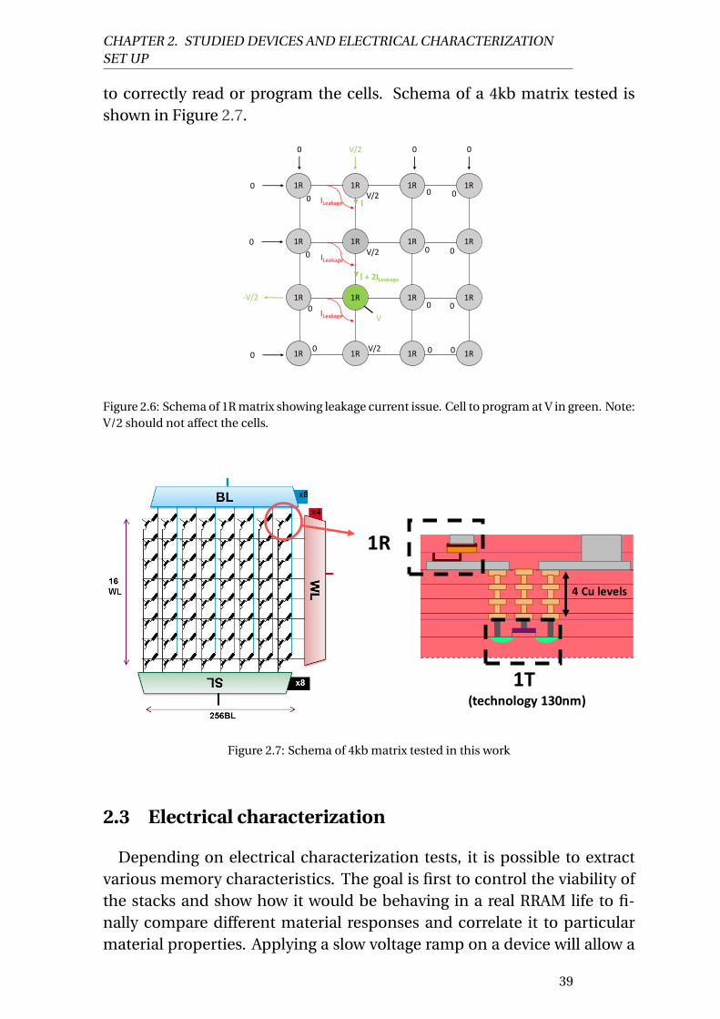
CHAPTER 2. STUDIED DEVICES AND ELECTRICAL CHARACTERIZATIONSET UP
to correctly read or program the cells. Schema of a 4kb matrix tested isshown in Figure 2.7.
1R 1R 1R 1R
1R 1R 1R 1R
1R 1R 1R 1R
1R 1R 1R 1R
V/2
-V/2
0 0 0
0
0
0
ILeakage
ILeakage
ILeakage
I
I + 2ILeakage
V
V/2
V/2
V/2
0
0
0
0
0
0
0
0
0
0
0
0
Figure 2.6: Schema of 1R matrix showing leakage current issue. Cell to program at V in green. Note:V/2 should not affect the cells.
1T (technology 130nm)
1R
4 Cu levels
Figure 2.7: Schema of 4kb matrix tested in this work
2.3 Electrical characterization
Depending on electrical characterization tests, it is possible to extractvarious memory characteristics. The goal is first to control the viability ofthe stacks and show how it would be behaving in a real RRAM life to fi-nally compare different material responses and correlate it to particularmaterial properties. Applying a slow voltage ramp on a device will allow a
39

CHAPTER 2. STUDIED DEVICES AND ELECTRICAL CHARACTERIZATIONSET UP
complete description of a current vs voltage behavior. It is called Quasi-static programming. Switching is then directly visible and voltage switchfor forming, SET and RESET can be extracted. This slow ramp method isnot industrially viable and highly power consuming. Another study, indus-trially real is then necessary to evaluate performances of devices such asnumber of write and erase possible for a given technology, its temperaturestability... It is called pulsed programming.
2.3.1 Quasi-static programming
Quasi-static programming consists in applying a voltage ramp betweendevice Top and Bottom Electrodes and in measuring its current response.During the ramp, the current flowing through the cell is measured with aParameter Analyzer (Agilent 4156 or B1500) and can be internally limitedby a maximum current called compliance current Ic. This compliance isused during forming and SET to avoid a complete degradation of the resis-tive layer which would lead to an irreversible conductive path, destroyingthe device. A typical I(V) curve is shown in Figure 2.8. From these results,characteristic voltages can be extracted such as the voltages where RRAMswitches: they are called VForming, VSET and VRESET for each RRAM event:Forming, SET and RESET respectively. Actual device resistance is acces-sible as well by a READ measurement consisting in a ramp at low voltage(typically from 0 to 0.1V) to keep the actual RRAM state and avoid Readdisturb [8]. Resistance is extracted by a linear regression of this I(V) curveusing Ohm’s law. Quasi-static method is essential to check RRAM function-alities and extract the first features but it is time consuming and far fromindustrial reality. So, another programming test is used to extract shorttime characteristics and industrial like behavior.
2.3.2 pulsed programming
Pulsed programming consists in applying a voltage pulse between TEand BE during a given amount of time. The voltage pulse can be controlledin terms of shape, height, ascending/descending slope and duration. Readoperation can be done as well with a pulse at low voltage (few 100mV),measuring current and doing an Ohm law extrapolation. Read operationis done several times and averaged to have a good accuracy. A compliancecurrent can be applied as well. To accelerate a total time measurement,current calibration is possible. By fixing the range where the expected cur-rent should be, reading operation is faster. This calibration should be well
40

CHAPTER 2. STUDIED DEVICES AND ELECTRICAL CHARACTERIZATIONSET UP
-2 -1 0 1 2 3 4 5 610-14
10-12
10-10
10-8
10-6
10-4
VRESET
VForming
SET
VSET
Forming
I [A
]
Voltage [V]
RESET
tool limit
Figure 2.8: Typical Quasi-static I(V) curves with VForming, VSET and VRESET extraction(W/Al2O3(5nm)/CuTex) [9]
chosen depending on compliance current. If the highest current expectedis around 10–4A, a calibration around 10–6A (which is the maximum cur-rent tolerated) will not read the exact current. The Parameter Analyzer (Ag-ilent 4156 or B1500) has a 3 decades detection amplitude. Therefore, if ONover OFF current ratio is superior to 1000, two different calibrations arenecessary to detect the exact resistances in the two states. For exampleone at 10–4A to detect correctly RON if compliance is around 100µA andone at 10–5A to reach below 10–7A and read ROFF without any error. Oneof the big advantage of pulsing programming is the limited stress seen by acell playing on pulse time duration. This allows to extract the best perfor-mances of a device and is similar to industrial programming.
2.3.3 RRAM characteristics extraction: endurance, retention and win-dow margin
To characterize RRAM, three main performances are extracted: endurance,retention and window margin. Each of this feature can be measured by anelectrical test.
Endurance
Endurance (also called cycling) corresponds to a succession of SET andRESET operations on a single device meaning the cell is written and thenerase as much time as user defines it. After each operation resistance canbe measured to control the efficiency of each operation. From this mea-surement the maximum number of cycles of a technology can be extracted
41

CHAPTER 2. STUDIED DEVICES AND ELECTRICAL CHARACTERIZATIONSET UP
(Ncycle max). It corresponds to the maximum number of Write and Eraseactions possible on a technology before one of the operation fails mean-ing the device can not be written or erased anymore with the chosen con-dition. To perform a high number of cycles (>1000) read operations canbe done punctually on log scale to control if the cell is still working. Thiskind of programming allows to program 107 cycles in one cell in less than2min. However to control the voltage switch variability depending on cy-cling, Quasi-static programming is still required. Figure 2.9 shows a typicalendurance curve up to 108 cycles with 100 successive switching cycles ev-ery decades only (Figure 2.9a with all reading points, Figure 2.9b with astandard deviation on the 100 reads per decade).
(a)
100 102 104 106 108103
104
105
106 Ron
Roff
R [o
hm]
cycles
Ncycles max
(b)
100 102 104 106 108103
104
105
106
R [o
hm]
cycles
Ncycles max
Figure 2.9: Typical endurance curves up to 108 cycles with 100 read every decades a) all readingpoints b) Standard deviation on 100 reading points. Ncycles max represents the maximum numberof cycle the device reached (W/HfO2 (5nm)/CuTex with Ic=1mA and tpulse=1µs)
Retention
Retention measurement (also called temperature stability) consists incontrolling how long a given state (ON or OFF) is going to be stable in dif-ferent temperatures. This feature characterizes the RRAM non-volatilitybehavior meaning how long RRAM keeps the information if it is let un-touched. The cell is first programmed in ON or OFF state by Quasi-staticor pulsed programming and then put in an oven under homogeneous tem-perature (80 to 350 C). Read measurement is performed in a log scale in-terval (usually after 20min, 1h, 4h, 24h, 1 week...) at room temperature. Aslong as there is no resistance variation, the cell is stable, when there is a re-sistance change, it corresponds to the time to failure, tfail, for a given tem-perature (Figure 2.10a). In this manuscript, a minimum resistance vari-
42
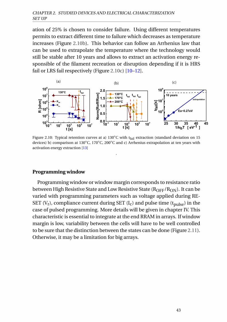
CHAPTER 2. STUDIED DEVICES AND ELECTRICAL CHARACTERIZATIONSET UP
ation of 25% is chosen to consider failure. Using different temperaturespermits to extract different time to failure which decreases as temperatureincreases (Figure 2.10b). This behavior can follow an Arrhenius law thatcan be used to extrapolate the temperature where the technology wouldstill be stable after 10 years and allows to extract an activation energy re-sponsible of the filament recreation or disruption depending if it is HRSfail or LRS fail respectively (Figure 2.10c) [10–12].
(a)
10-1 101 103 105 107103
104
105
106
107
108tfail130°C
R [o
hm]
t [s]
Roff
Ron
(b)
10-1 101 103 105 1070.0
0.5
1.0
1.5
2.0
Norm[R
off/R
on]
t [s]
130°C 170°C 200°C
tfailtfailtfail
(c)
25 30 35 40 45
105
107
109
extrapolation
Ea~0.27eV
t fail[
s]
1/kbT [ eV-1 ]
10 years
Figure 2.10: Typical retention curves at a) 130C with tfail extraction (standard deviation on 15devices) b) comparison at 130C, 170C, 200C and c) Arrhenius extrapolation at ten years withactivation energy extraction [13]
.
Programming window
Programming window or window margin corresponds to resistance ratiobetween High Resistive State and Low Resistive State (ROFF/RON). It can bevaried with programming parameters such as voltage applied during RE-SET (Vr), compliance current during SET (Ic) and pulse time (tpulse) in thecase of pulsed programming. More details will be given in chapter IV. Thischaracteristic is essential to integrate at the end RRAM in arrays. If windowmargin is low, variability between the cells will have to be well controlledto be sure that the distinction between the states can be done (Figure 2.11).Otherwise, it may be a limitation for big arrays.
43

CHAPTER 2. STUDIED DEVICES AND ELECTRICAL CHARACTERIZATIONSET UP
103 104 105 1060.011
10407095
99.5 Ron
Roff
Minimum WM
Nor
mal
Per
cent
iles
R[ohm]
Mean value
Figure 2.11: RON and ROFF distribution associated with Figure 2.9. Mean value and minimumWindow Margin can be extracted
2.4 Chapter II synthesis
This chapter introduced the required notions to apprehend the exper-imental results in the following of the manuscript. The different deviceintegrations were explained and motivated. Standard measurement meth-ods were detailed with RRAM endurance, retention and window marginextraction. In this work, each RRAM technology will be characterized bythese three features. Different RRAM material combinations will be testedand their associated electrical response studied. In parallel, CEA-LETI in-vests in microscopic research to bring some observation on fresh and useddevices. However, as switching mechanism phenomenon has not yet beenobserved and present a lack of comprehension, atomistic simulations havebeen developed. Interactions between RRAM layers can be investigatedand results can give insights on mechanisms that could be at the sourceof a filament formation and disruption. Combining electrical character-ization and atomistic simulation is beneficial to increase RRAM under-standing and can give input for a complete RRAM modelling. This scopewas covered in this work using Density Functional Theory (DFT), allowingto approve or refute some hypothesis resulting from electrical measure-ments. Atomistic simulations theory used in this manuscript is developedin the next chapter.
44

Bibliography
[1] A. Belmonte, R. Degraeve, A. Fantini, W. Kim, M. Houssa, M. Jurczak,and L. Goux. Origin of the current discretization in deep reset statesof an Al2o3/Cu-based conductive-bridging memory, and impact onstate level and variability. Applied Physics Letters, 104(23):233508, June2014. doi: 10.1063/1.4883856. 35
[2] J. Guy, G. Molas, C. Cagli, M. Bernard, A. Roule, C. Carabasse, A. Tof-foli, F. Clermidy, B. De Salvo, and L. Perniola. Guidance to ReliabilityImprovement in CBRAM using Advanced KMC Modelling. IRPS, 2017.
[3] A. Grossi, E. Nowak, C. Zambelli, C. Pellissier, S. Bernasconi,G. Cibrario, K. E. Hajjam, R. Crochemore, J. F. Nodin, P. Olivo, andL. Perniola. Fundamental variability limits of filament-based RRAM.In 2016 IEEE International Electron Devices Meeting (IEDM), pages4.7.1–4.7.4, December 2016. doi: 10.1109/IEDM.2016.7838348. 35
[4] L. Liebmann and J. A. Torres. A Designer’s Guide to Subresolu-tion Lithography: Enabling the Impossible to Get to the 14-nmNode [Tutorial]. IEEE Design Test, 30(3):70–92, June 2013. doi:10.1109/MDAT.2013.2255911. 37
[5] S. Tirano, L. Perniola, J. Buckley, J. Cluzel, V. Jousseaume, C. Muller,D. Deleruyelle, B. De Salvo, and G. Reimbold. Accurate anal-ysis of parasitic current overshoot during forming operation inRRAMs. Microelectronic Engineering, 88(7):1129–1132, July 2011. doi:10.1016/j.mee.2011.03.062. 37
[6] G. W. Burr, R. S. Shenoy, K. Virwani, P. Narayanan, A. Padilla, B. Kurdi,and H. Hwang. Access devices for 3d crosspoint memory. Journalof Vacuum Science & Technology B, Nanotechnology and Microelec-tronics: Materials, Processing, Measurement, and Phenomena, 32(4):040802, July 2014. doi: 10.1116/1.4889999. 38
[7] A. Verdy, G. Navarro, V. Sousa, P. Noe, M. Bernard, F. Fillot, G. Bour-geois, J. Garrione, and L. Perniola. Improved Electrical Performance
45

BIBLIOGRAPHY
Thanks to Sb and N Doping in Se-Rich GeSe-Based OTS Selector De-vices. In 2017 IEEE International Memory Workshop (IMW), pages 1–4,May 2017. doi: 10.1109/IMW.2017.7939088. 38
[8] F. Longnos, E. Vianello, G. Molas, G. Palma, E. Souchier, C. Carabasse,M. Bernard, B. D. Salvo, D. Bretegnier, and J. Liebault. On disturbimmunity and P/E kinetics of Sb-doped GeS2/Ag conductive bridgememories. In 2013 5th IEEE International Memory Workshop, pages96–99, May 2013. doi: 10.1109/IMW.2013.6582107. 40
[9] C. Nail, P. Blaise, G. Molas, M. Bernard, A. Roule, A. Toffoli, L. Perniola,and C. Vallée. Atomistic mechanisms of copper filament formationand composition in Al2o3-based conductive bridge random accessmemory. Journal of Applied Physics, 122(2):024503, July 2017. doi:10.1063/1.4990979. x, 41
[10] G. Muller, T. Happ, M. Kund, G. Y. Lee, N. Nagel, and R. Sezi. Statusand outlook of emerging nonvolatile memory technologies. In IEDMTechnical Digest. IEEE International Electron Devices Meeting, 2004.,pages 567–570, December 2004. doi: 10.1109/IEDM.2004.1419223. 43
[11] R. Symanczyk, R. Bruchhaus, R. Dittrich, and M. Kund. Investi-gation of the Reliability Behavior of Conductive-Bridging MemoryCells. IEEE Electron Device Letters, 30(8):876–878, August 2009. doi:10.1109/LED.2009.2024623.
[12] E. Vianello, G. Molas, F. Longnos, P. Blaise, E. Souchier, C. Cagli,G. Palma, J. Guy, M. Bernard, M. Reyboz, G. Rodriguez, A. Roule,C. Carabasse, V. Delaye, V. Jousseaume, S. Maitrejean, G. Reimbold,B. D. Salvo, F. Dahmani, P. Verrier, D. Bretegnier, and J. Liebault. Sb-doped GeS2 as performance and reliability booster in ConductiveBridge RAM. In 2012 International Electron Devices Meeting, pages31.5.1–31.5.4, December 2012. doi: 10.1109/IEDM.2012.6479145. 43
[13] C. Nail, G. Molas, P. Blaise, G. Piccolboni, B. Sklenard, C. Cagli,M. Bernard, A. Roule, M. Azzaz, E. Vianello, C. Carabasse, R. Berthier,D. Cooper, C. Pelissier, T. Magis, G. Ghibaudo, C. Vallée, D. Be-deau, O. Mosendz, B. D. Salvo, and L. Perniola. UnderstandingRRAM endurance, retention and window margin trade-off using ex-perimental results and simulations. In 2016 IEEE International Elec-tron Devices Meeting (IEDM), pages 4.5.1–4.5.4, December 2016. doi:10.1109/IEDM.2016.7838346. x, 43
46

Chapter 3
Atomistic simulation
3.1 Introduction/Objectives
As microscopic technics are not always efficient to visualize physical events,atomistic simulations are used to extract material properties non-accessibleby experimental methods and to support or refute hypothesis coming fromthese observations. For example, in this work we will be interested in cal-culating the cost of introducing a copper atom in different oxides and seeif it could be energetically favorable to compose a filament. Atomistic cal-culation gives access to known properties as well which help evaluating re-sults veracity. Practically, it consists in calculating a structure composed ofseveral atoms such as a crystal for example and resolve the famous Schrödingerequation to understand how these atoms are linked and how there elec-trons interact with each other.
Based on First Principle calculations (known as ab initio methods), Den-sity Functional Theory (DFT) has proved to be efficient and successful indescribing structural and electronic properties in a vast class of materials,ranging from atom and molecular levels to simple crystals, up to complexextended systems (including glasses and liquids) with a relatively smallcomputational effort. For this reason DFT has become a common inves-tigation tool, which is used in quantum chemistry and physics to find so-lutions to the fundamental equation that describes the quantum behaviorof molecules and condensed matter systems, the Schrödinger equation.Note that the term ab initio does not mean without approximations, butit means without empirical or fitted parameters. This method does notneed any calibration on an experimental base; it directly deals with elec-trons and with approximate quantum calculations. We have performedDFT calculations in order to study filament composition and formation inour different CBRAM. The results give some insights on different filamentcompositions depending on top electrode and oxide. Moreover, it allows to
47

CHAPTER 3. ATOMISTIC SIMULATION
explore thermodynamic and kinetic energies implicated in RRAM workingprinciple for different technologies and extract some material parameterswhich can influence memory characteristics.
3.2 Density functional theory
3.2.1 History
Density Functional Theory is based on the time independent Schrödingerequation resolution which translates the classical mechanic energy con-servation equation in quantum mechanics: total energy of a system is equalto kinetic plus potential energy. It is written as:
HΨ = EΨ (3.1)
WithΨ the wave function related to the probability of finding an electron ina particular region of space, H the Hamiltonian operator which character-izes the kinetic energy plus the potential energy of a given wave functionand E the total energy of the wave function. Any total energy, electronicproperties, thermodynamic properties... of an element with a known elec-tron structure can be calculated with this equation. However, the exact so-lution of this equation is only known for a single hydrogen atom which hasonly one electron. When there are more electrons, Coulomb interactions(interaction between electrons) have to be taken into account. In this case,each electron adds a variable to the wave function Ψ which becomes for Nelectrons at distance ri of its nucleiΨ(r1, r2, ..., rN). As it is not known how tosolve Schrödinger equation with N variables, the first idea was to replacethe wave function by a function which could be defined by one variable. Inthe end of the 20’s Thomas [1] and Fermi [2] proposed then the electronicdensity ρ:
ρ(ri) =∫
...∫Ψ(r1, r2, ..., rn)Ψ(r1, r2, ..., rn)dr1...drn (3.2)
with Ψ the complex conjugate of Ψ. Unfortunately, the way to calculate ex-actly this function was not known and the approximation done presentedsome lack of theory and led to inaccuracies. Therefore, one of the firstmethod to solve Schrödinger equation with N electrons consisted in ap-proximating Ψ(r1, r2, ..., rN) and has been derived in the end of the 30’s byHartree and Fock. Without going into too much details, Hartree consid-ered independent electrons in a central potential due to the core electrons
48

CHAPTER 3. ATOMISTIC SIMULATION
[3] and Fock introduced the Pauli Exclusion Principle allowing to approx-imate the wave functions with a Slater determinant[4]. This system hasbeen refined by Dirac with a Slater determinant sum but it became oner-ous to calculate [5]. In 1964, Honenberg and Kohn established the theoremthat bear their name [6]. It demonstrated that all properties of a system aredetermined by its electronic density ρ. This first part of their theorem filledthe lack of theory of Thomas and Fermi’s idea. In the second part, this the-orem shows that the ground state energy of a wave function, E0, is uniqueand is equal to the one that has the lowest energy:
minE(ρ, ri) = E0 (3.3)
Thus, minimizing a system energy is enough to obtain the ground state en-ergy and density and so describe completely an electronic system groundstate. Following this research, in 1965 Kohn and Sham found a methodto approximate the system electronic density described by Thomas andFermi with good accuracy [7]. Density functional theory is then estab-lished. It can be noted that even today none of exact functional densitiesare known and is still part of DFT approximations.
3.2.2 Solving Schrödinger equation
Kohn and Sham’s approach
Kohn and Sham’s idea is to approximate electronic density by replacing thesystem studied of real particles with an equivalent system composed of in-dependent particles such as these two systems have the same density atground state. The minimum of energy of this new system is equivalent tothe real one and corresponding density can be obtained. Density depend-ing on N wave functions ϕi(r) of free particles can be expressed as:
ρ(r) =N∑
i=1|ϕi(r)|2 (3.4)
To solve Schrödinger equation, the total energy must be equal to HΨ in 3.1.It can be expressed as a sum of energies. Kohn and Sham chose kineticenergy, EKinetic, exchange-correlation energy, EXC, external potential en-ergy, EVext, and Hartree energy, EHartree, and defined them such as the sum
49

CHAPTER 3. ATOMISTIC SIMULATION
depends on the electronic density:
Etotal = EKinetic + EXC + EVext + EHartree
with
EKinetic =1
2
N∑i=1
|~∇ϕi(r)|2
EXC = has been approximated by several methods
EVext =∫
Vext(r)ρ(r)dr
EHartree =1
2
∫ρ(r)ρ(r′)
|r – r′| drdr′
(3.5)
With ϕi the wave functions of free particles, r the distance between elec-trons and its nuclei, Vext the external potential, ρ the electronic density.Exchange-correlation energy, EXC, represents Hartree and Fock’s exchangeenergy and correlation energy between electrons. It has been approxi-mated by several methods leading to a hierarchical level of approxima-tions. This functional choice has to be decided for any calculation and iscommented below.
Functional approximation
To calculate exchange-correlation energy, several types of approximationshave been developed leading to different inacurracy level. We will presentLocal Density Approximation (LDA) developed in the 80’s refined with TheGeneral Gradient Approximation (GGA) in the 90’s. LDA considers elec-trons in a homogeneous gas with N particles with a local density ρ0. Itimplies that the exchange energy of the electrons is calculated as if theywere in an homogeneous gas. The total energy calculated is then underes-timated compare to experimental data. GGA takes into account inhomo-geneous gas of electrons calculating local density variation. Exchange en-ergy depends on ρ(r) and ∇ρ(r) [8]. Calculations are then longer but havea better accuracy with experimental data for bond-lenghts and materialenthalpies. However, for example, Van-der-Waals bond are not well repre-sented and electronic band gap are generally underestimated. To improveGGA approximation, hybrid functionals can be used. However, they arecomputationally costly. Therefore, only punctual comparisions were per-formed to ensure some results.
EXC(LDA) =∫ρ(r)εxc[ρ(r)]dr (3.6)
50

CHAPTER 3. ATOMISTIC SIMULATION
With εxc the local electronic energy [9–11].
Solving the equation
In this section, we present how Kohn-Sham equation is computationallysolved. Presented parameters refer to the code, SIESTA, used in this manuscript.
Schrödinger’s equation solution, giving final system electronic density,is obtained by iterative computation searching to minimize total energy
(δEtotalδϕi(r) = 0). To start calculation, the first density is obtained taking the
sum of atom electronic densities of the system. A first approximation isdone here. To calculate electronic density on an isolated atom, spheri-cal symmetry is considered to be able to solve Kohn-sham equation whichwill depend only on a distance r (one variable). This solution is not ex-act but is close enough from the real one to start calculation and achieveself-consistency. After one iteration, results give a new electronic densitywhich can be reinjected in the loop. Self-consistency is reached when den-sity obtained is close to the one calculated at previous step (convergencecriterion DM.Tolerance in SIESTA). However, this criterion is not enough todetermine if system total energy has been minimized. Indeed if we take forexample cos(x)= x, if x is reinjected, we obtain the same result which doesnot mean that cos(x) has been minimized; it is oscillating. Forces on atomsare then calculated and give new atom positions for the next iteration. Sys-tem is called "minimized" when these calculated forces are smaller than aconvergence criterion (MD.MaxForceTol in SIESTA).
3.2.3 Practical implementation
Forces calculation
In order to optimize atom positions in crystals, applied forces are calcu-lated thanks to adiabatic or Born-Oppenheimer approximation and Hellmann-Feynman theorem [12, 13]. It allows to express forces in terms of atom po-sitions, electronic density and electrostatic energy between atom nuclei.Born-Oppenheimer approximation consists in considering that electronsperceive nuclei as motionless. It can be justified by the fact that due tomass difference between nuclei and electrons, electronic motion is usuallymuch faster than nuclear motion. This lemma allows to decompose theproblem into two parts:
• the solution of the electronic equations under the potential due to thenuclei, which are assumed in fixed positions;
51

CHAPTER 3. ATOMISTIC SIMULATION
Figure 3.1: solving Kohn-Sham equation combined with Force minimization algorithm.
• the solution of the equations for the nuclei considered as classicalparticles prone to the potential generated by the electrons.
Pseudopotentials
In order to reduce time calculation, the full wave function on each atomis not calculated. Instead, only valence electrons are considered becausecore electrons do not participate to material bonding and do not affect ma-terial properties. For example, Silicon has 14 electrons and only 4 electronsare participating to bonding. Therefore, a method has been created to nottake into account all core electrons, called pseudopotentials. These pseu-dopotentials, one for each species, reproduce the potential seen by valenceelectrons. In our calculation Trouiller Martins pseudopotential were used[14].
k-point sampling
Wave functions can be described in different spaces like in real space. How-ever, one of the most efficient way to describe crystal density is the recip-rocal space. In this case, the Brillouin zone (BZ) of a crystal (unit cell in re-ciprocal space) can be divided in a regular grid with k points (kprs = up~b1 +
52

CHAPTER 3. ATOMISTIC SIMULATION
ur~b2+us~b3 with ~bn reciprocal lattice basic vectors) proposed by Monkhorstand Pack [15]. Some of these k points are equivalent, called high symme-try points, allowing to reduce the number of points per grid to calculate.If we solve Schrödinger equation for a periodic system, like a crystal, weneed Bloch’s theorem demonstrating that it is possible to solve Schrödingerequation for each value of k independently. In this case, solution can beexpressed as a sum of terms with the form:
ϕk(r + R) = eik.Rfk(r) (3.7)
with k inside the Brillouin zone vector, and fk(r) a periodic function inspace with the same periodicity as the cell such as fk(r+n1a1+n2a2+n3a3) =fk(r). The more k points are used, the more precise is the result. How-ever, there is a trade-off between the accuracy and the computational cost.Since in our case we are interested in studying point defects, we will needrelatively large cells with a large number of atoms. This implies a small size
of the Brillouin zone (VBZ = (2π)3
Vcell). As a consequence, one obtain a good BZ
sampling with a reduced number of k points.
basis functions
To define fk, DFT calculations use either spatially extended functions (likeplane waves), as in the ABINIT code, or spatially localized functions (likeatomic orbitals), as in the SIESTA code used in this manuscript. The bigadvantage of SIESTA code is time calculation. As it is based on LinearCombination of Atomic Orbitals (LCAO) [16] it reduces matrix size to calcu-late. However, the three parameters defining basis functions need to be ad-justed for each system studied: basis size (orbitals number, SZ, DZ, SZP, DZP),basis extension (orbitals radius, Energy Shift), Grid size (Meshcutoff). Thedisadvantage of this method is the lack of an absolute convergence crite-rion (there is no unique way to enlarge the basis set). In order to verify theaccuracy of basis adopted for SIESTA calculations, it is good to compareresults such as total energy and atomic positions with another method asABINIT, at least for new materials.
3.2.4 Structures and defect calculations
Crystalline structures
To run a simulation, a material model needs to be chosen. To study solidstate, crystalline structures are usually assumed. Crystallography researchesprovide a rich amount of resources with precise crystal description that
53

CHAPTER 3. ATOMISTIC SIMULATION
can be used for simulation initial conditions. For example, in this work,our Al2O3 is deposited as resistive layer and crystallizes in γ-phase. E.Menéndez-Proupin and G. Gutiérrez developed a structure of bulkγ–Al2O3[17]that can be used to start simulations. This spinel-defective structure iscomposed of 40 atoms with 16 Aluminum atoms and 24 Oxygen atoms.This structure, is derived from a spinel MgAl2O4 with two missing atomscreating vacancies (see Figure 3.2).
The first step in DFT is to optimized atom positions in the unit cell ofa crystal based on this model. If the given structure does not give a con-verged result, this model is not stable and does not exist; another one hasto be found. For specific study such as punctual defect, bigger cell needsto be used to avoid too close defect interaction which is not well taken intoaccount in DFT. A structure with several unit cells is then called supercell(see Al2O3 supercell Figure 3.3a).
Figure 3.2: Schema of Al2O3 spinel defective structure. Al in orange, O in pink, vacancies in white.
Amorphous Structures
In our RRAM stack, layers are all amorphous materials. Ideally, an amor-phous model would be chosen. However, characterization and modellingof the atomic and electronic structure of amorphous materials is a com-plicated task due to the random nature of the network. To generate sucha model, one uses a method starting from a crystalline structure, called"melt and quench". Usually a supercell of crystalline material is relaxed bymolecular dynamics: the structure is raised in temperature up to its melt-ing point for a certain amount of time before cooling to room temperature.
54

CHAPTER 3. ATOMISTIC SIMULATION
Figure 3.3: Al2O3 supercell used for calculations. O in red, Al in dark green a) cristaline structurewith a densiy of 3.45g.cm–1 b) amorphous structure with a density of 3.1g.cm–1.
Note that a structure with a lower density (close to experimental) can beartificially built by introducing defects such as vacancies or Schottky de-fect. If the structure does not crystallize again, a disordered structure isobtained (see amorphous Al2O3 calculated structure Figure 3.3b). Beforeusing this amorphous model, one needs to check if electronic propertiesare still correct: material Band Gap needs to be without any defect level.This method is relatively long to relax and sometimes does not give satisfy-ing results at the first shot (defect in the band gap...). Moreover, simulationof defects are much harder than in crystallized structure due to the uniqueposition of each atom, more configuration needs to be treated. That’s whyamorphous model are usually not used for a complete study of a mate-rial but to compare simple calculation with crystalline model to confirmor modulate its results.
Defects in crystal structures
Material’s electronic properties are often controlled by the electrically ac-tive defects and impurities, which usually are a small portion of the totalnumber of defects (?%). In RRAM switching mechanism, defect introduc-tion in dielectric layer could help to form a conductive path. In this respectstate of the art, DFT is a useful method to elucidate the properties of pointdefects and impurities in crystalline structures with relatively low defectconcentrations. This study can then be interpreted to validate or refute hy-pothesis coming from RRAM electrical results or microscopic observation
55

CHAPTER 3. ATOMISTIC SIMULATION
from an atomic point of view. This calculation is used in this work to findthe most favorable defect that could form a filament. This thermodynamicmethod is detailed in the following of the chapter.
Diffusion of Defects
After studying defect properties in dielectrics, the most favorable defectintroductions can be determined. To go further, their movement in theoxide can be studied. Diffusion of defects in solid state can be investigatedin DFT with a popular algorithm called "Nudged Elastic Band" (NEB). Thisstudy gives access to the energy diffusion barrier needed to move an atomfrom one site to another and to a favorable path (3.3.2). In this work, thiscalculation is used to determine which atoms can move in a given oxide toform and disrupt a filament. More details are given in the next section.
3.3 Method
3.3.1 Thermodynamic of the defects
Knowing the cost for introducing a defect in resistive layer is of great inter-est to learn the RRAM switching microscopic mechanism. First, we studythe thermodynamic of the defects in order to determine the most favorableintroduction calculating defect formation energy. Resistive layer existingdefects due to fabrication steps need to be established. In this case, theideal way to study a defect formation energy would be to simulate the fab-rication process. But, it is impossible to simulate a process flow. To over-come this problem, a zero temperature and zero pressure DFT simulationis performed and is combined with thermodynamic chemical potentialstheory. The idea is to use the total energy of a system, obtained by DFTto calculate the Gibbs free energy, ∆G. The Gibbs free energy is the costat which one atom of a given species is exchanged between the oxide andthe surrounding. In our case, Gibbs free energy is reduced to formationenthalpy of the defect,∆H. Temperature and enthropy effects are then ne-glected which is relevant in a solid state at room temperature (∼0.1eV).
Each species need a total energy reference, defined by chemical poten-tials, µ. Some charges, q, can be exchanged as well and need to be takeninto account. Result follows this equation:
∆H = UDefect – UPristine +∑
ni ·µi + q · (EFermi +∆V + EVB) (3.8)
56

CHAPTER 3. ATOMISTIC SIMULATION
Figure 3.4: Illustration of initial and final states calculated to extract defect formation energy∆H. D+q the defect introduced in the oxide, D the complementary defect introduced in TE, qthe charges exchanged.
With ∆H the formation enthalpy of the defect, UDefect the defect to-tal energy, UPristine the initial state total energy, ni and µi the number ofchemical formula and the reference chemical potential for the exchange,q the charges exchanged in the system, EFermi the electrode Fermi levelconsidered in contact, ∆V the electrostatic energy shift[18] and EVB thehighest valence band energy level.
We defined three different cases:
• oxide post process, deposited on a metallic bottom electrode (BE).Oxide is in contact with surrounding gas and BE.
• oxide after top electrode deposition (TE) is then in contact with BEand TE.
• oxide during RRAM switch in contact with TE and BE but can be ini-tially defective.
In the two last cases, the Gibbs free energy will be calculated as the ex-change between the dielectric and the TE. The defect created in oxide willthen generate a complementary defect in TE. For example, if an oxygen isextracted from the oxide, it creates then an oxygen vacancy (VO) in it plusan oxygen interstitial (Oi) in TE. In the TE post process case, as we con-sider exchanges between oxide and TE, formula for a defect charged +q,D+q, generating a complementary defect D in TE becomes:
∆H = Uoxide:D+q – Uoxide + UTE:D – UTE + q · (EFermi +∆V + EVB) (3.9)
With D, the defect introduced in oxide (for example: Cu+1i ), D the com-
plementary defect introduced in TE (for example: VCu) and EFermi the elec-trode Fermi level in contact.
57

CHAPTER 3. ATOMISTIC SIMULATION
Finally, for RRAM working principle case, we study the thermodynamicin defective oxide. Reference for dielectric becomes for example a VO-richoxide (oxide with one VO defect). VO in oxide can come from oxide processcondition in O-poor atmosphere or O exchange with TE. Results are basedon the following equation:
∆H = Uoxide:D
+q00 +D+q – U
oxide:D+q00
+ UTE:D – UTE + (q – q0) · (EFermi +∆V + EVB)
(3.10)
With D+q00 , the defect initially present in defective oxide due to process
or RRAM life, D the studied defect and D its complementary defect in TE.Results give a slope depending on electrode Fermi level EFermi. To ex-
tract the value with the TE considered in contact, this equation can be rep-resented in the range of the oxide bandgap (see Figure 3.5a). Usually, onlythe lowest values are represented which gives the dashed line. Fermi levelthat need to be considered is then deduced with a band alignment betweenoxide and TE (see Figure 3.5b).
(a) Formation enthalpy calculation ofdefects in an oxide depending on Fermilevel.
0 1 2 3 4 5 6-4-202468
1012
slope for each charged defect the most favorable state
D+2
D+1
TE in contact
H
[eV]
Electrode Fermi level relative to oxide BandGap [eV]
D0
(b) schema of a band alignment be-tween an oxide and a metal.
Figure 3.5: Example of defect, D, formation energy results with a metal as TE. TE Fermi level isrepresented and placed on a) with a band alignment shown in b). In a), D+1 is the most favorablestate if the oxide is in contact with the chosen TE.
3.3.2 Diffusion of defects
Transition State Theory (TST)
In order to study diffusion of defects, DFT calculation tools are based onthe transition state theory (TST). TST is used to describe how a chemicalreaction occurs, and is based on the following assumption: between two
58

CHAPTER 3. ATOMISTIC SIMULATION
stable states, called reactant and product, it exists an intermediate state,known as the transition state which is higher in energy. The theory as-sumes that each intermediate is long-lived enough to reach a Boltzmanndistribution of energies before continuing to the next step. When the in-termediates are very short-lived, TST can not be applied: transition statesneed to be in quasi-equilibium with the reactants and products.
TST was developed with the concept of a potential energy surface. Theprogress of a chemical reaction is described as a point in a potential en-ergy surface with coordinates in atomic momenta and distances. The pointpasses through a col or saddle point and reaction rate is determined bythe motion of the system through that col. One of the most importanthypothesis is that transition states are in quasi-equilibrium with the reac-tants. It can be noted that the theory assumes the reaction system will passover the lowest energy saddle point on the potential energy surface. Whilethis description is consistent for reactions occurring at relatively low tem-peratures, at high temperatures, atoms populate higher energy vibrationalmodes; their motion becomes more complex and collisions may lead totransition states far away from the lowest energy saddle point. In this case,another alternatives to transition state theory have to be chosen. TST pos-tulates three major factors that determine whether or not a transition willoccur:
• The concentration of the activated transition state.
• The rate at which the transition state breaks apart.
• The mechanism by which the transition state breaks apart; it can ei-ther be converted into a new stable state, or it can "revert" back to theinitial state.
The reaction rate depends on the probability of finding the system atthe transition state relative to the entire reactant state and on the rate ofcrossing from one state to another at the transition state. To realize thiscalculation, a definition of the transition state needs to be given and in or-der to calculate the probability of being at the transition state, the full par-tition function of the transition state region and the reactant region needto be evaluated. This is computationally challenging and costly when us-ing density functional theory. Therefore, to simplify this calculation, twoassumptions are added:
• The saddle points on the potential energy surface represent “bottleneck” regions that separate reactant from product configurations.
59

CHAPTER 3. ATOMISTIC SIMULATION
• The potential energy surfaces around the reactant configuration andthe saddle point are locally harmonic (quadratic).
The first assumption solves the issue of determining the transition stateby defining it as the hyperplane normal to the unstable direction at thesaddle point. The second assumption allows to have a second order Taylorseries expansion of the potential energy surface at those points leading toa finite number expression to determine the resulting configuration inte-grals needed in TST. These two approximations are relevant for many solid-state reactions. Indeed, the energy barriers are often higher compared tothe average kinetic energy in the system (kBT) ensuring that the systemreaches a local equilibrium between reactive events. To the contrary, if thebarriers are relatively small compared to kBT, the history of the trajectoryis an important factor in determining the reaction rate. This would requirethe use of a more sophisticated statistical model. In another hand, the har-monic approximation is often valid in solid-state reactions. Near the sad-dle points, the potential energy rises rapidly and creates a small bottleneckregion. As counter-example, to describe protein reactions, the potentialenergy can be relatively flat in the region around the saddle point and isnot well characterized by harmonic expansion of the saddle point.
Assuming these assumptions, the first step is to find the saddle point as-sociated with the reaction in question. There are different techniques thatcan be used. In this manuscript, we use Nudged Elastic Band calculations(NEB).
DFT calculation: NEB
The goal is to extract the energy cost of moving a defect in a structure andextract the defect acrivation energy to go from one site to another. In DFT,diffusion of the defects can be studied by a method called Nudged ElasticBand (NEB) calculations. It is a method for finding the minimum energypath (MEP) between two defined points and the potential energy maxi-mum along this MEP is the saddle point energy which gives the activationenergy barrier (see Figure 3.6a)[19]. The method works by optimizing anumber of intermediate images along the reaction path. Each image findsthe lowest energy possible while maintaining equal spacing to neighbor-ing images. This constrained optimization is done by adding spring forcesalong the band between images and by projecting out the component ofthe force due to the potential perpendicular to the band (see Figure 3.6b).Example of results can be seen Figure 3.7.
60

CHAPTER 3. ATOMISTIC SIMULATION
(a) Schema of a potential atom diffu-sion in an energy surface between twochosen states.
(b) Schema of NEB solution generatingseveral images on the most favorablepath.
Figure 3.6: NEB illustrations.
Figure 3.7: Example of migration barrier with associated path screen shots for a defect D1 going toD2.
In order to optimize NEB calculation, one developement consists inconverging one of the images to a saddle point (as opposed to all the im-ages being evenly spaced along the reaction coordinate). This is calledclimbing image NEB and include that the highest energy image is at a sad-dle point [20]. To this aim, this particular image does not feel the springforces along the band and the force along the tangent is inverted. Conse-quently, this image tries to maximize it’s energy along the band, and mini-mize in all other directions. When this image converges, it will be at the ex-act saddle point. It can be noted that in this case, the spacing between im-ages on either side of this image will be different. Some minimization withregular NEB method need to be performed before to define the highest en-ergy image and have a good estimate of the reaction co-ordinate aroundthe saddle point. All NEB calculations presented in this manuscript, areperformed with this method.
61

CHAPTER 3. ATOMISTIC SIMULATION
3.4 Chapter III synthesis
In this chapter, atomistic simulations based on Density Functional Theory(DFT) are presented. History of DFT is exposed and the final calculationtheory and algorithm is explained. It relies on first principle calculationswhich deal directly with electrons and solve Schrödinger equation. It doesnot need any fitting parameters but some approximations are made to cal-culate a system with several electrons. To start this calculation, a structureneeds to be chosen such as a crystal phase. Material properties can then beextracted such as electronic, thermodynamic properties. The second partof the chapter explains how results can be interpreted. As RRAM switchingmechanism is not yet fully explained, these calculations can bring someinsights on filament formation and disruption. In our work, two types ofstudy are presented. First, thermodynamic study is performed in oxide todetermine the most favorable point defects that could lead to a conductivepath formation. DFT calculation gives structure total energy for initial andfinal state; for example without and with defect. Defect formation energycan then be extracted. Afterward, diffusion of defects is investigated to de-termine which species can move in the oxide. This is done by Nudge ElasticBand (NEB) method which is based on transition state theory (TST). It al-lows to calculate a Minimum Energy Path between two defined points andextract its migration energy barrier. At the end of this chapter, exampleof graphic results can be found. Simulation results presented in the nextchapter will be based on these methods and same type of graphics will bepresented.
62

Bibliography
[1] L. H. Thomas. The calculation of atomic fields. Mathematical Pro-ceedings of the Cambridge Philosophical Society, 23(5):542–548, Jan-uary 1927. doi: 10.1017/S0305004100011683. 48
[2] E. Fermi. Un metodo statistico per la determinazione di alcune prior-ietà dell’atome. Rend. Accad. Naz. Lincei, 6:602–607, 1927. 48
[3] D. Hartree. The Wave Mechanics of an Atom with a Non-CoulombCentral Field. Part I. Theory and Methods. Mathematical Proceedingsof the Cambridge Philosophical Society, 24(01):89–110, January 1928.doi: 10.1017/s0305004100011919. 49
[4] V. Fock. Näherungsmethode zur Lösung des quantenmechanischenMehrkörperproblems. Zeitschrift fur Physik, 61:126–148, January1930. doi: 10.1007/BF01340294. 49
[5] P. A. M. Dirac. Note on Exchange Phenomena in the Thomas Atom.Mathematical Proceedings of the Cambridge Philosophical Society, 26(3):376–385, July 1930. doi: 10.1017/S0305004100016108. 49
[6] P. Hohenberg and W. Kohn. Inhomogeneous Electron Gas.Physical Review, 136(3B):B864–B871, November 1964. doi:10.1103/PhysRev.136.B864. 49
[7] W. Kohn and L. J. Sham. Self-Consistent Equations Including Ex-change and Correlation Effects. Physical Review, 140(4A):A1133–A1138, November 1965. doi: 10.1103/PhysRev.140.A1133. 49
[8] J. P. Perdew, K. Burke, and M. Ernzerhof. Generalized Gradient Ap-proximation Made Simple. Physical Review Letters, 77(18):3865–3868,October 1996. doi: 10.1103/PhysRevLett.77.3865. 50
[9] J. P. Perdew and A. Zunger. Self-interaction correction to density-functional approximations for many-electron systems. Physical Re-view B, 23(10):5048–5079, May 1981. doi: 10.1103/PhysRevB.23.5048.51
63

BIBLIOGRAPHY
[10] J. P. Perdew and Y. Wang. Accurate and simple analytic representa-tion of the electron-gas correlation energy. Physical Review B, 45(23):13244–13249, June 1992. doi: 10.1103/PhysRevB.45.13244.
[11] D. M. Ceperley and B. J. Alder. Ground State of the Electron Gas bya Stochastic Method. Physical Review Letters, 45(7):566–569, August1980. doi: 10.1103/PhysRevLett.45.566. 51
[12] H. Hellmann. Einführung in die Quantenchemie. Franz Deuticke,1937. 51
[13] R. P. Feynman. Forces in Molecules. Physical Review, 56(4):340–343,August 1939. doi: 10.1103/PhysRev.56.340. 51
[14] N. Troullier and J. L. Martins. Efficient pseudopotentials for plane-wave calculations. Physical Review B, 43(3):1993–2006, January 1991.doi: 10.1103/PhysRevB.43.1993. 52
[15] H. J. Monkhorst and J. D. Pack. Special points for Brillouin-zoneintegrations. Physical Review B, 13(12):5188–5192, June 1976. doi:10.1103/PhysRevB.13.5188. 53
[16] J. M. Soler, E. Artacho, J. D. Gale, A. García, J. Junquera, P. Ordejón,and Daniel Sánchez-Portal. The SIESTA method for ab initio order-N materials simulation. Journal of Physics: Condensed Matter, 14(11):2745, 2002. doi: 10.1088/0953-8984/14/11/302. 53
[17] E. Menéndez-Proupin and G. Gutiérrez. Electronic properties ofbulk γ – Al2O3. Physical Review B, 72(3):035116, July 2005. doi:10.1103/PhysRevB.72.035116. 54
[18] C. Freysoldt, B. Grabowski, T. Hickel, J. Neugebauer, G. Kresse, A. Jan-otti, and C. G. Van de Walle. First-principles calculations for point de-fects in solids. Reviews of Modern Physics, 86(1):253–305, March 2014.doi: http://link.aps.org/doi/10.1103/RevModPhys.86.253. 57
[19] H. Jónsson, G. Mills, and K. W. Jacobsen. Nudged elastic band methodfor finding minimum energy paths of transitions. pages 385–404, June1998. doi: 10.1142/9789812839664$\_$0016. 60
[20] G. Henkelman, B. P. Uberuaga, and H. Jónsson. A climbing imagenudged elastic band method for finding saddle points and minimumenergy paths. The Journal of Chemical Physics, 113(22):9901–9904,November 2000. doi: 10.1063/1.1329672. 61
64

Chapter 4
RRAM filament composition byatomistic study
4.1 Introduction/Objectives
This chapter is the first of the two chapters combining electrical char-acterization and atomistic simulation to understand the global behaviorof RRAM. References will be made to chapters II and III regarding the de-scription of the characterization protocols and atomistic simulations.
This chapter is dedicated to Al2O3/CuTexGey CBRAM mechanisms atthe microscopic level. As RRAM working principle depends on stack mate-rials and needs to be observed at nanometer resolution, switching mecha-nism understanding is still challenging. We performed electrical tests withsamples having different TE, BE and Al2O3 thickness. Devices are inte-grated in 1-Resistor (1R) and 1-Transistor 1-Resistor (1T1R) configurationsto investigate different electrical answers during forming depending onbottom electrode and polarization voltage. Obtaining different electricalanswer changing TE polarization, atomistic simulations are used to pro-pose, at microscopic level, filament formation differences.
We realize a thermodynamic study for possible ion exchanges betweenAl2O3 and CuTe-based layers to isolate species that could form a filament.We assume two cases: stoichiometric and defective γ-Al2O3 as a model forresistive layer. For the most favorable exchanges, we study defect diffu-sion and extract activation energy employing Nudge Elastic Band methodin DFT. Finally, we combine experiment and simulation to highlight theimpact of oxygen and aluminum point defects in Cu ion insertion and dif-fusion while Te ion comes out unfavorable. A Cu/VO based hybrid filament
65

CHAPTER 4. RRAM FILAMENT COMPOSITION BY ATOMISTIC STUDY
model is proposed and Aluminum Vacancies (VAl) impact on forming pro-cess is discussed.
4.2 Basic review on RRAM working principle
RRAM technologies are based on formation and disruption of a conduc-tive filament (CF) in an electrolyte sandwiched between a top electrode(TE) and a bottom electrode (BE) [1]. Depending on the nature of top elec-trode, filament can be made of oxygen vacancies (OXRRAM) or metal ions(CBRAM). Despite research devoted to CF understanding in RRAM, micro-scopic mechanisms are not conclusive. Most approaches in modelling areconsidering only one chemical element [2, 3] whereas filament composi-tion is probably more complex. One hypothesis supports that oxygen va-cancies (VO) assist copper in the switching mechanism [4–7].
This manuscript focuses its study on oxide-based CBRAM. Its workingprinciple relies on a Cu-rich conductive filament formation inside an in-sulating layer during forming and SET operations [8]. This phenomenon,partially reversible (during RESET operation), allows switching between aLow Resistive State with ON resistance (RON) and a high Resistive Statewith OFF resistance (ROFF) as illustrated in Figure 4.1a. Filament forma-tion in Oxide-based Conductive Bridge RAM involves a Cu-rich conductivefilament inside an oxide based insulating layer [9]. These mechanisms arenot well understood, so we explore the impact of each chemical elementcomposing Al2O3/Cu-based CBRAM.
4.3 Experimental observations
4.3.1 Studied samples
Our measurements are done on different RRAM samples with a BE /Al2O3 / CuTexGey structure (see Figure 4.1a). Large area cells (µm2) areintegrated in 1R or 1T1R configurations. 3.5 to 5nm of amorphous a-Al2O3is deposited by ALD at 300C or by PVD on different PVD bottom electrode(TiN, Ta and W). 20nm of Cu or CuTexGey, deposited by PVD, is used astop electrode (TE).
66

CHAPTER 4. RRAM FILAMENT COMPOSITION BY ATOMISTIC STUDY
(a) Schematic working principle of theAl2O3/CuTexGey-RRAM studied in thiswork. Copper filament (orange) is visu-alized inside dielectric layer
BE
ROn state: current flows
TE:CuTexGey
BE
ROff state: High Resistive state
TE:CuTexGey
ResistiveLayer:Al2O3
20nm
3.5-5nm
SET = V>0 the filament is formed
RESET = V<0 the filament is disrupted
e-
e-
(b) I(V) curve comparing direct (F)and reverse (F) forming depend-ing on TE polarization (VTE) inW/Al2O3(5nm)/CuTexGey sample
-2 -1 0 1 2 3 4 5 6 710-14
10-12
10-10
10-8
10-6
10-4
TE
Al2O3
BE O
TE
Al2O3
BECu
O
|Vf |Vf
SET
VTE<0
VSET
VTE>0
I [A
]
Voltage [V]
RESET
tool limit
Figure 4.1: Schematic working principle and I(V) curve Al2O3/CuTexGey-RRAM
4.3.2 Polarization effect
One of the subject in oxide-based CBRAM is to investigate if there ismetal coming from TE and oxygen vacancies forming the conductive path,as this technology is a result of OxRRAM and CBRAM combination. In or-der to detect if species forming Al2O3/CuTexGey filament are sensible tothe electric field, electrical characterization are performed using differentpolarization.
Figure 4.1b shows typical current-voltage (I-V) characteristics for Al2O3-based CBRAM. To investigate the impact of polarization, two types of form-ing are studied: direct forming, F, and reverse forming F. Direct formingis done at VTE > 0 and reverse forming at VTE < 0. Forming voltage, Vf,can be extracted from this quasi-static measurement (see chapter II) andcan be correlated to alumina breakdown electric field (EBD). EBD measure-ment of 8-9MV/cm shows good agreement with data reported in literature[10], indicating that forming is related to partial oxide breakdown. In otherhand, SET voltage, measured at 1V, is significantly reduced with respect toforming voltage. Moreover, typical OFF state resistance (ROFF) of 1.5x10⁶Ω(obtained after RESET) is measured while initial resistance (measured be-fore forming) is superior to 1013Ω, indicating that initial structure is notrecovered. Thus, SET process requires less energy and may imply differentmechanisms. It can be noted that Vf is slightly smaller when TE is posi-tively polarized (VTE >0). In the following, Vf will refer to the forming volt-age when TE is negatively biased (VTE < 0).
67
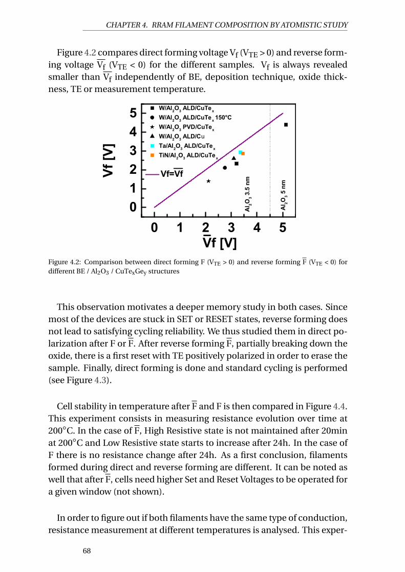
CHAPTER 4. RRAM FILAMENT COMPOSITION BY ATOMISTIC STUDY
Figure 4.2 compares direct forming voltage Vf (VTE > 0) and reverse form-ing voltage Vf (VTE < 0) for the different samples. Vf is always revealedsmaller than Vf independently of BE, deposition technique, oxide thick-ness, TE or measurement temperature.
0 1 2 3 4 5012345
Vf [V
]
Vf [V]A
l 2O3 3
.5 n
m
W/Al2O3 ALD/CuTex
W/Al2O3 ALD/CuTex 150°CW/Al2O3 PVD/CuTex
W/Al2O3 ALD/CuTa/Al2O3 ALD/CuTex
TiN/Al2O3 ALD/CuTex
Vf=Vf
Al 2O
3 5 n
m
Figure 4.2: Comparison between direct forming F (VTE > 0) and reverse forming F (VTE < 0) fordifferent BE / Al2O3 / CuTexGey structures
This observation motivates a deeper memory study in both cases. Sincemost of the devices are stuck in SET or RESET states, reverse forming doesnot lead to satisfying cycling reliability. We thus studied them in direct po-larization after F or F. After reverse forming F, partially breaking down theoxide, there is a first reset with TE positively polarized in order to erase thesample. Finally, direct forming is done and standard cycling is performed(see Figure 4.3).
Cell stability in temperature after F and F is then compared in Figure 4.4.This experiment consists in measuring resistance evolution over time at200C. In the case of F, High Resistive state is not maintained after 20minat 200C and Low Resistive state starts to increase after 24h. In the case ofF there is no resistance change after 24h. As a first conclusion, filamentsformed during direct and reverse forming are different. It can be noted aswell that after F, cells need higher Set and Reset Voltages to be operated fora given window (not shown).
In order to figure out if both filaments have the same type of conduction,resistance measurement at different temperatures is analysed. This exper-
68

CHAPTER 4. RRAM FILAMENT COMPOSITION BY ATOMISTIC STUDY
-4 -3 -2 -1 0 1 2 3 4
V[V]
d)reset
e)set
-4 -3 -2 -1 0 1 2 3 410
-12
10-10
10-8
10-6
10-4
I[A
]
V[V]
a)F
b)1st reset
c)F
Figure 4.3: I(V) curve and interpretation of a W/Al2O3(3.5nm ALD)/CuTexGey cell being formedby a) reverse forming and then b) 1st reset and c) formed again positively before d) and e) standardcycling
100 101 102 103103
104
105
106
107
R [o
hm]
t [s]
Roff F Ron F
Figure 4.4: Retention comparison between direct F and reverse F forming at 200C withISET=100µA for W/Al2O3 ALD 3.5nm/CuTexGey
iment consists in measuring the resistance from 25 to 80C. Initial stateneeds to be reached back to 25C to be sure that resistance evolution isnot due to a filament change. Figure 4.5a shows Resistance vs temperatureevolution (R vs T). Activation energy, Ea can be extracted from this charac-teristics assuming an Arrhenius dependence R ∝ R0exp( Ea
kT). If Ea is high,electronic transport is activated in temperature, supporting a trap assistedconduction as it can be seen for Roff (Figure 4.5b) whereas for Ron a nonactivated electronic transport supports a metalic conduction. There is nodifferences between F and F confirming a filamentary type in both cases.
69

CHAPTER 4. RRAM FILAMENT COMPOSITION BY ATOMISTIC STUDY
(a)
32 33 34 35 36 37 38 39
104
105
Ea=3.28meV
Ea=25.47meV
R [o
hm]
1/KbT (eV-1)
Ron
Roff
(b)
102 104 106 108 101010121014
0
50
100
150Roff
F F
E a [m
eV]
R [ohm]
Ron
Figure 4.5: a) Resistance measurement from 25C to 80C to extract b) Energy of electronic trans-port for different resistances after F and F (W/Al2O3 ALD 3.5nm/CuTexGey).
4.4 Simulations
These experimental results show a difference between filament forma-tion and stability depending on TE polarization. First principle calcula-tions are then used to get more information at microscopic level. In thefirst part, thermodynamic of defects are studied in three cases: existingdefects after Al2O3 deposition, after TE deposition and during RRAM op-eration. In a second part, defect diffusions are investigated.
4.4.1 Simulation framework
For alumina, a 160-atoms supercell consisting of four γ-Al2O3 unit cellsis calculated (see Table 4.1) [11]. This structure is the closest crystallineform of our amorphous ALD material with a density of 3.45 g.cm–3 vs themeasurement value of 3.1 g.cm–3. Different positions are tested for eachdefect, especially for interstitials, up to 4 inequivalent sites are compared(see Figure 4.6). Detailed calculation parameters can be found in Annexe.
The band gap obtained at 3.43eV is corrected in G0W0 at 6.5 eV whichcorresponds to the one measured by ellipsometry [12]. As expected, thisresult of 3.43eV is lower than 7-8eV reported in literature due to GGA ap-proximations, well known for underestimating dielectric bandgap. Correc-tions can be done to extract exact values and estimate error on other results[13]. For TE, we used a 96-atom supercell consisting of eight Cu2Te3Geunit cells [14]. This structure is the closest crystalline form of our amor-phous PVD material with a density of 6.0 g.cm–3 vs 6.1 g.cm–3 (measured).
70

CHAPTER 4. RRAM FILAMENT COMPOSITION BY ATOMISTIC STUDY
Cui1
Cui2
Figure 4.6: γ – Al2O3 and a – Al2O3 structure with different copper interstitial positions circled inorange. O in purple, Al in green black, Cu in orange. Cui1 and Cui2 are mentioned and used formigration barrier calculation
All results are based on a band alignment between band-gap of aluminaand Cu2Te3Ge which is done considering
• G0W0 gap correction with an opening of more than 2eV at conductionband and -0.5 eV at valence band
• Internal Photo-Emission measurement of the barrier of Al2O3/Cu2Te3Geat 3.6eV [15, 16].
To complete the study, an amorphous a-Al2O3 model with a density of3.1 g.cm–3 is implemented (see Table 4.1). This model is generated usingthe melt and quench method (see chapter III): the crystalline triclinic γ-Al2O3 is used for the initial structure at a lower density with the four γ-Al2O3 unit cells considered above. It is melted at 2800K during 10ps andcooled to 300K for 10ps with 1fs time step. 1 k-point is used during molec-ular dynamics while 2*2*2 k-points are used for defect calculations. Bandgap is obtained free of defect at 3.3eV against 3.4eV in crystalline structure.
Table 4.1: Calculated lattice parameters and angles for crytalline γ–Al2O3 and amorphous a–Al2O3
structures
a(A) b(A) c(A) α(deg) β(deg) γ(deg) V(A3/cell) ρ(g/cm3)
γ-Al2O3 11.51 11.43 13.81 89.26 90.00 120.20 392.35 3.45
a-Al2O3 11.30 11.06 13.84 90.20 87.85 119.69 375.29 3.1
71

CHAPTER 4. RRAM FILAMENT COMPOSITION BY ATOMISTIC STUDY
4.4.2 Thermodynamic results
Al2O3 post process defects
In this section, we first study Al2O′3 s native point defects that may ap-
pear after deposition. Calculations are based on the following equation(more details in chapter III):
∆H = UDefect – UPristine +∑
ni ·µi + q · (EFermi +∆V + EVB) (4.1)
With ∆H the formation enthalpy of the defect, UDefect the defect to-tal energy, UPristine the initial state total energy, ni and µi the number ofchemical formula and the reference chemical potential for the exchange,q the charges exchanged in the system, EFermi the electrode Fermi levelconsidered in contact, ∆V the electrostatic energy shift [13] and EVB thehighest valence band energy level.
Results are reported in Figure 4.7. It shows the formation enthalpy ofintrinsic Al2O3 defects depending on oxygen concentration during depo-
sition process (from µO =µO2
2 to metal-rich condition) and considering abottom electrode with a work function close to W. It points out that de-posited Al2O3 may be rich in aluminum Frenkel pair (AlFP) and aluminumvacancies (VAl) charged -3 for O rich condition.
-438 -437 -436 -435
-3
0
3
6VAl
Al2O3
VO+2
Oi0 OFP
VO0
AlFP
Oi-2
VAl-3
Ali+3
O rich
H
[eV]
µO[eV] O poor
Figure 4.7: Formation enthalpy calculation of intrinsic Al2O3 defects. W Fermi level is considered.Yellow zone highlights stoichiometric Al2O3 process conditions.
To summarize these results: deposited Al2O3 may be rich in aluminumFrenkel pair (AlFP) and aluminum vacancies (VAl) charged -3 for O richcondition.
72

CHAPTER 4. RRAM FILAMENT COMPOSITION BY ATOMISTIC STUDY
Al2O3 defects after CuTexGey deposition
Then, we studied aluminum point defects after CuTexGey deposition. Aswe consider exchanges between Al2O3 and CuTe2Ge3, formula for a defectcharged +q, D+q, generating a complementary defect D in TE becomes:
∆H = UAl2O3:D+q – UAl2O3 + UCuTe2Ge3:D – UCuTe2Ge3 + q · (EFermi +∆V + EVB)
(4.2)
With D, the defect introduced in Al2O3 (for example: Cu+1i , Te–2
i ,V0O,V–3
Al ),
D the complementary defect introduced in TE (for example: VCu, VTe, Oi,Ali respectively) and EFermi the electrode Fermi level in contact (for exam-ple W, Cu, Pt or Ti).
Results are presented in Figure 4.8 and the lowest defects are charged.After CuTexGey deposition, considering charge of species and a Fermi levelclose to Cu, the most favorable interstitials and vacancies we could ob-tain are respectively: Copper interstitial (Cu+1
i ), Aluminum vacancy (V–3Al ),
Germanium interstitial (Ge+2i ), Oxygen Vacancy (VO). Tellurium interstitial
(Te–2i ) appears as unfavorable. It can be noted that Ge is used to stabilize
CuTe layer and to keep it amorphous during integration process, to pre-vent any segregation and phase separation. Typically, 10-20% Ge is used[17, 18] in CuTe alloys. As a consequence, Ge is not expected to have anyimpact in the electrical behaviour of CuTe. Moreover, CuTe bound is polarand can easily be broken in Cuδ+ and Teγ– ions. They will be mobile underthe electric field. Ge calculations are just used to confirm this affirmation.We will thus focus on Cu and Te elements in the last section.
To summarize these results: the most favorable defects that can ap-pear in Al2O3 after CuTexGey deposition are: Copper interstitial (Cu+1
i ),Aluminum vacancy (V–3
Al ) and Oxygen Vacancy (VO). Tellurium intersti-
tial (Te–2i ) appears as unfavorable. Germanium interstitial (Ge+2
i ) is lessfavorable than Cui and is just used to stabilize CuTe layer.
Al2O3 defects during RRAM operation
Finally, for CBRAM working principle, we study the case of copper indefective alumina. Reference for oxide becomes either a VO-rich Al2O3
73

CHAPTER 4. RRAM FILAMENT COMPOSITION BY ATOMISTIC STUDY
0 1 2 3 4 5 6-6-4-202468
1012
Gei-4
Gei-2
Gei+2
Tei+2
Tei+1
Tei-2
VAl-3
VO-2
VO-1
VO0
VO+2
Cui+2
Cui+1
W-Cu
H
[eV]
Electrode Fermi level relative to Al 2O3 BandGap [eV]
Cui0
Pt Ti-Al
Figure 4.8: Formation enthalpy calculation of defects in Al2O3/CuTexGey system. Fermi level of 3types of metal (Pt, W-Cu, Ti-Al) are represented (dashed vertical lines).
(Al2O3 with one VO defect) or a AlFP-rich Al2O3 (Al2O3 with one AlFP de-fect) or a V–3
Al -rich Al2O3 (Al2O3 with one V–3Al defect) instead of stoichio-
metric Al2O3. VO in Al2O3 can come from
• Al2O3 process condition in O-poor atmosphere
• O exchange with TE during forming process requiring 5.3eV (Figure 4.8)
AlFP and V–3Al come almost spontaneously from process (Figure 4.7). As
TE is positively polarized during forming, Al+3i insertion in TE is not al-
lowed. Therefore, V–3Al creation does not seem favorable during forming
process. Results are based on the following equation:
∆H = UAl2O3:D
+q00 +D+q – U
Al2O3:D+q00
+ UCuTe2Ge3:D – UCuTe2Ge3
+(q – q0) · (EFermi +∆V + EVB)(4.3)
With D+q00 , the defect initially present in defective Al2O3 due to process
or forming (for example: AlFP, VO or V–3Al ), D the studied defect (Cui, Tei...)
and D its complementary defect in TE (VCu, VTe...).
The most favorable exchanges are highlighted in Table 4.2. Only defectsthat can lead to a conductive path through alumina are taken into account.Defects are then considered when they introduce energy level in aluminaband gap. Cu introduction is favorable in interstitial site or replacing an Alsite. If Al2O3 is VO rich, O substitution is the most favorable. In the case ofAlFP-rich and V–3
Al – rich, Al substitution is the most favorable. We can notethat there is no favorable state found for a Tellurium insertion and that Geinsertion is very expensive compare to Cu.
74

CHAPTER 4. RRAM FILAMENT COMPOSITION BY ATOMISTIC STUDY
Table 4.2: Exchange energy ∆H (eV) between TE and γ-Al2O3. Al2O3 is either stoichiometric or in-cludes oxygen vacancies or aluminum Frenkel pairs or aluminum vacancies
Defect D ∆H Al2O3 (eV) ∆H AlFP-rich (eV) ∆H VO-rich (eV) ∆H V–3Al -rich (eV)
Cu+1i 2.5 2 31 x
(CuAl + Ali)+1 1.1 2 0.6 3 3.2 x
Cu–2Al 5.6 x x 3.2
Cu+1O 5.8 8 0.6 4 x
VO 5.3 x x x
V–3Al 2.8 x x x
AlFP 0.7 x x x
Te–2i 10 8.5 7 x
Te–3Al 7.4 x x 7.3
Ge+2O 9.6 x 3.3 x
1 Cu interstitial defect next to VO already present in Al2O3 with VO2 AlFP is created and Cu substitute Al site3 Cu substitute Al site already present in Al2O3 with AlFP4 Cu substitute O site already present in Al2O3 with VO
To summarize these results: the most favorable defect in a VO-richAl2O3 structure is Cu by O substitution. In the case of AlFP-rich and V–3
Al –rich, Cu by Al substitution is the most favorable. Tellurium and Germa-nium insertions are very expensive compare to Cu.
4.4.3 Amorphous comparison
To complete these results, same calculations are performed in amorphous-Al2O3 (see structure in Figure 4.6). Up to 4 positions are tested for eachdefect. Table 4.3 reports the most favorable ones. Trends are similar toγ – Al2O3: Cui is the most favorable defect that can be inserted in stoi-chiometric Al2O3 and a VO-rich structure decreases Cu energy insertion.However, it can be noted that tested positions for CuAl + Ali are more ex-pensive than Cui. This may be improved by searching new positions. Itcan be noted that it may be due to crystalline structure specificity. The restof the calculations will be done with crystalline structure only, to optimizecalculation time. Results on CuAl + Ali will need to be cautious.
To summarize these results: the most favorable defect in a-Al2O3 is Cuiand Cu by O substitution in a VO-rich structure. These amorphous re-sults are similar to crystalline structure. However, CuAl + Ali need to becautiously treated; it appears more expensive than Cui in the amorphous
75

CHAPTER 4. RRAM FILAMENT COMPOSITION BY ATOMISTIC STUDY
Table 4.3: Formation energies (∆H) in stoichiometric or VO-rich a-Al2O3 calculated in GGA con-sidering exchanges with a Cu2Te3Ge Top Electrode
Defect ∆H Al2O3 (eV) ∆H VO-rich-Al2O3 (eV)
Cu+1i 2.1 2.4
CuAl+Al+1i 2.6
Cu+1O 6 1.65
Cu–2Al 5
VO 3-fold 5.1
V–3Al 3.1
Ge+2i 3.2
Te–2i 4.0
structure.
4.4.4 Diffusion in Al2O3
Cu and Te diffusions
While thermodynamic approach only considers initial and final defectenergy states, more insights are required to quantify the energetic barrierto diffuse Cu ion in Al2O3. For this purpose, energy migration barriers arecalculated using NEB-based (Nudged Elastic Band) approaches. Resultscorrespond to migrations from Cui1 site to Cui2 (see Figure 4.6). It can benoted that in this work, defect formation energy barrier are not considered.This would require an interface model between Al2O3 and CuTexGey withcharge injection effect [19] which is well beyond the scope of this study.However we are in the case of non reversible dielectric breakdown duringforming with a high local electric field. This particular event is happen-ing at non equilibrium. Therefore, we expect the first limiting event to bethe sensibility of species to the electric field. With high diffusion barrier,it is indeed impossible to move in resistive layer. In the case of Ag/GeS2CBRAM behavior with very low migration barrier and low local electricfield this defect formation energy barrier could be the first limiting eventand would need to be calculated.
Cu+i diffusion barrier in Al2O3 structure is found close to 4eV (Figure 4.9a).
Cu migration barriers in defective alumina structures are calculated as wellwith a VO or AlFP next to Cu migration path. In particular, Cu+
i diffusionbarriers in Al2O3-VO and in Al2O3-AlFP are evaluated at 1.4eV and 0.7eV
76

CHAPTER 4. RRAM FILAMENT COMPOSITION BY ATOMISTIC STUDY
respectively. Cu can pass through CuO or CuAl – Ali state. Consequently,oxygen vacancies and aluminum vacancies in Al2O3 would be very likelyto facilitate Cu diffusion. It can be noted that Te–2
i migration in AlFP-rich
Al2O3 is evaluated at more than 7eV (not shown) while Te–3Al migration in
V–3Al -rich is evaluated at 3.1eV (Figure 4.9b).
(a)
0 5 10 15 20 25
0
2
4
Cui2
Cui1
Cui1 Cui2
Cui2
Cui1
dh
Ea
E[eV
]
d[Å]
Cui+1 +AlFP +VO
(b)
-2 0 2 4 6 8 10 12 14 16
0
1
2
3
Tei2Tei1
E[eV
]d[Å]
Figure 4.9: First principle calculations to compute barrier height to diffuse from Cui1 to Cui2 sites(see Figure 4.6) a) Cu+1
i in stoichiometric or defective Al2O3 systems and b) Tei in V–3Al -rich Al2O3
To summarize these results: Te diffusion in V–3Al is evaluated at 3.1eV
while Cu+1i diffusion is the most favorable next to VO or AlFP with a mi-
gration barrier of 1.4eV and 0.7eV respectively.
O and Al diffusions
In order to find out if oxygen or aluminum can be favorable in Al2O3 tohelp Cu diffusion, O2–
i , VO, Al3+i and V3–
Al migration barriers are evaluated.Results are shown in Figure 4.10 with associated path screen shots. It re-veals that oxygen interstitial and aluminum vacancy have the lowest bar-riers. Indeed, we find oxygen vacancy diffusion barrier at 3.4eV and 4.7eVfor threefold and fourfold coordinated oxygen respectively. This really highvalue indicates that VO is immobile. Aluminum interstitial charged +3 isquite hard to diffuse directly from one site to another (>5.5eV not shown).A more favorable path is found by concerted movement and barrier is eval-uated around 2.3eV. Meanwhile, oxygen interstitial and aluminum vacancyhave their highest barrier around 0.54eV and 1.5eV respectively (by con-certed movement).
77

CHAPTER 4. RRAM FILAMENT COMPOSITION BY ATOMISTIC STUDY
(a)
0 2 4 6
0
2
4
E[eV]
d[Å]
VO
Oi
-2VO1
VO2
VO1
VO2
Oi1
Oi2
Oi1
Oi2
(b)
-2 0 2 4 6 8 10 12 14 16
0
1
2
E[eV]
d[Å]
Ali
+3
VAl
-3Al
1
2Ali1
1 1 221
Al2
Al1Al
i1
Al2
Figure 4.10: Migration barrier in Al2O3 with associated path screen shots of a) VO in red and O–2i
in blue by concerted movement, b) Al+3i in red by concerted movements and V–3
Al in blue
78

CHAPTER 4. RRAM FILAMENT COMPOSITION BY ATOMISTIC STUDY
To summarize these results: VO and Al+3i are hardly mobile in Al2O3
whereas O–2i and V–3
Al have the lowest energy migration barriers at 0.54eVand 1.5eV respectively.
4.5 Al2O3 filament formation
Starting with thermodynamic calculations (Table 4.2), Al2O3 after depo-sition process may be rich in aluminum Frenkel pair and aluminum vacan-cies charged -3. Then, when Al2O3 is in contact with CuTexGey, two typesof defects appear favorable in the oxide: CuO in VO-rich structure and CuAlin AlFP-rich structure (<1.1eV). These first results show that filament for-mation is complex and can not be explained with a simple Cu insertion. Atfirst, one can question the composition of the filament: Cu or Te? In liter-ature, Te hypothesis is not discarded [20]. Then, disorder must be inducedin Al2O3 to allow one of the metallic ions to form the filament (Cui in stoi-chiometric Al2O3 costs 2.5eV vs 0.6eV in VO-rich structure). This disorderhas to be discussed taking into account Al and O point defects. And finallythe origin of this disorder has to be clarified.
The following discussion discards the possibility of Te filament. Indeed,comparison of pure Cu TE and CuTexGey TE showed similar forming volt-age at first order in both polarizations (Figure 4.2). Moreover, in the mostfavorable case, Te insertion has a high formation energy in Al2O3 (7.3eV).Finally, Te diffusion barrier was evaluated in DFT (Figure 4.9) at 3eV for thelowest case. These simulations confirm that Te is hardly mobile in Al2O3and is considered to have no impact on the created filaments.
Based on this result, polarization effect on filament formation is ana-lyzed by two types of forming. In direct forming (F), TE is positively po-larized (VTE > 0) while in reverse forming (F), TE is negatively polarized(VTE < 0). Depending on this polarization, different electrical responseswere observed in terms of forming voltage, cycling and stability in tem-perature. First, Vf is always higher than Vf. After F, higher voltages areneeded to operate the cell and resistances stability is degraded at 200Cafter 20min for Roff and 24h for Ron. These results prove that polarizationimpacts the filament created.
Investigating in DFT the most stable charge state of the defects in a Al2O3/ CuTexGey system (orange vertical line in Figure 4.8), we can observe that
79

CHAPTER 4. RRAM FILAMENT COMPOSITION BY ATOMISTIC STUDY
Cui is singly charged +1. This could give a first explanation: Cu wouldbe introduced in the oxide in direct forming only. On the other hand,since both forming occur at a voltage close to breakdown electric field, wemay consider that VO are created during both operations. Reverse formingwould then imply only oxygen vacancy movements.
Based on these assumptions, the significant differences between Vf andVf push towards the following hypothesis:
• TE oxidation is harder than W, Ta or TiN which can be seen Figure 4.11.
• Inserting copper in oxide is easier than creating only oxygen vacan-cies.
-450
-300
-150harder
to oxidize
TiO2Ta2O5
WO2
WO3
Cu2O
stan
dard
ent
halp
y/m
ol o
f oxy
gen
oxides
CuO
Figure 4.11: Formation enthalpy for different oxides
The first hypothesis is not discarded, but does not give satisfying justi-fication regarding filament differences. Meanwhile, the second hypothesisneed more investigation about a possible Cu introduction. We can eitherconsider a filament only composed of copper or a copper insertion helpedby oxygen vacancies created during this step (see Figure 4.12). In the lat-ter case, filament would be composed of copper and oxygen vacancies. InAl2O3 PVD sample, oxygen vacancies can also be inherently present in thelayer, resulting from structural defects that decrease Vf and sustain thisidea (see Figure 4.2).
To support a hybrid Cu/VO filament composition, Cu energy migrationbarriers in Al2O3 were calculated. The elevated Cui migration barrier of4eV confirms that another mechanism must be involved during formingto facilitate Cu filament creation. All other attempts implying CuAl – Al+1
istates led to a barrier >5eV. However, copper easily diffuses when VO andAlFP are present (1.4eV and 0.7eV respectively). In order to check if O and
80

CHAPTER 4. RRAM FILAMENT COMPOSITION BY ATOMISTIC STUDY
-4 -3 -2 -1 0 1 2 3 4
V[V]
d)reset e)set
-4 -3 -2 -1 0 1 2 3 410-12
10-10
10-8
10-6
10-4
I[A
]
V[V]
a)F b)1st reset c)F
CuTexGey
+
a)
VO filament
-
Oiq-
CuTexGey
-
b)
1st reset
+
Oiq-
CuTexGey
-
c)
Cu+VO filament
+Cui
q+CuTexGey
-
e)
Set with Cu
+Cui
q+CuTexGey
+
d)
Reset with Cu
-Cui
q+
Figure 4.12: I(V) curve and interpretation of a W/Al2O3(3.5nm ALD)/CuTexGey cell being formedby a) reverse forming and then b) 1st reset and c) formed again positively before d) and e) standardcycling
AlFP related point defects could help Cu insertion, their migrations wereevaluated.
First, VO will certainly stay immobile with a 3.7eV barrier. On the con-trary, Oi (barrier at 0.54eV) and VAl (barrier at 1.5eV) may diffuse. However,it can be noted that 1.5eV could be high enough not to be feasible at quan-titative level. These results support oxygen interstitial migration whereasVO stay immobile and help Cu diffusion. Moreover, if there are some alu-minum vacancies in resistive layer, they can accumulate near top electrodeand help Cu introduction in the oxide. This leads to a filament rich in Cuin a zone depleted of aluminum and poor in oxygen. Finally, since Al+3
iare not very mobile (>2.3eV), there is little chance that they have a stronginfluence on the conductive filament.
Coming back to electrical characterization results, Roff and Ron instabil-ity in temperature after F demonstrates that in reverse forming, filament iseasier to rebuild or disrupt. This phenomenon can either be due to a lowermigration barrier, or a higher defect concentration in the oxide leading toan easy filament reconstruction. In J. Guy et al. [21], it was demonstratedthat more defects in resistive layer leads to higher instability of the highresistive states. Indeed, Cu migration is facilitated through defects presentin the oxide matrix. In our case, resistance instability can be explained by
81

CHAPTER 4. RRAM FILAMENT COMPOSITION BY ATOMISTIC STUDY
this phenomenon meaning defect generation in the oxide is higher afterreverse forming, degrading the retention characteristics. In the case of di-rect forming, a lower defect generation is sufficient to make Cu insertionpossible in resistive layer and create a conductive path.
To conclude, Table 4.4 summarizes energy costs to introduce variousspecies in alumina. Based on these results, a new filament model is pro-posed (see Figure 4.13). In the case of a reverse forming (F) oxygen diffusetowards BE, while aluminum vacancies accumulate near it. When a posi-tive voltage is applied to the TE, copper is inserted in the oxide while oxy-gen is going in the TE and aluminum vacancies accumulate near it. As wehave seen previously, SET voltage is much smaller than forming voltage.Moreover, due to the fact that VO are immobile in Al2O3, SET process maymostly imply Cu migration in a VO-rich structure: a hybrid Cu/VO filamentis proposed.
Table 4.4: Summary of DFT calculations, indicating enthalpy formation energy ∆H, migrationenergy barrier height Ed and hopping distance dh.
Defect ∆H(eV) Ed(eV) dh(A)
Cu+1i 2.5 4 6
VO 3.8 3.5 4
V–3Al 3.1 1.5 15
Al+3i -0.7 > 2.3 > 8
O–2i 0.25 0.54 6
Cu+1i in VO 0.6 1.4 10
Cu+1i in AlFP 1.1 0.7 4
Cu+1Al in V–3
Al 3.2 x x
Te0i in V–3
Al 7.3 3.1 8
Te–2i in AlFP 8.5 7 10
82

CHAPTER 4. RRAM FILAMENT COMPOSITION BY ATOMISTIC STUDY
Al2O3
CuTexGeyOi
VO Al2O3
CuTexGey
Cui
VCu
Al2O3
CuTexGey
CuO
VCu
Al2O3
CuTexGey
CuAl+Ali
VCu
Pristine VO rich AlFP rich
CuTexGey
+
Reverse forming: 𝐕𝐟
Oi-2
CuTexGey
-
Direct forming:Vf
Cui+ Oi
-2
Ali+3
VOCui
+
VAl-3
Figure 4.13: Illustration of the most energetically favorable exchanges between Al2O3 andCuTexGey during forming and schematic movements happening during forming
4.6 Chapter IV synthesis
In this chapter, we investigated conductive filament composition in Al2O3/ CuTex based CBRAM. Electrical characterization are used to study thepolarization effect on filament formation. These results are combined withatomistic simulation to have more insights at the microscopic level. Adefect systematic review in Al2O3 with charged states is realized to seewhich defect are the most favorable from a thermodynamic point of view.Nudged Elastic Band calculations compute defects migration barriers toevaluate which defect can diffuse in Al2O3 and could participate to fila-ment formation. Similar trends for Cu/VO insertion were found betweenamorphous and crystalline Al2O3 in terms of point defects enthalpies sothe rest fo the study was done with crystalline structures only. Te ion wererevealed hardly mobile and Ge ion more expensive than Cu ion and theirimpact on the filament formation and composition was discarded. Cu in-sertion in Al2O3 appeared energetically unfavorable. However with O andAl related disorder, energy cost decreases (4eV to 1.4eV/0.7eV respectively).Thus, during forming operation, a certain amount of VO is created to allowCu insertion in Al2O3, leading to a hybrid Cu/VO filament. Aluminum va-cancies were revealed potentially mobile while oxygen vacancies stay on
83

CHAPTER 4. RRAM FILAMENT COMPOSITION BY ATOMISTIC STUDY
site (3.7eV migration barrier for VO). Thus, only Cu motion is assumed tobe dominant during SET and RESET process in a VO rich structure whileVAl can help Cu movement near top electrode during forming and SET.
After investigating on Al2O3 / CuTex based CBRAM, this kind of studycan be extended to other RRAM. Combining electrical characterization andsimulation allow a better microscopic understanding and bring insight froma material point of view. The next chapter deals with the interdependencebetween RRAM electrical performances as well as material parameters. Us-ing these tools to compare several RRAM point out new parameters thatcan be taken into account to target specific applications.
84

Bibliography
[1] S. Menzel, U. Böttger, M. Wimmer, and M. Salinga. Physics of theSwitching Kinetics in Resistive Memories. Advanced Functional Mate-rials, 25(40):6306–6325, October 2015. doi: 10.1002/adfm.201500825.66
[2] J. A. Dawson and J. Robertson. Nature of Cu Interstitials in Al2o3 andthe Implications for Filament Formation in Conductive Bridge Ran-dom Access Memory Devices. The Journal of Physical Chemistry C,120(27):14474–14483, July 2016. doi: 10.1021/acs.jpcc.6b02728. 66
[3] J. Guy, G. Molas, E. Vianello, F. Longnos, S. Blanc, C. Carabasse,M. Bernard, J. F. Nodin, A. Toffoli, J. Cluzel, P. Blaise, P. Dorion,O. Cueto, H. Grampeix, E. Souchier, T. Cabout, P. Brianceau, V. Balan,A. Roule, S. Maitrejean, L. Perniola, and B. D. Salvo. Investigation ofthe physical mechanisms governing data-retention in down to 10nmnano-trench Al2o3/CuTeGe conductive bridge RAM (CBRAM). In2013 IEEE International Electron Devices Meeting, pages 30.2.1–30.2.4,December 2013. doi: 10.1109/IEDM.2013.6724722. 66
[4] R. Waser, R. Dittmann, G. Staikov, and K. Szot. Redox-Based Resis-tive Switching Memories – Nanoionic Mechanisms, Prospects, andChallenges. Advanced Materials, 21(25-26):2632–2663, July 2009. doi:10.1002/adma.200900375. 66
[5] M. Saadi, P. Gonon, C. Vallée, C. Mannequin, H. Grampeix,E. Jalaguier, F. Jomni, and A. Bsiesy. On the mechanisms of cation in-jection in conducting bridge memories: The case of HfO2 in contactwith noble metal anodes (Au, Cu, Ag). Journal of Applied Physics, 119(11):114501, March 2016. doi: 10.1063/1.4943776.
[6] G. Molas, E. Vianello, F. Dahmani, M. Barci, P. Blaise, J. Guy, A. Tof-foli, M. Bernard, A. Roule, F. Pierre, C. Licitra, B. D. Salvo, andL. Perniola. Controlling oxygen vacancies in doped oxide based
85
BIBLIOGRAPHY
CBRAM for improved memory performances. In 2014 IEEE Interna-tional Electron Devices Meeting, pages 6.1.1–6.1.4, December 2014.doi: 10.1109/IEDM.2014.7046993.
[7] C. Nail, G. Molas, P. Blaise, G. Piccolboni, B. Sklenard, C. Cagli,M. Bernard, A. Roule, M. Azzaz, E. Vianello, C. Carabasse, R. Berthier,D. Cooper, C. Pelissier, T. Magis, G. Ghibaudo, C. Vallée, D. Be-deau, O. Mosendz, B. D. Salvo, and L. Perniola. UnderstandingRRAM endurance, retention and window margin trade-off using ex-perimental results and simulations. In 2016 IEEE International Elec-tron Devices Meeting (IEDM), pages 4.5.1–4.5.4, December 2016. doi:10.1109/IEDM.2016.7838346. 66
[8] D. S. Jeong, R. Thomas, R. S. Katiyar, J. F. Scott, H. Kohlstedt, A. Petraru,and C. S. Hwang. Emerging memories: resistive switching mecha-nisms and current status. Reports on Progress in Physics, 75(7):076502,2012. doi: 10.1088/0034-4885/75/7/076502. 66
[9] U. Celano, L. Goux, A. Belmonte, K. Opsomer, A. Franquet, A. Schulze,C. Detavernier, O. Richard, H. Bender, M. Jurczak, and W. Vander-vorst. Three-Dimensional Observation of the Conductive Filamentin Nanoscaled Resistive Memory Devices. Nano Letters, 14(5):2401–2406, May 2014. doi: 10.1021/nl500049g. 66
[10] J. W. McPherson, J. Kim, A. Shanware, H. Mogul, and J. Rodriguez.Trends in the ultimate breakdown strength of high dielectric-constantmaterials. IEEE Transactions on Electron Devices, 50(8):1771–1778,August 2003. doi: 10.1109/TED.2003.815141. 67
[11] E. Menéndez-Proupin and G. Gutiérrez. Electronic proper-ties of bulk $\ensuremath\gamma\text-\mathrmAl_-2\mathrmO_3$. Physical Review B, 72(3):035116, July 2005. doi:10.1103/PhysRevB.72.035116. 70
[12] L. Masoero, P. Blaise, G. Molas, J. P. Colonna, M. Gély, J. P. Barnes,G. Ghibaudo, and B. De Salvo. Defects-induced gap states in hy-drogenated γ-alumina used as blocking layer for non-volatile mem-ories. Microelectronic Engineering, 88(7):1448–1451, July 2011. doi:10.1016/j.mee.2011.03.029. 70
[13] C. Freysoldt, B. Grabowski, T. Hickel, J. Neugebauer, G. Kresse, A. Jan-otti, and C. G. Van de Walle. First-principles calculations for point de-fects in solids. Reviews of Modern Physics, 86(1):253–305, March 2014.doi: 10.1103/RevModPhys.86.253. 70, 72
86

BIBLIOGRAPHY
[14] G. E. Delgado, A. J. Mora, M. Pirela, A. Velásquez-Velásquez, M. Vil-larreal, and B. J. Fernández. Structural refinement of the ternarychalcogenide compound Cu2gete3 by X-ray powder diffraction.physica status solidi (a), 201(13):2900–2904, October 2004. doi:10.1002/pssa.200406850. 70
[15] K. Sankaran, L. Goux, S. Clima, M. Mees, J. A. Kittl, M. Jurczak, L. Al-timime, G.-M. Rignanese, and G. Pourtois. Modeling of Copper Diffu-sion in Amorphous Aluminum Oxide in CBRAM Memory Stack. ECSTransactions, 45(3):317–330, April 2012. doi: 10.1149/1.3700896. 71
[16] F. De Stefano, V. V. Afanas’ev, M. Houssa, L. Goux, K. Opsomer, M. Jur-czak, and A. Stesmans. Influence of metal electrode stoichiometry onthe electron barrier height at CuxTe1-x/Al2o3 interfaces for CBRAMapplications. Microelectronic Engineering, 120:9–12, May 2014. doi:10.1016/j.mee.2013.08.016. 71
[17] W. Devulder, K. Opsomer, M. Jurczak, L. Goux, and C. Detavernier.Influence of alloying the copper supply layer on the retention ofCBRAM. DeepDyve, May 2015. 73
[18] K. Ohba, S. Yasuda, T. Mizuguchi, K. Aratani, M. Shimuta,A. Kouchiyama, and M. Ogasawara. Memory component, mem-ory device, and method of operating memory device, August2011. U.S. Classification 365/148, 257/2, 257/4, 257/E45.003;International Classification H01L45/00, G11C11/00; Cooper-ative Classification G11C11/161, H01L45/145, H01L45/1253,H01L45/1233, H01L45/1633, H01L45/146, H01L45/1266,H01L45/085, H01L27/2472, H01L27/2436, G11C13/0011, G11C11/16;European Classification H01L45/12E4, H01L45/14C2, H01L45/14C,H01L27/24F, H01L45/08M, H01L27/24H2, H01L45/16D6,G11C13/00R5B. 73
[19] B. Traoré, P. Blaise, E. Vianello, L. Perniola, B. D. Salvo, and Y. Nishi.HfO2-Based RRAM: Electrode Effects, Ti/HfO2 Interface, Charge In-jection, and Oxygen (O) Defects Diffusion Through Experiment andAb Initio Calculations. IEEE Transactions on Electron Devices, 63(1):360–368, January 2016. doi: 10.1109/TED.2015.2503145. 76
[20] J. R. Jameson and D. Kamalanathan. Subquantum conductive-bridgememory. Applied Physics Letters, 108(5):053505, February 2016. doi:10.1063/1.4941303. 79
87

BIBLIOGRAPHY
[21] J. Guy, G. Molas, C. Cagli, M. Bernard, A. Roule, C. Carabasse, A. Tof-foli, F. Clermidy, B. De Salvo, and L. Perniola. Guidance to ReliabilityImprovement in CBRAM using Advanced KMC Modelling. IRPS, 2017.81
88

Chapter 5
RRAM performances trade-off
5.1 Introduction/Objectives
Following the understanding of filament properties, this chapter focuseson material stack comparision to highlight a link between RRAM perfor-mances and microscopic features. We first study three memory character-istics on different RRAM technologies such as endurance, window marginand retention (see chapter II) and expose their interdependence. Focusingon one technology, programming conditions such as current, voltage andtime need to be optimized and a trade-off between endurance and windowmargin is established. Comparison between memory stack is then real-ized, highlighting a correlation between endurance plus window margingimprovement and retention degradation. Studying this last feature from amaterial point of view, we compare different oxides by Density FunctionalTheory (DFT) with thermodynamic and diffusion methods (see chapterIII). This provides insights on conductive filament composition in differ-ent stacks. Combining previous experiments and simulations, a link be-tween memory characteristics and material microscopic parameters is es-tablished, through the ion energy migration barrier. A correlation betweenRRAM performances, material properties and electrical parameters is ex-posed and is used to choose the suitable material for a defined applicationusing RRAM technology.
5.2 State of the art of RRAM performances
As RRAM industrial benchmark is not yet well defined (see chapter I), lit-erature on their performances is collected. Recently, good characteris-tics were reported, making RRAM potential candidates to replace Flashfor both stand alone, storage class applications [1] and embedded prod-ucts [2, 3]. Endurance over 108 cycles is targetted for storage class com-
89
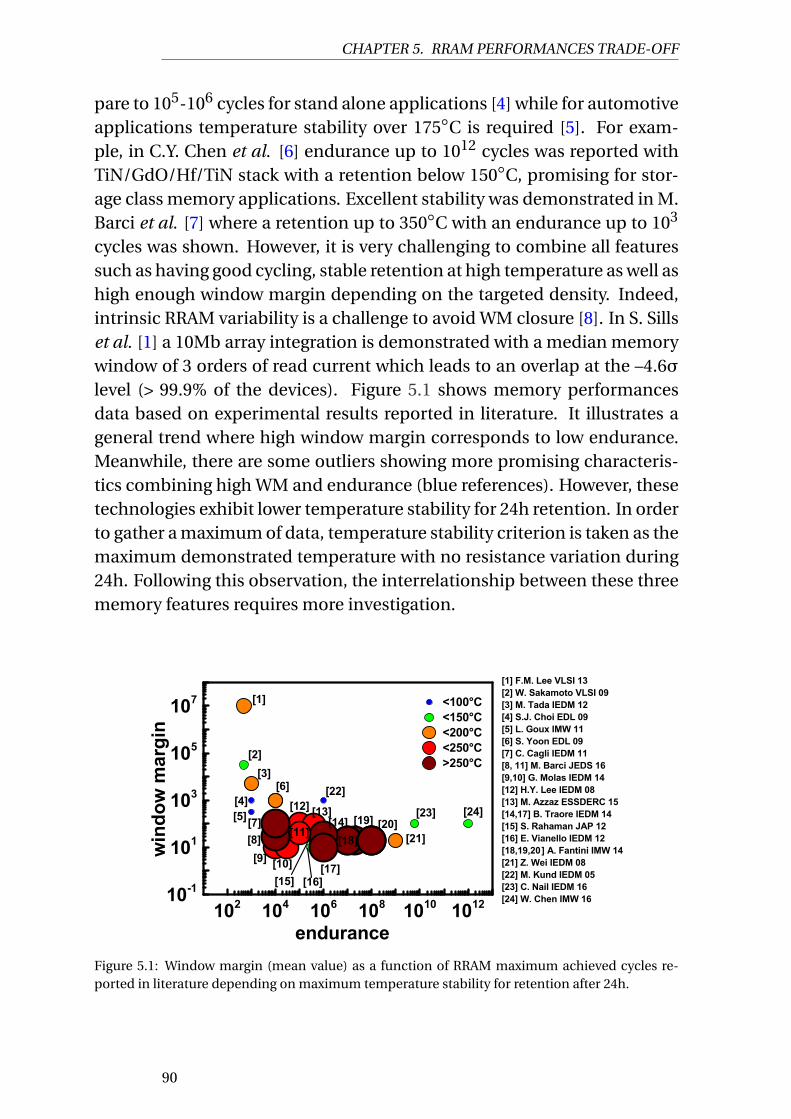
CHAPTER 5. RRAM PERFORMANCES TRADE-OFF
pare to 105-106 cycles for stand alone applications [4] while for automotiveapplications temperature stability over 175C is required [5]. For exam-ple, in C.Y. Chen et al. [6] endurance up to 1012 cycles was reported withTiN/GdO/Hf/TiN stack with a retention below 150C, promising for stor-age class memory applications. Excellent stability was demonstrated in M.Barci et al. [7] where a retention up to 350C with an endurance up to 103
cycles was shown. However, it is very challenging to combine all featuressuch as having good cycling, stable retention at high temperature as well ashigh enough window margin depending on the targeted density. Indeed,intrinsic RRAM variability is a challenge to avoid WM closure [8]. In S. Sillset al. [1] a 10Mb array integration is demonstrated with a median memorywindow of 3 orders of read current which leads to an overlap at the –4.6σlevel (> 99.9% of the devices). Figure 5.1 shows memory performancesdata based on experimental results reported in literature. It illustrates ageneral trend where high window margin corresponds to low endurance.Meanwhile, there are some outliers showing more promising characteris-tics combining high WM and endurance (blue references). However, thesetechnologies exhibit lower temperature stability for 24h retention. In orderto gather a maximum of data, temperature stability criterion is taken as themaximum demonstrated temperature with no resistance variation during24h. Following this observation, the interrelationship between these threememory features requires more investigation.
102 104 106 108 1010 101210-1
101
103
105
107[1] F.M. Lee VLSI 13[2] W. Sakamoto VLSI 09[3] M. Tada IEDM 12[4] S.J. Choi EDL 09[5] L. Goux IMW 11[6] S. Yoon EDL 09[7] C. Cagli IEDM 11[8, 11] M. Barci JEDS 16[9,10] G. Molas IEDM 14[12] H.Y. Lee IEDM 08[13] M. Azzaz ESSDERC 15[14,17] B. Traore IEDM 14[15] S. Rahaman JAP 12[16] E. Vianello IEDM 12[18,19,20] A. Fantini IMW 14[21] Z. Wei IEDM 08[22] M. Kund IEDM 05[23] C. Nail IEDM 16[24] W. Chen IMW 16
[15]
[20][19]
[18]
[17][16]
[14][13][12]
[11]
[10][9][8][7]
[21]
[24][23]
[22][6]
[5][4]
[1]
[3]
<100°C<150°C<200°C<250°C>250°C
win
dow
mar
gin
endurance
[2]
Figure 5.1: Window margin (mean value) as a function of RRAM maximum achieved cycles re-ported in literature depending on maximum temperature stability for retention after 24h.
90

CHAPTER 5. RRAM PERFORMANCES TRADE-OFF
5.3 Optimizing programming conditions
Our measurements are done on different RRAM samples with a BE / Oxide/ CuTexGey structure (see Figure 5.2). The memory is integrated in 1T1Rconfigurations using a CMOS transistor as selector. 3nm to 3.5nm of amor-phous a-Al2O3 [9] or 5nm of amorphous a-HfO2 [10] or 4nm of GdOx [11]was deposited by PVD or ALD on different PVD bottom electrode (TiN, W).20nm of CuTexGey deposited by PVD was used as top electrode (TE). Fig-ure 5.2 shows TEM cross section of W/HfO2/CuTex RRAM developed inthis work using a plug structure.
3.5nmAl2O3
CuTex
WSiN
CuTex
W
HfO2
CuWHf
5nmTop Electrode
oxide
Bottom Electrode
3nmAl2O3
CuTex
TiN
5nm HfO2
CuTex
W
4nm GdOx
CuTex
TiN
Figure 5.2: Schematic of the RRAM technologies studied in this work with TEM cross sections ofW/HfO2/CuTex based CBRAM, and EDX (Hf, W, Cu) images.
In order to study our RRAM, we first optimize programming conditionsand observe their impact on memory characteristics. Focusing on TiN /Al2O3 / CuTex samples, Figure 5.3a shows SET programming current de-pending on window margin. Increasing the SET current to 100µA improvesthe window margin. Above that, WM is degraded due to high electric stressapplied to the dielectric, reducing the OFF state resistance after RESET op-eration. Figure 5.3b shows pulse length for SET and RESET impact. De-creasing pulse lenght reduces WM, but increases speed and decreases con-sumption. A typical endurance can be seen in Figure 5.3c at 100µA with itsassociated resistance distribution in Figure 5.3d.
91

CHAPTER 5. RRAM PERFORMANCES TRADE-OFF
(a)
30 60 90 120 1500
100
200
300 Degradation
Mea
n R
off/R
on
Ic[µA]
Optimum Ic
(b)
0 300 600 900 12000
100
200
300
Mea
n R
off/R
on
tpulse[ns](c)
102 104 106 108103104105106107108
R [o
hm]
100µA
cycles
Ncmax
(d)
104 105 106 107 1080.011
10407095
99.5
Mean valuePr
obab
ility
[%]
R[ohm]
Figure 5.3: (a) Summary of WM behavior depending on SET current Ic and programming timetprog. Low Ic offers low window margin while high Ic (150µA) degrades ROFF b) Long tprog improvesthe window margin at the expense of lower speed and degraded consumption c) and d) Endurancecharacteristics of TiN / Al2O3 / CuTex RRAM at 100µA with cycle to cycle Resistance distribution(tSET=tRESET=1µs). Error bars correspond to standard deviation measured on 100 subsequent cy-cles.
5.4 Endurance vs Window Margin Trade-off
In order to study the trade-off between WM and endurance, we extract themaximum number of cycles a cell can reach for different RESET voltages(VRESET), giving different WM, setting time pulse at 1µs. The maximumnumber of cycles (Ncmax) is achieved when RESET operation becomes im-possible, meaning oxide layer was led to an irreversible breakdown (seeFigure 5.3c), leading to window margin closure. Figure 5.4b and Figure 5.4cshow VRESET influence on ROFF and endurance respectively. Figure 5.4ashows typical curves to extract these data. ROFF increases with VRESET untila threshold value is reached where WM is then degraded. WM degradationafter 2V can be explained by a negative SET following the RESET due to de-fect injection from the BE [12]. On the other hand, the maximum number
92

CHAPTER 5. RRAM PERFORMANCES TRADE-OFF
of cycles decreases as VRESET increases. Results reveal a trade-off betweenWM and endurance: staying out of an early degradation with VRESET belowa threshold value, improving WM leads to a degraded endurance.
Vr=1.9VVr=2.1V
Vr=2.9V
a)
1.0 1.5 2.0 2.5 3.0104
105
106
107
108b)
Rof
f [oh
m]
Vreset [V]
early degradation
1.0 1.5 2.0 2.5 3.010-1
101
103
105
107c)
endu
ranc
e
Vreset [V]
Figure 5.4: a) Typical endurance curves with different VRESET to extract b) and c). Impact of VRESETon TiN/Al2O3/CuTex sample on b) ROFF, error bars corresponds to standard deviation on 10 cellsand c) endurance (maximum number of achieved cycles).
5.5 Endurance plus Window Margin improvement vs reten-tion Trade-off
In order to compare different materials, this study is extended to 4 RRAMtechnologies. We chose to fix the programming current to 100µA, which isclose to the optimum programming current insuring large WM and highnumber of cycles. Taking the RESET parameter giving the best endurancefor each technology, we compared their endurance (Ncmax) and their bestretention (highest stability temperature T
max for 24h baking time). Resultsare shown in Figure 5.5 for three of them. W/HfO2/CuTex shows up to6.109 cycles with a constant WM while its maximum temperature stabilityis around 100C. TiN / Al2O3 / CuTex shows an endurance up to 107 anda temperature stability up to 200C while TiN/GdOx/CuTex shows an en-durance up to 3.103 and a stable retention up to 300C. These three RRAMare a good example to illustrate the trade-off between endurance and re-
93

CHAPTER 5. RRAM PERFORMANCES TRADE-OFF
tention: good cycling goes with poor retention (W/HfO2/CuTex technol-ogy), while stable retention is reached at the cost of limited endurance(TiN/GdOx/CuTex technology). Figure 6.1a represents reached endurancefor each RRAM technology for different RESET Voltage conditions, imply-ing different WM. Focusing on one material, WM can be increased at theexpense of degraded endurance. Having compared different materials (fora given WM), it can be concluded that endurance is improved as reten-tion is degraded (Figure 6.1b). Through these results, trade-off betweenendurance, WM and retention is revealed.
(a) (b) (c)
102 104 106 108 1010 1012103
104
105
106
107
108
R [o
hm]
cycles102 104 106 108103
104
105
106
107
108
R [o
hm]
cycles100 101 102 103103
104
105
106
107
108
R[ohm
]
cycles
10-1 101 103 105 107103
104
105
106
107
108
R [o
hm]
t [s]
100°C
100 101 102 103 104 105103
104
105
106
107
108
R [o
hm]
t [s]
200°C
10-1 101 103 105103
104
105
106
107
108
R[ohm
]
t [s]
300°C
Figure 5.5: Endurance and retention performances for a) W/HfO2/CuTex, b) TiN/Al2O3/CuTex
and c) TiN/GdOx/CuTex memory technologies.
94

CHAPTER 5. RRAM PERFORMANCES TRADE-OFF
(a)
101 103 105 107 109 1011101
102
103
TiN/Al2O3
TiN/GdOx
W/HfO2
W/Al2O3
max endurance (# cycles)
mea
n R
off/R
on(b)
102 104 106 108 1010
100150200250300
max
sta
bilit
y T
[°C
]
max endurance (# cycles)
TiN/GdOx
W/Al2O3
TiN/Al2O3
W/HfO2
Figure 5.6: a) Window Margin as function of maximum endurance. For each RRAM technology,various WM were achieved changing the RESET conditions. Gray line is used to extract b) fora constant WM. b) Maximum stable retention temperature after 24h baking time as function ofmaximum endurance for a given WM (ROFF/RON ∼400).
5.6 RRAM Filament properties
To go further, endurance, WM, retention trade-off is studied from a mate-rial point of view. Atomistic simulations are performed to study the differ-ent oxides. In this section, the objective is to analyze the filament compo-sition of the various investigated memory stacks, and to extract the micro-scopic material properties, in particular the energy required to diffuse ionsduring filament formation. To avoid redundancy, we will only present thedetailed calculations for HfO2/Cu RRAM.
5.6.1 Simulation framework
For hafnia, a 96-atoms supercell consisting of eight monoclinic-HfO2 unitcells was calculated. This structure is the closest crystalline form of ouramorphous PVD material with a density of 9.8g.cm–3 vs the measurementvalue of 10g.cm–3. Different positions were tested for each defect, espe-cially for interstitials, up to 4 inequivalent sites were compared (see Fig-ure 5.7). Detailed calculation parameters can be found in Annexe.
The band gap obtained at 3.73eV is corrected [13] in G0W0 at 5.2eV vs5.5eV measured by ellipsometry. For the TE we used a 96-atom supercellconsisting of eight Cu2Te3Ge unit cells [14]. This structure is the clos-est crystalline form of our amorphous PVD material with a density of 6.0g.cm–3 vs 6.1 g.cm–3 (measured). All results are based on a band alignmentbetween the band-gap of hafnia and Cu2Te3Ge which was done consider-ing
95

CHAPTER 5. RRAM PERFORMANCES TRADE-OFF
Figure 5.7: HfO2 and a – HfO2 structure with different copper interstitial positions. O in red, Hf inblue, Cu in orange. Cui1 and Cui2 are used for migration barrier calculation.
• G0W0 gap correction with an opening of 1eV at the conduction bandand -0.5 eV at the valence band.
• Electron affinity of HfO2 at 2eV [15]
To complete the study, an amorphous a-HfO2 model with a density of9.4g.cm–3 was implemented. This model was generated using the meltand quench method: a crystalline monoclinic-HfO2 with Schottky defectswas used for the initial structure to lower density with the eight HfO2 unitcells considered above. It was melted at 2800K for 10ps and cooled to 300Kfor 10ps with a time step of 1fs. 1 k-point was used during the moleculardynamics while 2*2*2k-points were used for the defect calculations. Theband gap is obtained at 3eV free of defect against 3.73eV in the crystallinestructure.
5.6.2 HfO2 thermodynamic of defects
We studied HfO′2 s point defects in contact with a CuTex-based TE. As we
consider exchanges between HfO2 and CuTe2Ge3, calculations are basedon the following equation for an interstitial of copper charged +q (Cu+q
i ):
∆H = UHfO2:Cu+qi
– UHfO2 + UCuTe2Ge3:VCu – UCuTe2Ge3
+q · (EFermi +∆V + EVB)(5.1)
With ∆H the formation enthalpy of the defect, UDefect the total energyof the defect, UPristine the total energy of the initial state, ni and µi thenumber of chemical formula and the reference chemical potential for theexchange, q the charges exchanged in the system, EFermi the Fermi level ofthe electrode in considered contact, ∆V the electrostatic energy shift[16]
96

CHAPTER 5. RRAM PERFORMANCES TRADE-OFF
and EVB the highest valence band energy level. Results are presented inFigure 5.8 and Figure 5.9 with the lowest charged defects. Considering thecharge of the species and a top electrode in contact based on Cu (verti-cal orange line), the most favorable interstitials and vacancies we couldobtain are respectively: Copper interstitial (Cu+1
i ), Oxygen Vacancy (V+2O ).
Tellurium interstitial and hafnium vacancies are not considered here be-cause of their high formation enthalpy energy. As explained in the pre-vious chapter, Ge is used to stabilize CuTe layer and keep it amorphousduring integration process, to prevent any segregation and phase separa-tion. Typically, 10-20% Ge is used [17, 18] in CuTe alloys. As a consequence,Ge is not expected to have any impact in the electrical behaviour of CuTe.Moreover, CuTe bound is polar and can easily be broken in Cuδ+ and Teγ–
ions. They will be mobile under the electric field. Ge calculations are justused to confirm this affirmation. We will thus focus on Cu ions in the nextsections.
0 1 2 3 4 5-202468
10
VHf-4
Cui0 VO
-2VO0VO
+1
VO+2
Cui-2
Cui-1
Cui+1
Cui+2
W-Cu
H
[eV]
Electrode Fermi level relative to HfO 2 BandGap [eV]
Pt Ti-Al
Figure 5.8: Formation enthalpy calculation of defects in HfO2/CuTexGey system. Fermi level of 3types of metal (Pt, W-Cu, Ti-Al) is represented (dashed vertical lines).
Based on these two candidates, we studied the case of copper introduc-tion in defective hafnia. The reference for the oxide becomes then a VO-rich HfO2 (HfO2 with one VO defect) instead of stoichiometric HfO2. VO inHfO2 can come from
• HfO2 process condition in O-poor atmosphere
• O exchange with the TE during forming process requiring 4.8eV.
The results are summarized Table 5.1 and based on the following equa-tion:
97

CHAPTER 5. RRAM PERFORMANCES TRADE-OFF
0 1 2 3 4 5-202468
10
Gei-1
Gei0
Gei+2
Gei+3
Tei+2
Tei+3
Tei-1
Tei0
W-Cu
H
[eV]
Electrode Fermi level relative to HfO 2 BandGap [eV]
Pt Ti-Al
Figure 5.9: Formation enthalpy calculation of defects in HfO2/CuTexGey system. Fermi level of 3types of metal (Pt, W-Cu, Ti-Al) are represented (dashed vertical lines).
∆H = UHfO2:VO+Cu+qi
– UHfO2:VO+ UCuTe2Ge3:VCu
–UCuTe2Ge3 + q · (EFermi +∆V + EVB)(5.2)
Table 5.1: Formation enthalpy ∆H (eV) between the TE and HfO2 either stoichiometric or includ-ing oxygen vacancies
Defect ∆H HfO2 (eV) ∆H VO-rich (eV)
Cu+1i 3.4 2.6
V+2O 4.8 x
V–4Hf 9.1 x
OFP 4.5 x
Te+2i 9.1 x
Ge+2i 5.6 x
Cu introduction is favorable in interstitial site while if HfO2 is VO rich,Cu introduction is the easiest in the interstitial site next to VO.
To complete these results, same calculations were performed in amorphous-HfO2 (see structure Figure 5.7). Up to 6 positions were tested for each de-fect. Table 5.2 reports the most favorable ones. The results are similar tocrystalline HfO2 allowing to pursue the calculation only with this structureto optimize calculation time. It can be noted that formation energies arelower in amorphous structure which show
98

CHAPTER 5. RRAM PERFORMANCES TRADE-OFF
Table 5.2: Formation enthalpy(∆H) in a-HfO2 stoichiometric or VO-rich calculated in GGA con-sidering exchanges with a Cu2Te3Ge Top Electrode
Defect ∆H HfO2 (eV) ∆H VO-rich-HfO2 (eV)
Cu+1i 1.8 1.4
V+2O 5.9 x
5.6.3 HfO2 defect diffusion
The most favorable defects that can be inserted in HfO2 were extracted.However, thermodynamic approach only considers initial and final energystates of the defects. Therefore, this section focuses on Cu diffusion toquantify the energetic barrier height to move it between two equivalentsites. Energy migration barriers are calculated using NEB-based (NudgedElastic Band) approaches. The presented results correspond to Cu migra-tion from Cui1 site to Cui2 (see Figure 5.7).
The diffusion barrier of Cu+i in HfO2 structure was found close to 2.5eV
(Figure 5.10). We also calculated Cu migration barriers in defective hafniastructures with a VO next to the Cu migration path. In particular, the diffu-sion barriers of Cu+
i in HfO2-VO is evaluated at 1.28eV. Cu can pass througha CuO state. To complete this result, calculations were performed on theamorphous modele. The diffusion barrier of Cu+
i in a-HfO2 is found closeto 3eV and 2.5eV with Cu+
i next to VO.
0 2 4 6 8 10 12-0.50.00.51.01.52.02.53.03.5
Cui +1
Cui +1 next to VO
Cui +1 a-HfO2
E [ e
V ]
d [ Å ]
Ea
dh
Figure 5.10: First principle calculations to compute the barrier height to diffuse from Cui1 to Cui2sites (see Figure 5.7): Cu+1
i diffusion barrier in stoichiometric or defective HfO2 systems.
99

CHAPTER 5. RRAM PERFORMANCES TRADE-OFF
5.6.4 Simulation results summary
This study is done for 3 different materials: Al2O3, HfO2 and Gd2O3. Ta-ble 6.1 summarizes the main results. If thermodynamic and kinetic en-ergies are taken into account, Al2O3 and Gd2O3 show (CuiVO)+1 defect asthe most favorable while HfO2 shows favorable energies for (CuiVO)+1 andV+2
O .
Table 5.3: Migration energy barrier, Ea, and formation enthalpy, ∆H, between the TE and differentoxides either stoichiometric or including oxygen vacancies (CuiVO defect).
Defect ∆HHfO2 (eV) Ea HfO2 (eV) ∆HAl2O3 (eV) Ea Al2O3 (eV) ∆HGdOx (eV) Ea GdOx (eV)
Cu+1i 3.4 2.5 2.5 4 3.5 2
VxO 2.5 (+2) 0.7 (+2) 3.8 (0) 3.5 (0) 4.1 (0) x
(CuiVO)+1 2.6 1.3 0.6 1.4 1.2 3.44
Filament Hybrid: Cui and VO moving Cui next to VO Cui next to VO
5.7 A link between RRAM performances and material mi-croscopic properties
5.7.1 Migration energy barrier correlated to RRAM performances
Combining electrical characterization and DFT results, we can put in evi-dence a clear correlation between memory characteristics and the ion mi-gration barrier. Figure 5.11 represents memory endurance and retentiontemperature as a function of calculated Emigration. The number of cyclesreachable by a cell decreases with Emigration (Figure 5.11a) while temper-ature stability increases (Figure 5.11b). This phenomenon can be under-stood with a simple description of ion migration in the resistive layer. Fig-ure 5.11 illustrates how endurance is facilitated by a low migration barrier;a low energy will lead to an easy formation and disruption of the filament.A high migration energy barrier will lead to stable retention; making thefilament more difficult to be dissolved. In HfO2, as CuiVO and VO calcu-lated migration energies are of the same order of magnitude (see Table 6.1),we considered a hybrid filament resulting from both Cu and VO diffusion.Thus, Emigration is calculated as the average value between CuiVO and VOin Figure 5.11. In conclusions, it clearly appears that the ion migration en-ergy is linked to the trade-off between memory endurance and retention.It can be noted that there is no clear correlation found with the formationenthalpy energies (see Figures 5.12a and 5.12b).
100
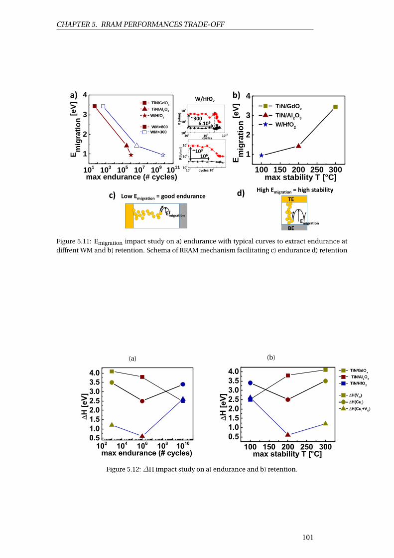
CHAPTER 5. RRAM PERFORMANCES TRADE-OFF
101
103
105
107
109
1011
1
2
3
4
Em
igra
tio
n [e
V]
max endurance (# cycles)
TiN/GdOx
TiN/Al2O
3
W/HfO2
WM>800
WM>300
100 150 200 250 300
1
2
3
4
Em
igra
tio
n [e
V]
max stability T [°C]
TiN/GdOx
TiN/Al2O
3
W/HfO2
102
107
103
105
107
R [
oh
m]
cycles
Low Emigration = good endurance
Emigration
Emigration
TE
BE
High Emigration = high stability
W/HfO2
102
107
1012
103
105
107
R [
oh
m]
cycles
~3006.109
~103
106
a) b)
c) d)
Figure 5.11: Emigration impact study on a) endurance with typical curves to extract endurance atdiffrent WM and b) retention. Schema of RRAM mechanism facilitating c) endurance d) retention
(a)
102 104 106 108 10100.51.01.52.02.53.03.54.0
H [e
V]
max endurance (# cycles)
(b)
100 150 200 250 3000.51.01.52.02.53.03.54.0
H [e
V]
max stability T [°C]
TiN/GdOx
TiN/Al2O3
TiN/HfO2
H(VO) H(Cui) H(Cui+VO)
Figure 5.12: ∆H impact study on a) endurance and b) retention.
101

CHAPTER 5. RRAM PERFORMANCES TRADE-OFF
5.7.2 Qualitative explanation
To discuss in more details the previous observation, we propose the fol-lowing description: a RRAM device can be characterized by a maximumenergy, Emax, that can be sustained before oxide degradation and break-down. This maximum energy is reached when a maximum number of cy-cles, Ncmax, is achieved. RRAM is then led to irreversible breakdown. Foreach cycle, provided energy, Ecycle, depends on the programming condi-tions. The maximum energy can thus be expressed with Ncmax and Ecycle(Equation (5.3)a). A fraction of Ecycle is transferred to ions and serves toswitch the RRAM (Eswitch) while another is transferred to the network andleads to material degradation such as defect generation. In our case, en-durance failure is detected when RRAM can not be erased anymore. Thecell is then stuck in Ron state meaning there are too much defects in theoxide which leads to a permanent conductive path. Creation of defects oc-curs during cycling and can be accelerated by the increase of VRESET [12].
As it was previously demonstrated, increasing ROFF/RON ratio leads to adrop in the number of cycles a cell can sustain. Thus, the maximum energyis reached faster if WM increases. In our description, we link the WM tothe number of atoms involved during filament formation and disruption(Nmoved atoms). Increasing SET programming condition leads to biggerconductive path, then composed of more atoms and resulting in lower RONand higher WM. However, increasing ROFF means a bigger free defect areain resistive layer meaning that increasing RESET condition (time and volt-age) is equivalent to increase the number of moving atoms during RESET.On the other hand, we also demonstrated that ion migration barrier im-pacts memory endurance. If Emigration increases, the number of achievedcycle decreases. In our description, we thus assume that Emigration is therequired energy to move and drift each ion in the oxide, during filamentformation and disruption. So, switching energy can be expressed as Eswitch= Emigration * Nmoved atoms. The maximum energy of the dielectric canthus be expressed with the maximum number of cycles, the WM (throughNmoved atoms) and Emigration. In S. Balatti et al. [12] a similar descriptionof this phenomenon is given. Degradation of the oxide is controlled by ac-tivation energy and VRESET. Irreversible endurance failure is associated toa high defect injection in conductive filament.
As explained previously, the switching energy (transferred to filamentions) only represents a fraction of the total supplied energy. Energy sur-plus is transferred to the network and degrades the oxide. We can expressthe total provided energy with Eswitch and a degradation parameter α with
102

CHAPTER 5. RRAM PERFORMANCES TRADE-OFF
Eswitch=α*Ecycle, 0 < α < 1. α evolves with oxide degradation: the more theRRAM is cycled, the more the oxide is degraded, leading to a higher en-ergy amount transferred to the network. We thus assume α = 1 for a freshcell (without defect) and gradually decreases with cycling. Finally we canexpress the maximum energy that the dielectric can sustain depending onNcmax, Eswitch and α (see 5.3).
Emax ∝ Ncmax∗Ecycle (5.3a)
Ecycle ∝Eswitch
α∝ Emigration∗Nmoved atoms
α(5.3b)
Emax ∝ Ncmax∗Emigration∗Nmoved atoms
⇓ ⇓ ⇓Endurance Retention WM
(5.4)
Where Emax the maximum energy a dielectric can sustain before break-down, Ncmax the maximum number of achieved cycles, Ecycle the total en-ergy supplied per cycle, Eswitch the energy needed to move the atoms tocreate the filament, α the degradation parameter such as Eswitch=α*Ecycleand 0 < α < 1, Emigration the activation energy to move one atom in theoxide and Nmoved atoms the number of involved atoms in the filament for-mation and disruption.
5.7.3 Impact on RRAM material choice
In parallel, Emigration can be associated to the activation energy experi-mentally extracted from retention measurements. Figure 5.14a shows cor-relations between simulated and experimental Emigration and memory en-durance. Very good agreement is observed between simulated and experi-mental Emigration. Temperature stability failure can then be well associatedwith movement of Cu and VO atoms which will disrup or form again the fil-ament [19]. ROFF failure, on Figure 5.14b, reveals a filament formation.
In conclusion, the maximum dielectric energy is linked to the memoryperformances and microscopic features of the memory technology: win-dow margin (through the number of atoms involved in the filament for-mation and disruption), memory endurance (maximum number of cycles)and memory retention (through ion migration barrier). Consequently:
• Stronger programming conditions (current, time or voltage) enlargethe WM, decreasing Ncmax (and endurance) for a given memory tech-nology (fixed Emax), as observed in Figure 6.1a.
103

CHAPTER 5. RRAM PERFORMANCES TRADE-OFF
102 104 106 108 1010 10120
1
2
3
4
E mig
ratio
n [e
V]
max endurance (# cycles)
TiN/GdOx
W/Al2O3
TiN/Al2O3
W/HfO2
Esimulation
Eexperimental
Figure 5.13: Migration energy barrier experimental and simulated as a function of maximum en-durance.
Figure 5.14: Extraction example of Eexperimental for W/HfO2).
• Changing memory stack, it makes possible to tune the migration en-ergy and favor either endurance or retention (Figure 6.1b, and Fig-ure 5.11), for a fixed window margin.
Following observations must also be made:
• Dielectric optimization is of great importance; improving the mate-rial quality can lead to Emax increase and general improvement ofthe WM/endurance/retention trade-off. In literature, J. Woo et al.demonstrated that breakdown strenght of a material can be improvedby thermal treatment [20].
• Top Electrode/oxide combination needs to be optimized to tune mi-gration barrier. Unfortunately, this study needs to be done for eachcombination. However, some guidance can be given to avoid high
104

CHAPTER 5. RRAM PERFORMANCES TRADE-OFF
diffusion in oxides such as: controlling oxide grain boundaries, mate-rial structure and material density. It can be added that small metalatoms is an advantage for interstitial diffusion which is usually themost favorable.
• Understanding the defect generation during memory endurance isalso critical. For a given window margin, different sets of program-ming parameters (current, time, voltage. . . ) and memory stack fea-tures (top, bottom electrodes. . . ) should minimize endurance failure,preventing early oxide degradation (Figure 5.4). Moreover, smart pro-gramming procedures is a way to adjust the energy provided to thesystem, reducing the energy surplus transferred to the network anddegrading the memory dielectric.
The link between memory technology microscopic features and mem-ory performances can be used to design an optimized memory stack. How-ever, operating conditions need to be adjusted to reach the specificationsof a given memory application. Figure 6.2 summarizes optimization forthree applications. Low migration barrier and optimized WM favor en-durance for Storage Class Memory (proposed stack: W/HfO2/CuTex). Op-timized SET current and long time programming conditions enlarge WMfor data storage (proposed stack: TiN/Al2O3/CuTex). High migration bar-rier and large WM are favorable for embedded applications requiring highstability (proposed stack: TiN/GdOx/CuTex).
5.8 Chapter V synthesis
In this chapter, we studied the trade-off between RRAM performances.Compromise between endurance and window margin is exposed for onetechnology. Increasing window margin changing SET and RESET condi-tion lead to a degraded endurance. Comparing different devices, a linkbetween retention and endurance vs WM improvement is presented. For agiven WM, improving retention leads to a degraded endurance. Atomisticsimulations are then used to bring insight from a material point of view. Inparticular, the ion migration barrier is correlated to the endurance/retentioncompromise. It can be tuned by TE/oxide combinaison and material en-gineering. Window margin improvement, changing the SET RESET condi-tions, degrades endurance. The optimization of the dielectric quality is away to improve the overall window margin/retention/endurance compro-mise. Based on the understanding of the filament composition and char-
105

CHAPTER 5. RRAM PERFORMANCES TRADE-OFF
acteristics, various memory technologies are proposed to reach the speci-fications of different memory applications.
Figure 5.15: Radar plot of the performance trade-off for the various RRAM classes reported in thiswork, and critical key parameters (material microscopic properties and operating conditions).
106

Bibliography
[1] S. Sills, S. Yasuda, J. Strand, A. Calderoni, K. Aratani, A. Johnson,and N. Ramaswamy. A copper ReRAM cell for Storage Class Mem-ory applications. In 2014 Symposium on VLSI Technology (VLSI-Technology): Digest of Technical Papers, pages 1–2, June 2014. doi:10.1109/VLSIT.2014.6894368. 89, 90
[2] J. R. Jameson, P. Blanchard, C. Cheng, J. Dinh, A. Gallo, V. Gopalakr-ishnan, C. Gopalan, B. Guichet, S. Hsu, D. Kamalanathan, D. Kim,F. Koushan, M. Kwan, K. Law, D. Lewis, Y. Ma, V. McCaffrey, S. Park,S. Puthenthermadam, E. Runnion, J. Sanchez, J. Shields, K. Tsai,A. Tysdal, D. Wang, R. Williams, M. Kozicki, J. Wang, V. Gopinath,S. Hollmer, and M. Van Buskirk. Technical Digest - International Elec-tron Devices Meeting, IEDM. 2013. doi: 10.1109/IEDM.2013.6724721.89
[3] Z. Wei, K. Eriguchi, S. Muraoka, K. Katayama, R. Yasuhara, K. Kawai,Y. Ikeda, M. Yoshimura, Y. Hayakawa, K. Shimakawa, T. Mikawa, andS. Yoneda. Distribution projecting the reliability for 40 nm ReRAMand beyond based on stochastic differential equation. In 2015 IEEEInternational Electron Devices Meeting (IEDM), pages 7.7.1–7.7.4, De-cember 2015. doi: 10.1109/IEDM.2015.7409650. 89
[4] ITRS. Executive Report, 2015. 90
[5] R. Strenz. Embedded Flash technologies and their applications: Sta-tus amp; outlook. In 2011 International Electron Devices Meeting,pages 9.4.1–9.4.4, December 2011. doi: 10.1109/IEDM.2011.6131521.90
[6] C. Y. Chen, L. Goux, A. Fantini, A. Redolfi, G. Groeseneken, and M. Ju-rczak. Doped Gd-O Based RRAM for Embedded Application. In2016 IEEE 8th International Memory Workshop (IMW), pages 1–4, May2016. doi: 10.1109/IMW.2016.7495266. 90
107

BIBLIOGRAPHY
[7] M. Barci, J. Guy, G. Molas, E. Vianello, A. Toffoli, J. Cluzel, A. Roule,M. Bernard, C. Sabbione, L. Perniola, and B. D. Salvo. Impact of SETand RESET conditions on CBRAM high temperature data retention. In2014 IEEE International Reliability Physics Symposium, pages 5E.3.1–5E.3.4, June 2014. doi: 10.1109/IRPS.2014.6860677. 90
[8] A. Fantini, L. Goux, R. Degraeve, D. J. Wouters, N. Raghavan,G. Kar, A. Belmonte, Y. Y. Chen, B. Govoreanu, and M. Jurczak.Intrinsic switching variability in HfO2 RRAM. In 2013 5th IEEEInternational Memory Workshop, pages 30–33, May 2013. doi:10.1109/IMW.2013.6582090. 90
[9] C. Nail, P. Blaise, G. Molas, M. Bernard, A. Roule, A. Toffoli, L. Perniola,and C. Vallée. Atomistic mechanisms of copper filament formationand composition in Al2o3-based conductive bridge random accessmemory. Journal of Applied Physics, 122(2):024503, July 2017. doi:10.1063/1.4990979. 91
[10] C. Nail, G. Molas, P. Blaise, G. Piccolboni, B. Sklenard, C. Cagli,M. Bernard, A. Roule, M. Azzaz, E. Vianello, C. Carabasse, R. Berthier,D. Cooper, C. Pelissier, T. Magis, G. Ghibaudo, C. Vallée, D. Be-deau, O. Mosendz, B. D. Salvo, and L. Perniola. UnderstandingRRAM endurance, retention and window margin trade-off using ex-perimental results and simulations. In 2016 IEEE International Elec-tron Devices Meeting (IEDM), pages 4.5.1–4.5.4, December 2016. doi:10.1109/IEDM.2016.7838346. 91
[11] M. Barci, G. Molas, C. Cagli, E. Vianello, M. Bernard, A. Roule, A. Tof-foli, J. Cluzel, B. D. Salvo, and L. Perniola. Bilayer Metal-Oxide Con-ductive Bridge Memory Technology for Improved Window Marginand Reliability. IEEE Journal of the Electron Devices Society, 4(5):314–320, September 2016. doi: 10.1109/JEDS.2016.2567219. 91
[12] S. Balatti, S. Ambrogio, Z. Q. Wang, S. Sills, A. Calderoni, N. Ra-maswamy, and D. Ielmini. Pulsed cycling operation and endurancefailure of metal-oxide resistive (RRAM). In 2014 IEEE InternationalElectron Devices Meeting, pages 14.3.1–14.3.4, December 2014. doi:10.1109/IEDM.2014.7047050. 92, 102
[13] L. G. Ferreira, M. Marques, and L. K. Teles. Approximation to den-sity functional theory for the calculation of band gaps of semicon-ductors. Physical Review B, 78(12):125116, September 2008. doi:http://link.aps.org/doi/10.1103/PhysRevB.78.125116. 95
108

BIBLIOGRAPHY
[14] G. E. Delgado, A. J. Mora, M. Pirela, A. Velásquez-Velásquez, M. Vil-larreal, and B. J. Fernández. Structural refinement of the ternarychalcogenide compound Cu2gete3 by X-ray powder diffraction. phys-ica status solidi (a), 201(13):2900–2904, October 2004. doi: http://onlinelibrary.wiley.com/doi/10.1002/pssa.200406850/abstract. 95
[15] W. Zheng, K. H. Bowen, J. Li, I. Daabkowska, and M. Gutowski. Elec-tronic Structure Differences in ZrO2 vs HfO2. The Journal of Phys-ical Chemistry A, 109(50):11521–11525, December 2005. doi: http://dx.doi.org/10.1021/jp053593e. 96
[16] C. Freysoldt, B. Grabowski, T. Hickel, J. Neugebauer, G. Kresse, A. Jan-otti, and C. G. Van de Walle. First-principles calculations for point de-fects in solids. Reviews of Modern Physics, 86(1):253–305, March 2014.doi: http://link.aps.org/doi/10.1103/RevModPhys.86.253. 96
[17] W. Devulder, K. Opsomer, M. Jurczak, L. Goux, and C. Detav-ernier. Influence of alloying the copper supply layer on the re-tention of CBRAM. In 2015 IEEE International Interconnect Tech-nology Conference and 2015 IEEE Materials for Advanced Metal-lization Conference (IITC/MAM), pages 215–218, May 2015. doi:10.1109/IITC-MAM.2015.7325623. 97
[18] K. Ohba, S. Yasuda, T. Mizuguchi, K. Aratani, M. Shimuta,A. Kouchiyama, and M. Ogasawara. Memory component, mem-ory device, and method of operating memory device, August2011. U.S. Classification 365/148, 257/2, 257/4, 257/E45.003;International Classification H01L45/00, G11C11/00; Cooper-ative Classification G11C11/161, H01L45/145, H01L45/1253,H01L45/1233, H01L45/1633, H01L45/146, H01L45/1266,H01L45/085, H01L27/2472, H01L27/2436, G11C13/0011, G11C11/16;European Classification H01L45/12E4, H01L45/14C2, H01L45/14C,H01L27/24F, H01L45/08M, H01L27/24H2, H01L45/16D6,G11C13/00R5B. 97
[19] J. Guy, G. Molas, C. Cagli, M. Bernard, A. Roule, C. Carabasse, A. Tof-foli, F. Clermidy, B. D. Salvo, and L. Perniola. Guidance to reliabilityimprovement in CBRAM using advanced KMC modelling. In 2017IEEE International Reliability Physics Symposium (IRPS), pages PM–2.1–PM–2.5, April 2017. doi: 10.1109/IRPS.2017.7936384. 103
[20] J. Woo, A. Belmonte, A. Redolfi, H. Hwang, M. Jurczak, and L. Goux.Introduction of WO3 Layer in a Cu-Based Al2o3 Conductive Bridge
109

BIBLIOGRAPHY
RAM System for Robust Cycling and Large Memory Window. IEEEJournal of the Electron Devices Society, 4(3):163–166, May 2016. doi:10.1109/JEDS.2016.2526632. 104
110

Chapter 6
Synthesis and perspectives
6.1 Objectives
Through this research work, electrical characterization combining withatomistic simulation allowed to improve filament formation understand-ing involved in HRRAM operation. However, a global physical compre-hension of RRAM working principle is still lacking. This research workaims to offer a first approach to HRRAM physical mechanism, studyingmaterial stack parameters and electrical characteristics. Deep results onAl2O3/Cu based-HRRAM were presented giving insight on its complexity.Comparing with other stacks, different filament mechanisms were high-lighted. Performances of the devices were extracted and trade-off betweenwindow margin, endurance and retention was presented. A correlationwith material parameter, in particular ion migration barrier, was estab-lished and optimizations were proposed for different targetted applica-tions. This last chapter will be organized around a synthesis of the mecha-nisms involved in different HRRAM devices. HRRAM optimization will bediscussed in terms of programming conditions and material parameters.Finally, to conclude this work, we will highlight some perspectives to pur-sue HRRAM understanding and target industrial market.
6.2 Synthesis and direct perspertives of this work
6.2.1 HRRAM microscopic mechanism
Through Al2O3/Cu based-HRRAM results, insights on filament mecha-nism complexity were given. Electrical characterization was used to studypolarization impact on filament formation and atomistic simulations gaveresults on charged species that could be influenced by electric field. Itreveals VO and VAl influence on the filament formation and that Cu ions
111

CHAPTER 6. SYNTHESIS AND PERSPECTIVES
charged +1 could be introduced in Al2O3 when TE is positively polarized.In this case, a hybrid filament formation is proposed: Cu movement as-sisted by oxygen vacancies. It can be noted as well that for alumina, Alpoint defects are not immobile and can help Cu insertion which is char-acteristics of this oxide. Atomistic study was performed on HfO2 basedHRRAM to study Cu insertion in this oxide and extract characteristic en-ergies. Different behaviors appeared. HfO2 has no favorable Hf point de-fects meaning Hf stays on site and does not influence filament formation.Moreover, HfO2 reveals that both Cu and VO are mobile whereas in Al2O3VO is not likely mobile. Table 6.1 summarizes Cu and VO migration energybarrier and formation energies of these defects for both oxides.
Table 6.1: Migration energy barrier, Ea, and formation enthalpy, ∆H, between TE and differentoxides either stoichiometric or including oxygen vacancies (CuiVO defect).
Defect ∆HHfO2 (eV) Ea HfO2 (eV) ∆HAl2O3 (eV) Ea Al2O3 (eV)
Cu+1i 3.4 2.5 2.5 4
VxO 2.5 (+2) 0.7 (+2) 3.8 (0) 3.5 (0)
(CuiVO)+1 2.6 1.3 0.6 1.4
Filament Cui and VO moving Cui moving next to VO
Cation point defects immobile V–3Al Ea ∼ 1.5eV
Among these two technologies with hybrid filament formation, com-posed of VO and Cu, two HRRAM behaviors can be identified with mobileand fixed VO. This research work can be pursued to study VO mobility in-fluence on HRRAM performances, especially endurance characteristics. Itis envisaged that a high endurance (HfO2/Cu versur Al2O3/Cu) would belinked to mobile oxygen vacancies. This feature will be studied in anotherpaper.
The aim of this work was to bring insights on oxide based CBRAM work-ing principle. Filament formation complexity and unicity was exposed andVO plus Cu influence was showed. Now, filament formation study is still ongoing waiting for microscopic images and theory. However, material indi-cator could be extracted to bring guidance on appropriate material selec-tion or engineering method to target the best material for a given applica-tion. This has been the goal of the next study.
112

CHAPTER 6. SYNTHESIS AND PERSPECTIVES
6.2.2 HRRAM performances linked to microscopic properties
Recently, good characteristics were reported, making RRAM potentialcandidates to replace Flash for both stand alone, storage class applica-tions [1] and embedded products [2, 3]. However, it is very challenging tocombine all features such as having good cycling, stable retention at hightemperature as well as high enough window margin depending on the tar-geted density. Comparing different oxides in atomistic simulation com-bined with HRRAM electrical characterization allowed to expose HRRAMperformances interdependence and study material parameters influence.Through Al2O3/Cu, HfO2/Cu and GdOx/Cu study, trade-off between RRAMperformances was exposed. First, compromise between endurance andwindow margin was established: for each technology, increasing WM, chang-ing SET RESET conditions, leads to degraded endurance. Then, comparingdifferent devices, a link between retention and endurance vs WM improve-ment was presented. For a given WM, improving retention leads to a de-graded endurance (Figure 6.1).
(a)
101 103 105 107 109 1011101
102
103
TiN/Al2O3
TiN/GdOx
W/HfO2
W/Al2O3
max endurance (# cycles)
mea
n R
off/R
on
(b)
102 104 106 108 1010
100150200250300
max
sta
bilit
y T
[°C
]
max endurance (# cycles)
TiN/GdOx
W/Al2O3
TiN/Al2O3
W/HfO2
Figure 6.1: a) Window Margin as function of maximum endurance. For each RRAM technology,various WM were achieved changing the RESET conditions. Gray line is used to extract b) fora constant WM. b) Maximum stable retention temperature after 24h baking time as function ofmaximum endurance for a given WM (ROFF/RON ∼400).
Atomistic simulations were then used to bring insight from a materialpoint of view. In particular, the ion migration barrier was correlated to theendurance/retention compromise. This study allowed to give some guid-ance on appropriate material selection or engineering method to target agiven application:
• Stronger programming conditions (current, time or voltage) enlargethe WM, decreasing endurance for a given memory technology.
113

CHAPTER 6. SYNTHESIS AND PERSPECTIVES
• Changing memory stack, it makes possible to tune the migration en-ergy and favor either endurance or retention, for a fixed window mar-gin.
• Dielectric optimization is of great importance; improving the materialquality can lead to a general improvement of the WM/endurance/retentiontrade-off. In literature, J. Woo et al. demonstrated that breakdownstrenght of a material can be improved by thermal treatment [4].
• Top Electrode/oxide combination needs to be optimized to tune mi-gration barrier. Unfortunately, this study needs to be done for eachcombination. However, some guidance can be given to avoid highdiffusion in oxides such as: controlling oxide grain boundaries, mate-rial structure and material density. It can be added that small metalatoms is an advantage for interstitial diffusion which is usually themost favorable.
• Understanding the defect generation during memory endurance isalso critical. For a given window margin, different sets of program-ming parameters (current, time, voltage. . . ) and memory stack fea-tures (top, bottom electrodes. . . ) should minimize endurance failure,preventing early oxide degradation. Moreover, smart programmingprocedures is a way to adjust the energy provided to the system, re-ducing the energy surplus transferred to the network and degradingthe memory dielectric.
The link between memory technology microscopic features and mem-ory performances can be used to design an optimized memory stack. How-ever, operating conditions need to be adjusted to reach the specificationsof a given memory application. Figure 6.2 summarizes optimization forthree applications. Low migration barrier and optimized WM favor en-durance for Storage Class Memory (proposed stack: W/HfO2/CuTex). Op-timized SET current and long time programming conditions enlarge WMfor data storage (proposed stack: TiN/Al2O3/CuTex). High migration bar-rier and large WM are favorable for embedded applications requiring highstability (proposed stack: TiN/GdOx/CuTex).
114

CHAPTER 6. SYNTHESIS AND PERSPECTIVES
Figure 6.2: Radar plot of the performance trade-off for the various RRAM classes reported in thiswork, and critical key parameters (material microscopic properties and operating conditions).
6.3 General perspertives
6.3.1 RRAM understanding
Dielectric oxide breakdown modelization
Oxide-based CBRAM are correlated to dielectric oxide breakdown be-havior. Improving theory in this field would help to model its workingprinciple and engineer the oxide. Percolation model and defect generationstudy during cycling are the next step to be able to modelize a full RRAMbehavior. Figure 6.3 shows an example of analytic model for oxide break-down based on J. suné et al. [5]. This approach could be used to modelRRAM behavior and understand cycling failure as a first work can show inC. Nail et al. [6]. One perspective of this research work is to pursue RRAMunderstanding by a complete cycling weariness modelling with a percola-tion approach. For this kind of study, statistics on electrical behavior andon modelling are necessary through for example matrices characterizationand kinetic monte carlo simulation.
Thermal effect in RRAM working principle
In order to understand RRAM working principle, thermal impact studyneed to be addressed. In Guy.et al [7], bottom electrode impact on conduc-tive filament was studied exposing its influence on RRAM erasement (Fig-ure 6.4). Studying in more details its feature to integrate it in RRAM perfor-
115

CHAPTER 6. SYNTHESIS AND PERSPECTIVES
Figure 6.3: Schematic picture showing the generation of defects and breakdown triggering condi-tion in (a) the percolation approach and (b) the new analytic framework presented in [5].
mances trade-off would give another engineering lever for WM/endurancecompromise. Moreover, it would allow to modelize SET/RESET behaviorsand understand filament kinetic formation. This would give acces to resis-tance calculation from material and electrical test parameters.
Figure 6.4: Schema of filament disruption during RESET for WSi and TiN bottom electrode illus-trating disruption point and residual filament after RESET
116

CHAPTER 6. SYNTHESIS AND PERSPECTIVES
6.4 Industrial perspectives
6.4.1 Targetting low consumption
Today, power consumption is an unavoidable argument for memory char-acteristics. It is not possible anymore to overlook the energy efficiency ofmemory operations (allocate, copy, move, initialize) even if operations takeplace in a data center and not on mobile device (phones, tablets, con-vertibles). Memory and storage power consumption constitute a majorportion of the compute cost when the cooling and power overhead arealso considered (Figure 6.5). Data center and mobile devices’ energy con-sumption growth is a big concern. For example, memory hierarchy (SRAM,DRAM, NAND storage) contributes around 25% of smartphone power inthe video capture [8]. Future memory devices will need to have low powerconsumption. RRAM already showed promising characteristics [9, 10] andprogramming optimizations attract attention to balance power consump-tion and RRAM variability [11, 12]. Future research will need to focus onthis aspect and find technological keys to low power consumption.
11.7%14.3%
4.9%4.0%
7.7%
15.4%
CPU DRAM Disks Networking Misc. Power Overhead Cooling Overhead
42.0%
Figure 6.5: Energy demand in data centres [8]
117

CHAPTER 6. SYNTHESIS AND PERSPECTIVES
118

Bibliography
[1] S. Sills, S. Yasuda, J. Strand, A. Calderoni, K. Aratani, A. Johnson,and N. Ramaswamy. A copper ReRAM cell for Storage Class Mem-ory applications. In 2014 Symposium on VLSI Technology (VLSI-Technology): Digest of Technical Papers, pages 1–2, June 2014. doi:10.1109/VLSIT.2014.6894368. 113
[2] J. R. Jameson, P. Blanchard, C. Cheng, J. Dinh, A. Gallo, V. Gopalakr-ishnan, C. Gopalan, B. Guichet, S. Hsu, D. Kamalanathan, D. Kim,F. Koushan, M. Kwan, K. Law, D. Lewis, Y. Ma, V. McCaffrey, S. Park,S. Puthenthermadam, E. Runnion, J. Sanchez, J. Shields, K. Tsai,A. Tysdal, D. Wang, R. Williams, M. Kozicki, J. Wang, V. Gopinath,S. Hollmer, and M. Van Buskirk. Technical Digest - International Elec-tron Devices Meeting, IEDM. 2013. doi: 10.1109/IEDM.2013.6724721.113
[3] Z. Wei, K. Eriguchi, S. Muraoka, K. Katayama, R. Yasuhara, K. Kawai,Y. Ikeda, M. Yoshimura, Y. Hayakawa, K. Shimakawa, T. Mikawa, andS. Yoneda. Distribution projecting the reliability for 40 nm ReRAMand beyond based on stochastic differential equation. In 2015 IEEEInternational Electron Devices Meeting (IEDM), pages 7.7.1–7.7.4, De-cember 2015. doi: 10.1109/IEDM.2015.7409650. 113
[4] J. Woo, A. Belmonte, A. Redolfi, H. Hwang, M. Jurczak, and L. Goux.Introduction of WO3 Layer in a Cu-Based Al2o3 Conductive BridgeRAM System for Robust Cycling and Large Memory Window. IEEEJournal of the Electron Devices Society, 4(3):163–166, May 2016. doi:10.1109/JEDS.2016.2526632. 114
[5] J. Sune. New physics-based analytic approach to the thin-oxide break-down statistics. IEEE Electron Device Letters, 22(6):296–298, June 2001.doi: 10.1109/55.924847. xiii, 115, 116
[6] C. Nail, G. Molas, P. Blaise, G. Piccolboni, B. Sklenard, C. Cagli,M. Bernard, A. Roule, M. Azzaz, E. Vianello, C. Carabasse, R. Berthier,
119

BIBLIOGRAPHY
D. Cooper, C. Pelissier, T. Magis, G. Ghibaudo, C. Vallée, D. Be-deau, O. Mosendz, B. D. Salvo, and L. Perniola. UnderstandingRRAM endurance, retention and window margin trade-off using ex-perimental results and simulations. In 2016 IEEE International Elec-tron Devices Meeting (IEDM), pages 4.5.1–4.5.4, December 2016. doi:10.1109/IEDM.2016.7838346. 115
[7] J. Guy, G. Molas, P. Blaise, C. Carabasse, M. Bernard, A. Roule, G. L.Carval, V. Sousa, H. Grampeix, V. Delaye, A. Toffoli, J. Cluzel, P. Bri-anceau, O. Pollet, V. Balan, S. Barraud, O. Cueto, G. Ghibaudo, F. Cler-midy, B. D. Salvo, and L. Perniola. Experimental and theoretical un-derstanding of Forming, SET and RESET operations in ConductiveBridge RAM (CBRAM) for memory stack optimization. In 2014 IEEEInternational Electron Devices Meeting, pages 6.5.1–6.5.4, December2014. doi: 10.1109/IEDM.2014.7046997. 115
[8] E. Shiu and S. Lim. Driving Innovation in Memory Architecture ofConsumer Hardware with Digital Photography and Machine Intel-ligence Use Cases. In 2017 IEEE International Memory Workshop(IMW), pages 1–6, May 2017. doi: 10.1109/IMW.2017.7939078. xiii,117
[9] A. Belmonte, W. Kim, B. Chan, N. Heylen, A. Fantini, M. Houssa,M. Jurczak, and L. Goux. 90nm WAl2o3tiwcu 1t1r CBRAM cellshowing low-power, fast and disturb-free operation. In 2013 5thIEEE International Memory Workshop, pages 26–29, May 2013. doi:10.1109/IMW.2013.6582089. 117
[10] L. Goux, K. Opsomer, R. Schuitema, R. Degraeve, R. Muller, C. De-tavernier, D. J. Wouters, M. Jurczak, L. Altimime, and J. A. Kittl.Self-Limited Filament Formation and Low-Power Resistive Switch-ing in CuxTe1-x/Al2o3/Si CBRAM Cell. In 2011 3rd IEEE Inter-national Memory Workshop (IMW), pages 1–4, May 2011. doi:10.1109/IMW.2011.5873219. 117
[11] C. Cagli, G. Molas, M. Harrand, S. Bernasconi, C. Charpin, K. E. Haj-jam, J. F. Nodin, and G. Reimbold. Study of the Energy ConsumptionOptimization on RRAM Memory Array for SCM Applications. In 2017IEEE International Memory Workshop (IMW), pages 1–4, May 2017.doi: 10.1109/IMW.2017.7939106. 117
[12] G. Sassine, C. Nail, L. Tillie, D. Alfaro Robayo, A. Levisse, C. Cagli, K. E.Hajjam, J. F. Nodin, E. Vianello, M. Bernard, G. Molas, and E. Nowak.
120

BIBLIOGRAPHY
Programming Optimization for Low Power and Short Latency time inRRAM arrays. In 2017 IEEE International Electron Devices Meeting,2017. 117
121

BIBLIOGRAPHY
PublicationsJournals
C. Nail, P. Blaise, G. Molas, M. Bernard, A. Roule, A. Toffoli, L. Perniola, and C. Vallee,“Atomistic mechanisms of copper filament formation and composition in Al2O3-based con-ductive bridge random access memory”, Journ. of Appl. Phys, 122, 024503 (2017).
C. Nail, G. Molas et al., “A link between CBRAM performances and material microscopicproperties based on electrical characterization and atomistic simulations”, IEEE Trans. onElec. Dev., 2017, in press.
Conferences with proceedings
C. Nail, P. Blaise, G. Molas, M. Bernard, A. Roule, A. Toffoli, C. Vallée, L. Perniola, "In-vestigation of the Ion Exchanges between Al2O3 and CuTe for Hybrid RRAM”, SISC 2015(Washington, US).
C. Nail, P. Blaise, G. Molas, M. Bernard, A. Roule, A. Toffoli and L. Perniola, “Investigationof Ions Movement during the operation of Al2O3-based CBRAM using thermodynamic andkinetic theoretical approaches”, proc. of CIMTEC 2016.
C. Nail, G. Molas, P. Blaise, G. Piccolboni, B. Sklenard, C. Cagli, M. Bernard, A. Roule, M.Azzaz, E. Vianello, C. Carabasse, R. Berthier, D. Cooper, C. Pelissier, T. Magis, G. Ghibaudo,C. Vallée, D. Bedau, O. Mosendz, B. De Salvo, L. Perniola, "Understanding RRAM endurance,retention and window margin trade-off using experimental results and simulations”, IEDM2016 Tech. Dig., pp.95-98.
G. Molas, G. Piccolboni, M. Barci, C. Nail, B. Traore, J. Guy, R. Coquand, E. Vianello, P.Blaise, J. M. Portal, M. Bocquet, A. Levisse, B. Giraud, J. P. Noel, M. Harrand, M. Bernard,A. Roule, B. De Salvo, L. Perniola, “Opportunities for resistive RAM (RRAM) for non-volatilememory applications”, proc. of NVMTS 2016, invited.
C. Nguyen, C. Cagli, G. Molas, B. Sklenard, C. Nail, K. El Hajjam, J.F. Nodin, C. Charpin,S. Bernasconi, G. Reimbold, “Study of Forming impact on 4Kbit RRAM array performancesand reliability”, proc. of IMW 2017 (Monterey, US), pp.80-83.
G. Molas, M. Harrand, C. Nail, G. Sassine, D. Alfaro Robayo, C. Cagli, E. Vianello, P. Blaise,A. Levisse, B. Giraud, J. P. Noel, B. De Salvo, L. Perniola, “Investigation of Resistive Memo-ries (RRAM) to solve the memory bottleneck in computing systems”, IMRC 2017 (Cancun,Mexico), invited.
P. Blaise, B. Sklenard, B. Traore, C. Nail, E. Vianello, G. Molas, “Resistive RAM Memoriesfrom a Material Perspective: Exploration of the Switching for Several Oxides Using Ab InitioSimulations”, Electro Chemical Society 2016 (Honolulu US)
122

BIBLIOGRAPHY
R. Berthier, N. Bernier, C. Nail, C. Carabasse, G. Molas, C. Sabbione, F. Hippert, P. Noéand D. Cooper, “Resistive Memories Studied By In Situ Transmission Electron Microscopy”,European Microscopy Congress (EMC) 2016 (Lyon)
B. Sklénard, P. Blaise, B. Traoré, A. Dragoni, C. Nail and E. Vianello, Advances in theunderstanding of microscopic switching mechanisms in ReRAM devices, European Solid-State Device Research and Solid-State Circuits conferences (ESSDERC) 2017, invited.
123

BIBLIOGRAPHY
124

Appendix A
Annexes
A.1 Simulation framework
Atomistic simulations were realized with Siesta code [? ] within DFT [? ? ] using a gener-alized gradient approximation (GGA/PBE) and Troullier-Martins pseudopotentials for Al3s23p1, Hf 6s25d2, Gd 6s25d14f7, O 2s22p4, Cu 3d104s1, Te 4d105s25p4 and Ge 3d104s24p2
to account for core electrons [? ]. Polarized double-zeta basis set with an energy shift of50 meV and a mesh cutoff between 300 to 400 Rydberg with a convergence criterion forthe maximum force acting on an atom to be smaller than 0.02eV/A were used. The NudgeElastic Band (NEB) calculation was done with 10 to 20 images, 1 k point, a spring constantof 0.1eV/A, a maximum force of 0.1eV/A and a climbing image.
A.2 Figures annexes
Lorem ipsum dolor sit amet, consectetuer adipiscing elit. Etiam lobortis facilisis sem.Nullam nec mi et neque pharetra sollicitudin. Praesent imperdiet mi nec ante. Donecullamcorper, felis non sodales commodo, lectus velit ultrices augue, a dignissim nibh lec-tus placerat pede. Vivamus nunc nunc, molestie ut, ultricies vel, semper in, velit. Utporttitor. Praesent in sapien. Lorem ipsum dolor sit amet, consectetuer adipiscing elit.Duis fringilla tristique neque. Sed interdum libero ut metus. Pellentesque placerat. Namrutrum augue a leo. Morbi sed elit sit amet ante lobortis sollicitudin. Praesent blanditblandit mauris. Praesent lectus tellus, aliquet aliquam, luctus a, egestas a, turpis. Mau-ris lacinia lorem sit amet ipsum. Nunc quis urna dictum turpis accumsan semper. Onrappelle que α et γ sont liés par la relation (??). Pour plus de détails, voir page ??.
A.3 Tableaux annexes
Lorem ipsum dolor sit amet, consectetuer adipiscing elit. Etiam lobortis facilisis sem.Nullam nec mi et neque pharetra sollicitudin. Praesent imperdiet mi nec ante. Donecullamcorper, felis non sodales commodo, lectus velit ultrices augue, a dignissim nibh lec-tus placerat pede. Vivamus nunc nunc, molestie ut, ultricies vel, semper in, velit. Utporttitor. Praesent in sapien. Lorem ipsum dolor sit amet, consectetuer adipiscing elit.Duis fringilla tristique neque. Sed interdum libero ut metus. Pellentesque placerat. Namrutrum augue a leo. Morbi sed elit sit amet ante lobortis sollicitudin. Praesent blanditblandit mauris. Praesent lectus tellus, aliquet aliquam, luctus a, egestas a, turpis. Maurislacinia lorem sit amet ipsum. Nunc quis urna dictum turpis accumsan semper.
I

APPENDIX A. ANNEXES
II