investigation and development of a transient absorber
TRANSCRIPT

Purdue UniversityPurdue e-Pubs
ECE Technical Reports Electrical and Computer Engineering
8-1-1992
Investigation and Development of a TransientAbsorber Diode Using Gallium ArsenideRahil HasanPurdue University, School of Electrical Engineering
James A. Cooper Jr.Purdue University, School of Electrical Engineering
Follow this and additional works at: http://docs.lib.purdue.edu/ecetr
This document has been made available through Purdue e-Pubs, a service of the Purdue University Libraries. Please contact [email protected] foradditional information.
Hasan, Rahil and Cooper, James A. Jr., "Investigation and Development of a Transient Absorber Diode Using Gallium Arsenide"(1992). ECE Technical Reports. Paper 312.http://docs.lib.purdue.edu/ecetr/312
Investigation and Development of a Transient Absorber Diode
Using Gallium Arsenide
Rahil Hasan James A. Cooper, Jr.
School of Electrical Engineering Purdue University
West Lafayette, IN 47907- 1285
Issued as a Final Report to
Allied-Signal Aerospace Corporation Bendix Engine Controls Division
7 17 North Bendix Drive South Bend, IN 46620
August 1992
TABLE OF CONTENTS
Page
........................................................................................................... LIST OF TABLES i v
LIST OF FIGURES ......................................................................................................... v . .
ABSTRACT .................................................................................................................... V I I
1.1 Background .......................................................................................................... 1 ........................................................................................... 1.2 Statement of Problem 2
...................................................................................................... 1.3 Thesis Outline 2
CHAPTER 2 THEORY AND DESIGN ......................................................................... -5
2.1 Introduction .......................................................................................................... 5 2.2 Breakdown Voltage .............................................................................................. 5
2.2.1 Breakdown Voltage of P-I-N Diode ........................................................... -6 2.2.2 Breakdown Voltage of P-IT-N Diode .......................................................... -8
2.3 Series and Contact Resistances ............................................................................ 10 2.4 Heat Dissipation During Pulse ............................................................................. 12
2.4.1 Transient Heat Flow in Semiconductors .................................. ................... 12 2.4.2 Transient Heat Flow in One-Dimension ..................................................... 14 2.4.3 Temperature Rise for Transorb Mounted Face-Up ..................................... 15
................................ 2.4.4 Temperature Rise for Transorb Mounted Face-Down 16 2.5 Wafer Cross Section and Mask Layout ................................................................ 17
......................................................................... CHAFER 3 DEVICE FABRICATION 20
3.1 Introduction .......................................................................................................... 20 ....................................................................................................... 3.2 Layer Growth 20
............................................................................ 3.2.1. Molecular Beam Epitaxy 20 ................................................ 3.2.2 Me tallorganic Chemical Vapor Deposition 21
.............................................................................................. 3.3 Sample Preparation 23 ................................................................. 3.3.1 Cleaning Procedures ,. .................. 23
....................................................................... 3.3.2 Wafer Mounting .. ................. 24 3.4 Mask Step #1 : Ohmic Contacts ........................................................................... 24
......................................................................................... 3.4.1 Photolithography 24 .............................................................................................. 3.4.2 Metallization -25
3.4.3 Lift-off ........................................................................................................ 25 3.5 Mask Step #2 : Mesa Etch .................................................................................... 28

Page
......................................................................................... 3.5.1 Photolithography 28 .................................................................................................... 3.5.2 Mesa Etch 28
........................................................................ 3.6 Mask Step #3 : Device Insulation 32 3.7 Device Packaging ................................................................................................. 32
CHAPTER 4 EXPERIMENTAL RESULTS ................................................................... 37
4.1 Introduction ........................................................................................................ -37 ............................................................................ 4.2 I-V Characteristics of Transorb 37
4.2.1 Breakdown Voltage .................................................................................... -37 ................................................................... 4.2.2 Series and Contact Resistances 40
............................................................................. 4.2.2.1 Contact Resistance 41 ............................................................................... 4.2.2.2 Series Resistance -44
.................................................................................. 4.3 The 'Heat Flow Resistance' 46 ...................................... 4.3.1 Temperature Dependence of Breakdown Voltage 46
.................................................. 4.3.2 Explanation of the 'Heat Flow Resistance' 47 4.3.3 'Heat Flow Resistance' Simulation Results ................................................. 49 4.3.4 'Heat Flow Resistance' Experimental Results ............................................. 53
...................................................................................................... 4.4 Device Failure 58 ................................................................... 4.4.1 Failure of MBE-Grown Diodes 58
........................................................... 4.4.2 Failure of MOCVD-Grown Diodes 59
CHAPTER 5 CONCLUSION .......................................................................................... 64
5.1 Introduction .......................................................................................................... 64 ...................................................................................................... 5.2 Device Design 64
............................................................................................... 5.3 Device Fabrication 65 ....................................................................................... 5.4 Device Characterization 65 ......................................................................................................... 5.5 Future Work 66
................................................................................................................ REFERENCES -67
...................................................................................................................... APPENDIX 70

LIST OF TABLES
Table Page
4.1 Comaprison of Breakdown Voltage for Samples with 1.4 and 1.6pm Intrinsic Region Widths .................................................................................................... ..40
...................... 4.2 Calculation of Correction Factors for Heat Flow Simulation Results 50

LIST OF FIGURES
Figure Page
1.1 Idealized Transient Absorber I-V Characteristics ...................................................... 3
1.2. Transient Absorber Specifications .......................................................................... 3
.................................. 1.3 Transorb Implementation Using Back-to-Back P-i-N Diodes 4
1.4 Transorb Symbol ....................................................................................................... 4
2.1 Electrostatics of P-i-N Diode Biased Close to its Breakdown Voltage .................... 7
2.2 Electrostatics of P-n-N Diode Biased Close to its Breakdown Voltage ................... 9
2.3 (a) Geometry for Transient Heat Flow Simulation (b) Design Curves for .................................................. Transient Heat Flow Through a Semiconductor 13
...................................................... 2.4 Design Curves for One-Dimensional Heat Flow 15
...................... 2.5 Cross Sections of GaAs Films Grown by (a) MBE and (b) MOCVD 18
.................................................................................................. 2.6 Layout of Test Chip 19
3.1 Schematic Layouts of (a) MBE and (b) MOCVD Growth Systems ......................... 22
3.2 Mask 1 Processing Steps ........................................................................................... 27
3.3 Mask 2 Processing Steps ........................................................................................... 30
3.4 SEM Photographs of (a) Ammonium Hydroxide and (b) Phosphoric Acid Etches .............................................................................................................. 31
3.5 Mask 3 Processing Steps ........................................................................................... 34
............................................................................................ 3.6 'The Completed Transorb 36
4.1 1:-V Characteristics of MBE Diode ............................................................................ 38
..................................................................... 4.2 I-V Characteristics of MOCVD Diodc 39
................................................................................................... 4.3 'ILM Test Structure 42

IRgure Page
41.4 TLM Measurment for Contact Resistance of MBE Sample ..................................... 42
41.5 TLM Measuxment for Contact Resistance of MOCVD Sample ............................... 43
................................................................................ 41.6 Series Resistance Measurement 45
4.7 Temperature Dependence of Breakdown Voltage for MBE Sample ........................ 46
4.8 Effect of Heat Flow on Slope of I-V Curves ............................................................. 48
4.9 Design Curves to Determine Exact Value of F L ..................................................... 49 0
4.10 'Heat Flow Resistance' Simulation Results ............................................................. 52
4.1 1 Experimental Set-Up for 'Heat Flow Resistance' Measurement ............................. 53
4.12 'Heat Flow Resistance' Experimental Results ......................................................... 54
4.13 Comparison of Experimental Results with Simulation Results .............................. 55
4.14 Simulation Results for the Full-Size Device ........................................................... 57
4.15 Reverse I-V Characteristics of MBE-Grown Diode Tested to Desitruction ............ 60
4.16 Reverse I-V Characteristic of MOCVD-Grown Diode Tested to Destruction ....... 60
41.17 'Soft' Breakdown Characteristics for MOCVD Sample .......................................... 62
41.18 Temperature Dependence of B~akdown Voltage for MOCVD Sample ................ 63

vii
ABSTRACT
Hasan, Rahil. M.S.E.E. , Purdue University, December 1992. Investigation and Development of A Transient Absorber Diode Using Gallium Arsenide. Major Professor: James A. Cooper, Jr.
The design and development of a transient absorber, abbreviated transorb, is presented. The device is required to protect components from voltage transients up tc 150 A at 60 V.
The: design is implemented using back-to-back p-i-n diodes. A three mask;-step
fabrication sequence is used. Device characterization and simulation shout that a device
of area 0.04cm2 meets the required specifications. We are successfuly ablle to operate
dev:ices of area less than 10-4cm2 at the required current densities. Devices of larger
area.s are subject to material limitations with current gallium arsenide technology.

CHAPTER 1 INTRODUCTION
1.1 Background
The advent of solid state electronics has made possible the design of small and
light, yet sophisticated, electronic components. One of the major limitations of these
components has been the maximum operation temperature. The use of cooling apparatus
which far exceeds the size and weight of the electronic components is common in
systems operating at high temperatures. Examples of such systems are super computers
and satellites.
The maximum operating temperature of semiconductor circuits is determined
primarily by the thermal generation of electron-hole pairs [I]. Thermal generation gives
ris.e to leakage currents in p-n junctions at all temperatures. At very high temperatures,
tht:rmally generated carriers outnumber those introduced by intentional doping and the
distinction between differently doped materials disappears.
The dependence of thermal generation on temperature is given by
where k is Boltzmann's constant, T is the absolute temperature, and EA is ;in activation
eneagy characteristic of the process [I]. The thermal generation process usually depends
on recombination-generation centers in the middle of the bandgap and the activation
energy is then half the bandgap energy [I]. Therefore, the generation rate at a given
temperature is a function of the bandgap energy. The larger the bandgap energy, the
smaller the generation rate. In addition, bandgaps of most semiconductors decrease with
increasing temperature [I]. These dependencies of bandgap energy and generation rates
on temperature suggest an obvious way of increasing the maximum operation temperature
of slemiconductor devices: the use of semiconductors with large bandgaps.

Silicon, the dominant material in today's semiconductor devices, has a room
temperature bandgap of 1.12 eV and becomes intrinsic at 600 K. Gallium arsenide, on
the other hand, has a bandgap energy of 1.42 eV and becomes intrinsic at around 760 K.
These thermal limits can be increased further by using materials with higher bandgap
energies. Choices include the ternary compound aluminum gallium arsenide and silicon
carbide.
1.2 Statement of Problem
This project deals with the investigation and design of a transient absorber diode
using gallium arsenide. Gallium arsenide is the material of choice belcause the intent is to
use the technology developed from this project to design devices capcible of operating up
to 700 K.
The transient absorber is required to protect components from voltage transients
like lightning strikes. The voltage transient is to be modeled as a current pulse with a 6ps
rise time and 140~s fall time. The device is designed to be placed in :parallel with the
component to be protected. Figure 1.1 shows the idealized I-V charac;teristics for such a
device which passes no current until a certain voltage is reached and is capable of passing
infmite current beyond that voltage. The specifications for the device designed in this
project are given in Figure 1.2. The device is to carry no more than 0.1 A for voltages
less than 50 V and up to 150 A at a voltage of 60 V.
1.3 Thesis Outline
This thesis describes the design of the transient absorber diode, henceforth
referred to as the transorb. The design is implemented using two bacjk to back p-i-n
diodes as shown in Figure 1.3. The transorb symbol is shown in Figure 1.4. The use of
the intrinsic region makes it possible to engineer the breakdown voltage of the diodes to
the transorb specifications. The significant design challenges are dettmnining the length
of the intrinsic region to give the required breakdown voltage, the of the device
required to keep series resistances small, and effective heat dissipatiori through the
device, all of which are discussed further in Chapter 2 of this report. 'The device is
fabricated in the solid state labs at Purdue University and the fabricatilon steps are

tliscussed in Chapter 3. Chapter 4 presents the characterization results and Chapter 5
concludes with a summary of the project and suggestions for future work.
Figure 1 . 1 Idealized Transient Absorber I-V Characteristics
F i g m 1.2 Transient Absorber Specifications

Figure 1.3 Transorb Implementation Using Back-to-Back P-i-N Diodes
Figure 1.4 Transorb Symbol

CHAPTER 2 THEORY AND DESIGN
2.1 Introduction
This chapter presents the theoretical aspects of the transorb and discusses thc design steps. The first issue is determining the width of the intrinsic layer that would give
a breakdown voltage betweeen 50 and 60V. The theory and the equations leading to this
calculation are presented in Section 2.2. Once the required breakdown voltage is
achieved, it is required that each p-i-n diode of the transorb have a limited total series
resistance to stay within the specicifications. Specifically, each diode can have a
m,aximum series resistance of 33mi2, which includes the bulk and contact resistances.
The bulk and contact resistances are controlled by adjusting the dopings imd the mesa and
contact areas of the device. Section 2.3 deals with this issue. Effective hieat flow through
the device is another fact that needs to be addressed. As current flows through the device,
the junction temperature increases, leading to possible thermal runaway and breakdown.
This effect is discussed in 2.4. Finally, Section 2.5 presents the device cross sections and
mask layouts.
2.2 Breakdown Voltage
The transorb specifications require each p-i-n diode to carry 0.1A at 50V and
150A at 60 volts. Our design aims for a breakdown voltage of 55V. This section derives
an expression for the breakdown voltage of a p-i-n junction in terms of the intrinsic layer
wiclth. This expression is then used to calculate the i region width that gives the required
55V breakdown voltage.

2.2.1 Breakdown Voltage of P-i-N Diode
Figure 2.1 shows the space charge distribution , electric field, and potential across a
reverse biased p-i-n junction. It is assumed that the device is biased closed to its
avalanche breakdown voltage and the p and n regions are degenerateky doped so that the
intrinsic region is completely depleted and the depletion widths in the p and n sides are negligible [2]. A solution of Poisson's equation
in each region [2] then gives the electric field disribution through the device. Since the
depletion widths in the p and n regions are neglected, Poisson's equation is solved in the i
region only giving
which states that the electric field in the i region is constant. Since the device is biased
close to its avalanche breakdown voltage, the electric field in the i region is given by
where E, is the critical electrical field at breakdown for the semiconductor. The voltage
across the device, in this case the avalanche breakdown voltage, is then simply obtained
from the expression
where W is the width of the intrinsic region. Equations 2.3 and 2.4 leid to the following
expression for the breakdown voltage of a p-i-n diode
Using E,, - 4 x 10⁵VIcm for undoped gallium arsenide [I] and Vh = 55V gives
an intrinsic region thickness of approximately 1.4pm.

Figure 2.1 Electrostatics of P-i-N Diode Biased Close to its Breakdown Voltage

Unfortunately, semiconductor growth of a pure intrinsic region is difficult. In
practice, a supposedly intrinsic layer is either lightly doped p (x) or lightly doped n (v). At Purdue, the MBE grown intrinsic layers have typically been lightly p-doped. This
slight doping in the intrinsic region alters the electric field dstribution resulting in a lower
breakdown voltage than that given by Equation 2.5. The corrected ex]~ressions are
derived next.
2.2.2 Breakdown Voltage of P-x-N Diode
Figure 2.2 shows the charge distibution, electric field and poteritial across a p-n-n
diode. As in Section 2.2.1, it is assumed that the device is biased close: to its avalanche
breakdown voltage and the p and n regions are degenerately doped. Under these
conditions, it is reasonable to assume that the entire x region is fully depleted and the
depletion widths in the p and n regions are negligible.
The solution for the breakdown voltage begins, as before, by sc~lving Poisson's
equation in the depleted x region which gives
where N, is the doping in the x region. Let x = 0 be the metallurgical junction between
the p and the x regions and x = W be the metallurgical junction between the x and n
regions. Equation 2.6 is then solved with the boundary condition that the electrical field
at x = W is the critical electric field, Ecfi giving
which leads to
i.n the x region.
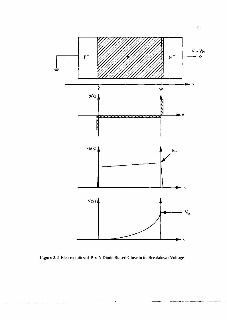
Figure 2.2 Electrostatics of P-x-N Diode Biased Close to its Breakdown Voltage

'['tic polcnri:il drop iicl-oss rt~c rcgio~i is obtained using the rel;ition
which gives
using 2.8 and assuming that the potential is zero at x = 0. Integrating 2.10 and realizing
that the breakdown voltage is V(x) evaluated at x = W gives the quadratic equation
lwhich is easily solved for W to give
Using Equations 2.12 and 2.13 and assuming a n region doping of 5x 1015cm-3 for
a breakdown voltage of 55V gives an 'intrinsic' layer width of 1.6pm.
2.3 Series and Contact Resistances
'I'he device specifications require the transorb to essentially pass zero current up
to ;III applied voltage of 50V. Beyond that the current increases rapidly while the voltage
does not exceed 60V. As seen in Section 2.2, a p-i-n diode with a breakdown voltage of
55V is chosen to implement the design. Once the diode starts avalanchiing, the junction
voltage increases only slightly, and the increasing current flow causes voltage drops in
the semiconductor bulk and across the ohmic contact resistances. It is reasonable to

a.ssume that the intrinsic layer does not contribute to the voltage drop since it is
avalanching once the breakdown voltage is reached.
To keep within the prescribed specifications, it is necessary to ke:ep the resistances
ciontributing to the voltage drops due to the avalanche current low. Specifically, if the
breakdown voltage is set at 55V, the total resistance of the diode and the contacts, Rmt,
sllould be limited to
to keep the total voltage below 60V at 150A.
As mentioned before, Rtot is comprised of two components: the semiconductor
bulk resistance and the contact resistances. The bulk resistance is given by
where p is the resistivity of the semiconductor bulk in Qcm, L is the bulk thickness, in
this case the wafer thickness, and A is the device area [I]. The resistivity of n type
gal.lium arsenide doped -1018cm-3 i s approximately 2 x 10⁻³ Rcm I I ] and a typical wafer
is around 500pm thick. The contact resitance is given by
wh'ere p, is the specific contact resistance. The specific contact resistance of p and n
con~tacts to gallium arsenide doped -1018cm-3 is, as a conservative estimate, of the order
of 1.0-4Qcrn2 131. Since the transorb consists of two back-to-back p-i-n diodes, the total
resistance is given by
whi'ch includes the two semiconductor bulks, the two n contacts and the two p contacts of
the ~transorb.
From 2.14 and 2.17

Plugging in typical values of p, p,, and L in 2.18 gives
A > 0.01 8cm2.
The diodes, therefore, need to be at least 0.018cm2 in order to meet the series resistance
specification.
2.4 Heat Dissipation During Pulse
As mentioned in Chapter 1, the transorb is to operate at 150A current pulses at a
breakdown voltage of 60V. The current pulses are to have a rise time of 6ps and a fall
time of 140ps. The total power to be dissipated through the device is, therefore, 9kW.
This dissipated power is going to appear as heat across the semiconductor resulting in semiconductor selfheating which could result in a thermal breakdown of the
semiconductor material [I]. In addition, this heating will also effect tile breakdown
voltage of the junction since the breakdown mechanism is by avalanching and the
avalanche breakdown voltage increases linearly with increasing temperature [ 1,4,5]. This
section studies the selfheating phenomenon in greater detail by examining design curves
for transient heat flow through semiconductors generated by Cooper [ti]. These curves
will be used to determine the temperature rise across the junction because of selfheating,
which will be used to predict the change in breakdown voltage. Limiting the temperature
rise to within nondestructive limits will provide the necessary design c:onstraints.
2.4.1 Transient Heat Flow in Semiconductors
Cooper has performed a numerical simulation of the transient heat flow in a
cylindrical solid of finite thickness and infinite radius, where the top s~~rface is heated by
a heating disk of finite radius and heat is removed from the bottom surface into a heat
sink of infinite radius as shown in Figure 2.3a. This geometry is typiciil of most
semiconductor device applications, including the transorb, and the curves generated can
be applied directly. Figure 2.3b shows curves which provide the transi.ent temperature
rise at the center of a circular heating disk of various radii on a substrarte of finite
thickness. This represents the greatest temperature rise in the semiconductor and is,
therefore, a worst case condition. The symbols in Figure 2.3, as applicable to the
transorb, are

_ _ _ C _ _ _ - - - - - - - - - - - - - - - - - .. - - - - - - - C
C - 8 8
I T ~ e a t i n ~ Disk \
Time (s)
I I I I Semiconductor I I I 1
\ \ \ \ \ \ \ \ \ \ \ \ \ \ \ \ \ \ \
Heat Sink
Figiure 2.3 (a) Geometry for Transient Heat Flow Simulation [6] (b) Design Curves for Transient Heat Flow Through a Semiconductor [6]. The time axis and the axis on the right are for gallium arsenide with L=500pm.
I
R=R R o R=R max
I I I I
k Z=L \\\\\\\\\\\\\4

K Themal conductivity of gallium arsenide in W/cm K T Themal 'drop' between the surface and the heat sink in K
FO Heat flux through the semiconductor in ~ / c m 2
L Semiconductor substrate thickness
b Device radius (the heating disk) in cm K Thermal diffusivity of gallium arsenide in cm2/s
t Duration of heating transient in s.
2.4.2 Transient Heat Flow in One-Dimension
The curves in Figure 2.3(b) can be easily applied to the transorb assuming one
dimensional heat flow in the z direction only (ROIL = 00). In this case,, the temperature
rise for small can be expressed as [6] L*
where Fo, the heat flux per unit area is given by
where P is the dissipated power, V the voltage across the junction, I the diode current, and
A the device area. Equation 2.20 is applicable early in the heating transient when the heat
has still not reached the heat sink Therefore, the semiconductor is still in the process of
heating up and the temperature rise grows with increasing time.
In the limit of large the heat has reached the heat sink, the temperature rise has L ~ '
reached a steady state, the heat flow curve flattens out, and the tempera.ture rise which is
now independent of time is given by
using Equation 2.2 1.
Equations 2.20 through 2.22 can be represented graphically as shown in Figure
:2.4.

time (s)
Figure 2.4 Design Curves for One-Dimensional Heat Flow. The time axis on the top and the axis on the right are for gallium arsenide with L=SOOpm.
2.4.3 Temperature Rise for Transorb Mounted Face-Up
The above curves are valid for a heating transient that occurs over a specified
period of time at a constant flux density. The heating flux in the case of the transorb is
modeled, as mentioned before, as a current pulse of rise time 6ps and fall time 140ps.
The total charge contained in a such a pulse with a peak amplitude of 150A is given by
the area under the pulse and is
This charge is equivalent to a 150A pulse applied constantly for 73ps. We can now use Equations 2.20 through 2.22 with t = 73ps. The thermal diffusivity, K, of gallium arsenide is 0.24cm2/s and the thermal conductivity, K, is 0.46W/cm K [I]. With L =

500pm for a typical gallium arsenide substrate, the x axis value in the c!wes of Figure
2.4 is
for t = 73ps. At this stage, as seen from Figurc 2.4, the heat flow has still not reached a steady state and we can use Equation 2.20. Equating 2.20 and 2.24, and limiting the
temperature rise to 100 K, we get
for the transorb size. However, process and material limitations make the design of a
(device this large prohibitive and an alternate way of effective heat dissipation which
reduces the device area significantly has to be devised.
:2.4.4 Temperature Rise for Transorb Mounted Face-Down
We see from Figure 2.4 that the area of the transorb will be reduced by operating ,at a smaller length, L which can be reduced in several ways. Possible rnethods of doing
this include etching off the back of the GaAs substrate, effectively reducing the substrate
thickness, hence the length, L. Yablonovitch et. al. have proposed a lift-off process that
selectively removes large area epitaxial films from the substrate [71. In some cases,
(GaAs substrates have been thinned by lapping the back side until the required thickness
.is achieved. Both methods require handling of extremely thin wafers. An alternate way
of achieving the same result is to mount the device face-down. This effectively brings
the active region closer to the heat sink and reduces L. In Section 2.2, we calculated the i
region to be 1.6pm thick. With L - 2pn now, Figure 2.4 shows that the temperature rise
is in steady state and Equation 2.22 can be used. Equating 2.22 to 2.24 we get
!where the maximum temperature rise has been limited to l00K as before.
The heat flow through the device is also responsible for a thermal effect which
ixppears as a resistance in the device I-V characteristics. This thermal effect can be
explained using the design curves presented above and the temperature dependence of
Ixeakdown voltage. A discussion on this is presented in Chapter 4 along with a

comparison of results from a simulation of the above effect with the exlperimentally (obtained data.
2.5 Wafer Cross Section and Mask Layout
As discussed above, the intrinsic region needs to be 1.6pm wide. The p and n
regions need to be degenerately doped to reduce bulk resistances. We use wafers of three
different cross sections. Two of the films used are grown by molecular beam epitaxy (MBE) and have i region thicknesses of 1.4 and 1.6pm respectively. The third film is grown by metallorganic chemical vapor deposition (MOCVD) with an i region thickness
a4 1 . 6 ~ . Chapter 3 presents a discussion on the differences between the two growth proecesses.
Film cross sections are shown in Figure 2.5. The 1 . 4 ~ i-layer MBE film is the
same as the 1.6pm MBE film except for the i region thicknesses.
Three mask sets are used for wafer patterning. The masks are laid out on Brutus,
a software created at Purdue, and are generated on the Cambridge Electron-Beam
Lithography or the Gyrex Pattern Generator Systems. The first mask set consists of
diodes of areas 0.08,0.04,0.02, and 0.01cm2. The second mask set consmists of diodes of
aeas 2 . 5 ~ 10-3,5x 10⁻³, and 15x10-3 cm2. It also includes a test chip with diodes of areas between 1.6~10-5 and 104 cm2 and test structures to measure contact resistances.
Dlevices on the test chip are used for most of the I-V testing presented in Chapter 4. A
la,yout of the test chip is shown in Figure 2.6. The TLM structure shows the mesa and
contact levels, the CKBR structure shows the contact level only, and all other features are
diode mesas with the contact sizes written inside. The diodes in the middlle of the die are
pl;~ced at varying distances, with the distances noted as appropriate. The third mask set
consists of diodes of areas 0.02,0.01, and 0.005cm2.

i GaAs 1.6p.m
1 GaAs Substrate
i GaAs l.6pm
GaAs Substrate
0)
Figure 2.5 Cross Sections of GaAs Films Grown by (a) MBE and (b) MOCVD

contact sizes: c l : 25x25
All measurements in pm
Figure 2.6 Layout of Test Chip

CHAPTER 3 DEVICE FABRICATION
3.1 Introduction
The transorb is fabricated using a three mask-step process. The first mask
patterns the metal contacts, the second mask defines individual devices by a mesa etch,
and the third mask isolates the devices by patterning a layer of insu1at:or. The devices
are then sawed apart and mounted face-down on a heat sink as discussed in Chapter 2. The devices are made using gallium arsenide films grown by Moleculirir Beam Epitaxy
(MBE) and Metallorganic Chemical Vapor Deposition (MOCVD). This chapter
explains the key issues in MBE and MOCVD growth and describes th'e three-mask
processing steps for the transorb.
3.2 Layer Growth
The films are grown using MBE and MOCVD. The MBE growth is done by
Professor Mike Melloch of Purdue University on his Varian Gen II MIBE system. The
MOCVD growth is done by Dr. Nasser Karam of Spire Corporation in Bedford,
Massachusetts.
3.2.1. Molecular Beam Epitaxy
The technique of growing an oriented single crystal layer on a substrate is called
epitaxial growth, or epitaxy [8]. Vapor phase epitaxy (VPE), where the crystalline layer
is grown from the vapor phase, is the most common form of epitaxy used in silicon
processing. In liquid phase epitaxy (LPE), the material to be deposited is in liquid form. During molecular beam epitaxy (MBE), the crystalline layer is formed from a thermal
beam of molecules. Both LPE and MBE are being used widely in gallium arsenide
technology [9].

In the MBE growth technique for gallium arsenide and aluminurn gallium
ausenide, gallium, arsenic molecules (As2 or Asq), aluminum, and appropriate dopant
a toms are evaporated from heated crucibles within an ultrahigh vacuum chamber I 1 0 1 . 'Ihe substrate is heated to temperatures of 550-700°C to provide sufficient energy to the
source molecules to allow them to migrate to proper low-energy bonding sites. The
n~olecular beams react at the site of the heated substrate to form layers of GaAs or
AlGaAs. Doping is achieved by exposing the substrate to a molecular beam from a
crucible containing the appropriate dopant. Mechanical shutters interrupt the beams as
needed to produce variations in doping and composition. Since the shutters can be
turned on or off rapidly, excellent abruptness of interfaces can be obtained. Growth
rates and doping concentrations are controlled by varying the temperatures of the source
crucibles. Using silicon as n-type dopant and beryllium as p-type dopant, a wide range
of doping concenaations, typically 1014 to 1019cm-3, is possible. Growth rates are
typically around lj.un/hour which corresponds to one monolayer per second. Figure 3.1
shows a representative MBE system.
High flexibility, convenience in growth of complicated structures and accuracy
make MBE popular in In-V and 11-VI semiconductor research. Principal limitations of
MBE are low throughput and high capital costs. In addition, morphologilcal defects,
known as oval deffects, in the epitaxial layer have been know to reduce device yield
[IlO].
3.22 Metallorganic Chemical Vapor Deposition
Chemical vapor deposition (CVD) deposits thin films on a substrate by thermal
decomposition and/or reaction of gaseous compounds [9]. The source ma.teria1 is
deposited directly fmm the gas phase onto the surface of the substrate. C'VD systems
include atmospheric-pressure CVD (APCVD), low-pressure CVD (LPCVD), plasma
enhanced CVD (LPCVD), and metallorganic CVD (MOCVD), also known as
org:anometallic vapor phase epitaxy (OMVPE) [lo].
MOCVD uses gaseous sources of the organic compounds of the epitaxial layers.
GaAs or AlGaAs are produced by the reaction of arsine, AsH3, with mmethyl gallium
(Ga(CH3)3) or mmethyl aluminum (Al(CH3)3) molecules present in a hydrogen gas
sw:am [lo]. (Recently, the use of solid arsenic as a source has been reported [ l 11.)

Shurtcr \ \ Electron Gun
Si Source
Ga Source
As Source
A1 Source
Be Source
RHEED screen to monitor crystal
(a)
growth
Mass flow AsH3 mntmller'\ in H2
Exhaust -
(b) Figure 3.1 Schematic Layouts of (a) MBE [12] and (b) MOCVD Grovvth Systems [lo]

The reaction takes place on a GaAs substrate heated to 650-800°C within a cold-wall chamber. The pressure within the chamber is typically 0.latrn. Typica.1 dopants are Zn in the form of diethyl zinc (Zn(C2Hjh) for the p material and silane (S:iH4) or hydrogen
:selenide (H2Se) for the n material. The compositions and dopings are controlled by
imodulating the gas flows from the various sources. High gas velocities, small gas
lnanifolds and appropriately designed chambers result in the most abrupt variations.
IMOCVD growth rates are higher than MBE rates. Typically, growth ra.tes of 5-25pm/hr
are used. A representative MOCVD system is shown in Figure 4.2.
Major advantages of MOCVD are as follows. MOCVD is suited to multiwafer gmwth 1131 and its throughput is higher than MBE, deep level donor tralps in MOCVD
IilGaAs are fewer than in the Si-doped MBE grown samples [lo], and gallium arsenide
solar cells grown by MOCVD have shown higher efficiencies than those grown by MBE
[14]. Principal disadvantages of MOCVD include the difficulty in obtaining high purity
s'ource gases, the need for extensive care in handling arsine and other gases, and the difficulty in calibration due to the considerable number of factors that effect doping and
c'ornposition, and the fact that p doping has been limited to less than ~ O l ~ c r n - ~ [lo].
3.3 Sample Preparation
3.,3.1 Cleaning Procedures
The glassware used for the processing is first cleaned. The utens:ils are soaked in
313Cl:2HN03 for five minutes followed by a 30 minute rinse in DI water and then dried
with dry nitrogen. The 2" gallium arsenide wafer is then cleaved into four quarters.
Cleaving is done by applying a gentle pressure with a razor blade at the wafer edges
pe:rpendicular and parallel to the wafer flat. The samples are then degreased in
electronic grade solvents in the following sequence: Five minutes in triclhloroethane
followed by five minutes in methonol, followed by five minutes in acetone, and finally
five minutes in methonol. A DI rinse and nitrogen dry complete the process.
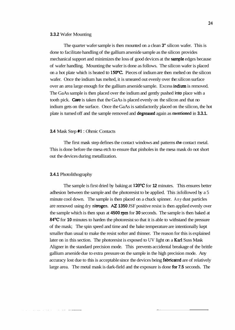
3.3.2 Wafer Mounting
The quarter wafer sample is then mounted on a clean 3" silicon wafer. This is
done to facilitate handling of the gallium arsenide sample as the silicon provides
mechanical support and minimizes the loss of good devices at the sarnple edges because
of wafer handling. Mounting the wafer is done as follows. The silicon wafer is placed
on a hot plate which is heated to 150°C. Pieces of indium are then melted on the silicon
wafer. Once the indium has melted, it is smeared out evenly over the: silicon surface
over an area large enough for the gallium arsenide sample. Excess indium is removed.
The GaAs sample is then placed over the indium and gently pushed into place with a
tooth pick. Care is taken that the GaAs is placed evenly on the silicon and that no
indium gets on the surface. Once the GaAs is satisfactorily placed on the silicon, the hot
plate is turned off and the sample removed and degreased again as mczntioned in 3.3.1.
3.4 Mask Step #1 : Ohmic Contacts
The first mask step defines the contact windows and patterns the contact metal.
This is done before the mesa etch to ensure that pinholes in the mesa mask do not short
out the devices during metallization.
3.4.1 Photolithography
The sample is first dried by baking at 120°C for 12 minutes. This ensures better
adhesion between the sample and the photoresist to be applied. This :is followed by a 5
minute cool down. The sample is then placed on a chuck spinner. Any dust particles
are removed using dry nimgen. AZ 1350 JSF positive resist is then applied evenly over
the sample which is then spun at 4500 rpm for 30 seconds. The sample is then baked at
84OC for 10 minutes to harden the photoresist so that it is able to withstand the pressure
of the mask; The spin speed and time and the bake temperature are intentionally kept
smaller than usual to make the resist softer and thinner. The reason for this is explained
later on in this section. The photoresist is exposed to UV light on a K.arl Suss Mask
Aligner in the standard precision mode. This prevents accidental breakage of the brittle gallium arsenide due to extra pressure on the sample in the high precision mode. Any
accuracy lost due to this is acceptable since the devices being fabricatred are of relatively
large area. The metal mask is dark-field and the exposure is done for 7.5 seconds. The

isample is then soaked in chlorobenzene for 17 minutes. This soak removes residual
:solvent and low-molecular weight resin from the surface, creating a derrse surface layer
1.ess susceptible to resist developer [15, 16, 171. When the resist is developed, the resist
underneath the dense surface layer develops faster leaving an undercut in the resist as
shown in Figure 3.2. This undercut in the developed resist is desirable Ikcause it assists
the liftoff procedure to be discussed later. Following the chlorobenzene soak, the
s,ample is dried with dry nitrogen and the resist is developed out in a 1 P~Z351 developer
: 5DI solution. Following developing, the sample is rinsed in DI water and dried tigain
using dry nitrogen.
3.4.2 Metallization
A two layer contact of TiAu is evaporated in the Varian e-Beam Evaporator at
Purdue. Since gold is very soft and gallium from the GaAs is believed to out-diffuse in
to the gold [18, 19,201, the titanium layer is evaporated as a barrier layer which
pirovides mechanical support, prevents the metal getting removed due to probing and
re:stricts gallium out-diffusion. Native oxides from the surface of the gallium arsenide
are first etched in an NHqOH:40DI solution for 60 seconds. Following a. DI rinse and
nitrogen dry, the sample is place immediately in the metallization chamber for pump
down. The thickness of the deposited metal can be closely monitored on the Varian
evaporator using a crystal monitor. A lO0OA layer of titanium is evaporated followed
by a 2000A layer of gold. The evaporation is performed at a pressure of -5-8 x
to.rr.
3.44.3 Lift-off
Once the metal is evaporated, the sample is rea.d j. for lift-off. For lift-off, the
sample is placed in a pem dish and acetone is squirted on to it from a squeeze bottle.
The acetone attacks the resist underneath the metal and the metal is lifted off leaving
contacts on the surface. Following the lift-off, the sample is degreased, rinsed in DI, and
dried with nitrogen.

Figure 3.2 Mask 1 Processing Steps (a) Developed positive photoresist follc~wing chlorobenzene soak. (b) Following metal deposition. Note the discontinuity in the metal due to ridge in the resist profile. This ailds the liftoff process as discussed in the text. (c) Metal contact following liftoff.

+ N substrate
Metal T i A u
Contact
(c)
Figure 3.2

3.5 Mask Step #2 : Mesa Etch
The mesa mask defines the individual diodes and is a light-fielld mask.
3.5.1 Photolithography
The sample is first hard baked as before at 120°C for 10 minutes followed by a 5
minute cool-down period. A Z 1350 JSF positive resist is then spun 011 at 4500 rpm for
40 seconds. The sample is soft baked for 10 minutes at 90°C. Wafer-to-mask alignment
and resist exposure to UV light are done on a Karl Suss Mask Aligner in the standard
precision mode. The exposure time is 6.5 seconds. Following exposure the resist is
developed out in a 1AZ351 : 5DI solution. Following a DI rinse and nitrogen dry, the
sample is hardbaked for 20 minutes at 120°C to harden the resist for the mesa etch processing.
3.5.2 Mesa Etch
Two different types of mesa etch solutions are used. The basic: difference
between the two etches is the etch rate. The first etch uses a 3H3P04:'lH2@:5ODI
solution and results in an etch speed of 1000A1minute. The second usczs a
lONH40H:3.5H2@:500DI solution and gives an etch rate of 2000 h n u t e . The etch
is done while holding the sample in a beaker filled with the etch solution being stirred
with a magnetic stirrer at 100 rpm. The mesas are etched for 2.25 pm. This ensures that
the etch is well into the n+ region of the film. A 2.25 pm etch is done in approximately
22 minutes for the phosphoric acid etch and 11 minutes for the
ammonium hydroxide etch. The etch is monitored by looking at the s.ample profile on a
Tencor Alpha-Step profilometer after every 5 minutes of etching. The etch is terminated
with a rinse in DI water followed by a nitrogen-dry. When the desired etch is achieved,
the resist is stripped off using two 30 second rinses in acetone. After a rinse in DI and a
nitrogen-dry, the sample is taken for yield measurements and initial pulse testing as
discussed in Chapters 2 and 4. The processing sequence is shown in F:igure 3.3.
Scanning electron microscope (SEM) photographs of the profiles of the two etches are shown in Figure 3.4. The profile of the ammonium hydroxide etch in the direction
perpendicular to the one shown is the same as that of the phosphoric ac:id etch which has
the same profile in both directions.

Figure 3.:3 Mask 2 Recessing Steps (a) Developed positive photoresist. (b) Following mesa etch. (c) Mesa isolated p-i-n diode following resist removal.

Positive Photoresist
Mesa-Isolated P-i-N diode
Figure 3.3

Figure 3.4 SEM Photographs of (a) Ammonium Hydroxide and (b) Phosphoric Acid Etches

3.6 Mask Step #3 : Device Insulation
DuPont Pyralin 2555 Polyimide (PI) is used for device insulation [21,22]. A
nimde layer could also be used but PI is preferred because of the ease in application.
The PI application procedure is adapted from references 23 and 24. The wafer is
first degreased in electronic grade solvents as before. The sample is then hardbaked for
20 minutes at 120°C to remove absorbed water. When the sample ha:; returned to room
temperature, PI is spun on at 6000 rprn for 40 seconds. The PI is then hardbaked in two
steps. A 15 minute 85OC soft-bake is followed by a 20 minute 120°C hard-bake.
Following baking, the sample is allowed to cool for 20 minutes. AZ 11350 JSF positive
resist is then spun on at 5000 rpm for 40 secs. The resist is soft-baked for 15 minutes at
85OC. The dark-field metal mask is aligned to the wafer on the Karl Sluss Aligner and the resist exposed to UV light for 7.5 seconds. Following exposure, the photoresist is
developed out and the PI etched in a single process using AZ35 1 developer with DI
water in a 1:4 solution. Once the photoresist has developed, the PI takes approximately
20 seconds to etch. The etch is halted with a 60 second rinse in DI water. After
inspecting the wafer under an optical microscope, the resist is removed with an acetone
dip. Extended contact with acetone degrades the PI, therefore a minimum rinse is used
to remove the photoresist. The sample is then DI-rinsed and nitrogen-dried. The PI is
then cured in a Lindbergh Furnace at 230°C for 20 minutes. An alpha-step profile shows
that this results in a 1 micron thick layer of polyimide. Figure 3.5 shows the processing
sequence.
3.7 Device Packaging
The wafer is then sawed apart on a Ternpress Model 602 Saw. Before sawing,
AZ 1350 JSF positive photoresist is spun on the wafer at 400 rprn for ,40 seconds and the
resist is soft baked at 75OC for 15 minutes. The photoresist protects the devices from
damage during the sawing. The devices are sawed such that the saw cuts completely
through the GaAs and partially through the silicon. Following sawing, the resist is
smpped in acetone and the wafer rinsed and dried, after which it is placed on a hot plate
and heated to 150°C. Once the indium begins to soften, it is possible to remove individual die from the sample.

Figure 3.5 Mask 3 Processing Steps (a) Polyimide spun on device. (b) Positive photoresist is added on top of the polyimide. (c) Completed p-i-n tiiode after the resist and polyimide are developed in a single step and the unexposed resist is srtipped off.

Pol yimide
Positive Photoresist
Final Diode
Figure 3.5

'The devices are next mounted on a dual inline package (DIP). Silver paste or indium is
smeared onto the package. The material is smoothed out completely and any excess is iernoved. Before the diodes are mounted, their edges must also be insulated. This is (one to prevent any shorting of the device due to metal creeping up the walls during mounting. The edges are insulated by painting PI using a paint brush. Care is taken to
e:nsure that the edges are fully covered with PI. The devices are then mounted face clown on the metal. Care is taken to prevent any metal from creeping up along the wul.ls
of the die since this would effectively short out the diodes. Once the devices have been
mounted, contact to the back n side is made by soldering a thin wire to the indium on
tlhe back of the wafer. The wire is soldered and not bonded because bonding to indium
is not possible. The final device is shown in Figure 3.6.

v Soldered Wire
Figure 3.6 The Completed Transorb

CHAPTER 4 EXPERIMENTAL RESULTS
4.1 Introduction
The transorb characterization is carried out in the solid state characterization labs
at Purdue University. This chapter presents the results obtained. Section 4.2 presents the
I- V characteristics obtained for the transorb and examines the breakdown voltage in
greater detail. The experimentally obtained values of the series and contact resistances
are also presented. The heat flow resistance of the transorb and the temperature de:pendence of the breakdown voltage are discussed in Section 4.3. Section 4.4 co~ncludes with failure results and a discussion on failure mechanisms.
4.2 I-V Characteristics of Transorb
The I-V measurements are done on a Hewlett Packard 4145 Semiconductor
Paramater Analyzer. The devices are probed in a Micromanipulator probe station.
Typical results are shown in Figure 4.1 for the MBE wafer. We measure two types of
characteristics for the MOCVD sample. Figure 4.2 shows one of these while the other is
given in Section 4.4. The following observations are significant. 1. The breakdown voltage is lower than the designed voltage. 2. The effective resistance of the
chixacteristics in the avalanche regime is much larger than the expected rt:sistance. 3.
Some MOCVD diodes have a 'soft' breakdown characteristic (see Section 4.4). This
section deals with issues 1 and 2, while 3 is dealt with in a later section.
4.2.. 1 Breakdown Voltage
The breakdown voltage of both MBE and MOCVD samples ranges between 38
and 45V as shown in Figure 4.1. Table 4.1 summarizes the results.

.c'
****** GRAPHICS PLOT ******
Figure 4.1 I-V Characteristics of MBE Diode
:I F b A ) CURSOR (-43. SOOV , -950. SuA , )
10.00,
2.000' /div
0
-10.00- -50.00
-950. SuA . )
h
I I 1 I -
, MARKER (-43. SOOV ,
,
I
VF 10.00/div C V> 0 50.00
.I
. ,
- 1
LINE 1 LINE2
4e
I I m I
GRAD 3.7BE-03
l/GRAD 264E+00 -43.2E+00

****** GRAPHICS PLOT ******
Figure 4.2 I-V Characteristics of MOCVD Diode
IF CmA) CURSOR C-38.500V . -9 15.3uA , >
. 0000,
1.000- /div
-- 1 0. 00 -50.00 OOOC
MARKER
m
- m
.
- - m
.. 1 1
VF 5.000/di v C V:)
C-38.500V , -91 5.3uA , )-
4 b -
I 1 1 I I I I . Ylntorco~ 213E-03
I
LINE1 L I NE2
GRAD 5.56E-03
l/GRAD 180E+00
Xlntorcept -38.3E+00

Table 4.1 Comaprison of Breakdown Voltage for Samples with 1.4 and 1.6pm Intrinsic Region Widths. The numbers given for breakdown voltage are averages.
The diodes were designed for a 55V breakdown voltage. The design results were obtained
using a breakdown electric field of 4xl05~fcm for gallium arsenide and assuming a n region doping of 1015cm-3. The data in Table 4.1 shows that the maxilrnum electric field
in our samples is around 2.8x10⁵~fcm assuming zero doping in the intrinsic layer. Also,
the effective electric fields are lower for the longer intrinsic regions. We are unable to
present any conclusive explanation for this. However, using the measured peak field
instead of 4xlOSVfcm as before, we calculate an intrinsic region width of 2 pm to achieve
a breakdown voltage of 55V. We present a possible reason for the lower breakdown
,voltage in 4.4.2.
4.2.2 Series and Contact Resistances
Maximum Electric
Field (Vjcm)
3.2 x 10⁵
2.4 x 10⁵
3.1 x 1@
2.5 x 10⁵
2.8 x 10⁵
Process Run #
1
2
3
4
5
Figures 4.1 and 4.2 show that each diode of the transorb has an effective series I-esistance of up to 280Q in the avalanche breakdown region. The designed series
resistance was 33mQ. Tests on contact resistance measurement and series resistance measurement are conducted. Additional experiments are conducted to determine the
rource of the large resistance. These experiments reveal that this resistance is not really a
Breakdown
Voltage (V)
45
39
43
40
45
Film Growth
MBE
MBE
MBE
MOCVD
MOCVD
Intrinsic Region
Width (pm)
1.4
1.6
1.4
1.6
1.6

resistance but is a consequence of device self-heating which appears as an effective
resistance.
4.2.2.1 Contact Resistance
The contact resistance is measured using the Transfer Length Method [31. The test
structure is shown in Figure 4.3. The method works as follows. The re:sistance betwecn
successive contact pads placed at increasing distances is measured. The: measured
resistance is given by
where Rs is the semiconductor bulk resistance and IQ is the contact resistance.
Substituting for Rs and IQ in 4.1, we get
where p, is the semiconductor bulk sheet resistance, pc the specific contact resistance, d
the distance between contacts, z the width of the contact, and Ac the area of the contact.
Measured values of RT are plotted versus contact spacing d. From Equation 4.2,
the slope of the line gives the bulk sheet resistance and the y intercept the specific contact
resistance.
Figure 4.4 shows the results obtained for the MBE samples.
The y intercept is
where Ac = Lz where L, the length of the contact, is 90pm and z is 50prrr. Using these
values of L and z in 4.3 gives

Contact Pad Wpm x 50pn1
d = 5 + 10n
Figure 4.3 TLM Test Structure
0 0 10 20 30 40 50
Contact Spacing (p)
Figure 4.4 TLM Measurrnent for Contact Resistance of MBE Sample. The data fits to R~=10.912+2.25444 where RT, the total resistance, is plotted along the y axis and d, the spacing between contacts, is plotted along the x axis.

The specific resistance of the p layer is obtained using the slope. The
semiconductor resistance is given by
where t is the thickness of the semiconductor layer. Using R/d = 2.2544Wpm from Figure
4.4, z = 90pm, and t = 1500A, the thickness of the p layer, we get
for the semiconductor p layer. Using standard tables [I.] this resistivity c:orresponds to a p
layer doping of 4x1019cm-3 which agrees closely with the 5x1019cm-3 p layer doping of
our MBE grown film.
Figure 4.5 shows the TLM result for the MOCVD film. Proceeding as before, we
obtain a specific contact resistance of 1.42~10-3 Rcm2 and a p layer doping of
1.1x1019cm-3.
50 0 10 20 30 40 50
Contact Spacing (pm)
Fi,gure 4.5 TLM Measurment for Contact Resistance of MOCVD Sample. The data fits to R~=63.361+5.4398d where RT, the total resistance, is plotted along the y axis and d, the spacing between contacts, is plotted along the x axis.

4.2.2.2 Series Resistance
A simple experiment is devised to make a crude measurement of resistances other
than the top contact resistance. The total series resistance of the diode may be expressed
as &=R,+R, (4.7)
where Rt is the resistance of the top contact, and Rs is the resistance due to the
semiconductor bulk and the back contact. Equation 4.7 may be written as
?where p, is the top contact specific resistance, At the area of the top contact, p, an
effective resistivity for the semiconductor bulk and back contact together, and As is the
tievice area.
The reverse characterisitics of p-i-n diodes of different areas but same top contact
sizes is plotted on an HP 4145 parameter analyzer. The effective resistance in the post-
I~reakdown regime of each diode is measured as the reciprocal of the slope of the I-V
curve. Then, using 4.8, plotting the measured resistance versus the reciprocal of diode
ruea gives the specific contact resistance as the y intercept and the slope gives the effective
resistivity of the bulk and back contact. This gives a rough estimate of the resistances due
to the bulk and back contact and provides a check on the specific contact resistance
measured using the TLM method. Figure 4.6 shows the results for the IVIBE sample.
The y intercept of the plot, 137.368, is the top contact resistance:. The devices
measured in this experiment have a contact area of 6.84~10-6 cm2. Therefore, the specific
contact resistance is 9.4~10-4Qcm2 which is almost four times larger than the value in
Eguation 4.4 which was measured from the TLM method. The slope of the plot gives an
effective resistivity for the bulk and the back contacts and is 5.16mSZcm2.
As discussed in Chapter 2, our design aims for devices of area 0.04cm2. Using a specific contact resistance of 0.246&m2 from Equation 4.4 and an effective bulk
n:sistivity of 5.16mRcm2 from above, we see that the total series resistance in the full size
d'evice would be approximately

150 0 15000 30000 45000 60000
l/(Mesa Area) (cni2)
Figure 4.6 Series Resistance Measurement. The data fits to R T = ~ 37.36+0.005 16A,-1 where RT, the measured resistance is plotted along the y axis and A,-1, the reciprocal of the mesa area, is plotted along the x axis.
Our design aims for a series resistance of 33mR and the projection in Equation 4.9 is four times larger than our goal.
Where is the extra resistance coming from? Our design used an estimated value of
the contact resistance equal to 10-~Rcm2. TLM measurements are two-and-a-half times
larger than this assumption. Our initial calculations assumed a resistivity of 2xl0-~!2cm for
oix semiconductor bulk and a bulk thickness of 500pm. We can compare the result from th~e above experiment to our initial assumption by dividing our experimental resistivity in
Qtcm2 by the length of the bulk. Doing this gives a resistivity of 103.2~10-3Rcm which is
approximately 50 times larger than our design value.
Further investigation of the series resistance problem reveals that the larger than
expected resistivity that we measure is not a resistance at all. It is, in fact, a thermal effect
which appears as a series resistance. As we see in the next section, the design curves
presented in Chapter 2 along with the temperature dependence of the breakdown voltage
cam be used to explain this resistance.

4.3 The 'Heat How Resistance'
A series of pulsed measurements on our devices coupled with computer
simulations reveal that the large series resistances measured in our samples are not
resistances at all. They are, in fact, a thermal effect which manifests itself as a resistance.
Before this thermal effect is explained, it is neccessary to investigate tl~e temperature
dependence of the breakdown voltage.
4.3.1 Temperature Dependence of Breakdown Voltage
Figure 4.7 shows the experimental dependence of breakdown voltage on temperature for the MBE sample. Data for the MOCVD sample is presented in Section
4.4. The data is obtained with the device placed on a heated chuck on ii Micromanipulator
probe station and the breakdown voltage measured on an HP 4145 semiconductor
parameter analyzer.
310 330 350 370 390 410 430 450 470 Temperature (K)
Figure 4.7 Temperature Dependence of Breakdown Voltage for MBE Sample. The data fits to Vh = 43.3 1 + 0.034643T. where Vb is the breakdown voltage and T the absolute temperature.

Figure 4.7 shows that the breakdown voltage increases by 3.46V for every 100°C
rise in temperature. The increase of breakdown voltage with temperature is typical of
avalanche breakdown. The breakdown voltage due to Zener breakdown, which occurs because of tunneling across the bandgap, decreases with temperature because the bandgap
energy decreases with temperature [I]. In fact, such measurements are i~sed to determine
the breakdown process.
The increase of breakdown voltage with temperature for avalanclhe breakdown is
e:rcplained as follows. Avalanche breakdown occurs when charge carriers, accelerated by
the electric field, gain enough energy to impact-ionize lattice atoms creating more
ellectron-hole pairs. These secondary carriers are also accelerated to higher energies,
creating more electron-hole pairs. The process continues leading to avalanche
rr~ultiplication and breakdown [I]. As the temperature increases, the mean free path
between scattering events decreases. Greater applied voltages are therecore required to
accelerate the carriers to the energy required for impact ionization [4,5].
4..3.2 Explanation of the 'Heat Flow Resistance'
As the diode reaches its breakdown voltage, impact ionization occurs, leading to
avalanche multiplication and breakdown. The breakdown process significantly increases
th~e current through the device. As the current increases, the VI product for the device
increases. This increased flux results in a temperature rise in the junction which increases
th~e breakdown voltage further. Figure 4.8 shows this effect . At A, the heat flux causes a
temperature rise which increases the breakdown voltage to B. As the process repeats
itself, the I-V characteristics trace out line segment AD. Note the difference in the slopes
of the line without any heat flow and the line segment AD.
The heating effect shown in Figure 4.8 can be simulated using the heat flow curves
presented in Chapter 2 and the temperature dependence of the breakdow~~ voltage
investigated in Section 4.3.1. Specifically, we use Figure 2.4 and Equatilons 2.20 and 2.22
alongwith avbr - = 35mVPC aT
(4.10)
as, determined in Section 4.3.1. Note that the design curves in Figure 2.4 predict that the
temperature rise increases as the square root of time (Equation 2.20). However, we see in
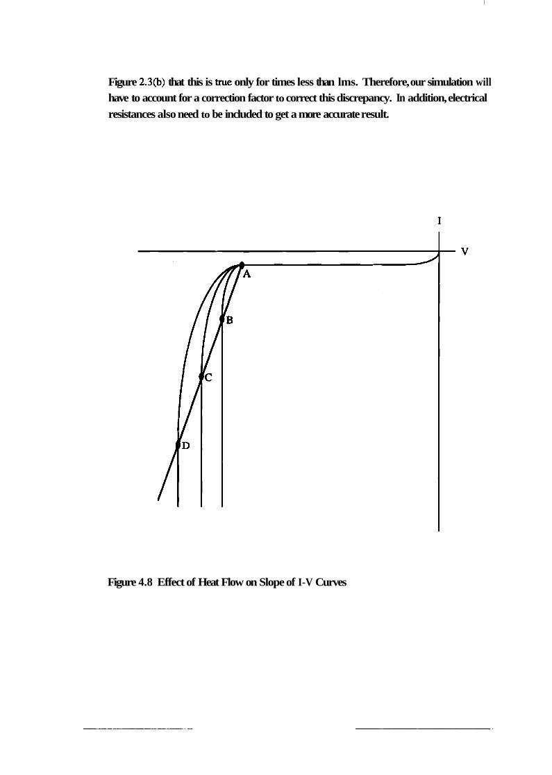
Figure 2.3(b) that this is true only for times less than lms. Therefore, our simulation will have to account for a correction factor to correct this discrepancy. In addition, electrical resistances also need to be included to get a more accurate result.
Figure 4.8 Effect of Heat Flow on Slope of I-V Curves

4.3.3 'Heat Flow Resistance' Simulation Results
A computer program is written in the 'C' programming language to perform the
above simulation. The program listing is given in the appendices. The program is run for
one of our MOCVD samples. We assume a gallium arsenide substrate with a length of
500pm, a device size of 104cm2, and the simulation is run for 5, 10,20,30,40,50,60,
and 75ps pulses. Assuming a circular diode, a device size of 104cm2 corresponds to a
rildius of 56.4pm, giving RO/L = 0.1 13. The program starts with a breakdown voltage of
38.8 volts and assumes an initial cunent flow of 1 . W for each case. Figure 2.4 shows
that we can use Equation 2.20 for all eight pulses. The program uses Equation 2.20 to
ciilculate a temperature rise which translates into an incrtase in breakdown voltage using
Equation 4.10. The current is incremented by 1rnA and the new VI product is used to calculate the next temperature rise. The program repeats till a current of 50mA is reached.
The correction factors mentioned above are determined as follows. The exact vidue of t h e n factor is determined for each pulse width from Figure 2.3(b) which is
FoL redrawn in Figure 4.9 zooming in to the area of interest. The equivalent simulation result
obtained using Equation 2.20 is divided by this value to give the correcti~on factor. Table
4.2 gives the results.
Time (s) loJ lo"
0.5 0.2 -2
R oJL 10
Figure 4.9 Design Curves to Determine Exact Value of= The time axis and the axis F,L'
on the right are for gallium arsenide with ld=5fi0prn.

Table 4.2 Calculation of Correction Factors for Heat Flow Simulation Results
-KT (simulation) FnL
Correction Factor

We now calculate the electrical resistances to be added to the co~~ected results.
VVe assume a p contact size of 95pm x 95pm. From above, the TLM result for the specific contact resistance for the MOCVD sample is 1.42 x 10⁻³Rcm2. In addition, we assume an n contact resistivity of 104Qcm2 and an n contact of 104crn2!. The p and n
contact resistances then are
respectively.
The bulk resistances are calculated using resistivities determined from standard
tables [I] and the known dimensions. The results are
and
where Rp+ and R,,+ are the resistances of the p+ and n+ semiconductor bulks respectively.
The resistivity values in Equations 4.13 and 4.14 correspond to an acceptor doping of
7..'jx1018 cm-3 and a donor doping of 1.5~1018 cm-3 respectively. The total electrical
resistance is, from Equations 4.1 1 thru 4.14,
Our program includes the correction factors in Table 4.2 and the resistance in
Equation 4.15 in the simulation. The final results are presented in Figure: 4.10.

0 38 39 40 41 42 43
Reverse Voltage (V)
38 39 40 41 42 4.3
Reverse Voltage (V)
Figure 4.10 'Heat Flow Resistance' Simulation Results (a) 5, 10,20 and 30 ps pulses. (b) 40,50,60, and 75 ps pulses

4..3.4 'Heat Flow Resistance' Experimental Results
The experimental set up used for this experiment is shown i n Figure 4.1 1.
Figure 4.11 Experimental Set-Up for 'Heat Flow Resistance' Measuremtmt
An HP 214A Pulse Generator operated i n trigger mode is used to generate pulses
of width 5, 10.20, 30, 40, 50,60, and 75ps. The experimental procedun: is as follows.
The pulse generator is set at 5V and Sps pulse width in the trigger mode. The pulse is
triggered and the input pulse, the pulse across the current limiting resistor, and the reverse-
biased diode are viewed on a Tektronix 11401 Digitizing Oscilloscope. The voltage across
th~e diode and the resistor give one data point for the reverse biased I-V characteristic. The
supply voltage is increased and the next data point recorded. Once the I-V characteristic
hits been traced out, the pulse width is set to lops and the procedure repekated. The I-V
characteristic for the other pulse widths are obtained similarly. Figure 4.12 gives the
experimental results. Figure 4.13 compares the experimental and simulation data by
plotting effective resistance versus pulse width.

Reverse Voltage (V)
(a)
38 39 40 41 42 43
Reverse Voltage (V)
Figure 4.12 'Heat Flow Resistance' Experimental Results (a) 5, 10,20 and 30 ps pulses. (b) 40,50,60, and 75 ps pu1:ses

Pulse Width (ps)
Figure 4.13 Comparison of Experimental Results with Simulation Results. The solid line is the simulation result and the points are the experimental data.

Figure 4.13 shows that the simulation results using the design curves, the
experimental dependence of breakdown voltage and the measured and ap:proximated
re:;istances are in close agreement with the experimental data. We are therefore in a
position to extend the above simulation to the full-size device operating at the required
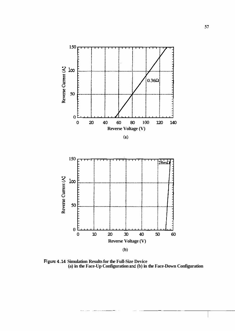
current levels. Assuming a p contact resistivity of 1flQcm2 and the n contact and the p
and n bulk resistances as before, RT in Equation 4.15 is now given by
for a full-size device of area 0.04cm2. The correction factor for the 73ps pulse width in
the specifications is found to be 1.398. Figure 4.14 (a) shows the result for a full-size
device operating in the face-up configuration. We see that the full-size device is off by a
factor of 10 when mounted face-up.
The above discussion is extended to the device operating in the face-down calnfiguration as follows. The length, L, is now the intrinsic layer thickness plus the p+
1a:yer thickness and is 1.9pm. We see from Figure 2.4 that the heat flow lnas reached
steady-state in this case and the temperature rise is given by 2.22. The silmulation results
are given in Figure 4.14 (b) for a full-size device operating in the face-down configuration.
Wt note from 4.14 (b) that the full-size device operating in the face-down configuration
easily meets the prescribed specifications. Note also that the simulation ~~esults of Figure
4.14 (b) overestimate the 'heat flow resistance' as evident from a comparison of Figures
2.3 (b) and 2.4 at 7 3 ~ s . Incorporating an appropriate correction factor would further lower
the slope in 4.14 (b). Since we have already established that the design specifications
limiting the series resistance are met, we omit this correction.
Now that we have established by simulations, which have been piutly verified by
experimental results, that the device mounted face-down successfully meets the
specifications, we proceed with operating the device at the current densities it was
designed for. Specifically, the pulse-bias experiment, described earlier in this section, is
continued at a fixed pulse width until the device fails. Experimental results so obtained
are presented in the next section. We also present a comparison of the MIBE and MOCVD devices and suggest an explanation for device failure in both cases.
n
3 loo
0 20 40 60 80 100 120 140 Reverse Voltage (V)
n
loo
0 10 20 30 40 50 60
Reverse Voltage (V)
Figure 4.14 Simulation Results for the Full-Size Device (a) in the Face-Up Configuration and (b) in the Face-Down Configuration

4.4 Device Failure
As mentioned above, the pulse experiment described in the previous section is
continued at a fixed pulse width until the device under test fails. We calculated in
Chapter 2 that the required area for a full-size device mounted fdce-up is 0.924 cm2. A
peak current of 150 A therefore represents an equivalent current density., J, of 162 Afcm2.
The results obtained are presented below.
Both MBE and MOCVD diodes are tested to destruction. Our experiments reveal
that both MOCVD and MBE diodes of area less than lo4 cm2 fail as a result of thermal
instability leading to device burnout. In some cases the damage is visible as a burnt
portion on the device when viewed under an optical microscope. In the discussion that
fiollows, we use the design curves presented in Chapter 2 to calculate tht: maximum
temperature rise at bum-out. Testing on MBE diodes larger than 0.01 cm2 reveals that
no large device works. We attribute this to oval defects present in MBE grown wafers.
PIlOCVD diodes of area larger than 0.01 cm2 are also tested. We find that these devices
f i d at a current density two orders of magnitude smaller than the smaller devices. We
believe that microplasma formation is the failure mechanism in this case:.
4.4.1 Failure of MBE-Grown Diodes
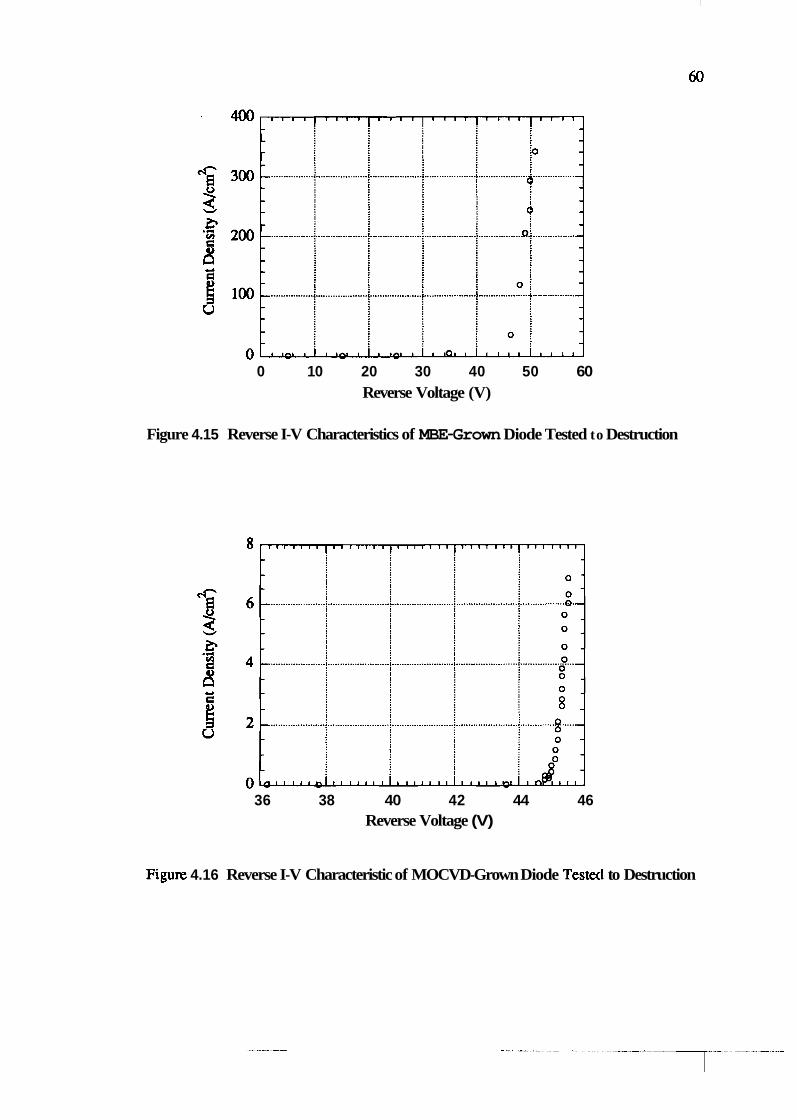
Figure 4.15 shows the I-V characteristics obtained for a lOOxlOO pm diode tested
tch destruction using the pulse measurement described earlier. The devicle is tested at a
pulse width of 75 ps. The device fails at a peak current density of 341 A J C ~ ~ . This is a
factor of two higher than required by our design specifications for a device mounted face-
up. We use the design curves presented in Chapter 2 to predict the temperature rise that this current density represents. We found the exact value of the y axis quantity, in
F,L'
Figure 2.3 (b) for a 75 ps pulse in Table 4.2 to be
w'hich gives

as the temperature rise in the semiconductor. Assuming a heat sink temperature of 23"C,
this represents a junction temperature of 15 1 O C .
The device failure mechanism is as follows. The heat dissipatiorl caused by high
reverse current densities at high reverse voltage increases the junction temperature as
cidculated above. This temperature rise increases the breakdown voltage and decreases
the current. Because of this effect, the I-V characteristic shows a negative differential
rr:sistance [I]. The current density, even in carefully manufactured junctions not
containing localized breakdown regions, is a function of position [25]. If there is a slight
unbalance of current density in the negative resistance region, the current will be
concentrated at one point because the current-concentrated region needs less voltage 1261.
This current concentration effect and the jump to lower voltages, known as second
bl-eakdown 126, 27,281, causes excessive temperature rise leading to device destruction
due to bum out [I, 25,261.
As mentioned above we are unable to obtain any MBE devices of' area larger than
0.01 cm2 that work. We attribute this to oval defects in the epitaxially grown layer.
MIelloch et. al. [14] have determined in a study conducted at Purdue that the oval defect
density of an MBE grown sample at Purdue is 500/cm2. Using the standlard yield
quation [9]
wlhere A is the device area and Do the defect density we get
Y = 0.7%
for a defect density of 500Icm2 and a device area of 0.01 cm2.
4.4.2 Failure of MOCVD-Grown Diodes
The I-V characteristics of the MOCVD-grown diodes of area less than ~ O - ~ c m ~
arc: similar to the ones obtained from MBE-grown diodes. We conclude t:hat the failure
mechanism in this case is also due to device heating. The I-V characteristic of a 0.02cm2
device tested at a pulse width of 20ps are shown in Figure 4.16.
0 10 20 30 40 50 60 Reverse Voltage (V)
Figure 4.15 Reverse I-V Characteristics of MBE-Grown Diode Tested to Destruction
36 38 40 42 44 46 Reverse Voltage (V)
Fi,gure 4.16 Reverse I-V Characteristic of MOCVD-Grown Diode Testecl to Destruction

We see that the device fails at a current density of less than 7 A/c:m2. We see fivm Figure 4.3 (b) that the temperature rise for a pulse width of 20ps for R& = 1.6 has
not reached steady state and that we can apply Equation 2.20 directly. A.lso note that a
correction factor is not needed. Equation 2.20 gives
for a 20 ps pulse, which is a temperature rise of less than 2°C. The fai1u:re mechanism is,
therefore, not due to device-heating. We suggest that the failure mechanism in this case
is microplasma formation.
Structural defects in the semiconductor material increase electric fields and act as
sites for premature avalanche breakdown. These localized breakdown regions, called
rn~icroplasmas, have been found in avalanching p-n junction devices [29-,401. We
attribute the failure of our diodes to microplasmas because of the following reasons. F~~rst, our devices showed lower breakdown voltages. As mentioned above,
microplasmas lead to premature avalanche breakdown, resulting in lowel- breakdown
voltages. Therefore samples with microplasmas have breakdown voltagt:~ lower than
those without microplasmas [29,32,33,39]. Second, some of our MOCVD devices
show a 'soft' breakdown characteristic as shown in Figure 4.17. Logan et. al. and La1 et.
al. [30, 311 report that 'soft' breakdown and microplasmas are concomitant. Figure 4.18
sh~ows the temperature dependence of breakdown voltage for our MOCVD sample. Note
the two distinct regions of breakdown voltage dependence. Similar results obtained by
Bishop [39] have been attributed to microplasmas. Finally, Ghandhi reports successively
lower breakdown voltages for samples containing microplasmas [40]. Oiur samples
showed similar results.
We are unable to present a conclusive explanation for the existence of
microplasmas in the MOCVD samples. Even though oval defects in the :MBE material
make the design of the transorb prohibitive, our experimental results have established that
a scaled-down version of the transorb is realizable. An attempt at meeting the
specifications is possible by connecting several working small size devices in an array of
diodes in parallel equivalent in area to the full-size device. However, such a design
would be difficult to implement considering the required area for the transorb (0.04 cm2)
and the largest size diode (lo4 cm*) that we successfully tested. Specifically, we would

Figure 4.17 'Soft' Breakdown Characteristics for MOCVD Sample
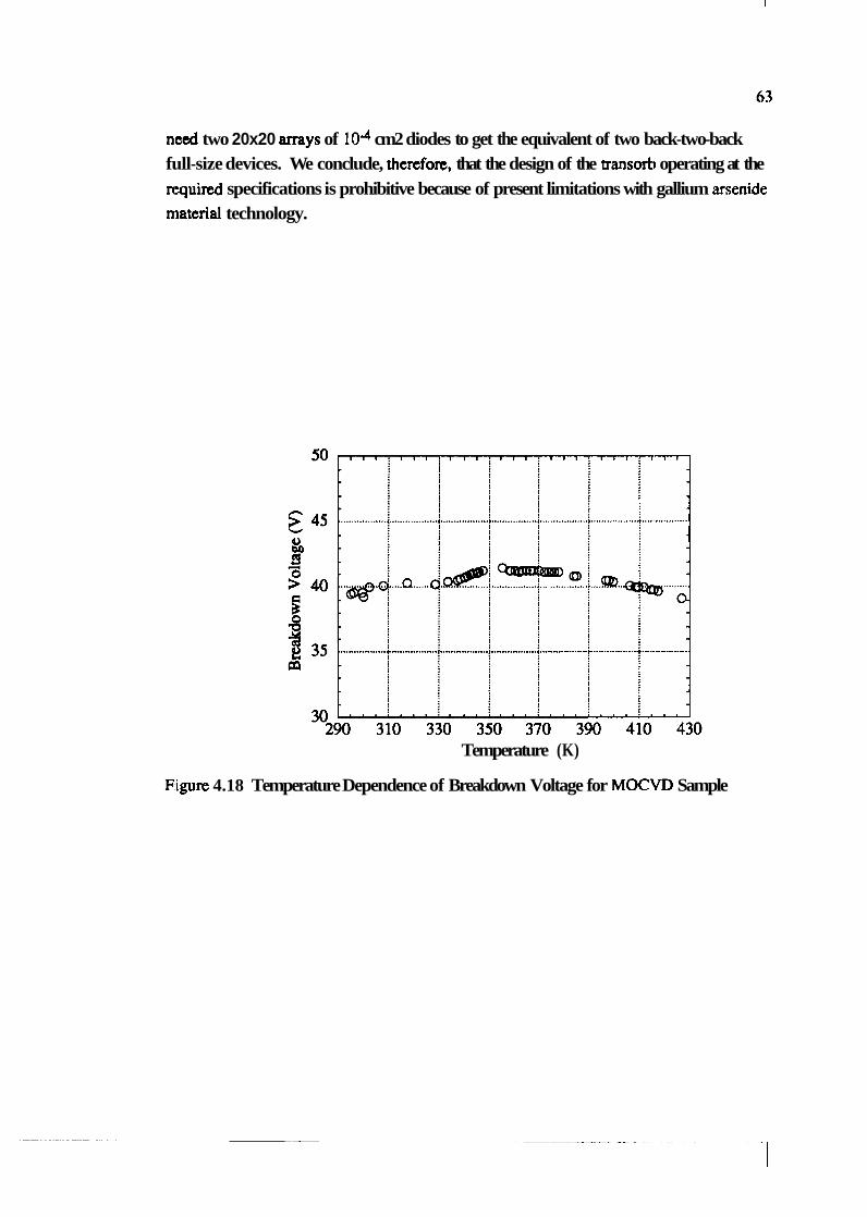
need two 20x20 arrays of 104 cm2 diodes to get the equivalent of two back-two-back full-size devices. We conclude, therefon, that the design of the transoh operating at the nquired specifications is prohibitive because of present limitations with gallium arsenide material technology.
Temperature (K)
Figure 4.18 Temperature Dependence of Breakdown Voltage for MOCVD Sample

CHAPTER 5 CONCLUSION
5.1 Introduction
The investigation into the design and development of a transorb, short for
trimsient absorber, using gallium arsenide is discussed. Gallium arsenide: is chosen
because the intent is to extend the technology developed in this project tcb the design and
dr:velopment of devices capable of operating at 700K. The transorb is required to protect
components from voltage transients and should carry no more than 0.1 A for voltages less
than 50 V and up to 150 A at a voltage of 60 V. The voltage transient is modeled as a
ccrrent pulse of 6ps rise time and 140ps fall time.
5.2 Device Design
The transorb is designed using two back-to-back p-i-n diodes. The use of p-i-n
diodes makes it possible to engineer the breakdown voltage of the diodes to the transorb
specifications. This is achieved by controlling the width of the intrinsic region. Using
eqluations developed in Chapter 2, we determine the required width to be 1.6pm assuming a lbreakdown voltage of 55 V and a peak electric field of 4x10⁵ Vlcm for gallium
arsenide.
The device series and contact resistances are brought within device specifications
by controlling the areas of the diodes. Equations developed in Chapter 2 give a required
device area of 0.018 cm2. Effective heat dissipation to limit the temperature rise is
investigated. We find in Chapter 2 that this can be achieved by increasing the device area
to 0.924 cm2 with the device mounted face-up. Since the design of such a large device is
prohibitive, we reduce the device area by mounting the device face-down. This brings
thle active area of the device closer to the heat sink, making heat dissipatilon more
effective. Our calculations show that a device mounted in the face-down configuration
ne:eds to have an area of 0.04cm2. We use three mask-sets for wafer patterning. The

difference between these mask-sets is the different device sizes on each. One of the
mask-sets also includes test structures to measure the contact resistances.
5.3 Device Fabrication
The device is fabricated in the solid state chemical labs at Pudue University.
Three wafers are used for the processing. The p-i-n film is grown on an n+ gallium
arsenide substrate and the p and n regions are degenerately doped. The film in two of
these wafers is grown by Molecular Beam Epitaxy (MBE). The growth i:s performed by
R~ofessor Mike Melloch of Purdue University. These films have intrinsic: region
thicknesses of 1.4 and 1.6 pm respectively. The p region is 1500A thick while the n
region is lpm thick. The third film is grown by Dr. Nasser Karam of Spire Corporation
in Bedfod, Massachusetts using Metallorganic Chemical Vapor Deposition (MOCVD).
The p and n regions are 3000A and lpm respectively, and the intrinsic region is 1.6pm.
The devices are fabricated using a three mask-step procedure. Th.e first mask patterns the contact windows. A p+ metal contact of TifAu is evaporated in a Varian E- Be:am Evaporator system. The unwanted metal is removed using a lift-off process. The
second mask-step isolates individual diodes by doing a mesa etch. Two different wet
etches are used. The fust, a phosphoric acid etch, provides an etch rate of 1000&minute
while the second, an ammonium hydroxide etch, gives an etch rate of 20~0&minute.
Fi~nally the third mask step insulates individual devices. DuPont Pyralin 2555 Polyimide
is used for the device insulation. The devices are sawed apart on a Ternpress Model 602
Saw and mounted on a dud inline package using silver paste or indium. ]Finally, contact
to the back side is made by soldering a wire to the indium.
5.4 Device Characterization
Device characterization is performed in the solid state characterizrition labs at
Pudue. Steady-state I-V measurements are done using a Hewlett Packartl4145
Semiconductor Parameter Analyzer with the device placed on a Micromanipulator probe
station. The results obtained show that the breakdown voltages of the devices with an
intrinsic region of 1 Apm are higher than those with an intrinsic region of 1.6pm. We are unable to provide a conclusive explanation for this. However, we feel tha.t an intrinsic
region of 2pm will meet the design specifications assuming that the maxi~num electric field in gallium arsenide is 2.8~105 Vlcm as suggested by our results.

Our measurements reveal a component of resistance not includeti in the design
calculations. This is explained as an effective resistance caused by the heat-flow through
tlhe device. Specifically, current-flow through the device increases the junction
temperature thereby increasing the breakdown voltage. As the process repeats itself, the
r~zsult is a decrease in the slope, or equivalently, an increase in the effective resistance of
the I-V characteristics in the breakdown regime. A series of experiments rind sirntrl;~t ions
confirm this explanation. Our simulations show that the full-size device mounted face- down does indeed meet the required specifications.
The maximum current density at device failure is measured using a pulse-bias
experiment using an HP 214A Pulse Generator and a Tektronix 11401 Digitizing
C~scilloscope. Voltage pulses of increasing amplitude are applied with the diode biased
bcyond its breakdown voltage. The voltage is increased until the device is destroyed.
Our experiments reveal that the MBE grown samples and the smaller MOCVD samples
fail at current densities around 350A/cm2 which is more than two times 1.arger than the
device specification of 162A/cm2. We attribute the failure mechanism to a negative
resistance effect leading to current crowding and device breakdown. We: are unable to obtain any large-size MBE-grown devices. This is attributed to ovlil defccts in MBE-
gown films. Finally large-size MOCVD devices fail at current densities less than 7 ~ / cm2 . We attribute the failure to localized breakdown regions, called microplasmas.
We conclude from the existence of microplasmas in the MOCVD samples and the
low yield of MBE samples that material limitations with current gallium arsenide
technology make the design of the transorb prohibitive.
5.5 Future Work
Characterization results show that the device breakdown voltage j.s lower than the
de:signed value. An investigation explaining this is required. We sugges.t the
ch.aracterization of devices fabricated on films with intrinsic region thick:nesses varying
from 1.6pm to 2pm as a first step. In addition, we suggest face-down exlperiments on small size devices (which meet the design specifications in the face-up configurations) to
confirm our simulation results. Finally, since our study reveals that gallii~m arsenide
material quality is the limiting factor, an investigation into better-quality material is
indicated.

REFERENCES

REFERENCES
[:I] S. M. Sze, Physics of Semiconductor Devices, 2nd Edition, John Wiley and Sons, Inc., New York, 1981.
[;!I G. W. Neudeck, The PN Junction Diode, Modular Series on Solid State Devices, Volume 2, Addison-Wesley Publishing Company, Inc., Reading, Massachusetts, 1983.
[3] D. K. Schroder, Semiconductor Material and Device Characterization, John Wile y and Sons, Inc., New York, 1990.
[4,] C. R. Crowell, S. M. Sze, Temperature Dependence of Avalancht: Multiplication in Semiconductors, Applied Physics Letters, volume 9, number 6., pp 242-244, September 1966.
[5] C. Y. Chang, S. S. Chiu, L. P. Hsu, Temperature Dependence of Breakdown Voltage in Silicon Abrupt PN Junctions, IEEE Transactions on E.lectron Devices, pp 391-393, June 1971.
[6] J. A. Cooper, Jr., Design Curves for Transient Heat Flow in Semiconductor Devices, TR-EE 92-9, Purdue University, W. Lafayette, Indiana, March 1992
[7:1 E. Yablonovitch, T. Gmitter, J. P. Harbison, R. Bhat, Extreme Selectivity in the Lift-Off of Epitaxial GaAs Films.
[8]1 B. G. Streetman, Solid State Electronic Devices, 2nd Edition, Preritice-Hall, Inc., New Jersey, 1980.
[9] R. C. Jaeger, Introduction to Microelectronic Fabrication, Modu1a:r Series on Solid State Devices, Volume 5, Addison-Wesley Publishing Company, Inc., Reading, Massachusetts, 1990.
[lO] C. T. Wang, Introduction to Semiconductor Technology: GaAs and Related Compounds, John Wiley & Sons, Inc., New York, 1990.
[l 11 R. Pena-Sierra, J. G. Castro-Zavala and A. Escobosa, Growth of GaAs by MOCVD Using a Solid Arsenic Source, Journal of Crystal Growth, 107, pp 337- 341,1991.
1121 P. G. Neudeck, Experiments in Interrupted Growth Molecular Beam Epitaxy Technology, M.S. Thesis, Purdue University, West Lafayette, Indiana, January 1988.

[ :13] N. Hayafuji, M. Miyashita, H. Kumabe, T. Murotani, Large Scal'e MOCVD Growth of GaAs-ON-Si by Atomic Layer Epitaxy Using Initial Buffer Layers, Journal of Crystal Growth, 106, pp 421-425, 1990.
[:I41 M. R. Melloch, S. P. Tobin, T. B. Stellwag, C. Bajgar, A. Kesha~rarzi, M. S. Lundstrom, K. Emery, High-efficiency GaAs Solar Cells Grown by Molecular Beam Epitaxy, J. Vac. Sci. Technol. , B 8 (2), pp. 379-383, Mar/.Apr 1990.
[:I151 M. Hatzakis, B. J. Canavello, J. M. Shaw, Single-Step Optical Lift-Off Process, IBM J. Res. Develop., volume 24, number 4, pp 452-460, July 1980.
[1.6] J. H. Greiner, C. J. Kircher, S. P. Klepner, S. K. Lahiri, A. J. Wanecke, S. Basavaiah, E. T. Yen, J. M. Baker, P. R. Brosious, H, -C, W. Huang, M. Murakarni, I. Ames, Fabrication Process for Josephson Integrated Circuits, IBM J. Res. Develop., volume 24, number 2, March 1980.
[I 71 J. H. Magerlein, D. J. Webb, Electron-Beam Resists for Lift-Off Processing with Potentials Application to Josephson Integrated Circuits, IBM J. Res. Develop., volume 24, number 5, September 1980.
[I 81 C. J. Madams, D. V. Morgan, M, J. Howes, Outmigration of Gallium from Au- GaAs Interfaces, Electronics Letters, volume 11, number 24, pp 574-575, November 1975.
[19] R. P. Gupta, W. S. Khokle, J. Wuerfl, H. L. Hartnagel, Diffusion of Gallilum in Thin Gold Films on GaAs, Thin Solid Films, 151, pp L121-L 125, 1987.
[2,0] J. Gyulai, J. W. Mayer, Alloying Behavior of Au and Au-Ge on GaAs, Journal of Applied Physics, volume 42, number 9, pp 3578-3585, August 15171.
[2 11 D. H. Lee, S. S. Li, S. Lee, R. V. Ramaswamy, A Study of Surface Passivation on GaAs and In0.53Gq.47As Schottky-Barrier Photodiodes Using Si02, Si3N4 and Polyimide, IEEE Transactions on Electron Devices, volume 35, number 10, October 1988.
[22] S. S. Ang, R. K. Ulrich, W. D. Brown, R. M. Ranade, Polyimide .Passivated PN Diodes, Solid State Electronics, volume 33, number 3, pp 375-379, 1990.
[23] J. A. Cooper, Jr., The Purdue University GaAs Cook Book, Second Edition, Purdue University, W. Lafayette, Indiana, March 1992.
1241 M. Lovejoy, Private Communication.
1251 B. S. Khurana, T. Sugano, H. Yanai, Thermal Breakdown in Silicon P-N Junction Devices, IEEE Transactions on Electron Devices, volume ED 13, number 11, pp 763-770, November 1966.
[26] H. Egawa, Avalanche Characteristics and Failure Mechanisms of High Voltage Diodes, IEEE Transactions on Electron Devices, volume ED-13,11umber 11, pp 754-758, November 1966.

[;!7] M. W. Muller, H. Guckel, Negative Resistance and Filamentary (Currents in Avalanching Silicon P-i-N+ Junctions, IEEE Transactions on El.ectron Devices, volume ED-15, number 8, pp 560-568, August 1968.
[;!8] K. Takagi, K. Mano, Transient Junction Temperature Rise and Second Breakdown in Transistors, IEEE Transactions on Electron Devices, volume ED- 13, number 1 1, pp 759-763, November 1966.
[29] S. M. Sze, G. Gibbons, Avalanche Breakdown Voltages of Abrupt and Linearly Graded PN Junctions in Ge, Si, GaAs, and Gap, Applied Physics Letters, volume 8, number 5, pp 1 1 1-1 13, March 1966.
[30] R. A. Logan, A. G. Chynoweth, B. G. Cohen, Avalanche Breakdlown in GaAs PN Junctions, Physical Review, volume 128, number 6, pp 2518-25:23, December 1962.
R. Lal, R. Sharan, Shunt Resistance and Soft Reverse Characteristics of Silicon Diffused-Junction Solar Cells, Solid State Electronics, volume 251, number 10, pp 1015-1023,1986.
M. Lesniak, D. B. Holt, Defect Microstructure and Microplasmas in Silicon Avalanche Photodiodes, Journal of Materials Science, 22, pp 354.7-3555, 1987.
R. J. McIntyre, Theory of Microplasma Instability in Silicon, Journal of Applied Physics, volume 32, number 6, pp 983-995, June 1961.
M. Kobayashi, T. Shirai, T. Kaneda, High Reliability Planar 1nG;As Avalanche Photodiodes, IEDM 89-729, pp 30.5.1-30.5.4, 1989.
J. J. Chen, G-B Gao, J-I. Chyi, H. Morkoc, Breakdown Behavior of GaAs/AlGaAs HBTs, IEEE Transactions on Electron Devices, volume 36, number 10, pp 2165-2172, October 1989.
K. S. Champlin, Microplasma Fluctuations in Silicon, Journal of Applied Physics, volume 30, number 7, pp 1039-1050, July 1959.
W. Shockley, Problems Related to PN Junctions in Silicon, Solid State Electronics, volume 2, number 1, pp 35-67,1961.
D. J. Rose, Microplasmas in Silicon, Physical Review, volume 105, number 2, pp 413-418, January 1957.
J. W. Bishop, Microplasma Breakdown and Hot-Spots in Silicon Solar Cells, Solar Cells, 26, pp 335-349, 1989.
S. K. Ghandhi, Semiconductor Power Devices: Physics of Operation and Fabrication Technology, John Wiley and Sons, Inc., New York, 1.977.

APPENDIX
P' Effect of Heat-Flow on I-V Characteristics
The following program simulates the effect of heat flow on the I-V characteristics of a diode of area l W-4cmA2 mounted in the face-up configuration.
*if
float double float float double float float float int int float float double static float
float static
float
kappa = 0.24, K = 0.46; Area = le-4, Len = 500e-4; pi = 3.1415927; delT[8]; V_br[501 PI; I[501; index; count; flux; delV-br, sqno; pulses[] = { 5e-6,10c-6,20c-6,30c-6,
40c-6,50c-6,60e-6,75e-6) ; slope[81; float con-factor0 = ( 1.029,1.094,1.095,1.146,
1.215,1.272.1.329,1.417); R-t ;
R-t = 17.48; for (count4 count<=7; ++count)
{ V-br[O][count] = 38.8; 1
I[O] = 0; for (index= 1 ; index<=49; ++index)
{ I[index] = I[index- 1] + le-3; for (count&, count<=7; ++count)
(

flux = V-br[O] [count]*T[indcxyArca; dclT[count] = (2*flux/K)*sqrt(kappa*pulses[count]/pi); delV-br = 0.035*(dcl-T[count]); V-br[index] [count] = V-br(O] [count] + delV-bq printf("% 8.5f " ,V-br[index] [coun t]);
for (count*, count<=7; ++count)