introduction to - gegeek · executive summary intel® architecture is a powerful computing...
TRANSCRIPT

Introduction to Intel® Architecture The Basics
January 2009
White Paper Todd Langley
Hardware Engineer
Rob Kowalczyk
Technical Market Engineer
Intel Corporation

2 321087

Executive Summary Intel® architecture is a powerful computing architecture that utilizes some
fundamental ingredients for specific functions. The basic workings of
these ingredients may not be intuitive to those who have never designed
with Intel® architecture in the past. The goal of this paper is to describe
the basic operation and function to the platform for the ingredients used
in three classes of Intel® architecture platforms. The paper will focus on
the platforms featuring the Intel® Atom™ processor, the Intel® Core™ 2
Duo processor, and the Intel® Core™ i7 processor. The paper will walk
through the operation of a processing core’s communication with memory
and I/O, the path of interaction between different types of I/O and
memory, and a high level description of how the CPU gets and utilizes
data. The various system components are described along with the
services they provide. A brief introduction to critical support components
(clocks, voltage regulators, super I/O) is given. This paper will also
provide an explanation for the common terms used when describing
Intel® architecture designs and operation. The final section shall highlight
the design aids and collateral that Intel provides customers to help them
create successful products.
The goal of this paper is to describe the basic operation and function to
the platform for the ingredients used in three classes of Intel®
architecture platforms.

4 321087
Contents What is Intel® Architecture? .....................................................................................5
Introduction to Intel® Architecture ............................................................................5
How an Intel® Architecture System Works ..................................................................6
Basic Components of the Intel® Core™ 2 Duo Processor ...............................................8 The CPU ..............................................................................................8 Memory Controller ..............................................................................11 I/O Controller .....................................................................................13
Intel® Core™ i7 Architecture...................................................................................17 The Intel® CoreTM i7 Processor ..............................................................17 Intel® QuickPath Interconnect...............................................................18 The IOH.............................................................................................19
Intel® Atom™ Architecture .....................................................................................20
Tools for New Designs ...........................................................................................21 ITP – In Target Probe ..........................................................................22
Conclusion ...........................................................................................................23

What is Intel® Architecture? Though the prevalent personal computer architecture is Intel® architecture, there are non PC designs and designers that utilize the Intel® architecture to create compelling products outside the PC realm. For the designer who has never been exposed to Intel® architecture, there can be concerns about how the architecture works and perceptions regarding the complexity of Intel® architecture. The goal of this article is educate someone who has never been exposed to the workings of Intel® architecture and to give the initial guidance on how Intel® architecture works and what the system components are.
Introduction to Intel® Architecture Intel® architecture is renowned as the most popular architecture in personal computers since its introduction in 1978. The original Intel® architecture microprocessors were built on what was called a CISC (complicated instruction set computer) instruction set architecture. Since then, Intel® microprocessors have evolved far beyond the simple CISC definition. Intel has paired instruction set enhancements, micro-architecture innovation, and next generation process technology to deliver continuous performance improvements over the last three decades.
The key to the longevity of Intel® architecture is that every newly introduced product remains backward compatible to all previous Intel® architecture CPU’s. This compatibility has allowed software and software tools to be reused across generations and for customers to reuse and build upon prior Intel® architecture SW and HW investments in a cost efficient manner. To take full advantage of new capabilities, software may need to be updated, but existing software will still work.
To look at the history of Intel® architecture products, you see that they begin with numeric designations, specifically the 4004. In 1993 a switch was made to using names for the new products, such as Pentium®. A complete list showing the history of Intel® architecture CPU’s is here1 and a more in depth discussion on the differences is in the Intel® 64 and IA-32 architectures Software Developer’s Manual Vol. 1 which can be found here2. Much of the evolvement of the Intel® architecture products over the years has been to increase performance, efficiency and platform capabilities. Some of the ways to accomplish this have been to increase the width of internal and external
1 http://www.intel.com/pressroom/kits/quickreffam.htm
2 http://download.intel.com/design/processor/manuals/253665.pdf

6 321087
data paths and to increase the internal and external clock frequencies (the document in Reference 2 describes the other advances in greater detail). Other advances in Intel® architecture have come as products have integrated various discrete components that are needed to make up an Intel® architecture system. The other evolution of all Intel products has been the advances in the silicon processes. This article will provide an overview of the internal and external interfaces in an Intel® architecture system and to describe the components that make up three of the popular types of Intel® architecture systems. The Intel® Core™ i7 processors, which are the latest high performance products, the Intel® Core™2 Duo processors, the mainstream desktop and mobile platform, and the Intel® Atom™ products, primarily for ultra mobile applications.
How an Intel® Architecture System Works
The basic components that make up the Intel® architecture system are the CPU, memory controller, and I/O controller. Supporting these components are non-volatile memory, power supplies, and some glue logic. The three different IA product families to be discussed in this article are depicted at a high level in Figure 1, Figure 2 and Figure 3. The components shown are:
• IOH – I/O Hub
• ICH – I/O Controller Hub
• SCH – System Controller Hub
• MCH – Memory Controller Hub
The interfaces shown are:
• FSB – Front Side Bus
• QPI – Quick Path Interconnect
• DMI – Direct Media Interface

Figure 1. System with Intel® Core™ 2 Duo Processor
Figure 2. System with Intel® Core™ i7 Processor
DMIIntel®QPICPUCPU
High Speed I/O
Controller
High Speed I/O
Controller
Legacy and Lower
Speed I/OController
Legacy and Lower
Speed I/OController
IOHIOH ICHICH
System MemorySystem Memory
PeripheralsPeripherals
BIOSBIOSHigh Speed I/O
High Speed I/O

8 321087
Figure 3. System with Intel® Atom™ Processor
For all cases, the basic flow of information in an Intel® architecture system utilizes the memory and I/O controller. During the power-on or reset of the system, the BIOS firmware configures the memory and I/O controllers as to where in the CPU’s memory map they will reside. In the Intel® architecture system, the CPU can control the flow of data, or I/O devices can directly transfer data to and from system memory, or in some cases directly between I/O devices. The CPU will use the data from the external devices that was placed in memory, or it can directly transfer data to and from I/O and memory. The CPU can also directly access I/O without using memory. The CPU can do both memory and I/O operations and the two apply to two separate address ranges throughout the Intel® architecture system.
Basic Components of the Intel® Core™ 2 Duo Processor
The CPU
The basic blocks of an Intel® architecture CPU are shown in Figure 4. The execution units are where the instructions are actually performed and there are multiple units that specialize on the type of operation being performed. The Execution Units are fed by pipelines that order the code and data to
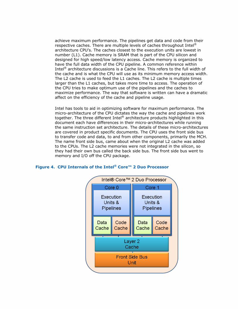
achieve maximum performance. The pipelines get data and code from their respective caches. There are multiple levels of caches throughout Intel® architecture CPU’s. The caches closest to the execution units are lowest in number (L1). Cache memory is SRAM that is part of the CPU silicon and designed for high speed/low latency access. Cache memory is organized to have the full data width of the CPU pipeline. A common reference within Intel® architecture discussions is a Cache line. This refers to the full width of the cache and is what the CPU will use as its minimum memory access width. The L2 cache is used to feed the L1 caches. The L2 cache is multiple times larger than the L1 caches, but takes more time to access. The operation of the CPU tries to make optimum use of the pipelines and the caches to maximize performance. The way that software is written can have a dramatic affect on the efficiency of the cache and pipeline usage.
Intel has tools to aid in optimizing software for maximum performance. The micro-architecture of the CPU dictates the way the cache and pipelines work together. The three different Intel® architecture products highlighted in this document each have differences in their micro-architectures while running the same instruction set architecture. The details of these micro-architectures are covered in product specific documents. The CPU uses the front side bus to transfer code and data, to and from other components, primarily the MCH. The name front side bus, came about when the original L2 cache was added to the CPUs. The L2 cache memories were not integrated in the silicon, so they had their own bus called the back side bus. The front side bus went to memory and I/O off the CPU package.
Figure 4. CPU Internals of the Intel® Core™ 2 Duo Processor

10 321087
The Front Side Bus
The front side bus (FSB) is the interface that the CPU uses to access information outside of its own package. The FSB is implemented in two electrical types. The more common type uses Gunning Transistor Logic (GTL), the newer implementation used on the Intel® Atom™ family of CPUs uses CMOS drivers. The GTL FSB utilizes an open drain type driver that necessitates a termination resistance for each pin. Over the years, Intel has integrated these termination resistors into the silicon for most of the pins. The GTL interface allows for more than two devices to share the same bus. Intel® Xeon® Processors make use of this capability to allow up to four CPU devices paired to one memory controller with dedicated and independent FSBs. Reference the corresponding Platform Design Guide document for the implementation details of any given Intel® CPU. The FSB has evolved through the generations of Pentium® and Intel® Core™ CPUs.
Figure 5. FSB Basics
In the current implementation, the timing control for data being read and written on the FSB uses source synchronous clocking. In this approach, there are dedicated strobe signals that are sent synchronously with address and data from the originating device. This makes the high clock speeds of the FSB feasible (up to 400MHz). The strobes will run at multiples of the base clock frequency which allows the address to be double clocked or pumped, and the data to be quad pumped. The FSB speed is commonly referenced by the throughput rate and not the base clock rate due to the quad pumping of data

(e.g., 1333 Mega Transfers per second (MT/s) is based on a 333 MHz base clock).
The FSB uses dedicated address, data, strobes, and request pins. The data width is 64 and the number of address pins varies from 32 to 40 depending on the class of CPU. The FSB request pins are used to signify different phases of a given read or write operation. The request pins are also used to signify cache coherency status for a given FSB transaction. One of the operations that will occur on the FSB will be to maintain the coherency of the contents of CPU cache and the system memory. These coherency operations occur automatically as software executes and data is moved to and from memory by the CPU or by an I/O device. The bus is pipelined and supports split transactions. This improves command bandwidth by allowing new requests to be issued before previous transactions complete.
CPU Side Band Signals
There are other signals on the CPU besides the FSB. These signals as a group are referred to as side band signals. These signals have various control and interrupt functions. Most of the side band signals also use the GTL type driver. Some of the sideband signals will be discussed in this article, but the Platform Design Guide must be used to ensure proper usage of all the side band signals on a given design. The component data sheets must also be referenced to understand voltage compatibilities for these pins. One type of control signal group on the CPU is called the voltage identification pins (VID). Intel has defined voltage regulator standards that make use of the VID pins to allow the CPU to request the voltage that it wants. The VIDs are dynamic as the voltage requested can change based on the internal frequencies, the power state, or as a mechanism to reduce CPU temperature.
Memory Controller
The central hub for the data traffic in an Intel® architecture system is the Memory Controller Hub (MCH). Until the new Intel® Atom™ and Intel® Core™ i7 architectures were developed, the MCH had been a discrete component. The Intel® Core™ 2 Duo architecture uses a discrete MCH which will be described first. Figure 6 shows the MCH for a system featuring the Intel® Core™ 2 Duo processor. The MCH facilitates the transfer of data to and from all the interfaces. When the BIOS configures the MCH, it defines the base address locations for all the interfaces. The BIOS relays the configuration information to the operating system so it knows the capabilities and locations of the hardware that is in its system.
There are many different models of MCH currently offered by Intel. The feature differences between MCH’s include the number and type of memory channels, the number of PCIe* lanes supported, internal 2D/3D graphics, single or multiple CPU support (uni-processor (UP) or dual-processor (DP) or

12 321087
multi-processor (MP)). Intel validates specific CPU’s with specific MCH’s to provide a well balanced platform. Not all CPU FSB speeds are compatible with all MCH’s.
Figure 6. Intel® MCH Internals
PC
I Express*
Front Side BusUnit
Intel® MCH
DMIM
emor
y C
ontr
olle
r
Data Steering
and Arbitration
iGFX
PC
I Express*
PC
I Express*
Front Side BusUnit
Front Side BusUnit
Intel® MCH
DMIDMIM
emor
y C
ontr
olle
rM
emor
y C
ontr
olle
r
Data Steering
and Arbitration
Data Steering
and Arbitration
iGFXiGFX
The CPU connects to the MCH through the FSB which was described earlier. The FSB unit in the MCH is responsible for the CPU cache coherency. If data at the address requested is not in the CPU cache, or the data in memory is newer, the memory controller is told to retrieve the data at that address. Data transfers between the CPU and memory are always 64 bits, the full width of the L2 cache on the CPU. If only a byte of data is requested, the full 64 bits is retrieved but the CPU will only use 8 of those bits. The memory controller is configurable by the BIOS to support multiple speeds and sizes of memory. The refreshing of the DRAM is handled by the memory controller after it’s initially configured. The specific type, size, and speed of memory that is supported, varies by the model of MCH.
The Direct Media Interface (DMI) interface in the MCH is a dedicated serial link to the I/O Controller Hub (ICH). The DMI link is actually four serial links, with dedicated transmit and receive pins. These serial links are referred to as “lanes” and all use differential signaling. So the DMI is 4 lanes x Transmit and Receive (2) x differential signaling (2) = 32 pins. The DMI usage will be described in a separate section. DMI supports signaling of 2.5GT/s.

The PCI Express* (PCIe*) interface is the highest bandwidth I/O interface in the IA system. The number of PCIe lanes can vary depending on the MCH used, but will usually be in multiples of 8. A common width for PCIe is 16 lanes as this is the maximum width for discrete PCIe graphics cards. The PCIe interface uses the same differential signaling that the DMI does, but PCIe supports higher transfer rates. The original PCIe specification states data rates of 2.5Gb/s per lane (this what DMI uses). The second generation of PCIe is now available and doubles the data rate to 5Gb/s.
Many of the MCH versions also have internal graphics controllers. The details of the graphics controllers won’t be covered in this document, but the basic capabilities are 2D and 3D acceleration. The types of display interfaces directly supported by MCH’s varies by the model.
I/O Controller
The I/O Controller Hub (ICH) provides extensive I/O support, support for legacy peripherals dating back to the 1980s, and integrates support for key platform management functions such as power sequencing and ACPI power management, fan speed control, and reset timing. It will be seen that these later functions are critical to system operation and often overlooked by designers.
Figure 7. Intel® ICH Internals
LPCLPC
Intel® ICH
DMISATASATA
USBUSBRTCRTC
PCIe*PCIe*
Timers / InterruptsTimers /
Interrupts
GPIOGPIO
Power Management
Power Management
InternalBusesInternalBuses
LANLAN AudioAudio
SPISPI
IDEIDELPCLPC
Intel® ICH
DMIDMISATASATA
USBUSBRTCRTC
PCIe*PCIe*
Timers / InterruptsTimers /
Interrupts
GPIOGPIO
Power Management
Power Management
InternalBusesInternalBuses
LANLAN AudioAudio
SPISPI
IDEIDE
As the ICH is used to control the reset sequence, and often power sequencing of the other system components, it has power supplies which are required to

14 321087
turn on before the rest of the system. Also, the Real Time Clock (RTC) needs to have a 32.768KHz oscillator running before to properly sequence. The ICH communicates with the IOH/MCH during reset and power cycling events to try to make these events “safer”. For example, a warning message will be sent over DMI before a reset to allow SMBUS or memory transactions to complete before the reset.
Modern I/O Interfaces
The ICH acts a bridge or controller for a variety of industry standard interfaces allowing the system designer to chose from a wide range of peripherals.
• PCI interface operates at 33MHz and allowing for a number of external bus masters. The ICH acts as the central arbiter and root of the PCI bus.
• PCI Express* root port controllers. The number of ports varies with the product but is generally in the range of 1 to 4. Link widths of x1 x4 are support at speeds of 2.5GB/s.
• Serial ATA (SATA) controllers supporting both legacy operation using I/O space and the Advanced Host Controller Interface (AHCI) using memory mapped I/O as well as allowing advanced features such has hot-plug and native command queuing. SATA II supports data rates of 1.5Gb/s and 3Gb/s.
• Integrated Drive Electronics (IDE) controllers are also used to control hard disc drives, and CD/DVD drives. They have been replaced in some platforms by the newer SATA interface since it offers better performance over a smaller interface.
• Universal Serial Bus (USB) supporting High Speed USB 2.0 (480 Mb/s) operation as well as full-speed (12 Mb/s) and low-speed signaling.
• General Purpose I/O (GPIO) pins for system customization. Many pins can also be configured to cause interrupts or wake events.
• System Management Bus (SMBus 2.0) The SMBus Host interface allows the processor to communicate with SMBus slaves. This interface is also compatible with most I2C devices. Slave functionality, including the Host Notify protocol is implemented. Hence, the host controller supports eight command protocols of the SMBus interface (see System Management Bus (SMBus) Specification, Version 2.0): Quick Command, Send Byte, Receive Byte, Write Byte/Word, Read Byte/Word, Process Call, Block Read/Write, and Host Notify.
• Serial Peripheral Interface (SPI) is used to interface to BIOS flash devices which contain the boot firmware and initialization code. Up to 2 SPI flash devices operating at 33 MHz can be connected. Note that the flash devices connected to the LPC interface are quickly becoming

obsolete and SPI is expected to be standard interface for BIOS flash in the future. The ICH is always a master on the SPI interface.
• Low Pin Count Interface (LPC) This interface replaces the ISA bus originally developed by IBM in the early 1980s, but uses only 7 signals plus a clock. It can be used to connect to a variety low speed devices that don’t require the bandwidth of PCI or PCI Express*. This interface is typically used to interface with Super I/O devices which contain many interfaces such as floppy driver controller, PS2 keyboard/mouse controls and serial ports.
• JTAG Boundary Scan allows testing of PCB board after assembly.
Support Peripherals
The ICH integrates numerous support peripherals that replace many external components.
• Real Time Clock (RTC): The RTC is compatible with the Motorola MC146818A*. It contains 256 bytes of RAM that can be maintained with a 3V battery. 242 bytes are available for use while the remaining are dedicated to the clock function. The RTC supports generating wake events up to 30 days in the future. An external 32.768 KHz crystal is required for operation.
• High Precision Event Timers These are high resolution timers which can be used to generate periodic or one-shot interrupts. There are 8 comparators which share a common counter that is clocked from a 14.31818 MHz source.
• Advanced Programmable Interrupt Controller (APIC) is a more modern interrupt controller than the 82C59 (see below). It supports multiprocessor/multi core interrupt management and allows interrupts to be directed to a specific processor. The I/O APIC in the ICH can support up to 24 interrupt vectors and can work in conjunction with I/O APICs in other devices (such as the IOH) to help eliminate the need for multiple device to share interrupts.
Compatibility Peripherals
The ICH contains peripherals that date back to the earliest IBM* PCs which used the Industry Standard Architecture (ISA) bus. The ISA bus has been replaced by the Low Pin-Count (LPC) bus in modern systems, but the peripherals that were once discrete components are now integrated into the ICH. One key strength of Intel® architecture is maintaining backward compatibility while continuing to innovate.
The ICH contains two 82C37 DMA controllers, two ISA-Compatible 82C59 interrupt controllers and three 82C54 programmable interval timer equivalents.

16 321087
The 82C37 DMA controllers should not be confused with the DMA engines found in some MCHs. These DMA controllers are tied to the ISA/LPC bus and used mostly for transfers to/from slow devices such as Floppy Disk Controllers.
The ISA compatible 82C59 interrupt controllers have been largely supplanted by the Advanced Programmable Interrupt Controller (APIC) since it offers support for more than 15 interrupt sources and supports multi-core/multi-processor systems. However, the 82C59 controllers are still used by some older operating systems which run only on uni-processor (single CPU) systems.
The I/O Controller Hub (ICH) in an Intel® architecture system provides interfaces to lower speed I/Os and also integrates a lot of system control functions. One unique aspect of the ICH is that it should get power before the other IA components. The ICH controls the power states of the system and also provides the system reset signal. A typical PC type application will also utilize the ICH for the real-time-clock (RTC). The RTC uses a coin cell battery and a 32 KHz oscillator in the system to keep time and date information. The ICH also uses the battery to keep a small SRAM valid for system setting parameters that are user configurable (this is the CMOS settings provided through the BIOS setup).
The ICH provides numerous I/O interfaces including 32-bit PCI, USB, SATA, extra PCIe* lanes, general purpose I/O pins and SMBus. The ICH has two interfaces for connection of the BIOS device (usually Flash EPROM). One is the Low Pin Count Bus (LPC), the second is a Serial Peripheral Interface (SPI). The LPC is a 33 MHz 4 bit bus that can be used for numerous low speed devices. Besides the BIOS Flash, the LPC can be used for other devices such as a micro controller, a security device, or a Super I/O. A Super I/O is a device that integrates much of legacy I/O, like serial ports, parallel printer, floppy drive controller, keyboard and mouse interfaces and others, into a single device. The ICH also has timers, interrupt controllers and an interface to the BIOS device. Some versions of ICH have other features like audio and Ethernet controllers. The ICH has state machines that respond to external signals to control power and reset. Many of the internal addresses in the ICH are fixed. This allows the BIOS and applications to always find the minimum system components needed to start up an Intel® architecture system.
What is a BIOS?
The Intel® architecture system relies on firmware that is always at the CPU reset vector (which is FFFFFFF0h but appears on the FSB as FFFFFFFC0h as a full cache line is read). This firmware is known as the Basic Input/Output System (BIOS). The BIOS controls the activity of the Intel® architecture hardware until the operating system takes over. One job of the BIOS is to configure registers throughout the Intel® architecture components that set up the devices to the particulars of the system hardware into which the Intel®

architecture is designed. In a typical PC design, some of the hardware is dedicated by the design based on the motherboard design, but other hardware aspects vary based on what the end user may plug into the motherboard. As the BIOS executes, after the initial configuration is done, it will determine the type and amount of memory, then it goes through a discovery phase. Once all the devices and hardware are configured the BIOS will turn over control of the system to an operating system.
Intel® Core™ i7 Architecture
The Intel® CoreTM i7 Processor
The Intel® Core™ i7 Processor is a new micro architecture based on a 45 nm process and designed to deliver high performance with power efficiency. It introduces several new technologies and features:
• Integrated 3-channel DDR3 memory controller supporting up to 1333 MT/s operation. The memory controller offers measured bandwidth in excess of 28 GB/sec and low latency.
• L2 cache per core. This cache sits between the dedicated L1 cache and the shared L3 cache.
• A new point-to-point link based interface called Intel® QuickPath Interconnect. This interface replaces the front side bus of other architectures.
• Up to four cores with Simultaneous Multi-Threading (SMT). SMT allows a physical core to appear as two logical cores to software.
Figure 8. Intel® Core™ i7 Internals

18 321087
Intel® QuickPath Interconnect
The Intel® QuickPath Interconnect is a new high speed link based bus which replaces the Front Side Bus. It offers higher bandwidth, better reliability and requires fewer pins compared to the FSB. All the sideband signals have been removed and replaced with inband messages.
Figure 9. Intel® QuickPath Interconnect Basics
Intel® QuickPath Interconnect
CPUHigh Speed
I/OController
IOH
Forwarded Clock – 1 diff pair
Control/Data Link – 20 diff pairs
Forwarded Clock – 1 diff pair
Control/Data Link – 20 diff pairs
Intel® QuickPath Interconnect
CPUCPUHigh Speed
I/OController
High Speed I/O
Controller
IOHIOH
Forwarded Clock – 1 diff pair
Control/Data Link – 20 diff pairs
Forwarded Clock – 1 diff pair
Control/Data Link – 20 diff pairs
Intel® QuickPath Interconnect uses high speed differential signaling with a forwarded clock topology. The signaling levels are similar to PCI Express*, but the protocol is unique and supports coherency. It supports transfer rates up to 6.4GT/S in each direction and so has a peak bandwidth of about 2.5x the fastest FSB implementation.
A full-width link is comprised of 20 differential pairs plus a forwarded clock. Data is transferred in 80-bit chunks called Flits (Flow Control Units). An 8-bit CRC protects 72-bits of payload/control. Corrupted Flits are automatically re-tried. This improves system reliability over FSB systems where errors where catastrophic events.

The IOH
The Input/Output Hub or IOH is a new system component introduced with the Intel® Core™ i7 processor. The Intel® X58 Express Chipset is the first component with the IOH designation and replaces the MCH in some respects. The IOH primarily serves as a switch between the processor’s Intel® QuickPath Interconnect and several PCI Express* ports. It maintains proper ordering of transactions and provides for fair arbitration between ports. The DMI link is reserved for communication to the Intel® ICH.
There are different IOHs supporting a number of different PCI Express* and platform configurations.
Figure 10. IOH Internals
• Intel® Quick Path Interconnect controller acts as a caching agent on the Intel® QPI fabric. It is responsible for translating between Intel® QPI and PCI Express* protocols and helps to maintain cache coherency in the platform.
• PCI Express* Root Port Controllers. There are two x16 and one x4 port which are capable of running up to Gen 2 speeds (5 Gbs). The x16 ports can bifurcate to 2x8 or 4x4 while the x4 port can bifurcate

20 321087
to 2x2. All ports can train to a x1 link as required in the PCI Express* specification. The PCI Express ports support peer-to-peer traffic.
• Vtd-2 engine assists with the virtualization of I/O devices. The Vtd-2 engine performs address translations and access right checks on inbound PCIe* requests. Addresses are translated from guest physical addresses to host physical addresses. This allows I/O devices to deal only with guest physical addresses.
• IOAPIC acts as an interrupt controller for the IOH. It handles interrupts from internal sources (such as DMA engines) as well as PCI Express* devices. PCI Express devices are also free to use MSI/MSI-X type interrupts where interrupts are requested by writing to a set of dedicated memory addresses.
Intel® Atom™ Architecture The recently released Intel® Atom™ architecture utilized the same basic data flows as the Intel® Core™ 2 Duo architecture, but instead of just the MCH and ICH, the Intel® Atom™ processor can connect to a System Controller Hub (SCH). The SCH integrates most of the MCH and ICH functionality into one device that optimizes the interfaces for ultra low power applications. The target markets for the SCH do not require the same number of ports on each interface that the ICH can provide. For designs based on the Intel® Atom™ processor, there is also a version of the MCH/ICH that can work with the Intel® Atom™ CPU to provide the large quantity of I/O ports, if it is needed. The SCH provides a similar power management role as the ICH and should be powered first.

Figure 11. Intel® SCH Internals
LPCLPC
Intel® SCH
FSB(CMOS)
IDEIDE
USBUSB
RTCRTC PCIe*PCIe*
Timers / InterruptsTimers /
Interrupts
GPIOGPIO
Power Management
Power Management
InternalBuses
InternalBuses
LANLANHD
AudioHD
Audio
SPISPI
MemoryControllerMemory
Controller
GraphicsSDVO / LVDS
GraphicsSDVO / LVDS
SDIO / MMC
SDIO / MMC
LPCLPC
Intel® SCH
FSB(CMOS)FSB(CMOS)
IDEIDE
USBUSB
RTCRTC PCIe*PCIe*
Timers / InterruptsTimers /
Interrupts
GPIOGPIO
Power Management
Power Management
InternalBuses
InternalBuses
LANLANHD
AudioHD
Audio
SPISPI
MemoryControllerMemory
Controller
GraphicsSDVO / LVDS
GraphicsSDVO / LVDS
SDIO / MMC
SDIO / MMC
The I/O and peripheral interface differences between the ICH and SCH are listed below.
• SDIO Secure Digital Input / Output – Usually used for media cards.
• MMC Multi-Media Card – Usually used for media cards.
• SDVO Serial Digital Video Out – display interface.
• LVDS Low Voltage Digital Signaling – flat panel display interface.
The Intel® Atom™ processor design is optimized for very low power consumption. The voltage levels are lower and the speed of the FSB is lower than the Intel® Core™ 2 Duo. The lower speed FSB allows CMOS drivers to be used which draw less power than the GTL drivers. Another capability of the Intel® Atom™ CPU is to dynamically reduce on chip cache size to save power. The SCH has many advanced power management capabilities to enable the lowest possible platform power consumption.
Tools for New Designs This section gives an overview of some reference documentation available to help with an Intel® architecture design. Many of these documents are

22 321087
available on http://developer.intel.com/design/index.htm. Others will require a Non-Disclosure agreement and will be made available through your sales representative.
Platform Design Guide is available under Non-Disclosure Agreement and gives detailed PCB design recommendation including PCB stack-up, impedance targets, material selection and layout recommendations.
Platform Reference Schematics given an example system implantation.
Thermal and Mechanical Design Guide covers heatsink design recommendations and package/socket attachment to the printed circuit board.
Datasheets (Processors) contain electrical, thermal and package mechanical information for Intel processors.
Datasheets (MCH/IOH/ICH) contains a functional and register description of the device. Pinout and package mechanical information is also included. Electrical specifications may be in the datasheet or might require a Non-Disclosure Agreement.
Intel® 64 and IA-32 Architectures Software Developer’s Manuals These manuals describe the architecture and programming environment of the Intel® 64 and IA-32 processors.
Specification Updates contain lists of errata and the most recent changes to the other documents. Specification updates should always be consulted for the latest available information.
Intel Packaging Databook is intended to serve only as a data reference guide to Intel package selection and availability. As the packaging landscape changes very rapidly, information can become outdated very quickly. Please refer to the product specifications on the Products site for the most current detailed package information.
ITP – In Target Probe
Intel utilizes a serial interface to its major components that provides a background interface to the operation of the device. This was originally created for internal testing, but later was made available to everyone. Intel has enabled a third party vendor with the details of the ITP interface and they have developed tools that are very useful for hardware checkout and software development. For information on ITP tools contact American Arium* (www.arium.com).
Conclusion The Intel= architecture products offer a great span of features, performance, and power levels. The ability to reuse software across generations and product families is a great benefit and gives designs the ability to scale performance and features without new software re-writes. The basic building blocks of an Intel® architecture system are highly integrated and make system design as straightforward as possible. Intel provides all of the resources necessary to design leading edge products, so go to www.intel.com and start creating.
References
Intel® CPU History http://www.intel.com/pressroom/kits/quickreffam.htm
Intel® Developers Website http://developer.intel.com/design/index.htm
American Arium* http://www.arium.com

24 321087
Authors
Todd Langley is a Systems Engineer with the Embedded Communications Group at Intel Corporation.
Rob Kowalczyk is a Technical Marketing Engineer with the Embedded Communications Group at Intel Corporation.
Acronyms
CPU Central Processing Unit
DMI Direct Media Interface
FSB Front Side Bus
ICH Input / Output Control Hub
IOH Input / Output Hub
MCH Memory Controller Hub
SCH System Controller Hub
QPI Quick Path Interconnect

INFORMATION IN THIS DOCUMENT IS PROVIDED IN CONNECTION WITH INTEL® PRODUCTS. NO LICENSE, EXPRESS OR IMPLIED, BY ESTOPPEL OR OTHERWISE, TO ANY INTELLECTUAL PROPERTY RIGHTS IS GRANTED BY THIS DOCUMENT. EXCEPT AS PROVIDED IN INTEL’S TERMS AND CONDITIONS OF SALE FOR SUCH PRODUCTS, INTEL ASSUMES NO LIABILITY WHATSOEVER, AND INTEL DISCLAIMS ANY EXPRESS OR IMPLIED WARRANTY, RELATING TO SALE AND/OR USE OF INTEL PRODUCTS INCLUDING LIABILITY OR WARRANTIES RELATING TO FITNESS FOR A PARTICULAR PURPOSE, MERCHANTABILITY, OR INFRINGEMENT OF ANY PATENT, COPYRIGHT OR OTHER INTELLECTUAL PROPERTY RIGHT. Intel products are not intended for use in medical, life saving, or life sustaining applications.
Intel may make changes to specifications and product descriptions at any time, without notice.
This paper is for informational purposes only. THIS DOCUMENT IS PROVIDED "AS IS" WITH NO WARRANTIES WHATSOEVER, INCLUDING ANY WARRANTY OF MERCHANTABILITY, NONINFRINGEMENT, FITNESS FOR ANY PARTICULAR PURPOSE, OR ANY WARRANTY OTHERWISE ARISING OUT OF ANY PROPOSAL, SPECIFICATION OR SAMPLE. Intel disclaims all liability, including liability for infringement of any proprietary rights, relating to use of information in this specification. No license, express or implied, by estoppel or otherwise, to any intellectual property rights is granted herein.
BunnyPeople, Celeron, Celeron Inside, Centrino, Centrino logo, Core Inside, Dialogic, FlashFile, i960, InstantIP, Intel, Intel logo, Intel386, Intel486, Intel740, IntelDX2, IntelDX4, IntelSX2, Intel Core, Intel Inside, Intel Inside logo, Intel. Leap ahead., Intel. Leap ahead. logo, Intel NetBurst, Intel NetMerge, Intel NetStructure, Intel SingleDriver, Intel SpeedStep, Intel StrataFlash, Intel Viiv, Intel vPro, Intel XScale, IPLink, Itanium, Itanium Inside, MCS, MMX, Oplus, OverDrive, PDCharm, Pentium, Pentium Inside, skoool, Sound Mark, The Journey Inside, VTune, Xeon, Xeon Inside, Intel Core, and Intel Atom are trademarks or registered trademarks of Intel Corporation or its subsidiaries in the United States and other countries.
*Other names and brands may be claimed as the property of others.
Copyright © 2008 Intel Corporation. All rights reserved.
§