introduction - 123seminarsonly.com · chapter-1 introduction are you tired of slow modem...
TRANSCRIPT

CHAPTER-1
INTRODUCTION
Are you tired of slow modem connections? Cellonics Incorporated has developed new
technology that may end this and other communications problems forever. The new modulation
and demodulation technology is called Cellonics. In general, this technology will allow for
modem speeds that are 1,000 times faster than our present modems. The development is based
on the way biological cells communicate with each other and nonlinear dynamical systems
(NDS). Major telcos, which are telecommunications companies, will benefit from the incredible
speed, simplicity, and robustness of this new technology, as well as individual users.
In current technology, the ASCII uses a combination of ones and zeros to display a single
letter of the alphabet (Cellonics, 2001). Then the data is sent over radio frequency cycle to its
destination where it is then decoded. The original technology also utilizes carrier signals as a
reference which uses hundreds of wave cycles before a decoder can decide on the bit value
(Legard, 2001), whether the bit is a one or a zero, in order to translate that into a single character.
The Cellonics technology came about after studying biological cell behaviour. The study showed
that human cells respond to stimuli and generate waveforms that consist of a continuous line of
pulses separated by periods of silence. The Cellonics technology found a way to mimic these
pulse signals and apply them to the communications industry (Legard, 2001). The Cellonics
element accepts slow analog waveforms as input and in return produces predictable, fast pulse
output, thus encoding digital information and sending it over communication channels.
Nonlinear Dynamical Systems (NDS) are the mathematical formulations required to simulate the
cell responses and were used in building Cellonics. Because the technique is nonlinear,
performance can exceed the norm, but at the same time, implementation is straightforward
(Legard, 2001).
AIET/DOECE/2010/SP/1

This technology will be most beneficial to businesses that do most of their work by remote and
with the use of portable devices. The Cellonics technology will provide these devices with faster,
better data for longer periods of time (Advantages, 2001). Cellonics also utilizes a few discrete
components, most of which are bypassed or consume very little power. This reduces the number
of off the shelf components in portable devices while dramatically decreasing the power used,
leading to a lower cost for the entire device. The non-portable devices of companies will benefit
from the lack of components the machines have and the company will not have to worry so much
about parts breaking.
AIET/DOECE/2010/SP/2

CHAPTER- 2
PRINCIPLE OF CELLONICS TECHNOLOGY
Fig 2.a: Measured ß-cell Response
The Cellonics™ technology is a revolutionary and unconventional approach based on the theory
of nonlinear dynamical systems (NDS) and modelled after biological cellbehaviour1. In essence,
the term Cellonics is an euphemism for ‘electronic cells’. When used in the field of
AIET/DOECE/2010/SP/3

communications, the technology has the ability to encode, transmit and decode digital
information powerfully over a variety of physical channels, be they cables or wirelessly through
the air. There has been much research over the past decades to study inter-cell communications.
Laboratory studies have recorded electrical waveforms that show burst of spikes separated by
periods of silence
Fig 2.b: Waveforms
For examples, Fig 2a and Fig 2b show the behaviour of the ß-cell and the Leech Nociceptor
respectively. From these figures, we may observe that the slow waveforms2 trigger the fast pulse
trains3 allowing the cells to convey information (as postulated by some researchers).Note that
while the fast pulse trains are always the same, the slow time-varying stimulus analog
waveforms can take many arbitrary shapes. The number of the pulse trains varies according to
the parameters of the slow analog waveforms. Thus, if a circuit can be found that accept an
analog input waveform and output a set of pulse trains with predictable number of pulses in each
burst, we have a very powerful means of encoding digital information and communicating it over
a variety of physical channels. Cellonics Inc. has invented and patented a number of circuits that
mimic the above biological cell behaviour. The Cellonics™ circuits are incredibly simple with
advantages of low-cost, low power consumption and smallness of size. They can and have been
used in various applications such as communications and electronic circuits (gated oscillator,
sigma delta modulator, delta modulator, clock multipliers, etc). When applied in
communications, the Cellonics™ technology is a fundamental modulation and demodulation
technique. The Cellonics™ receivers are used as devices that generate pulses from the received
analog signal and perform demodulation based on pulse counting and related algorithms.
AIET/DOECE/2010/SP/4

1 The study of biological cell behaviour is ONLY an inspiration to the invention of Cellonics™
circuits. The Cellonics™ technology is NOT related to any neural network communications or
neurophomic electronics.
2 Slow waveforms: Analogue waveforms that vary slowly with time. These waveforms can be in
any arbitrary shape.
3 Fast waveforms/fast pulse trains: Waveform in the shape of pulses that varies rapidly with time
AIET/DOECE/2010/SP/5

CHAPTER- 3
CELLONICS CIRCUITS
Cellonics Inc. has developed and patented families of Cellonics™ circuits that are useful for
various applications. One of these Cellonics™ circuits is an extremely simple circuit that
exhibits the “Scurve” transfer characteristic. Fig 3a shows one of the possible circuit realizations.
The circuit contains a negative impedance converter. Its I-V transfer characteristic is shown in
Fig 3b.Thetransfer characteristic consists of three different regions. The two lines at the top and
bottom have positive slope, 1/RF and they represent the regions in which the Op-Amp is
operating in the saturated (nonlinear) mode. In Fig 3b, the middle segment has a negative slope
(negative resistance)
Fig 3.a: Cellonics Circuit
AIET/DOECE/2010/SP/6

Fig 3b: Phase Space & I-V Characteristics Curve
and represents the region in which the Op-Amp is operating linearly. It is this negative resistance
region that allows the Op-Amp to oscillate and produce pulses bounded by the positive and
negative saturation voltages.
For ease of explanation4, we assume that the input signal is a triangular waveform. Here we have
dVs/dt = (V0 depending on the slope of the triangular input waveform. Whenever the slope is
positive, the Op-Amp is stable and outputs a constant saturation voltage. Thus a silent period is
observed i.e. no spike is being produced. On the other hand, with properly selected circuit
parameters whenever the slope of the triangular waveform is negative, the Op-Amp is unstable.
In this region, the output is oscillating. The duration of each pulse is similar and the number of
pulses generated depends on the length of time the slope remains negative. Thus by Controlling
the duration of the negative slope, he number of pulses to be produced at the output of the Op-
Amp can be controlled. The Cellonics™ circuit is robust against noise perturbations – as long as
the effective negative slope keeps the Op-Amp unstable, the noise will not have an effect on the
pulse generation. The level of tolerance against the noise perturbations is carried out by proper
AIET/DOECE/2010/SP/7

selection of circuit parameters in the design. There are also many other families of Cellonics™
circuits. By using the Principle of Duality, the “N-curve” families of Cellonics™ circuits can be
derived. In this case, the realization of the circuits can be based on the OP-AMP or devices such
as he tunnel diode, etc. The transfer function of a tunnel diode exhibits the “N- curve” transfer
characteristic inherently, which is a “dual” of the S-curve” family. By connecting an inductor
and
Fig 3c: PN-Curve Cellonics™ Element
a tunnel diode in series, we can produce pulses that are separated by periods of silence. This
family of circuits responds to the voltage level of the input signal. As an application example, a
square wave signal is used in Fig 3c. In this case, the duration when the input signal is above a
certain “threshold” voltage determines the duration that the circuit operates in the unstable region
and consequently the number of pulses generated.
AIET/DOECE/2010/SP/8
CHAPTER- 4
APPLICATIONS TO TELECOMMUNICATIONS
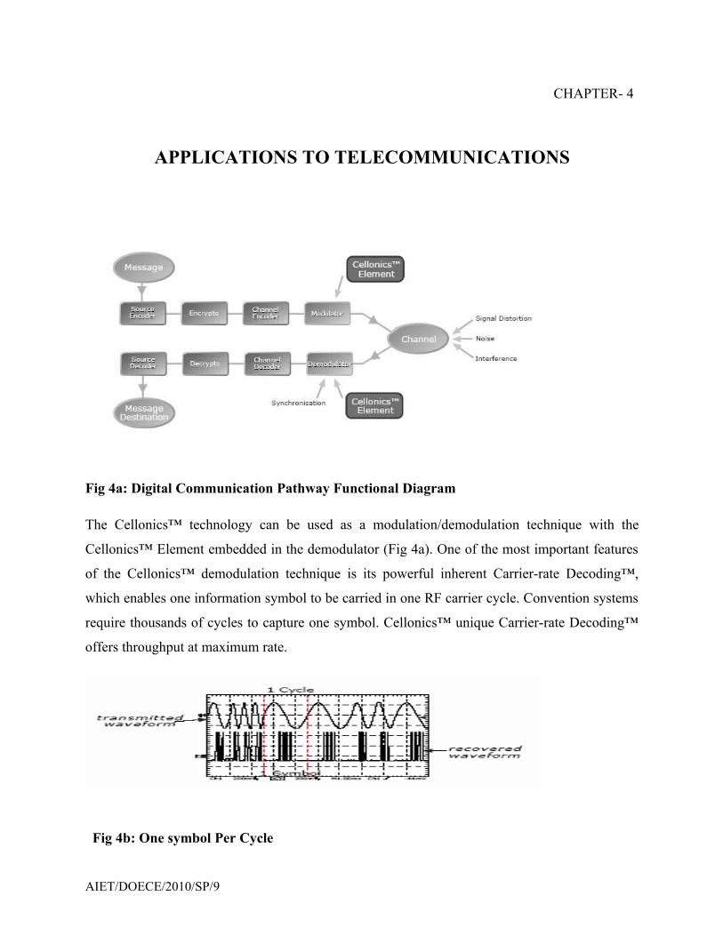
Fig 4a: Digital Communication Pathway Functional Diagram
The Cellonics™ technology can be used as a modulation/demodulation technique with the
Cellonics™ Element embedded in the demodulator (Fig 4a). One of the most important features
of the Cellonics™ demodulation technique is its powerful inherent Carrier-rate Decoding™,
which enables one information symbol to be carried in one RF carrier cycle. Convention systems
require thousands of cycles to capture one symbol. Cellonics™ unique Carrier-rate Decoding™
offers throughput at maximum rate.
Fig 4b: One symbol Per Cycle
AIET/DOECE/2010/SP/9
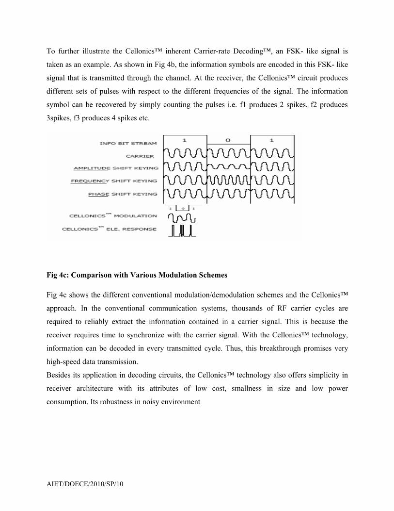
To further illustrate the Cellonics™ inherent Carrier-rate Decoding™, an FSK- like signal is
taken as an example. As shown in Fig 4b, the information symbols are encoded in this FSK- like
signal that is transmitted through the channel. At the receiver, the Cellonics™ circuit produces
different sets of pulses with respect to the different frequencies of the signal. The information
symbol can be recovered by simply counting the pulses i.e. f1 produces 2 spikes, f2 produces
3spikes, f3 produces 4 spikes etc.
Fig 4c: Comparison with Various Modulation Schemes
Fig 4c shows the different conventional modulation/demodulation schemes and the Cellonics™
approach. In the conventional communication systems, thousands of RF carrier cycles are
required to reliably extract the information contained in a carrier signal. This is because the
receiver requires time to synchronize with the carrier signal. With the Cellonics™ technology,
information can be decoded in every transmitted cycle. Thus, this breakthrough promises very
high-speed data transmission.
Besides its application in decoding circuits, the Cellonics™ technology also offers simplicity in
receiver architecture with its attributes of low cost, smallness in size and low power
consumption. Its robustness in noisy environment
AIET/DOECE/2010/SP/10

Fig 4d: 4th Generation GSM Receiver Architecture vs. Cellonics™
also offers a system that has better performance and receiver sensitivity. Fig 4d
shows a conventional Super heterodyne receiver which is complex in design and has many
practical drawbacks. Some issues that need considerable attention include: device noise inter
modulation, local oscillators/mixer isolation, Phase Lock Loop (PLL) switching time and noise
immunity. Moreover, these subsystems consume considerable amount of power. A newer
technique uses the Super homodyne approach with no IF stage (i.e. zero-IF). But these solutions
are difficult to manufacture, have some tricky problems (e.g. DC offset) and still require power
hungry subsystems as mentioned earlier. With the Cellonics™ technology, a very simple
receiver architecture can be realized without oscillators, phase lock loops etc. This is a paradigm
shift in design.
AIET/DOECE/2010/SP/11

Fig 4e: 4th Generation GSM Receiver vs. Cellonics
Fig 4e shows a more detailed diagram of the 4thgeneration Super homodyne GSM receiver and
the Cellonics™ receiver. It clearly shows the simplicity of the Cellonics™ receiver as no
oscillators and crystals are required. To improve the spectral efficiency, multi-level
Fig 4f: Other Performance Advantages
modulation scheme is usually employed. Fig 4fcompares a conventional M-ary FSK receiver and
a Cellonics™ receiver. Each increase in the modulation level requires a significant number of
AIET/DOECE/2010/SP/12
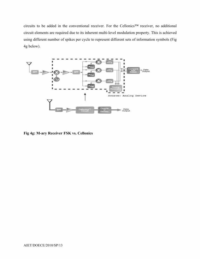
circuits to be added in the conventional receiver. For the Cellonics™ receiver, no additional
circuit elements are required due to its inherent multi-level modulation property. This is achieved
using different number of spikes per cycle to represent different sets of information symbols (Fig
4g below).
Fig 4g: M-ary Receiver FSK vs. Cellonics
AIET/DOECE/2010/SP/13

CHAPTER 5
PERFORMANCE OF CELLONICS ™ RECEIVER
Fig 5a: Cellonics™ Receiver Performance
5.A- BER Performance in a Narrowband Communication System
An important performance measure of any modulation scheme is its bit-error rate (BER)
performance in a noisy channel. Fig 5a shows the numerical simulation results of the Cellonics™
receiver in the AWGN channel. Also shown in the figure is the theoretical curve of the optimal
Binary Phase Shift Keying (BPSK) modulation scheme. From the figure, it is clear that the BE
performance of the Cellonics™ modulation is able to match the theoretical optimal BPSK
modulation scheme. This is achieved by using only 4Cellonics™ elements which are very simple
(please refer to Fig 3a and Fig 3d). Figure 5b shows another set of results in the multi-path
environment which show that the Cellonics™
Fig 5b: Performance in 2-path and AWGN Channel
AIET/DOECE/2010/SP/14
receiver has similar performance as the BPSK receiver but with much simpler receiver
architecture. Furthermore, in practical terms, the Cellonics™ receiver will have less
implementation losses when compared to a conventional receiver.
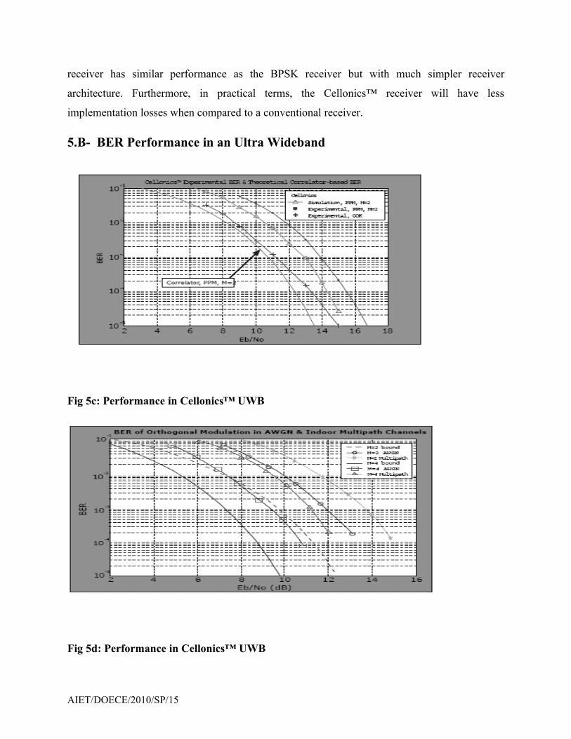
5.B- BER Performance in an Ultra Wideband
Fig 5c: Performance in Cellonics™ UWB
Fig 5d: Performance in Cellonics™ UWB
AIET/DOECE/2010/SP/15

UWB is a new radio system that occupies an ultra wide bandwidth. In UWB signaling, the
transmission uses very short impulses of radio energy (less than a few nanoseconds in duration).
This results in a spectrum that covers a wide range of radio frequencies. Consequently, the small
amount of transmitted energy is spread over a wide frequency range resulting in very small
energy per Hertz. It will cause little interference to the existing spectrum users. Typical
correlator-based UWB receiver requires thousands of cycles and frames to acquire the signals
and average out the noise.
The Cellonics™ technology can be used as a receiver to detect the UWB signals. The BER
performance of the Cellonics™ UWB system has been evaluated in both simulation and
experiment. Fig 4c shows the simulated and experimental results. Using the On-Off Keying
method, the experimental Cellonics™ performance curve is less than 1 dB from the theoretical
best performance using the correlate approach. However, the Cellonics™ UWB system has
superior throughput and is potentially hundreds to thousands times faster as it uses only one to
few frames (e.g. 7frames) to decode one information symbol depending on the power efficiency
requirements. Fig 4d shows its performance in a dense in-door multipath environment. The
fading margin is only3 dB and indicates that it is suitable for indoor applications such as wireless
local area networks.
AIET/DOECE/2010/SP/16
CHAPTER- 6
PROOF OF CONCEPT - DEMONSTRATION ON SYSTEMS
In the following discussions, the parameters used in the demonstration systems such as the
distance of transmission and the data rates are merely for ease of prototyping purposes and are
NOT the limitation of the Cellonics™ technology.
6.A- Narrowband Communication System
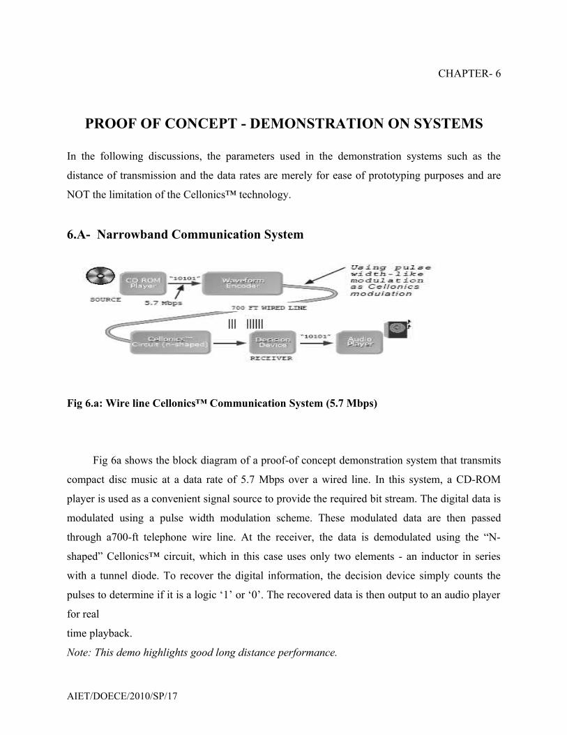
Fig 6.a: Wire line Cellonics™ Communication System (5.7 Mbps)
Fig 6a shows the block diagram of a proof-of concept demonstration system that transmits
compact disc music at a data rate of 5.7 Mbps over a wired line. In this system, a CD-ROM
player is used as a convenient signal source to provide the required bit stream. The digital data is
modulated using a pulse width modulation scheme. These modulated data are then passed
through a700-ft telephone wire line. At the receiver, the data is demodulated using the “N-
shaped” Cellonics™ circuit, which in this case uses only two elements - an inductor in series
with a tunnel diode. To recover the digital information, the decision device simply counts the
pulses to determine if it is a logic ‘1’ or ‘0’. The recovered data is then output to an audio player
for real
time playback.
Note: This demo highlights good long distance performance.
AIET/DOECE/2010/SP/17

6.B- Narrowband Communication System(Wireless)
Fig 6.b: Wireless Cellonics™ Communication System
Fig 6b shows the block diagram of another demonstration system which is a 26.7 Mbps file
transfer system. The system consists of a transmitter and receiver; both sub-systems further
comprise three modules: the PC/DSP module, baseband transceiver module and the RF
transmit/receive module. The DSP module resides in a personal computer and provides a high-
speed data transmission interface with the transmit/receive PC. The DSP transmits a data file
residing on the PC serially to the baseband transmitter at a data rate of 26.7 Mbps. The baseband
transmitter converts these data from the DSP into FSK-like waveforms. The RF receiver module
down converts the received signal using an AM envelope detector. The received waveform is fed
into the “S-shaped” Cellonics™ chip to recover the data. The recovered data are sent to the DSP
storage on the receiver PC. The transmission has no error correction scheme and the off-line
BER check has zero error most of the time. The demonstration system shows a high throughput
of data transfer and is 3 times faster as compared to a commercial Radio LAN product. Note:
This demo highlights better than current wireless LAN (11 Mbps) performance.
AIET/DOECE/2010/SP/18

6.C- Ultra Wideband Audio System
Fig 6c Cellonics™ UWB Wireless Audio Radio System
Fig 6c shows the block diagram of a UWB radio system. This system demonstrates the live
transmission of compact disc music using UWB wireless technology. Digital data from two CD-
ROM players is tapped at a rate of 11.4 Mbps. This data stream is fed into a UWB pulse
generator and transmitted wirelessly. At the receiver end, the signal is detected and then fed to a
Cellonics™ receiver to decode and the original music data is recovered/sent to an audio player
for real-time playback.
Note: This demo highlights future application and good noise immunity.
6.D- Ultra Wideband Video System
Fig 6d Cellonics™ UWB Wireless Video Radio System
Fig 6d shows the block diagram of a second UWB demonstration system that transmits real-time
video images at a data rate of 12Mbps wirelessly to a video monitor. In this system, a simple web
camera is used as the video capture source. The digital video information is fed into a pulse
position modulation processing board (a Field Programmable Gate Array or FPGA board) via a
AIET/DOECE/2010/SP/19

USB connection before being frequency translated to a higher frequency band at a transmitter for
sending over the air. The airborne signals are then detected by a UWB receiver and pulse
position demodulated back into digital video information for display at a video monitor. In both
instances, an ultra simple Cellonics Transmitter and a simple Celloncis receiver are used. The
speed of the system is only limited by the Video camera’s USB interface data rate.
Note: This demo highlights the ultra simplicity, speed and robust performance of the Cellonics
UWB transceiver technology in a popular consumer application.
AIET/DOECE/2010/SP/20

CHAPTER- 7
CELLONICS ADVANTAGES
The impact of Cellonics™ is such that it effects a fundamental change in the way digital
communications have traditionally been done. As such, many communication devices will
benefit from its incredible simplicity, speed and robustness.
Devices built with the Cellonics™ technology will save on chip/PCB real estate, power and
implementation time.
a. New Life to Communication Devices
The strength of the Cellonics™ technology lies in its inherent Carrier-rate Decoding™ (i.e.
extremely fast decoding rate), multilevel capability (spectral efficiency), simple circuitry, low
power consumption and low cost. Some telecommunication application examples in wireless
communication are cellular networks(2/3/4 G and beyond), W-LAN/Home networks ,LMDS,
broadcasting, military radio, RF identification tags, low cost radar with fine range precision and
sensor for automobiles. In wire line communication, some areas where the Cellonics™
technology is deployable are: high-speed modem cable modem, xDSL), LAN/Home networks,
backbone telephony/data networks, power line communications and military applications.
Beyond its application in telecommunication, the Cellonics ™ technology is also applicable in
the electronics circuits such as gated oscillators, delta modulators, sigma-delta modulators and
clock multipliers, etc.
b. Savings on Chip/ PCB Real Estate
Because of its simplicity, a receiver implemented with Cellonics™ can save as much as 4 times
the chip real estate. (Comparison made with a zero-IF receiver designed with the same 0.8Mm
BiCMOS process.)
AIET/DOECE/2010/SP/21

c. Savings on Power
Using the same design and comparison above, it was found that a Cellonics™-based receiver
consumed 3 times less power. This is possible because a Cellonics™ circuit is built with a few
discrete components that are mostly passive and hence consume very little or negligible power.
Cellonics™ returns a high 'power budget' back to a communication device. Designers can use
this 'extra' power to 'finance' other power-needy features in a device such a color screen, GPS
receiver, etc. Else, the device will simply end up having a longer battery life. (As in the case of
mobile phones.)
Table 7.a
d. Savings in Implementation Time
In a receiver, the Cellonics™ circuit replaces many traditional subsystems such as the amplifier,
mixer, PLL, oscillator, filter, crystal quartz, etc. that are necessary in a common Super
heterodyne and Super homodyne design. These parts in these subsystems can be costly, fragile
and noisy. Aside from this, the subsystems need great expertise to be put together and fine-tuned.
It is also difficult to miniaturize. With the simplicity and robustness of Cellonics™,
implementation time is swift without the sacrifice on performance.
e. Build or Rejuvenate your Products with Cellonics™
The incredible simplicity, low cost, low power consumption of Cellonics™ makes it ideal for use
in your next generation of feature-rich products that need to be small in size and long on power
reserve. Else, the technology is also ideal in giving your current products a new low- cost and
power-saving receiver engine.
AIET/DOECE/2010/SP/22
CHAPTER- 8
CONCLUSION
The Cellonics communication method is one inspired by how biological cells signal. It is
a fresh and novel look at how digital signals may be conveyed. In this digital day and age, it is
timely; current digital communication designs are mostly derived from old analog signal
methods. With the Cellonics method, much of the sub-systems in a traditional communication
system are not required. Noise-generating and power-consuming systems such as voltage-
controlled oscillators, PLLs, mixers, power amplifiers, etc., are eliminated. To a communications
engineer, this is unheard off. One just doesn’t build a communication device without an
oscillator, mixer, or….
Such is the revolutionary impact of Cellonics. Engineers will have to reform their
thinking- that such a simple solution is possible.
AIET/DOECE/2010/SP/23

REFERENCE
1: www.cellonics.com
2: www.future20hottechnologies.com
3: www.wikipedia.com/Cellonics technology
4: www.scribd.com
AIET/DOECE/2010/SP/24