intro to microcontrollers
TRANSCRIPT
HARDWARE FEATURES
CONTENTS AT A GLANCE
Different Types of MicrocontrollersEMBEDDED MICROCONTROLLERSEXTERNAL MEMORY MICROCONTROLLERSDIGITAL SIGNAL PROCESSORS
Processor ArchitecturesCISC VERSUS RISCHARVARD VERSUS PRINCETON
Microcontroller Memory TypesCONTROL STOREVARIABLE AREASTACKSHARDWARE INTERFACE REGISTERS (“I/O
SPACE”)EXTERNAL MEMORY
Device Packaging
Chip Technologies
PowerPOWER CONSUMPTIONCONNECTING POWER
Reset
System Clock/OscillatorsINSTRUCTION CYCLES
Program Counter
Arithmetic Logic Unit
2IN
TR
OD
UC
TIO
N
2

In the previous chapter, I introduced microcontrollers and talked a bit about architecturesand accessing programs, variables, and I/O. In this chapter I would like to discuss many ofthe more practical aspects of microcontrollers in terms of their internal features and intro-duce interfacing them to external devices.
If you’ve looked at the table of contents, you’ll probably feel like I explain every aspectof interfacing the microcontrollers. To be honest, I’ve only scratched the surface. Many dif-ferent devices use slightly different interfaces, different protocols, and interfaces that Ihaven’t even discussed here yet.
20 HARDWARE FEATURES
CONTENTS AT A GLANCE
Watch Dog Timers
Subroutines and Functions
Interrupts
Timers
Digital I/O
Level Conversion
Serial I/OASYNCHRONOUS SERIAL COMMUNICA-
TIONS
Synchronous Serial CommunicationsMICROWIRESPI
Network CommunicationsI2CCAN
Analog I/O
Slaved Devices
Device ProgrammingCONTROL STORE SECURITY
Debug Interfaces

Device PackagingWhen I use the term “device packaging,” I am describing the material (known as “encap-sulant”) that is used to protect the chip and the interconnect technology used to connect thechip electrically to the printed circuit card (which I call the “raw card”). There are quite afew options in this area, and selecting the appropriate ones to use can have a significantimpact on the final application’s cost, size, and quality.
There are two primary types of encapsulation used to protect chips: plastic and ceram-ic. Plastic encapsulants are the most prevalent and use an epoxy “potting compound” thatis injected around a chip after it has been wired to a “lead frame.”
The lead frame becomes the pins used on the package and is wired to the chip via verythin aluminum wires ultrasonically bonded to both the chip and the lead frame. Some chipsare attached to the lead frame using “C4” technology, which is described later.
Once the encapsulant has hardened, the chip is protected from light, moisture, andphysical damage from the outside world. EPROM microcontrollers come in a plasticpackage, and they are generally referred to as “one time programmable” (“OTP”) pack-ages. Once the EPROM has been programmed, the device cannot be loaded with anotherapplication. (Figure 2.1.)
The primary purpose of putting a microcontroller into a ceramic package is that aquartz window can be built into the package for the purpose of erasing the EPROM con-trol store. (Figure 2.2.)
When a ceramic package is used, the chip is glued to the bottom half and is wired to thelead frame. Ceramic packaging is typically only available as a PTH device, where plasticdevices can be a very wide range.
Ceramic packaging can drive up the cost of a single chip dramatically (as much as tentimes more than the price of a plastic OTP-packaged device). This makes this type of pack-aging only suitable for such uses as application debug, where the advantage of the windowfor erasing outweighs the extra cost of the package.
The technology used to attach the chip to the board has changed dramatically over thepast ten years. In the 1980s, pretty much all devices were only available in “pin throughhole” technology, in which the lead frame pins are soldered into holes in the raw card.(Figure 2.3.)
DEVICE PACKAGING 21
INT
RO
DU
CT
ION
2
Wire Bonds
Chip
Plastic Encapsulant
Lead Frame/Device Pins
Figure 2.1 OTP plastic package.

This type of attach technology has the advantage that they are very easy to work with(very little specialized knowledge or equipment is required to manufacture or reworkboards built with PTH chips). The disadvantages of PTH are the amount of space requiredto put the hole in the card, and requirements for space around each hole make the spacingbetween lead centres quite large in comparison to SMT technology, in which the pins aresoldered to the surface of the card. (Figure 2.4.)
There are two primary types of SMT leads used. (Figure 2.5.) The two different typesof packages offer advantages in certain situations. The “gull wing” package allows forhand assembly of parts and easier inspection of the solder joints. The “J” leaded partsreduce the size of the overall footprint. Right now, “gull wing” parts are significantly morepopular because this style of pin allows easier manufacturing and rework of very smallleads (with lead centres down to 0.016”).
The smaller size and lead centres of the SMT devices have resulted in significantlyhigher board densities (measured in chips per square inch) than PTH. Typical PTH lead
22 HARDWARE FEATURES
Chip
Window
Ceramic Package
Figure 2.2 Windowed ceramic package.
Solder
Hole or Via
Raw CardRaw Card
Figure 2.3 Pin through hole connection.

centres are 0.100” (with the minimum for “interstitial pins” being 0.071”), while SMTstarts at 0.050” and can go as low as 0.16”. The SMT parts with small lead centres areknown as “fine pitch” parts.
To give an idea of what this means in terms of board density, let’s look at a PTH pack-age that has pins at 0.100” lead centres and an SMT package with pins at 0.050” lead cen-tres. With the smaller lead sizes, the SMT package can be about half the size of the PTHpart in each dimension (which means that four SMT parts can be placed in the same spaceas one PTH part). As well, without holes through the card, components can be put on bothsides of the card meaning that in the raw card space required for one PTH part, up to eightSMT parts can be soldered to the card.
DEVICE PACKAGING 23
INT
RO
DU
CT
ION
2
Chip in PTH Package
Chip in SMT Package
0.100"0.050"
Lead Centres
"J" LeadedDevice
"Gull Wing"Leaded Device
Solder
Figure 2.4 PTH package size versus SMT.
Figure 2.5 Surface mount technology packages.
To both increase the board density and support chips with more pins, SMT pin lead cen-tres have shrunk to the point where 0.020” lead centre dimensions are not unusual. But, asthese pin counts go up, new packaging technologies have been invented to make boardassembly easier.
Assembly and rework of SMT parts is actually easier in a manufacturing setting thanPTH. Raw cards have a solder/flux mixture (called “solder paste”) put on the SMT padsand then run through an oven to melt the solder paste, soldering the parts to the board. Torework a component, hot air (or nitrogen gas) is flowed over the solder joints to melt thesolder, allowing the part to be pulled off. While SMT is easier to work with in a manufac-turing setting, it is a lot more difficult for the hobbyist or developers to work with (espe-cially if parts have to be pulled off a board to be reprogrammed).
For very high pin counts (300�) the PTH part is usually impractical because of its size,and SMT parts will have problems because of the difficulty in making sure all the pins stay“co-planar” (which is a fancy way of saying “undamaged” and all still bent the same way).For very high pin count devices, three technologies—”ball grid array” (“BGA”), “chip onboard (“COB”), and “tape automated bonding” (TAB)—are available.
In BGA technology, a two-dimensional array of solder balls is surface mounted to the chippackage and is then soldered to the raw card in the same way as an SMT part. (Figure 2.6.)
BGA offers some significant advantages over traditional SMT for very high pin countchips. Let’s take a 304-pin device, for example. Typically for SMT, this high a pin count ispackaged in an SMT package called a “quad flat pack” (“QFP”), which is a square pack-age with pins on all four sides with lead centres of 0.020”. A BGA package would consistof a 16-by-19 array of balls on 0.050” centres. The minimum SMT package size is 1.540”on each size (for 2.372 square inches), while the minimum BGA package size is 0.850” by1.000” (for 0.850 square inches). For this example, the BGA package takes up about a thirdof the space of the QFP and has an additional bonus that is not obvious. Because the ballcentres are 0.050”, it is much easier for the card assembler to place and solder onto a boardthan a component that has leads in the X and Y dimensions on 0.020 centres.
As noted before, the QFP pins would be very fragile (lead size for 0.020” lead centresis typically 0.012”, about twice the size of a human hair)) while the BGA part, having solidsolder balls, is a lot more robust. Because of the fragility of small SMT leads, manufac-turers typically try to place and solder these parts totally by machine without a human evertouching the parts. This level of concern is not necessary for BGA packages.
While placing and replacing a BGA part only requires the same tools as SMT parts, inspec-tion usually requires more sophisticated tools, including X-Ray machines. But BGA parts
24 HARDWARE FEATURES
Chip
Balls
SolderFigure 2.6 Ball grid array package.

have significantly higher quality than their SMT counterparts (an SMT part typically has a20–50-PPM lead defect rate, while a BGA can have as low as 1–2 PPM lead defect rate).
“Chip on board” (“COB”) packaging is very descriptive because in this type of pack-aging, a chip is literally placed on the raw card.
There are two methods of COB attachment that are currently in use. The first methodis to place the chip on the card and wire the pads of the chip to the pads on the card usingthe same technology as wiring a chip inside a package (using small aluminum wires ultra-sonically welded to the chip and raw card). (Figure 2.7.)
The chip itself can either be glued or soldered to the raw card. Soldering the chip to theraw card is used in applications where the raw card is to be used as a heat sink for the chip(which reduces the overall cost of the assembly).
The other method of COB is known as “C4” and is actually very similar to the BGAprocess described previously. The solder balls used in this process are called “bumps”(because they are so much smaller than BGA balls). (See Figure 2.8.) This technology wasoriginally developed by IBM for attaching chips to ceramic packages (without having togo through a wire bonding step).
The C4 attach requires a very significant investment in tools for placement and a veryspecialized process. (Because of the small distance between the chip and the card, waterused for washing the card can be trapped with flux residue, causing reliability problemslater.) C4 attachment is really in the experimental stage at this point, both because of thedifficulty in reliability in putting the chip down onto a raw card and the opportunity forfatigue failure in the bumps, caused by the chip and raw card expanding and contractingat a different rate due to heating and cooling.
DEVICE PACKAGING 25
INT
RO
DU
CT
ION
2
Chip
Wire Bonds
Plastic Encapsulant
Figure 2.7 Chip-on-board packaging.
Chip
Plastic Encapsulant
"Bumps"Figure 2.8 C4 chip-on-board packaging.

Chip-on-board packaging is best for very high volume applications, where a very shortspace is available for the chip (such as in telephone “smart cards”), or there are specialheatsinking requirements.
There is one last type of packaging that’s a combination of SMT and COB that’s called“TAB” (for “tape automated bonding”). In this type of packaging, the chip is bonded to acopper and kapton tape lead frame that is then soldered to the raw card. (Figure 2.9.)
TAB first came out in the mid-1980s as a method of providing very high pin counts forchips. With improvements in SMT packages (i.e., smaller lead centres) and the inventionof BGA, TAB has largely been made obsolete (although some chip manufacturers are stillworking with TAB). The problems with TAB centred around the need for specializedequipment for placing and soldering TAB components and the difficulty in inspecting thesolder joints.
When choosing a device package for an application, the choice you make can affect thesize of the finished product, its cost, the quality of the solder joints, and which card assem-bly sites can build and rework it.
I know I’ve thrown out a lot of information (and going with that, more TLAs (“ThreeLetter Acronyms”) than in any other part of the book. To be honest, I’ve just scratched thesurface in explaining all the issues regarding device packaging. When you are selecting thechip packaging for an application, please research all the options thoroughly and talk tothe engineers at the manufacturing site you are planning on using. (When it comes rightdown to it, they are the experts in their process and know what are the best packaging tech-nologies to use.)
Chip TechnologiesMicrocontrollers, like all other electronic products, are growing smaller, running faster,requiring less power, and are cheaper. This is primarily due to improvements in the manu-facturing processes and technologies used (and not the adoption of different computerarchitectures).
Virtually all microcontrollers built today use “CMOS” (“complementary metal oxidesemiconductor”) logic technology to provide the computing functions and electronic inter-faces. “CMOS” is a “push-pull” technology in which a “PMOS” and “NMOS” transistorare paired together. (Figure 2.10.)
Figure 2.10 is a diagram of a CMOS inverter or “NOT” gate. When the input signalis low, the PMOS transistor will be conducting (or “on”), and the NMOS transistor will
26 HARDWARE FEATURES
Chip
Solder
Tape C4 Bumps
Figure 2.9 Tape automated bonding package.

be “off.” This means that the “switch” (or transistor) at Vcc will be on, providing Vccat the signal out. If a high voltage is input to the gate, then the PMOS transistor will beturned off and the NMOS transistor will be turned on, pulling the output line to ground.
During a state transition, a very small amount of current will flow through the transis-tors. As the frequency of operation increases, current will flow more often in a given peri-od of time. (Put another way, the average current will be going up.) This increased currentflow will result in increased power consumption by the device. Therefore, a CMOS deviceshould be driven at the slowest possible speed, to minimize power consumption.
“Sleep” mode can dramatically reduce a microcontroller’s power consumption duringinactive periods because if no gates are switching, there is no current flow in the device.
An important point with all logic families is understanding the switching point of theinput signal. For CMOS devices, this is typically 1.4-volt to one-half of Vcc. But it can beat different levels for different devices. Before using any device, it is important to under-stand what the input threshold level is. (This will be discussed in greater detail below withregards of “level conversion.”)
CMOS can interface directly with most positive logic technologies, although you must becareful of low-voltage logic, to make sure that a “high” can be differentiated from a low inall circumstances (i.e., a “high” input is always above the voltage switching threshold level).
There are many more issues to be considered with different logic families, but I think Ihave brought up the major considerations. Each device is built with different technologies,so these issues are different for different devices.
Just to give you an idea of how microcontroller technology has improved over theyears, here is a comparison of two devices. The first is a mid-1980s vintage 8748,which is similar to the original IBM PC’s keyboard controller with the PIC 17C44, amodern PIC device. Both are 40-pin 0.600” devices, and both cost approximately thesame to buy.
CHIP TECHNOLOGIES 27
INT
RO
DU
CT
ION
2
Figure 2.10 CMOS NOT gate.
Vcc
NegativeSignal Out
SignalIn
PMOS Transistor
NMOS Transistor
Technology 8748H PIC17C44EPROM/Logic HMOS CMOSTechnologyEPROM Memory 2K 8KRAM Registers 128 Bytes 454 BytesMax Clock Speed 11 MHz 33 MHzCurrent Required 100 mA 38 mASleep Current Req’d N/A 1 uABuilt-in Functions 27 I/O Pins 33 I/O Pins
8-Bit Timer 3x 16-Bit TimersAsync/Synch I/O PWM I/O
Asynch/Synch I/O
PowerMany microcontroller applications are powered by batteries and may even rely on “super-capacitors” for staying operational during power outages. For this reason, minimizingpower consumption in microcontrollers is an important issue.
As noted above, virtually all microcontrollers today are built using CMOS technology,which requires significantly less power than older, bipolar or NMOS-based devices. Butthere are some considerations in ensuring that the application only uses as much power asit requires.
Because of the wide variety of different applications and power sources microcon-trollers are designed for, their power-handling circuitry is often designed as robustly aspossible to ensure that the device will run under a variety of conditions.
One important point to note on power is all the different terms that can be used todescribe it. For different devices, you’ll see “Vcc” and “Vdd” to indicate power (typically�5 volts, although in some devices it can be as low as �2 volts). Similarly, “Vss” and“Gnd” is used to indicate Ground. In this book, I will use “Vcc” to indicate power (evenwhen the manufacturer uses “Vdd”) and “Gnd” to indicate ground.
POWER CONSUMPTIONThere are three conditions that have to be considered when planning for a microcontroller’spower consumption in an application. The first is what I call “intrinsic power,” which is thepower required just to run the microcontroller. Next, there is the “I/O drive power,” whichtakes into account the power consumed when the microcontroller is sinking/sourcing cur-rent to external I/O devices. The third is the power consumed when the microcontroller isin “sleep” or “standby” mode and is waiting with clocks on or off for a specific externalevent. Taking these three conditions into account when planning an application can changean application that will only run for a few hours to literally several months.
“Intrinsic power” is the power consumed by the microcontroller when it is runningand nothing is connected to the I/O pins. This consumption of power is largely a func-tion of the CMOS switching current, which in itself is a function of the speed of themicrocontroller.
28 HARDWARE FEATURES

By decreasing the system clock frequency, the intrinsic power can be reduced signifi-cantly. For example, the chart below shows the current requirements (“Idd”) for aPICMicro 16C73A running at different frequencies with 5 volts power input.
FREQUENCY CURRENT
1.0 MHz 550 uA2.0 MHz 750 uA3.0 MHz 1 mA4.0 MHz 1.25 mA
By lowering the clock speed used in an application, the power required (which is sim-ply the product of input voltage and current) will be reduced. This may mean that the appli-cation software may have to be written “tighter,” but the gains in product life for a givenset of batteries may be an important advantage for the application.
Obviously, the intrinsic power consumption can be further reduced by supplying a lowervoltage input to the microcontroller (which may or may not be possible, depending on thecircuitry attached to the microcontroller and the microcontroller itself). Many devices aredesigned to run on as little as 2.0 volts.
The I/O drive power is a measurement of how much power is sourced/sunk by themicrocontroller to external devices and is unique to the application. In many applications,the microcontroller is the only active device in the circuit (i.e., it is getting input fromswitches and outputting information via LEDs). If the microcontroller is driving devicescontinually at times when they are not required, more current (which means more power)than is absolutely necessary is being consumed by the application.
The last aspect of power consumption to consider when developing an application is“sleep”/”standby” mode. This is usually entered by executing a special instruction andafter executing this instruction, the microcontroller shuts down its oscillator and waits forsome event to happen (such as a watchdog timer to count down or an input to change state).
Using this mode can reduce the power consumption of a microcontroller from milli-watts to microwatts. An excellent example of what this means is taken from the ParallaxBASIC Stamp manual in a question-and-answer section:
How long can the BASIC Stamp run on a 9-volt battery?
This depends on what you’re doing with the BASIC Stamp. If your program never uses sleep modeand has several LEDs connected to I/O lines, then the BASIC Stamp may only run for severalhours. If, however, sleep mode is used and I/O current draw is minimal, then the BASIC Stampcan run for weeks.
Using the sleep mode in a microcontroller will allow the use of a virtual “on/off ”switch that is connected directly to the microcontroller. This provides several advan-tages. The first is cost and reliability; a simple momentary on/off switch is much cheap-er and much less prone to failure than a slide or toggle switch. Second is operational;while sleep mode is active, the contents of the variable RAM will not be lost or changed.And the last advantage is purely aesthetic; I like applications that use a push-buttonswitch for on/off.
POWER 29
INT
RO
DU
CT
ION
2

There is one potential disadvantage of sleep mode for some applications, and that is thetime required for the microcontroller to “wake up” and restart its oscillator. This can be aslong as ten milliseconds, which will be too long for many applications. Actually, I wouldprobably qualify it to say that it’s probably too slow for interfacing with other computerequipment. If the main thing the microcontroller is interfacing to is a human, this wake-uptime will not be an issue at all.
One thing to remember with sleep mode is to make sure there is no current draw whenit is active. A microcontroller sinking current from an LED connected to the power railwhile in sleep mode will result in extra power being consumed.
CONNECTING POWERA microcontroller is often put into applications in which its power may be less than opti-mal. Application power sources can include radio battery power, rectified and roughly fil-tered AC, or generator output. This means that microcontrollers will run with a variety ofvoltage inputs and interface to devices running at different logic levels. Microcontrollersare designed to run in environments that can be described as inhospitable and impossiblefor many other electronic devices.
Fortunately, most microcontrollers will take these variances in stride and work withoutcomplaint. The only issue to be considered when doing a microcontroller application is thedecoupling of the power voltage. Typically, I use a 0.1-uF tantalum capacitor as physical-ly close as possible to the Vcc (or “Vdd”) input pin. This will allow the device to handlemuch greater I/O current transients without causing inadvertent resets or data corruption.This simple capacitor will hide a multitude of sins.
ResetEnsuring that a microcontroller runs only during valid environmental conditions is usally crit-ically important to an application. Looking back over what I’ve written here, it is very appar-ent that reset can only take place when you are sure power to the microcontroller is valid.
Typically, microcontroller applications begin to operate when power is applied to thedevice. To ensure that power has stabilized, I like to use the circuit shown in Figure 2.11.
With this circuit, reset becomes active approximately 22 msecs (using the approxima-tion of the time delay � 2.2 RC) after power comes up. This gives lots of time for powerand the device’s oscillator to stabilize before the microcontroller begins operation.
The “momentary on push button” (“manual reset”) is used to allow resetting the applica-tion during application development. When you are debugging an application, you will findthat it is useful to control reset and be able to restart the microcontroller (to help characterizea problem). The 100-ohm resistor in series with the capacitor will limit current from the capac-itor during reset (a charged capacitor will behave like a high current source when shorted toground). This circuit can be used with microcontrollers which have a positive active reset(such as the 8051) by inverting the voltage at the capacitor (using something like a 7404).
In some microcontrollers, the RC network can be deleted because of internal circuitrywithin the device that puts in a delay before allowing the microcontroller to become active(i.e., start the oscillator and begin to execute the instruction at the reset address).
30 HARDWARE FEATURES

This means the circuit can be simplified to what is shown in Figure 2.12. Looking atthis, you are probably thinking that the circuit can be further simplified to just a connec-tion between the reset pin and Vcc. This is true, but should only be done when the circuitis complete and debugged (and even then, I would like to see a current-limiting resistor putin place to allow resetting of the device by shorting reset to ground).
These reset circuits are best used in applications where the power voltage (Vcc) can beguaranteed to be within operating limits. Many microcontroller applications rely on bat-teries, which produce lower voltage over time. As the voltage drops, this may make theapplication run erratically, as some devices’ cut-off voltage is reached before others.
To eliminate this as a problem, there are devices (known as “brown-Out” circuits)designed to monitor the Vcc/Vdd level and if it drops below a predetermined point (usu-ally 4.5 volts), reset will be asserted actively. Typically, these voltage-monitoring circuitsinclude a delay to operate similarly to the RC reset circuit above and monitor the incom-ing voltage level and are packaged similarly to a three-leaded transistor.
RESET 31
INT
RO
DU
CT
ION
2
Vcc
MCUReset
10K
100 Ohm
0.1 uF
ManualReset
Figure 2.11 Full reset circuit.

System Clock/OscillatorsIf you’ve worked with designing clock circuits for microprocessors, you will find yourselfin a pleasant surprise when designing the clock circuitry for a microcontroller circuit.Microcontrollers are designed for requiring the minimum amount of external circuitry fortheir system clocks.
Most microcontrollers are designed to be able to run at a very wide range of frequencies:from literally DC (no clock transistions at all) to tens of megahertz. This is accomplished bythe use of fully static logic and memory designs internal to the microcontrollers. While I havenot done this personally, I have known of people who have run applications at 1 Hz or less tosingle-step through their designs to debug the software. This extreme frequency range allowsthe application designer to better tailor the microcontroller appropriately to the application.
There are three different methods used for providing a clock in a microcontroller, andeach has unique advantages and disadvantages. The first method of providing a clock to amicrocontroller is by using a crystal, wired as shown in Figure 2.13.
32 HARDWARE FEATURES
Figure 2.12 Modified reset circuit.
Vcc
MCUReset
10K
ManualReset

This allows a crystal with a very precisely specified frequency (typically with an error rateof 100s of parts per million) to be used to drive the microcontroller. This level of precisionis required for interfacing with other devices (or ensuring that a real-time clock is accurate).
The values of the capacitors used are specified by the microcontroller manufacturer fora specific crystal frequency. Sometimes a very large (on the order of megohms) resistoracross Clk0 and Clk1 is required for the clock to run stably. Often, a manufacturer willspecify that a variable capacitor is attached to Clk1 to allow the oscillator to be “tuned” tothe exact frequency.
I, personally, hate to have any tunable parts in any application that I design, and I havenever designed a microcontroller clock circuit that required a tunable part. If frequency tol-erance is a problem, I will use another clocking circuit that won’t have this problem.
As a rule of thumb, less capacitance will give you a better waveform. If you put oncapacitances that are too large, your clock will degrade to the point where the microcon-troller won’t start up. If you aren’t sure about the capacitance values you are using, take alook at the clock waveforms using a high-impedance probe with an oscilloscope. Youshould see the upper waveform shown in Figure 2.14.
If you have overloaded your circuit with too much capacitance, you will see somethinglike the lower waveform, if the microcontroller runs at all (if it doesn’t, the signal will bea DC voltage at approximately Vdd/2).
The two major disadvantages of this clocking method are the number of componentsthat are required and the fragility of quartz crystals. Both of these problems can be elimi-nated by using a ceramic resonator. A ceramic resonator is much more resistant to physi-cal shocks, and many are available with built-in capacitors, reducing the parts count fromthree devices to one. Ceramic resonators typically have a frequency accuracy of severalthousand PPM (roughly 0.5%).
SYSTEM CLOCK/OSCILLATORS 33
INT
RO
DU
CT
ION
2
CrystalExt.Caps
Mic
roco
ntro
ller
Clk0
Clk1
Figure 2.13 Crystal-based microcontroller clock.
The next type of system clock is the “RC oscillator.” This method of clocking uses thecharacteristic rise/fall time of an RC network to provide a repeatable delay as a clock.(Figure 2.15.)
This is the cheapest method of providing a clock to a microcontroller—unfortunately,it’s also the least accurate. Whereas a crystal provides an error of only tens of PPM, and aceramic resonator in the thousands of PPM, the RC network is only accurate to hundredsof thousands of PPM.
In some limited experimentation with the PIC, I have found that the accuracy of an RCoscillator is up to 20% (or 200,000 PPM). While this is obviously unacceptable for manyapplications where timing is critical, this may not be an issue for other applications.
There is no general formula for calculating the resistor or capacitor values for this typeof oscillator. This is because of the internal parts of the microcontroller which nonlinearlysink current. Values for R and C to oscillate at an approximate frequency can be found inthe microcontroller’s data sheets.
The great advantage of this method is the low cost of this solution; the external cir-cuitry for an RC oscillator can be less than one cent! Looking at the circuit, you areprobably feeling that it can be tuned to a precise frequency by using a variable resistoror capacitor. Yes, this is true, but the complexity (and the cost) of the oscillator schemeis increased.
Another type of oscillator isn’t one at all; it’s bringing in an external clock signal. As Ihave said, microcontrollers are capable of running at an extremely wide range of frequen-cies. An external clock can be almost literally any frequency possible.
Some microcontrollers have internal RC or “ring” oscillators which can be used to runthe device without any external parts for the oscillators. The internal oscillators are usual-ly enabled by a configuration register that is programmed with the control store.
34 HARDWARE FEATURES
GoodClock(Approx.SquareWave)
PoorClock(FlattenedSine Wave)Too MuchExternalCapacitanceFigure 2.14 Good and bad PICMicro clock waveforms.

INSTRUCTION CYCLESIf you are new to processors in general and microcontrollers specifically, one thing thatyou will be surprised to find out is that an instruction cycle is not the same as a clock cycle.An “instruction cycle” is usually defined as the number of clock cycles that are requiredby the processor to do a useful piece of work. In Figure 2.16, the instruction cycle is fourclock cycles long.
The instruction cycle is usually executed within the processor/microcontroller as a min-imal operation, using the clock cycles to provide timing for each event within the instruc-tion cycle.
Some instructions in all microcontrollers take more than one instruction cycle to exe-cute. This can make timing operations within the microcontroller difficult and often a man-ual exercise with a data book or using a simulator/debugger to time program execution. Inthe example applications chapters later in this book, I show some of the practical aspectsof setting up precise timing loops.
SYSTEM CLOCK/OSCILLATORS 35
INT
RO
DU
CT
ION
2
Mic
roco
ntro
ller
Clk0
Clk1 N/C
R
C
Figure 2.15 RC network microcontroller clock.

Program CounterThe program counter (“PC”) is used to keep track of where the program is currently exe-cuting. This function is made more complex by having to save the current value duringinterrupts and subroutine calls as well as just simply to branching to a new location. Figure2.17, while showing some of the complexity of the PC, really doesn’t show all the differ-ent things that the program counter is responsible for.
The PC is really a parallel input/output counter. The diagram shows how a programcounter would be implemented in a Princeton-architected machine. In this type of proces-sor, the value of the PC is read and sent through the data bus to the memory controller toprovide an address to read (often the program counter will be part of the memory controllerto eliminate the overhead of passing the current address through the data bus). The impor-tant features of the counter are the parallel load (which updates the program counter fromthe data bus), the reset (which resets the PC to reset address of the microcontroller), andthe increment (or clock) line (which is toggled after each instruction is read in). These linesare controlled by the instruction decode unit, which sequences how the microcontrollerexecutes.
The “parallel load” option is used to load in “goto” (or “jump”) or “call” (subroutine)addresses. In Princeton-architected machines, this address has to come through the databus. While I describe these devices as having 8-bit processors, they’re usually a hybridbecause the program counter is usually larger than 8 bits (which would only allow address-ing 256 memory locations). When the address is being updated, the new address has tocome through the data bus 8 bits at a time (which takes extra cycles). To reduce this addressload overhead, some processors have “branch” instructions in which only the least 8 bitsof the new address are loaded into the program counter (the other, more significant bits areleft unchanged). Executing a “branch” instruction means that only one byte has to beloaded through the data bus as opposed to at least two for the full “jump” instruction if a16-bit address space is provided.
36 HARDWARE FEATURES
InstructionCycle
ClockCycle
1x Instruction CycleFigure 2.16 Instruction cycle versus clock cycle.

The reset value for the microcontroller’s processor can be any value. While beginningexecution at address 0x000 might seem to be the most obvious value, different microcon-trollers will begin execution at different addresses. There is also a similar value (or “vec-tor”) for interrupts. Interrupts usually load the PC with a specific value which is differentfrom the reset address, but may use the same hardware.
After each instruction is read in, the program counter is incremented. This is done tomake sure it is loaded with the next address, so if a subroutine call or an interrupt is exe-cuted, the return address (which is the next instruction) can be saved on the stack, withouthaving to execute additional cycles to increment the program counter.
There are some important things to note about the increment function of the programcounter. In Princeton-architected microcontrollers, care must be taken in the software tomake sure the program counter doesn’t leave the program area (i.e., increment outside ofit). If this happens, you can literally be executing data (which obviously will have unpre-dictable results) as the PC strays outside of the control store area.
Another issue to consider is, what happens when the program counter reaches the end ofthe memory space? In some devices, it wraps around to address 0x000, but in others it con-tinues to increment with the instruction decode circuitry, executing indeterminate instructions.
Arithmetic Logic UnitThe arithmetic logic unit (“ALU”) of a processor is used to carry out all the mathematicaloperations of a program. These operations include addition, subtraction, ANDing, ORing,
ARITHMETIC LOGIC UNIT 37
INT
RO
DU
CT
ION
2
Parallel Load CounterIncrement
ResetParallel Load
FromDataBus
To Control Store
To DataBus
Figure 2.17 Program counter.

shifting registers and values, and passing the status of these operations to the status Register.The ALU is not used to read or save data or instructions, nor is it used to execute instructions.
The ALU is probably best presented as hardware that combines two words of data andstores the result. (See Figure 2.18.) How this data is brought in and stored is a major con-sideration of different microcontrollers (and is one of the major differenciators betweenprocessors and instruction sets). Some designs will take source from an accumulator(along with another word) and put the result back in the accumulator. Others will allow youto specify the two different sources and the destination.
ALUs typically only work with positive integers. However, “twos complement” nega-tive numbers are usually produced as a matter of course when a number is subtracted froma smaller number. This can lead to some confusion with how the ALU works and what kindof result is to be expected.
In the Microchip PIC, this can be shown in how the subtraction instructions work.Instead of actually subtracting one number from another, it actually adds the negative.You’re probably thinking to yourself, what difference does this make? In grade school, youwere probably taught that:
A - B � A � ( � B )
In binary systems, the equation above is actually not true. It makes a lot of differencewhether you are subtracting or adding the negative. To get the twos complement negativeof a number, it is complemented and then incremented:
� B � ( B ^ 0x0FF ) � 1
By providing circuitry to do this negation, a subtractor doesn’t have to be designed intoan ALU, just an Adder. Through substitution:
A � B � A � ( B ^ 0x0FF ) � 1
This method of handling a subtraction can be confusing when the carry flag is used for bothaddition and subtraction. In “typical” ALUs (which have an adder and subtractor) the carry bitis often referred to as a “carry/borrow” flag. In this case, the bit is set when the result of addi-tion is greater than 0x0FF or the result of subtraction is less than zero. In both cases, the bit is
38 HARDWARE FEATURES
Status BitsALU
Dest
Src1 Src2
Figure 2.18 Arithmetic logic unit block diagram.

used to indicate when upper 8 bits of the number are affected by the operations on the lower8 bits. In the case where the ALU doesn’t have a subtractor (as in the example above), the carryflag is still checked after addition or subtraction, but it works differently.
To understand what happens, let’s go through a couple of examples. The first exampleis to show what happens when a number is subtracted from a value larger than itself (result-ing in a positive number):
0x077 � 0x055 � 0x077 � ( � 0x055 )
� 0x077 � ( 0x055 ^ 0x0FF ) � 1
� 0x077 � 0x0AA � 1
� 0x0125
The result is greater than 0x0FF, which causes the carry flag to be set (which is notexpected in the case of a carry/borrow flag). The least significant 8 bits are 0x022, whichis what will be transferred to the destination, which is the answer that we expect.
Next, consider the case where a number is subtracted from a smaller one, which resultsin a negative result:
0x055 � 0x077 � 0x055 � ( � 0x077 )
� 0x055 � ( 0x077 ^ 0xOFF ) � 1
� 0x055 � 0x088 � 1
� 0x0DE
In this case, in a “normal” ALU, we would expect the result 0x0DE and the carry/bor-row flag to be set. Again, the least significant 8 bits are as expected and the most signifi-cant bit (which will be loaded into the carry flag) is not.
Trying to understand this situation, you can see that the carry flag is set when the sub-traction result is positive and reset when the result is negative. In this situation, I think ofthe carry flag as the “carry/positive” flag. After going through these examples, you can seethat this actually is quite easy to understand, but when you first see the operation of theinstructions and the status flag results, it’s easy to become confused and unable to under-stand exactly what is happening.
One last thing to consider with ALUs is that when you look at a family of devices, somehave features which you would expect in the ALU (multiplication is a classic example ofthis). It would be wrong to assume that the ALU is different between the different mem-bers of the family.
Instead, the extra function is probably added as extra hardware to the silicon-likeenhanced peripheral functions and doesn’t affect the ALU at all. This means that the newfeatures use registers that are unrelated to the ALU status register and accumulator(s). Forexample, looking through different members of the Motorola 6800-based microcontrollerfamily, I found this to be the case.
After reading this section, you’ll probably realize that the ALU is as complicated as themicrocontroller as a whole. Often, manufacturers have whole teams working on the ALUthat are equal in size to the teams that are designing the rest of the microprocessor ormicrocontroller (probably more when something like a PC processor is being designed).How the ALU works affects the operation of the processor within the microcontroller, andthe operation of the microcontroller as well.
ARITHMETIC LOGIC UNIT 39
INT
RO
DU
CT
ION
2
Watch Dog TimersOften in electrically “noisy” environments, induced signals and currents will cause amicrocontroller to jump to an unexpected memory location unexpectedly and run in anunexpected manner (this is usually referred to as the microcontroller “running amok” orhas taken a “branch to the boonies”). To monitor this, an aptly named device called the“watch dog timer” is often implemented in the silicon of the microcontroller.
This device causes a reset of the microcontroller if it is not updated within a predeter-mined amount of time (usually tens of milliseconds to several seconds). If a microcontroller’sinstruction pointer is inadvertently changed, then chances are, it will not re-acquire the watchdog timer update code and be reset by the watch dog timer and placed back in a known state.
I, personally, have never enabled a watch dog timer in an application. This is because Ihave never felt that it has been required from the electrical “noise” point of view (i.e.,putting a microcontroller in a CRT display, close to the flyback transformer or close to anautomobile’s ignition coil). This may sound a bit facetious, but I feel that with modernelectronics, the chance of an electrical upset is remote—although it would be very real insituations similar to the ones above.
I would also recommend against using the watch dog timer for masking software prob-lems. While this may reduce the chances that the code will cause something bad to hap-pen, I don’t feel that it will eliminate all possible instances of this, and rather than relyingon the hardware to prevent software-induced upsets, testing of the software under all situ-ations should be carried out.
Subroutines and FunctionsI realize that typically subroutines and functions are discussed in many books and coursesas programming constructs and techniques. What I wanted to do here is discuss the hard-ware used to implement the calling subroutines and passing parameters back and forth.
Calling a subroutine involves saving the current program counter so that the “return”operation knows where to restore the program counter. This can be accomplished by auto-matically (as part of the “call” instruction) pushing the return address onto a “programcounter stack,” then when a “return” instruction is executed, this address is popped off thestack and put into the program counter.
But what about devices that don’t have stacks? One example that will probably surpriseyou is the IBM 370 mainframe architecture; it doesn’t have a stack for storing the programcounter or any register contents. In these types of architectures, a return value is stored ina register any time a “goto” is executed. This leaves it up to the software developer to deter-mine what is the most efficient way to save the return address. The best way of imple-menting a “call” may be simply leaving the return address in the register if the subroutinedoesn’t call any “nested” routines (and then to return from the subroutine, putting the con-tents of the register into the program counter).
Along with stacks, saving the return address following a goto instruction in a registermay not even be available in some devices. So to implement a subroutine call, the returnaddress has to be saved in a variable.
40 HARDWARE FEATURES

This could be implemented by the code:
.:ReturnVar = AfterGoto ; Save the Return Addressgoto Subroutine ; “Call” the Subroutine
AfterGoto.:
Subroutine ; Start of the Subroutine.:ProgramCounter = ReturnVar ; Return to Instruction AFTER goto
Complicating subroutines are functions. I define a function as a subroutine with para-meters passed to it and returned from it. For example, a “C” function could be declared as:
int Func( int i, char far * Ptr );
In this example, “Func” is defined as a function that requires two input parameters, aninteger and a pointer, and returns an integer. One of the most efficient (and most-often imple-mented) methods of passing parameters to a function is to put them on the (program counter)stack before the subroutine/function is called. Once in the subroutine, the index register canbe given the current stack value and can reference these values. This method of handlingparameters has one significant advantage over other methods and that is the memory usedfor storing the parameters is completely resuable. Variables declared within a function (andthis includes the input parameters) are often called “local” or “automatic” because they areonly usable locally in the function, and the space for them is created automatically.
While it appears that this type of function calling can only be accomplished by havinga stack built into the processor, it can be accomplished by using an index register to sim-ulate a stack. If a program counter stack is not available for pushing data, the simulatedstack can also be used to store the return address of the calling routine.
The other methods of passing parameters are putting the input parameters into theprocessor’s registers or into special variables. While passing input parameters in processorregisters is possible in some cases, it will cut down on the number of registers available inthe function. Storing input parameters in special variables is also possible but reduces theamount of memory available in the program (and memory is often at a premium in amicrocontroller).
Returning a parameter can be done in any of the three ways discussed for passing para-meters into the function. But the returned value is typically returned in the processor’s reg-isters because this is the most efficient (fastest) method of transferring the data, and reg-ister space is available.
InterruptsFor most people, interrupts are in the class of hardware best left alone because it requiresgodlike knowledge of the processor to develop interrupt handler code for an application(lest the system freezes up or runs amok when an interrupt is encountered). This feelingusually comes from experiences trying to program interrupts for the PC. The PC has manyissues which complicate the development of an interrupt handler that are not relevant in a
INTERRUPTS 41
INT
RO
DU
CT
ION
2

microcontroller environment. Actually, using interrupts in a microcontroller environmentcan simplify applications and make their development easier.
If you’ve never been exposed to interrupts, you may wonder exactly what they are. In acomputer system, an interrupt is a special subroutine (called an “interrupt handler” or“interrupt service routine”) that is requested by a hardware event, to be executed after sus-pending the execution of the currently running program. The term “interrupt request” isused because sometimes the software will refuse to acknowledge the interrupt and executethe interrupt handler immediately. (Figure 2.19.)
Interrupts in a computer system are exactly analogous to interrupts that you mayencounter in your everyday life. The classic example of real-life interrupts (at least for me)is what happens when the phone rings while you are watching TV.
When the phone rings, you have three possible responses. The first is to ignore thephone and let the answering machine take a message that you’ll deal with after the showis finished. The second response is to answer the phone, but take a message and say you’llcall back later. The last possible response is to record the remainder of the show on yourVCR while you take the call and then watch the taped show when the call is complete.
In a computer system, there are three similar responses that can be used to respond tothe external hardware event. The first possible response (not responding to the interrupt atall until the current task is complete) could be accomplished by disabling (or “masking”)the interrupt sources and when the task is complete, either “unmasking” the interruptsources (which causes the interrupt handler to be executed and the event will be handled)or by looking at (also known as “polling”) the interrupt request bits and executing theresponse code directly, without having to deal with the interrupt handler. This method ofhandling interrupts is used when the mainline code is critically timed and any interruptionscan cause it to fail to interface properly.
42 HARDWARE FEATURES
MainlineCodeExecution
InterruptHandler
Sav
e R
egs
Rst
Int
H/W
HandleInt
Res
tore
Reg
sR
etur
n
Figure 2.19 Interrupt execution flow.
Masking interrupts for long periods of time is not recommended because of the dangerof having multiple events lumped together and only being recognized as one. Defining“long periods of time” is dependent on the application and the type and frequency ofevents and the interrupt. As a rule of thumb, interrupts should not be masked for more thanhalf of the shortest period between the expected period between interrupt requestingevents.
An interrupt handler always takes the form:
1. Save the “context registers.”2. Reset the interrupt controller hardware and reset the requesting hardware.3. Handle the data from the interrupt.4. Restore the “context registers.”5. Return to the previously executing code.
The “context registers” are the registers used to determine the current execution state ofthe mainline code. Typically, these registers are: the program counter, the status registers,and accumulator(s). Other processor registers, such as the index registers, may be used inthe interrupt handler, so these should be saved at this time as well. These other registersare device and application specific.
Next, the processor’s interrupt controller is reset, ready to accept another interrupt, andthe hardware that generated the interrupt is reset, also ready to accept again the condi-tions which caused the original interrupt. I like to do this at this point because anotherinterrupt request may be received by the interrupt controller. If everything is reset andready for another interrupt, the processor’s interrupt mask register will prevent the inter-rupt request from being handled, but the interrupt status register will record the event sopending interrupt requests can be handled when the current interrupt has completed andinterrupts are unmasked.
Nested interrupts may not be easily implemented in some microcontrollers (thesedevices typically don’t have a data stack) or may cause potential stack overflow problems.The issue of the stack overflowing is a concern in microcontrollers because of their limit-ed RAM and stack; allowing nested interrupts may cause more data to be put on the stackthan was expected or available.
Finally, the interrupt is processed. In the second TV example, the interrupt was handledas quickly as possible and then the data received was used to carry out the requested task.In a microcontroller, this would be the same as putting the incoming data on an array andthen dealing with it when the primary task has been completed. This is a good compromisebetween fully handling the interrupt (which may take a long time) and ignoring it (whichmay result in events being lost).
Restoring the context registers and executing the interrupt return instruction puts theprocessor back in the exact state it was in when the interrupt handler was invoked.
You may be wondering what happens to the various registers during interrupts. I havediscussed a number of things that happen, but I thought it would be a good idea to sum-marize what actually happens. The status register is often saved along with the programcounter when an interrupt begins executing. This eliminates the effort required to move itto and from the area used to save it without changing it before returning to the previouslyexecuting code. This does not happen in all architectures, so care must be taken when han-dling interrupts (this will be shown in the application section of each microcontroller). If
INTERRUPTS 43
INT
RO
DU
CT
ION
2

the status register is saved at the start of interrupt execution, the interrupt return instruc-tion will restore it as well.
If other registers within the processor are changed within the interrupt handler, thesetoo should be saved before they are changed and restored before returning to the mainline.I find that I typically save all the processor’s registers, with the feeling that it’s better safethan sorry (and sorry in this case will probably be debugging a microcontroller workingunpredictably at difficult-to-reproduce intervals or circumstances).
The address that the program counter jumps to on acceptance of an interrupt requestis known as a “vector.” (There are several types of vectors; the address the programcounter is set to after reset is called the “reset vector.”) There may be multiple vectors fordifferent interrupts, which eliminates the code required for determining which interruptcaused the handler to execute. Different interrupts sharing the same vector are usually nota serious problem in microcontrollers because the application is the only program runningin the processor. This is different from the PC, where multiple interrupt sources can beadded at different times. (If you’ve ever set up two devices on the COM1 and COM3ports, you’ll know exactly what I am talking about.) In a microcontroller application,where the hardware is well known, there shouldn’t be any problems if interrupt vectorsare shared.
The last point I want to make about interrupts is the use of “software interrupts.” Theseare processor instructions that can be used to simulate a hardware interrupt. The most obvi-ous use for these instructions is to “call” system subroutines that have arbitrary locationsin memory or require “long calls” to access. This feature is built into the Intel i86 and isused in the IBM PC’s BIOS (basic input/output system) and PC-DOS to provide systemsubroutines without having to place entry points at specific locations in memory. Instead,the different interrupt vectors point to the code to be executed when the interrupt is“called” in software.
After reading this section, I don’t know if interrupts will seem easier to you or if I’vescared you away from them even more. As I introduce each microcontroller, I will showhow interrupts are implemented and how they can simplify an application.
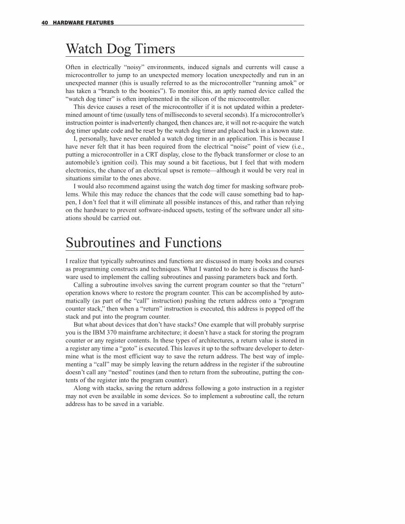
TimersIf you’re familiar with microprocessors, you’ll probably think that they are only used forproviding a constant delay. In microcontrollers, timers are used for a lot more applications.
Being used as a straight timer usually involves setting the timer to use the instructionclock as an input (as opposed to an external signal). By loading in an initial count, a spe-cific time interval can be timed, the overflow indicating when the interval has beenreached.
Often, a “prescaler” is put in front of the timer to allow longer intervals to be measured.This hardware will only allow the timer itself to be incremented when a specific count isreached. (Figure 2.20.)
If you wanted to get a 10-msec (1/100 sec) delay in a system that had a 10-MHz clock,you could use the circuit shown in Figure 2.20 in the following manner.
First, a prescaler value would have to be determined. At 10 MHz, this means the timerwould have to count 10,000 times, which is impossible for an 8-bit counter.
44 HARDWARE FEATURES
So a prescaler value has to be chosen to get a good count value. Typically, a prescalervalue is simply a power of two (i.e., 1, 2, 4, 8,...256). If a prescaler value of 64 is chosen,that means the timer has to count to 156 (64 � 156 � 9,984, which is a close approxima-tion and can be nailed down exactly by adding “nop”s or other time-wasting instructions).
Now, to wait for this interval, the timer could be cleared and the value in the timer con-tinually compared against 156. Or a more efficient way is to load the timer with 256-156and wait for the timer overflow interrupt flag to be set.
With the latter method, a simple multitasking program could be written, with a taskswitch taking place when the timer counts down the 10-msec delay.
While this method can be used to provide a real-time clock function for a microcontroller,it is not recommended. Often, when a timer is reloaded, the prescaler is at an unknown value(and is not deterministic) and is reset when a value is put into the timer registers. Instead, let-ting the timer run continuously is best (the prescaler is never reset), and when the timer over-flow is indicated, the bit is simply reset and a real-time clock counter is incremented. Thismeans that when the program wants to know the current time, it simply takes the real-timeclock counter value and manipulates it to get the correct time. This is the method used by theIBM PC and is the reason why each real-time clock “tick” occurs 18.2 times per second.
With the circuit above, you can see that the clock can also be used to count events exter-nal to the microcontroller. This is accomplished by simply selecting the Timer input sourcefrom “Instruction Clock” to “External Clock” in the circuit above.
If the microcontroller had two timers, a simple tachometer (event per unit time counter)could be easily created. (Figure 2.21.) The tachometer code would first clear TMR2 andthen set up TMR1 to wait for some interval. Once this interval had passed (i.e., the TMR1Overflow bit was set), the value in TMR2 would be read out.
Timers in microcontrollers are often used for “pulse width modulated” (“PWM”) I/O.A PWM signal is often used to pass analog data to and from digital systems. The signal
TIMERS 45
INT
RO
DU
CT
ION
2OverflowPrescaler Timer
InstructionClock
ExternalClock
ClockSourceSelect
Figure 2.20 Microcontroller timer block diagram.

consists of a repetitive waveform which uses a pulse to indicate the analog signal by itswidth. (Figure 2.22.)
The pulse width is proportional to the analog value. PWM is often used for electricmotor control (for speed or servo position) and can be output from a microcontroller usingthe following built-in circuitry shown in Figure 2.23.
In this circuit, as long as the “Pulse Width” value is greater than the timer value, theoutput will be high (the pulse). When the timer value is equal to or greater than the“Period,” the timer is reset back to zero and the process repeats. This method of outputtinga PWM waveform requires a minimum amount of processor support (just making sure thepulse width and period is correct) and the pulse width value can be updated by the proces-sor at any time without having to stop the timer’s PWM output.
If a square wave of a specific frequency has to be output from a microcontroller, thesame circuitry can be used with the period value being twice that of the pulse width value.
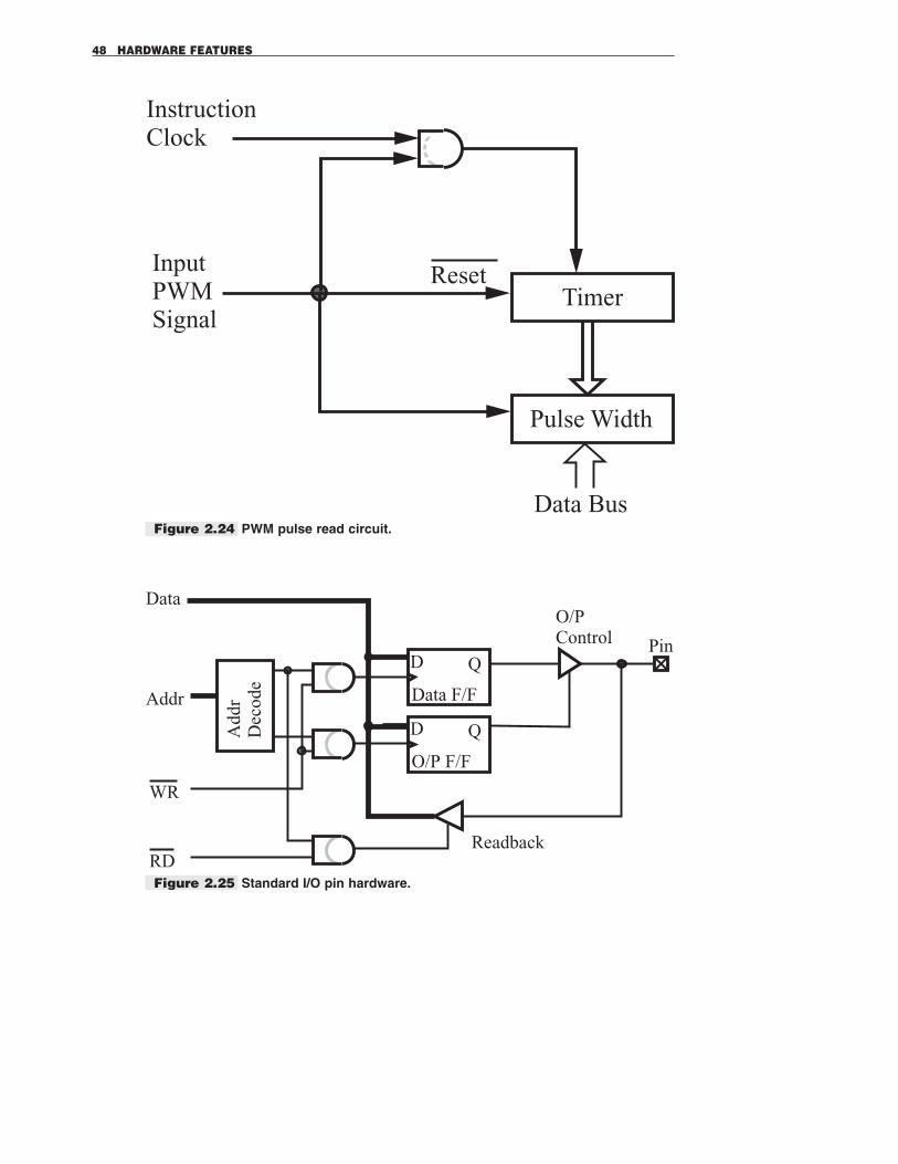
Measuring the pulse width of an input PWM waveform can be accomplished very sim-ply. (See Figure 2.24.) This circuit keeps the timer reset until the input signal goes high and
46 HARDWARE FEATURES
OverflowPrescaler Tmr1InstructionClock
Tmr2External EventSource Processor
Data Bus
Int
Figure 2.21 Microcontroller tachometer application.
Period
PulseWidth
Duty Cycle = 100% * Pulse WidthPeriod
Figure 2.22 Pulse wave modulated signal waveform.

then stops it, latches the timer value into the “pulse width” register and then resets thetimer (and disables it’s clock input) until the next pulse comes in. To make the circuit eas-ier to read and understand, I haven’t included some built-in circuit delays to make sure thatthe timer value is latched into the “duty cycle” register before the timer is reset.
Digital I/OThe basic external interface between a microcontroller and the outside world is via the dig-ital input/output (“I/O”) pins. While in many devices, these pins can be reprogrammed fordifferent set functions (such as serial and analog I/O), they are useful for providing digitalI/O. When first learning about a microcontroller, understanding how the I/O pins work(especially with different instructions) should be a very high priority.
In most devices, the pins are selectable between input and output. The typical circuitdesign for each pin is shown in Figure 2.25. The most important thing to note about thiscircuit is that reading in the bit takes the pin value, not the contents of the “data F/F”. Thismeans that if other devices connected to the pin are capable of overpowering the pins O/Pdriver, the “readback” value will be what is actually at the pin, not what is expected. Insome microcontrollers, you have the option between reading the value at the output driveror at the actual pin.
Hardware that reads the pin can cause some problems with microcontrollers that haveprocessor instructions that can read/write I/O pins in one operation. Reading in a wrongvalue will cause the data F/F to be written with an incorrect state at the end of theread/write instruction.
Another common type of common I/O pin type is the “open collector” (really “opendrain”) output. (See Figure 2.26.) In this type of pin, the pin remains at the bus state unless
DIGITAL I/O 47
INT
RO
DU
CT
ION
2
Timer
Period
Pulse Width
Reset
PWMOutput
A
B
A
B
A > B
A > BInstructionClock
Figure 2.23 PWM generator circuit.
48 HARDWARE FEATURES
Timer
Pulse Width
Reset
Instruction Clock
Input PWMSignal
Data Bus
Data F/F
QD
O/P F/F
QDAdd
rD
ecod
e
Data
Addr
WR
RDReadback
O/PControl Pin
Figure 2.24 PWM pulse read circuit.
Figure 2.25 Standard I/O pin hardware.

it is set to “output” and the bit value is “0”. When this happens, the pin is pulled to groundby the FET transistor ANDED with the output of the data F/F and O/P (output) F/F.
This type of digital I/O pin is useful for creating “dotted AND” busses which consist ofa pull up to Vcc and a number of switches or transistors able to pull the bus down. Anexample application that would use this type of bus is in a single medium bidirectional buswith multiple transmitters (each of which can put data on the bus by pulling it down).
A “typical” I/O pin can simulate the “open collector” output by remaining in input modeexcept when a “0” is to be asserted. When a “0” is to be asserted on the bus, the data F/Fwould be loaded with a “0” and then, using the O/P F/F, the pin would pull the line low.
The “O/P F/F” (or “output flip-flop) is used to control the ability of an I/O pin to drivean output value. As I have shown in the diagrams, the Data F/F and O/P F/F load clocksare individually selectable (through the use of the address bus). In some older devices, thisis not the case; often groups of 4 and 8 bits are lumped together for input/output selection.These devices may require some more planning in the circuit and software to make surethe pins work as desired.
The last aspect of I/O pins that you should be aware of is that external inputs can beused to generate interrupt requests. This typically (but not always) only happens when thepins are in input mode (this is to prevent changing the output state and causing an inter-rupt request).
Level ConversionOften when working with microcontrollers you will have to interface devices of differentlogic families together. For standard positive logic families (i.e., TTL to CMOS), this is nota problem; the devices can be connected directly. But interfacing a negative logic to a pos-itive logic family (i.e., ECL to CMOS) can cause some problems.
LEVEL CONVERSION 49
INT
RO
DU
CT
ION
2
Data F/F
QD
O/P F/F
QDAdd
rD
ecod
e
Data
Addr
WR
RDReadback
O/PControl
Pin
Figure 2.26 Open collector I/O pin hardware.

While there are usually chips available for providing this interface function (for bothinput and output), typically they only work in only one direction (which precludes bidi-rectional busses, even if the logic family allows it) and the chips can add a significant costto the application.
The most typical method of providing level conversion is to match the switching thresh-old voltage levels of the two logic families. As shown in Figure 2.27, the “ground” levelfor the COMS microcontroller has been shifted below ground (the microcontroller’s“ground” is actually the “CMOS “0”” level) so that the point where the microcontroller’sinput logic switches between a “0” and a “1” (known as the “input logic threshold” volt-age) is the same as the ECL logic. The resistor (which is between 1K and 10K) is used tolimit the current flow due to the different logic swings of the two different families.
Looking at the circuit block diagram, you’re probably thinking that the cost of shift-ing the microcontroller power supply is much greater than just a few interface chips.Actually, this isn’t a big concern because of the low power requirements of modernCMOS microcontrollers. In the example above, the ECL logic’s -5V reference can beproduced by placing a silicon diode (which has a 0.7 voltage drop across it) from themicrocontroller’s ground to the ECL’s -2-volt power supply negative output (and the -5-volt supply is referenced from “ground” of the -2-volt supply) to balance the logicthresholds. This example may seem simplistic, but it would provide the ability to con-nect a CMOS 0 to �5-volt microcontroller to ECL logic (and allow signals to be sentbidirectionally) at a very low cost.
50 HARDWARE FEATURES
ECL P/S
ECL Logic CMOS MCU
Offset P/S
MCU P/S
R
Ground
ECL "0"
ECL "1" Logic "Threshold"
CMOS "0"
CMOS "1"
Figure 2.27 ECL to CMOS logic level conversion.

Serial I/OMost intersystem (or intercomputer) communications are done serially. This means that abyte of data is sent over a single wire, one bit at a time with the timing coordinated betweenthe sender and the receiver. The obvious advantage of transmitting data serially is thatfewer connections are required.
There are a number of common serial communication protocols that are used by micro-controllers. In some devices, these protocols are built into the chip itself, to simplify theeffort required to develop software for the application.
ASYNCHRONOUS SERIAL COMMUNICATIONSThe most common form of serial communications is “asynchronous,” in which a data byte issent as a “packet” along with data start and stop information and error detection information.
The first bit sent isn’t a data bit at all, but it’s a “start bit” indicating that a data packetis being sent and is following. This is used by the receiver to synchronize the reading ofthe data which follows (least significant bit first).
A “parity bit” can optionally be sent after the data to ensure that the receiver hasreceived the correct data. There are typically two types of parity sent. “Odd parity” meansthat if the number of set (or “1”) bits and the parity bit are totaled, the sum would be anodd number (i.e., 0x055 would have a parity bit of “1” to make the total number of bitssent equal to 5, which is odd). “Even parity” is the opposite (for the example of sending0x055, the parity bit would be “0”).
In some microcontrollers, the parity has to be calculated manually and then entered intoa register. A simple algorithm for doing this is to take the byte to be transmitted and XORall the bits together, as the following 8051 code shows:
mov Count, 8 ; Do all 8 Bitsmov A, 0 ; Start Out With Nothing in “A”
P_Loop ; Come Back Here for Each Bitxrl A, Char ; XOR the LSB with LSB in “A”rrc A ; Rotate Char Over to Put the Next Bit in Positiondjnz Count, P_Loop ; Repeat 8x
The value in the least significant bit of “A” will be the “even” parity value for “Char.”That is to say, if all the bits are totaled and added to the least significant of “A,” the sumwill be even. To get “odd” parity, the least significant bit of “A” should be XORed with 1.
After the parity bit, there is a “stop bit” that is used by the receiver to store and processthe data byte just read in from the packet.
An asynchronous data packet (with 5 bits of data) looks like Figure 2.28. There are anumber of options that you should be aware of. The number of bits that are sent is appli-cation definable. In Figure 2.28, I only show 5 bits (which was the original number usedin teletypes), but as many as 8 bits can be sent in the data packet.
Along with “odd” and “even” parity, there is also “no,” “mark,” and “space” parity.“No” parity means that no parity bit is transmitted with the data in the packet. “Mark” or“space” parity means that a “1” or “0,” respectively, is always sent after the data in thepacket. This type of parity is very rarely used, and when it is used, the reason for its use isto allow the receiver time to process the data before the next data byte comes along.
SERIAL I/O 51
INT
RO
DU
CT
ION
2

The number of stop bits is also an option, for the same reasons as mark and space par-ity. A second stop bit can be inserted in the data packet to give the receiver more time toprocess the received byte before preparing to receive the next one.
In virtually all modern asynchronous communications, the data format is “8-N-1,”which means 8 data bits, no parity, and one stop bit as the packet format. The parity andadditional end interval are generally not required for serial communications.
The most popular type of asynchronous serial communication is known as “RS-232,”which is now an EIA standard. This is a very old standard used to connect different comput-ers. I discuss interfacing to RS-232 in the “Common Microcontroller Interfaces” chapter.
The asynchronous receiver hardware waits for the “start bit.” When the input line goes low(indicating a start bit), the input line is polled one-half bit later (which is timed by an over-speed clock). If the line is still low (if it’s not, then the receiver assumes that the low was a“glitch” and data bits won’t be received), then the receiver waits one bit period and reads inthe data. (See Figure 2.29.) This method is used for both hardware and software asynchronousdata receiving (in software receivers, a timed loop is used for the half bit and full bit delays).
Another common method of serially transmitting data asynchronously is to use the“manchester” encoding format. In this type of data transfer, each bit is synchronized to apulse and the type of bit is dependent on the length of time until the next pulse. (Figure2.30.) In this type of data transmission, the data size is known so the “stop pulse” is rec-ognized and the space afterward is not treated as incoming data.
Manchester encoding is unique in that the “start bit” of a packet is quantitatively dif-ferent from a “1” or a “0.” This allows a receiver to determine whether or not the data pack-et being received is actually at the start of the packet or somewhere in the middle (andshould be ignored until a start bit is encountered).
Manchester encoding is well suited for situations where data can be easily interrupted.Because of this, it is the primary method of data transmission for infrared control (such asused in your TV’s remote control).
Synchronous Serial CommunicationsFor synchronous data communications in a microcontroller, a clock signal is sent along withserial data. (Figure 2.31.) This clock signal is used by the receiver to strobe in the data.
52 HARDWARE FEATURES
StartBit
Data Bits
ParityBit
StopBit
Bit 0 Bit 1 Bit 0 Bit 3 Bit 4
Figure 2.28 Asynchronous serial data stream.

SYNCHRONOUS SERIAL COMMUNICATIONS 53
INT
RO
DU
CT
ION
2
StartBit
BitReading
Overspeed Clock
Figure 2.29 Reading an asynchronous serial data stream.
StartBit
Data Bits
StopPulse
"0""1"
Figure 2.30 Manchester encoded serial data.
Clock
DataFigure 2.31 Synchronous data waveform.

A typical circuit, using discrete devices, is shown in Figure 2.32. This circuit convertsserial data into eight digital outputs, which all are available at the same time (when the“O/P latch” is strobed). For most applications, the second ‘374 providing the parallel datais not required. This serial-to-parallel conversion can also be accomplished using serial-to-parallel chips, but I prefer using 8-bit registers because they are generally easier to findthan other TTL parts.
There are two very common synchronous data protocols: Microwire and SPI. Thesemethods of interfacing are used in a number of chips (such as the serial EEPROMs usedin the BASIC Stamps). While the Microwire and SPI standards are quite similar, there area number of differences that should be noted.
I consider these protocols to be methods of transferring synchronous serial data ratherthan microcontroller network protocols because each device is individually addressed(even though the clock/data lines can be common between multiple devices). If the chipselect for the device is not asserted, the device ignores the clock and data lines. With theseprotocols, only a single “master” can be on the bus. (Figure 2.33.)
If a synchronous serial port is built into the microcontroller, the transmit circuitry mightlook like Figure 2.34. This circuit will shift out 8 bits of data. For protocols like microwirewhere a “start bit” is initially sent, the “start bit” is sent using direct reads and writes to theI/O pins. To receive data, a similar circuit would be used, but data would be shifted into theshift register and then read by the microcontroller.
MICROWIREThe Microwire protocol is capable of transferring data at up to one megabit per second.Sixteen bits are transferred at a time.
54 HARDWARE FEATURES
Mic
roco
ntro
ller
Data
Clock
O/PLatch
74LS374 74LS374
OE
1D
1Q
2Q
2D
3D
3Q
4D
8Q
OE
1D
2D
3D
8D
1Q
2Q
3Q
8Q
Figure 2.32 Synchronous serial-to-parallel output circuit.

SYNCHRONOUS SERIAL COMMUNICATIONS 55
INT
RO
DU
CT
ION
2
Mic
roco
ntro
ller
Data Out
Clock
Data In
SynchDevice#2Din
Dout
CSDev #2
Dev #1
SynchDevice#1Din
Dout
CS
Figure 2.33 Synchronous serial device bus.
Figure 2.34 Synchronous output circuit.
TimerPWMOutput
1-8Cntr
Shift Register
Start DataSentSignal
MCUDataBus
Clk
DO

To read 16 bits of data, the waveform would look like Figure 2.35. After selecting a chipand sending a start bit, the clock strobes out an 8-bit command byte (labelled “OP1,”“OP2,” “A5” to “A0” in Figure 2.35), followed by (optionally) a 16-bit address word trans-mitted and then another 16-bit word either written or read by the microcontroller.
With a one megabit per second maximum speed, the clock is both high and low for 500nsecs. Transmitted bits should be sent 100 nsecs before the rising edge of the clock. Whenreading a bit, it should be checked 100 nsecs before the falling edge of the clock. While thesetimings will work for most devices, you should make sure you understand the requirementsof the device being interfaced to.
SPIThe SPI protocol is similar to Microwire, but with a few differences.
1. SPI is capable of up to 3 megabits per second data transfer rate.2. The SPI data “word” size is 8 bits.3. SPI has a “hold” which allows the transmitter to suspend data transfer.4. Data in SPI can be transfered as multiple bytes known as “blocks” or “pages.”
Like Microwire, SPI first sends a byte instruction to the receiving device. After the byteis sent, a 16-bit address is optionally sent, followed by 8 bits of I/O. As noted above, SPIdoes allow for multiple byte transfers. (Figure 2.36.)
The SPI clock is symmetrical (an equal low and high time). Output data should be avail-able at least 30 nsecs before the clock line goes high and read 30 nsecs before the fallingedge of the clock.
When wiring up a Microwire or SPI device, the one trick that you can do to simplifythe microcontroller connection is to combine the “DI” and “DO” lines into one pin.(Figure 2.37.)
56 HARDWARE FEATURES
CS
Clock
DI
DO
SB
OP
1
OP
2
A5
A4
A0
D15
Figure 2.35 Microwire data read.

SYNCHRONOUS SERIAL COMMUNICATIONS 57
INT
RO
DU
CT
ION
2
CS
Clock
DI
DO
D7Instruction
I7 I6 I5 I4 I3 I0
Figure 2.36 SPI data write.
Mic
roco
ntro
ller
Data
ClockSynchDevice
DinDout
CSDev Sel
1K-10K
Figure 2.37 Combining D0 and DI from a synchronous serial device.

In this method of connecting the two devices, when the data pin on the microcontrollerhas completed sending the serial data, the output driver can be turned off and the micro-controller can read the data coming from the device. The current-limiting resistor betweenthe “data” pin and “DI”/“DO” limits any current flows when both the microcontroller anddevice are driving the line.
Network CommunicationsWhen I discuss networking with regards to microcontrollers, I’m generally talking aboutbusses used to connect additional hardware devices to the microcontrollers and allowingcommunications between microcontrollers. (This is opposed to “local area networks”(“LANs”), like “Ethernet” that you were probably thinking about when you saw the word“networks.”)
There are a variety of standards (which can be broadened to include Microwire and SPIdiscussed in the previous subsection), which leads to some confusion over what is andwhat isn’t a network. I personally define a microcontroller network as a single communi-cations medium (i.e., wire) and multiple devices connected to this medium which can ini-tiate message transfers and respond to messages directed towards them.
In these types of networks, a “master” is an intelligent device which can initiate datatransfers. Devices which respond to requests (and can’t initiate them) are known as“slaves.” Microcontroller networks can have multiple masters, which means the networkprotocol requires an arbitration scheme which allows multiple masters to transmit withoutruining each other’s messages.
Typically, microcontroller networks transmit very little data, so the bandwidth required isquite modest when compared to something like an ethernet-connected PC that has an ownerwho is a Web surfer. It’s not unusual to have a microcontroller network that is transferringbytes per second (compared to a PC network that may transfer megabytes per second).
I will introduce you to two of the most popular microcontroller networks, and whilewhat I have written is quite complete, it’s not sufficient to use as a reference for develop-ing network applications. If you are planning on using these network protocols, you willhave to get more information, in the form of device datasheets or standards specifications.What I have done is given you enough information to understand the basics of the proto-cols and evaluate them for an application, to decide which is the most appropriate.
I2CThe most popular form of a microcontroller network is “I2C,” which stands for “inter-intercomputer communicaitons.” This standard was originally developed by Philips inthe late 1970s as a method to provide an interface between microprocessors and periph-eral devices without wiring full address, data, and control busses between devices. I2C also allows sharing of network resources between processors (which is known as“multimastering”).
The I2C bus consists of two lines: a clock line (“SCL”) which is used to strobe data(from the “SDA” line) from or to the master that currently has control over the bus. Boththese bus lines are pulled up (to allow multiple devices to drive them).
58 HARDWARE FEATURES

A I2C controlled stereo system might be wired as shown in Figure 2.38. The two buslines are used to indicate that a data transmisstion is about to begin as well as pass the dataon the bus.
To begin a data transfer, a “start condition” is put on the bus. Normally, (when the busis in the “idle state,” both the clock and data lines are not being driven (and are pulledhigh). To initiate a data transfer, the master requesting the bus pulls down the SDA bus linefollowed by the SCL bus line. During data transmission, this is an invalid condition(because the data line is changing while the clock line is active/high).
To end data transmission, the reverse is executed: the clock line is allowed to go high,which is followed by the data line. (Figure 2.39.)
NETWORK COMMUNICATIONS 59
INT
RO
DU
CT
ION
2MainProcessor
I/R Remote
TapeDeck
CDPlayer
Amplifier Tuner
Vcc
SCL(Clock)SDA(Data)
1K - 10KPull Ups
Figure 2.38 Example I2C network wiring.
SCL
SDA
LineIdle
StartCond'n
BitXtmit
StopCond'n
LineIdle
Figure 2.39 I2C signals and waveforms.

Data is transmitted in a synchronous fashion, with the most significant bit sent first andafter 8 bits are sent, the master allows the data line to float (it doesn’t drive it low) whilestrobing the clock to allow the receiving device to pull the data line low as an acknowl-edgment that the data was received. After the acknowledge bit, both the clock and datalines are pulled low in preparation for the next byte to be transmitted, or a stop/start con-dition is put on the bus. (Figure 2.40.)
Sometimes the acknowledge bit will be allowed to float high, even though the datatransfer has completed successfully. This is done to indicate that the data transfer has com-pleted and the receiver (which is usually a “slave device” or a “master” which is unable toinitate data transfer) can prepare for the next data request.
There are two maximum speeds for I2C (because the clock is produced by a master,there really is no minimum speed); “standard mode” runs at up to 100 kbps and “fastmode” can transfer data at up to 400 kbps. (Figure 2.41.)
A command is sent from the master to the receiver in the format shown in Figure 2.42.The “receiver address” is 7 bits long and is the bus address of the receiver. There is a loosestandard, which is the most significant four bits are used to identify the type of device,while the next three bits are used to specify one of eight devices of this type (or furtherspecify the device type).
As I said above, this is a “loose standard.” Some devices require certain patterns for thesecond three bits, while others (such as some large serial EEPROMS) use these bits tospecify an address inside the device. There is also a 10-bit address standard in which thefirst 4 bits are all set, the next bit is reset, the last 2 bits are the most significant of theaddress, and the final 8 bits are sent in a following byte. All this means is that it is veryimportant to map out the devices to be put on the bus and all their addresses.
The following first four bit patterns generally follow the following convention for dif-ferent devices:
0000 - Reserved address0010 - Voice synthesizer0011 - PCM audio interface0100 - Audible tone generation
60 HARDWARE FEATURES
SCL
SDA
Bit 7 Bit 6 Bit 5 Bit 4 Bit 3 Bit 2 Bit 1 Bit 0 AckBit
Transmitter ReceiverFigure 2.40 I2C data byte transmission.

0111 - LCD/LED displays1000 - Video interface1001 - A/D and D/A interfaces1010 - Serial memory1100 - RF tuning/control1101 - Clock/calendar1111 - Reserved/10-bit address
NETWORK COMMUNICATIONS 61
INT
RO
DU
CT
ION
2SCL
SDA
StartCond'n
BitXtmit
StopCond'n
LineIdle
Std.Fast
4.00.6
4.71.3
4.00.6
4.00.6
4.71.4
All Times are Minimum ValuesAll Times in uSecondsFigure 2.41 I2C signal timing.
Start Condition
ReceiverAddress R
/W
Ack
StopCondtion
Ack
AdditionalData/StartCommands
DataTX/RX
Figure 2.42 I2C data transmission.
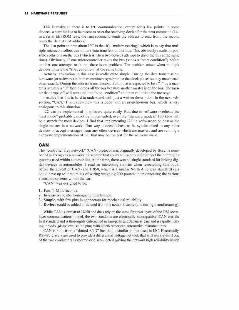
This is really all there is to I2C communication, except for a few points. In somedevices, a start bit has to be resent to reset the receiving device for the next command (i.e.,in a serial EEPROM read, the first command sends the address to read from, the secondreads the data at that address).
The last point to note about I2C is that it’s “multimastering,” which is to say that mul-tiple microcontrollers can initiate data transfers on the bus. This obviously results in pos-sible collisions on the bus (which is when two devices attempt to drive the bus at the sametime). Obviously, if one microcontroller takes the bus (sends a “start condition”) beforeanother one attempts to do so, there is no problem. The problem arises when multipledevices initiate the “start condition” at the same time.
Actually, arbitration in this case is really quite simple. During the data transmission,hardware (or software) in both transmitters synchronize the clock pulses so they match eachother exactly. During the address transmission, if a bit that is expected to be a “1” by a mas-ter is actually a “0,” then it drops off the bus because another master is on the bus. The mas-ter that drops off will wait until the “stop condition” and then re-initiate the message.
I realize that this is hard to understand with just a written description. In the next sub-section, “CAN,” I will show how this is done with an asynchronous bus, which is veryanalogous to this situation.
I2C can be implemented in software quite easily. But, due to software overhead, the“fast mode” probably cannot be implemented; even the “standard mode’s” 100 kbps willbe a stretch for most devices. I find that implementing I2C in software to be best as thesingle master in a network. That way it doesn’t have to be synchronized to any otherdevices or accept messages from any other devices which are masters and are running ahardware implementation of I2C that may be too fast for the software slave.
CANThe “controller area network” (CAN) protocol was originally developed by Bosch a num-ber of years ago as a networking scheme that could be used to interconnect the computingsystems used within automobiles. At the time, there was no single standard for linking dig-ital devices in automobiles. I read an interesting statistic when researching this book;before the advent of CAN (and J1850, which is a similar North American standard) carscould have up to three miles of wiring weighing 200 pounds interconnecting the variouselectronic systems within the car.
“CAN” was designed to be:
1. Fast (1 Mbit/second).2. Insensitive to electromagnetic interference.3. Simple, with few pins in connectors for mechanical reliability.4. Devices could be added or deleted from the network easily (and during manufacturing).
While CAN is similar to J1850 and does rely on the same first two layers of the OSI seven-layer communications model, the two standards are electrically incompatible. CAN was thefirst standard and is thoroughly entrenched in European and Japanese cars and is rapidly mak-ing inroads (please excuse the pun) with North American automotive manufacturers.
CAN is built from a “dotted AND” bus that is similar to that used in I2C. Electrically,RS-485 drivers are used to provide a differential voltage network that will work even if oneof the two conductors is shorted or disconnected (giving the network high reliability inside
62 HARDWARE FEATURES
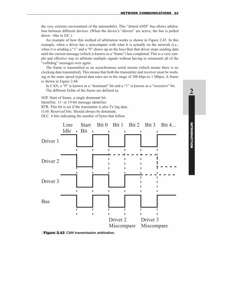
the very extreme environment of the automobile). This “dotted AND” bus allows arbitra-tion between different devices. (When the device’s “drivers” are active, the bus is pulleddown—like in I2C.)
An example of how this method of arbitration works is shown in Figure 2.43. In thisexample, when a driver has a miscompare with what it is actually on the network (i.e.,when it is sending a “1” and a “0” shows up on the bus) then that driver stops sending datauntil the current message (which is known as a “frame”) has completed. This is a very sim-ple and effective way to arbitrate multiple signals without having to retransmit all of the“colliding” messages over again.
The frame is transmitted as an asynchronous serial stream (which means there is noclocking data transmitted). This means that both the transmitter and receiver must be work-ing at the same speed (typical data rates are in the range of 200 kbps to 1 Mbps). A frameis shown in Figure 2.44:
In CAN, a “0” is known as a “dominant” bit and a “1” is known as a “recessive” bit.The different fields of the frame are defined as:
SOF. Start of frame, a single dominant bit.Identifier. 11- or 19-bit message identifier.RTR. This bit is set if the transmitter is also Tx’ing data.r1/r0. Reserved bits. Should always be dominant.DLC. 4 bits indicating the number of bytes that follow.
NETWORK COMMUNICATIONS 63
INT
RO
DU
CT
ION
2
Driver 1
Driver 2
Driver 3
Bus
StartBit
LineIdle
Bit 0 Bit 1 Bit 2 Bit 3 Bit 4...
Driver 2Miscompare
Driver 3Miscompare
Figure 2.43 CAN transmission arbitration.

Data. 0 to 8 bytes of data, sent MSB first.CRC. 15 bits of CRC data followed by a recessive bit.Ack. 2-bit field, dominant/recessive bits.EOF. End of frame, at least 7 recessive bits/.
The last important note about CAN is that devices are not given specific names oraddresses. Instead, the message is identified (using the 11- or 19-bit message identifier).This method of addressing can provide you with very flexible messaging (which is whatCAN is all about).
The CAN “frame” is very complex, as is the checking that has to be done, both forreceiving a message and transmitting a message. While it can be done using a microcon-troller and programming the functions in software, I would recommend only implement-ing CAN using hardware interfaces. There are several microcontroller vendors which pro-vide CAN interfaces as part of the devices, and there are quite a few different “standard”chips (the Intel 82527 is a very popular device) available which will carry out CAN inter-face functions for you effectively and cheaply.
Analog I/OThe world outside the microcontroller is not all black and white (or ones and zeros); it isreally varying shades of grey (or values between zero and one). Often a microcontrollerwill have to interface with analog signals (between Vcc and ground), both receiving them(and interpreting the value) as well as outputting them. In many models of the differentmicrocontroller families there are analog-to-digital convertors (“ADCs”) and digital-to-analog convertors (“DACs”). In this subsection, I will introduce you to analog voltage I/O,not analog data communication, which is discussed in the “Timer” section of this chapter(which describes sending and receiving PWM data).
There are three types of analog voltage input for microcontrollers. The first is a physi-cal positional control sensor in which the microcontroller determines the position of apotentiometer. Next, an analog voltage comparator can be used to determine whether ornot an input voltage is greater than or less than a reference voltage. The last type of ADCused in microcontrollers is known as an “integrating ADC,” which can determine a volt-age level independently. Each of these different types of ADCs are best suited for differentapplications.
64 HARDWARE FEATURES
Identifier DLC Data (0 - 8 Bytes) CRCLineIdle
SOFRTR
r1/r0
Ack
EOFFigure 2.44 CAN 11-bit identifier frame.
The first type of ADC isn’t really an ADC at all, but a method of reading a poten-tiometer’s current resistance using digital I/O pins. To read the resistance, a simple RC net-work is attached to a microcontroller I/O pin. (Figure 2.45.)
The potentiometer resistance is read by measuring how long the voltage of the currentflowing from the charged capacitor through the potentiometer is above the digital thresh-old level. The higher the resistance, the longer the input is read as a “1.” (Figure 2.46.)
To measure the discharge cycle, the I/O pin is enabled as an output and set to a “1.” Thecap is allowed to charge to Vcc (through “Rsub,” which limits current to prevent short cir-cuit currents when the cap is initially charged). Once the cap is fully charged, the pin out-put driver is disabled and the cap is allowed to discharge through the potentiometer. Themeasurement ends when the voltage goes below “Vthreshold.” Typically, a timer is used totime how long the voltage is above threshold.
If you were to look at this operation on an oscilloscope, you would see the waveformshown in Figure 2.46. To determine the values for R & C (Rsub is usually in the range of100 to 200 Ohms), you can use the approximation:
t � 2.2 � R � C
Where “t” is the time for the time required to discharge the capacitor.When I say that this will give you the “approximate” time, I mean to say that it will real-
ly only get you in the ballpark. This is generally not a precision circuit because of the tol-erances of the resistor and capacitor and the nonlinear behaviour of the CMOS input bit.You can get more exact values by specifying a precision capacitor (which is often hard tofind and expensive), but for the circuit, the application shouldn’t really require it.
ANALOG I/O 65
INT
RO
DU
CT
ION
2
Microcontroller
C
PotRsub
Vcc
Figure 2.45 Using digital I/O pins to read a potentiometer.

Now you’re probably asking yourself, if this is a very imprecise method of reading apotentiometer, where and why is it used? It’s used in circuits that simply provide a relativevalue for the potentiometer’s position. For example, the IBM PC uses this type of circuitto read the current joystick postion. This imprecision is often reflected in the games wherethe user is asked to move the joystick to extremes to “train” the program in how the capac-itor and joystick resistors interact.
Typically, I use a 0.1-uF tantalum cap and a 10K potentiometer for this circuit. Thisgives me an approximate maximum time delay of 22 msecs, which is long enough fora microcontroller to accurately read the time delay and is fast enough that the userwon’t be aware that the resistance measurement is taking place. I use a 0.1 tantalum capbecause I use them for decoupling Vcc and ground in devices, and I always have abunch of them around. The problem with using tantalum caps is that they can often beout by as much as 100% from their rated value. This means that I usually have themicrocontroller “calibrate” the extreme values of the potentiometer before the applica-tion is usable.
The next type of ADC commonly available in microcontrollers is the analog voltagecomparator. A comparator is a simple circuit which compares two voltages and returns a“1” when the input signal voltage is greater than the reference voltage (“Vref ”). (Figure2.47.) This circuit is best used for applications like thermostats, where something happensat specific input voltage points.
Often, in microcontrollers that use comparators for ADCs, the reference voltage(“Vref ”) is generated internally using a resistor ladder and an analog multiplexer to selectthe desired voltage to output. (Figure 2.48.)
This circuit can actually give some modicum of voltage specification. A simple algo-rithm could be used to run through each of the different voltages until the comparator out-put changes. The point of change is the actual input voltage. The reason why I say thisgives a “modicum” of voltage determination is because typically the Vref circuit has a fair-ly wide range between each voltage step (this is also known as a large “granularity”). If the
66 HARDWARE FEATURES
V
t
ChargeCap
DischargeCap toVthreshold
Vthreshold
Figure 2.46 Electrical waveform for reading a potentiometer.
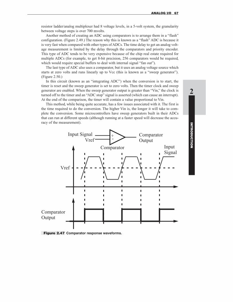
resistor ladder/analog multiplexer had 8 voltage levels, in a 5-volt system, the granularitybetween voltage steps is over 700 mvolts.
Another method of creating an ADC using comparators is to arrange them in a “flash”configuration. (Figure 2.49.) The reason why this is known as a “flash” ADC is because itis very fast when compared with other types of ADCs. The time delay to get an analog volt-age measurement is limited by the delay through the comparators and priority encoder.This type of ADC tends to be very expensive because of the chip real estate required formultiple ADCs (for example, to get 8-bit precision, 256 comparators would be required,which would require special buffers to deal with internal signal “fan out”).
The last type of ADC also uses a comparator, but it uses an analog voltage source whichstarts at zero volts and runs linearly up to Vcc (this is known as a “sweep generator”).(Figure 2.50.)
In this circuit (known as an “integrating ADC”) when the conversion is to start, thetimer is reset and the sweep generator is set to zero volts. Then the timer clock and sweepgenerator are enabled. When the sweep generator output is greater than “Vin,” the clock isturned off to the timer and an “ADC stop” signal is asserted (which can cause an interrupt).At the end of the comparison, the timer will contain a value proportional to Vin.
This method, while being quite accurate, has a few issues associated with it. The first isthe time required to do the conversion. The higher Vin is, the longer it will take to com-plete the conversion. Some microcontrollers have sweep generators built in their ADCsthat can run at different speeds (although running at a faster speed will decrease the accu-racy of the measurement).
ANALOG I/O 67
INT
RO
DU
CT
ION
2
InputSignal
Vref
ComparatorOutput
+-
ComparatorOutput
Comparator
VrefInput Signal
Figure 2.47 Comparator response waveforms.
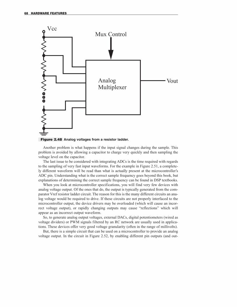
Another problem is what happens if the input signal changes during the sample. Thisproblem is avoided by allowing a capacitor to charge very quickly and then sampling thevoltage level on the capacitor.
The last issue to be considered with integrating ADCs is the time required with regardsto the sampling of very fast input waveforms. For the example in Figure 2.51, a complete-ly different waveform will be read than what is actually present at the microcontroller’sADC pin. Understanding what is the correct sample frequency goes beyond this book, butexplanations of determining the correct sample frequency can be found in DSP textbooks.
When you look at microcontroller specifications, you will find very few devices withanalog voltage output. Of the ones that do, the output is typically generated from the com-parator Vref resistor ladder circuit. The reason for this is the many different circuits an ana-log voltage would be required to drive. If these circuits are not properly interfaced to themicrocontroller output, the device drivers may be overloaded (which will cause an incor-rect voltage output), or rapidly changing outputs may cause “reflections” which willappear as an incorrect output waveform.
So, to generate analog output voltages, external DACs, digital potentiometers (wired asvoltage dividers) or PWM signals filtered by an RC network are usually used in applica-tions. These devices offer very good voltage granularity (often in the range of millivolts).
But, there is a simple circuit that can be used on a microcontroller to provide an analogvoltage output. In the circuit in Figure 2.52, by enabling different pin outputs (and out-
68 HARDWARE FEATURES
AnalogMultiplexer
Vcc
Vout
Mux Control
Figure 2.48 Analog voltages from a resistor ladder.
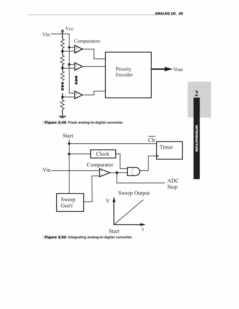
ANALOG I/O 69
INT
RO
DU
CT
ION
2
PriorityEncoder
Vcc
Vout
VinComparators+-
+-
+-
Figure 2.49 Flash analog-to-digital converter.
Vin
ADCStop
Start
ClockTimer
SweepGen'r
V
tStart
Sweep Output
Clr
Comparator+-
Figure 2.50 Integrating analog-to-digital converter.
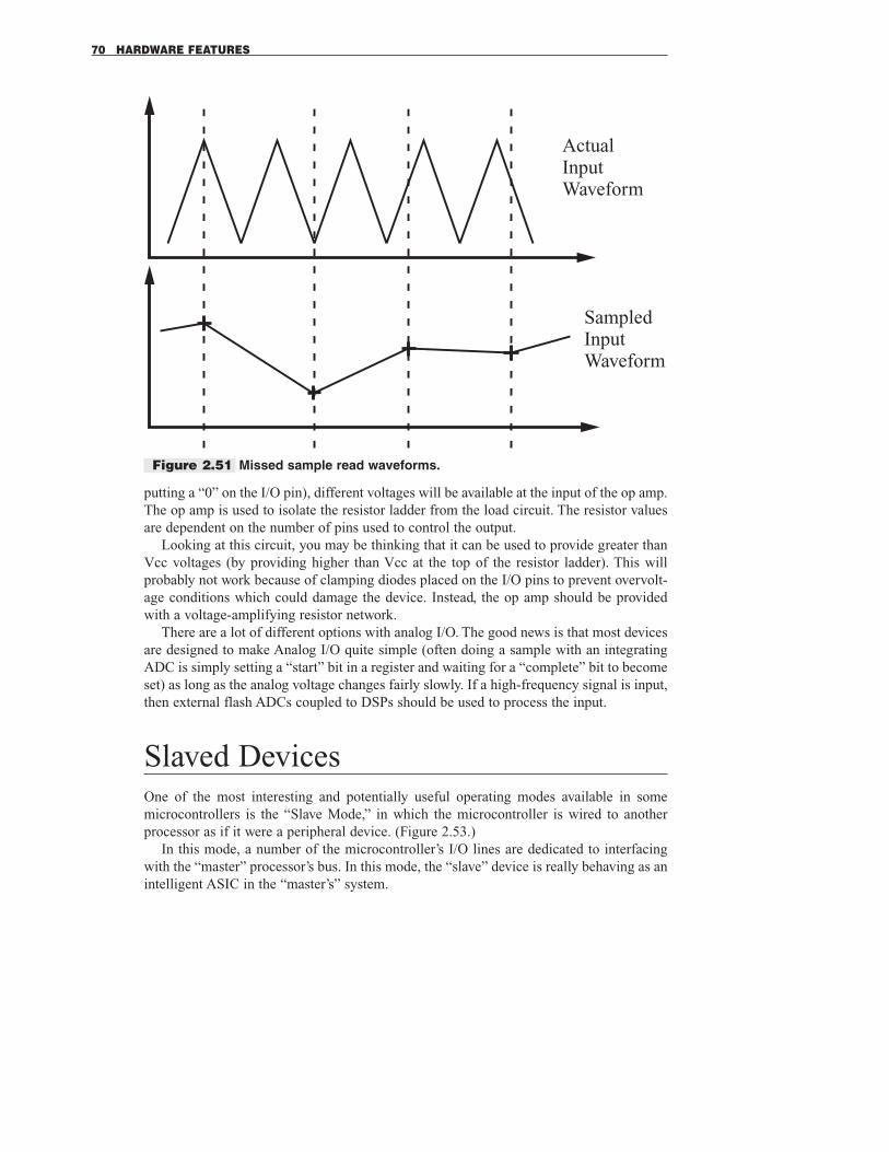
putting a “0” on the I/O pin), different voltages will be available at the input of the op amp.The op amp is used to isolate the resistor ladder from the load circuit. The resistor valuesare dependent on the number of pins used to control the output.
Looking at this circuit, you may be thinking that it can be used to provide greater thanVcc voltages (by providing higher than Vcc at the top of the resistor ladder). This willprobably not work because of clamping diodes placed on the I/O pins to prevent overvolt-age conditions which could damage the device. Instead, the op amp should be providedwith a voltage-amplifying resistor network.
There are a lot of different options with analog I/O. The good news is that most devicesare designed to make Analog I/O quite simple (often doing a sample with an integratingADC is simply setting a “start” bit in a register and waiting for a “complete” bit to becomeset) as long as the analog voltage changes fairly slowly. If a high-frequency signal is input,then external flash ADCs coupled to DSPs should be used to process the input.
Slaved DevicesOne of the most interesting and potentially useful operating modes available in somemicrocontrollers is the “Slave Mode,” in which the microcontroller is wired to anotherprocessor as if it were a peripheral device. (Figure 2.53.)
In this mode, a number of the microcontroller’s I/O lines are dedicated to interfacingwith the “master” processor’s bus. In this mode, the “slave” device is really behaving as anintelligent ASIC in the “master’s” system.
70 HARDWARE FEATURES
ActualInputWaveform
SampledInputWaveform
Figure 2.51 Missed sample read waveforms.

The first application where I saw this mode used was in the IBM PC/AT. An Intel 8042is used as the keyboard interface (along with some other features) to allow the centralprocessor to simply read and write data, rather than having to interface directly with theserial keyboard (and having to execute the keyboard serial protocol).
Not shown in Figure 2.53, the microcontroller can interrupt the “master” by using one ofits I/O pins to drive one of the master’s interrupt request lines. I should point out that somedevices can work in a “microprocessor” mode where the microcontroller is driving the buses.
SLAVED DEVICES 71
INT
RO
DU
CT
ION
2Microcontroller
Vcc
AnalogO/O
OP Amp
+-
Figure 2.52 Analog voltage output circuit.
"Master"Processor
AddrDecode
"Slave"Microcontroller
CS
RDWR
D7:0
RDWR
D7:0
Addr
Figure 2.53 Microcontroller slaved to master.

Device ProgrammingOften you will use E(E)PROM-based microcontrollers for developing your applications aswell as shipping in your product. Elsewhere in the book, I have discussed the advantagesof this type of device over ROM-based programming. The disadvantage of this type ofmicrocontroller is that you have to program it.
This is usually done by loading a holding register with the value you want to programinto a location, then triggering a circuit for burning the contents of the holding location ata specific address, waiting some period of time for the programming to complete, and thenverifying what you have written. Programming a full device can take anywhere from a fewseconds to a few minutes, depending on the size of the device and the algorithms used forprogramming.
Often the programming equipment is very expensive (especially for the hobbyist/smallbusiness) and can be controller (i.e., PC or workstation) specific. But there are cases wherethe programming equipment is quite reasonable and simple. For example, when I discussthe PIC and AVR, I know you’ll be amazed at how simple a device can be used to programsome versions of them. There are also devices where no programming equipment isrequired (such as the Basic STAMP) or has built-in hardware and software which elimi-nates the need for external hardware other than supplying power to the device to be pro-grammed (the 68HC05).
A very important aspect of the programming of a device is whether or not it can be“in system” programmed (“ISP”). If a microcontroller is said to be ISP capable, itmeans that a blank device can be soldered into a circuit and then have it programmedwithout affecting any of the other devices in the circuit. This can be an important con-sideration when choosing a device; implementing an ISP device in a circuit can elimi-nate the requirement to buy a unique programmer, allow software updates without hav-ing to pull stock, and allow the manufacturer to carry stock that is not unique to a spe-cific product.
CONTROL STORE SECURITYFor many applications it may be desirable to protect the code burned into the microcontroller.To help aid in this, most devices provide some method of preventing the program being readfrom the device. Often this is done by setting a configuration bit during programming.
This bit is usually designed to be only cleared after the information in the rest of thechip is cleared (i.e., by ultraviolet light in the case of an EPROM-based part).
The built-in code protection will not prevent a really determined effort to read the codecontained within it. This can be done in many chip failure analysis labs (and in a surpris-ingly short time). To try and make this operation less effective, some companies scramblethe instructions loaded into the control store and then provide hardware on the chip forconverting the scrambled data back into instructions for the processor.
I’m not trying to scare you or tell you not to use the control store protect bit, but rathercaution you to the pitfalls of setting the bit as well as warning you that it is probably notthe ultimate protection of the code in the device (which is where a significant amount ofdevelopment effort has gone for the application/product).
72 HARDWARE FEATURES

Debug InterfacesMost of the devices presented here have in circuit emulators (“ICEs”) available for appli-cation debug. These devices physically replace the microcontroller in the circuit and pro-vide an interface into the operation of the device, both from a hardware and a softwarepoint of view. Often, ICE developers will provide an integrated interface between the soft-ware development system (editor and compiler) and the emulator, allowing real-timedebug of the software and application without time-consuming erasure and reprogram-ming, or setting up of serial I/O (or even LEDs) to determine the operation of the micro-controller. The only issue with these devices is the cost, which can be in the thousands ofdollars.
Some microcontrollers do provide serial interfaces as part of hardware that is specificto debugging an application. These interfaces allow uploading and downloading of pro-grams, data, and register contents as well as provide an execution interface to allow theuser to start or stop the microcontroller remotely (and then download the variables/RAMcontent to see how the program executed). When coupled with a comprehensivecontrol/interface program, this type of interface can replace an ICE for program develop-ment or manufacturing debug (and at a considerable cost savings over the ICE). Often, thistype of interface is only available in high-pin-count and high-function microcontrollers,but it is available in some of the lower cost/function devices.
The last type of debugging interface is actually using specialized software to control theexecution of the application software. A “monitor program” is actually a very simple exe-cution control program that will allow you to start, stop, and modify (“patch”) the appli-cation code, read and modify variable and register contents, and single-step or stop onbreakpoint the application. In very small devices, this is probably not an option, but asdevices are available with more memory, this is becoming more possible, and there aresome devices which have monitor programs built in.
DEBUG INTERFACES 73
INT
RO
DU
CT
ION
2
