international journal of scientific & engineering … · advances in adc and dac technologies...
TRANSCRIPT

International Journal of Scientific & Engineering Research, Volume 4, Issue 8, August 2013 ISSN 2229-5518
IJSER © 2013
http://www.ijser.org
Timing Controller using FPGA MicroBlaze for a Digital Radar Receiver
Ragimol, Shajahan M
Abstract— With the popular hardware description languages in place, there is a wide range of options that enables Field Programmable Gate Array
(FPGA) designers to design optimized hardware implementation adding to the flexibility that language-based design provides the designers. Designers
get to implement flexible Intellectual Property (IP) core which is widely used for custom applications. Configurable soft processor cores that can be syn-
thesized onto their FPGA products thus enhancing configurability and programmability are being manufactured by different vendors to suit the needs of
front end users. The FPGA embedded processors use general-purpose FPGA logic to construct internal memory, processor buses, internal and external
peripherals. This paper focuses on the design of a timing control and signal generation controller on Xilinx MicroBlaze for a digital radar receiver. Micro-
Blaze enhances critical timing algorithms important for radar communications with adequate advantages such as customization, flexibility, hardware
acceleration, obsolescence mitigation and programmability with scalability. The processor environment in the FPGA fabric is utilized for providing cus-
tomization of the timing unit for signal transmission. With the selection of an appropriate FPGA family, optimized hardware with high DMIPS benchmarks
can be availed.
Index Terms— digital radar communications, FPGA, Microblaze, soft core processors, radar receiver, timing control and signal generation,
Xilinx platform studio (XPS).
—————————— ——————————
1 INTRODUCTION
ITH the progressive increase in the use of FPGAs for prototyping the embedded systems on a chip, the use of IPs is being used enhance the features of designs. To
attach an IP with one of the buses in the design, the designer has to create an interface for it, for which so as to ease this task, FPGA vendors provide the facility for automatic genera-tion of interfaces for custom IPs. Soft core processor Micro-Blaze, provided by Xilinx, is one such provision. As FPGA devices progresses both in terms of resources and perfor-mance, the latest FPGAs provides solutions that are easily cus-tomizable for system connectivity, DSP, and data processing applications. This helps leading FPGA vendors to come up with easy to use design development tools. There is an accel-erated time-to-market delivery by automating the system def-inition and integration phases of system on programmable chip development [1]. Designers are provided the facility to quickly create hardware circuits, with increases in FPGA con-figurable logic capacity. FPGAs with soft processor cores pro-vide designers with increased flexibility and scalability thus expanding the usefulness of soft processor cores on FPGAs to a broader range of applications.
Today FPGAs are used to quickly create efficient hardware designs, for which systems require a combination of both software and hardware. In earlier years, single-chip micropro-cessor/FPGA devices had been introduced [1]. These devices
include one or more hard-core microprocessors, implemented using transistors and an FPGA fabric on a single IC. Single-chip hard-core microprocessor/FPGA platforms offer excel-lent packaging and communication advantages, but a soft core approach offers the advantage of flexibility and lower part costs. FPGA vendors are now offering such soft processor cores that designers can implement using a standard FPGA. Altera offers both the NIOS and NIOS II soft processor cores [2]. The NIOS II processor is a 32-bit configurable processor supporting clock frequency as high as 135MHz. Xilinx offers the PicoBlaze and MicroBlaze soft processor cores. The Micro-Blaze processor is a 32-bit configurable processor core capable of supporting clock frequencies up to 150MHz. These soft pro-cessor cores offer designers tremendous flexibility during the design process, allowing the designers to configure the pro-cessor to meets the needs of their systems and to quickly inte-grate the processor within any FPGA. Selecting a soft proces-sor core is a complex task with far-reaching design effects. The most important FPGA soft processor core selection factors include the cost of implementation, power consumption, op-erational performance, debug options, operating system con-siderations and the design and development tools needed. Soft processor cores allow designers to incorporate varying num-bers of processors within a single FPGA design depending on an application‟s needs.
2 OVERVIEW OF THE DIGITAL RADAR RECEIVER
Radar technology is on the verge of digital revolution since they are programmable, deterministic, and cheaper and re-quire less maintenance and is easier to work with and has had a profound impact on the way radar systems are designed [3]. Advances in ADC and DAC technologies are pushing the bor-der between analog and digital processing closer and closer to the antenna. Digital Radar Receiver in Field Programmable
W
————————————————
Ragimol is currently working as Assistant Professor in Department of Electronics and Communication Engineering in Sree Buddha College of Engineering, Kerala, India. E-mail: [email protected]
Shajahan M is a Scientist/Engineer in Space Physics Laboratory inVikram Sarabhai Space Centre, Thiruvananthapuram, Kerala, India. E-mail: [email protected]

International Journal of Scientific & Engineering Research Volume 4, Issue 8, August-2013 ISSN 2229-5518
IJSER © 2013
http://www.ijser.org
Gate Array (FPGA) is crucial in accessing the behaviour of electro jets and wind currents at an altitude range of 80-110 km above the earth‟s surface. The digital receiver design con-sists of functional blocks namely Timing Control and Signal Generation, Signal Generation and Digital down conversion, Signal Processing Module, GUI & Data Storage Interfacing inclusive of ADC & DAC Interfacing. The present functionali-ty is surpassed by incorporating MicroBlaze into the radar system. There is a fast register access by using the MicroBlaze, it relies on the commonly available fast block RAM in Spartan and Virtex FPGA devices and features a user-definable amount of zero-wait state block RAM, with true dual-port access. The OpenBUS wrappers can be implemented in any FPGA and allow the designer to implement FPGA-based port-able cores. Xilinx FPGA technology allows customizing the hardware logic in processor subsystem. Such customization is not possible using standard off-the-shelf microprocessor or controller chips. The term “Hardware platform” describes the flexible, embedded processing subsystem created with Xilinx technology for application needs.
2.1 Timing Control and Signal Generation Controller
The Timing Control and Signal Generation controller of the digital radar receiver is eventually designed and developed to control the whole synchronization of the radar receiver from a master clock for maintaining coherency. It generates the clock pulses and control signals necessary for the operation of the system, including the radar sample clock, the pulse repetition frequency, pulse width etc. It also deals with the overall sys-tem design considerations for developing the timing and con-trol unit. The entire radar receiver is controlled by the timing radar controller block which stores the different configura-tions supported and issues correct timing control signals at the transmit and receive phases. The radar settings are entered into timing control module in FPGA at run time. The unit is designed to generate the control signals necessary for the op-eration of system parameters like the T/R pulse, TX signal, window starts at pulse etc. The timing process generates the pulsed RF which is transmitted from the exciter at a pulse width of 20µs, 60µs, 80µs or100 µs, selected using a GUI inter-face by the user. The on board ADC samples the received ech-oes at a height of 540µs for Zenith and 640µs for East -West of Zenith, corresponding to the height of the electro jets (80-110km). Depending on the range gates (typically 16) the sam-ples are taken at intervals corresponding to the respective heights chosen. This continues for N number of windows wherein the FFT of the Doppler shifted data is taken and used for weather study. The FFT unit is enabled as and when the received samples are captured at the „window starts at‟ pulse which in turn gets enabled once the transmission stops and reception process begins.
The Finite State Machine (FSM) of state type coding in VHDL has been designed to enable the inputs of the controller namely the pulse width, beam select pulse, number of range gates and number of FFT points. The outputs correspond to beam orientation, number of FFT points, the TR pulse and TX pulse. The pulse width enables the transmission of pulses on an average of 20-200.The user can select the beam select pulse to
correspond to either the Zenith position or E-W of Zenith. Ac-cordingly the pulse being transmitted changes its position. The next input parameter being configured in the system is the number of range gates which can be manipulated by the user to 16, 32 or 64 whereby the data collects at respective height inter-vals. The FFT block determines the spectrum at runtime. The TR pulse corresponds to a reference pulse of 200µs which is used for determining the TX pulse which is the transmitted signal. This also determines the pulse repetition frequency which is analysed in due accordance with the window starts at pulse and the width of the reception window. The state types for the VHDL code contains timers corresponding to window starts at time, no of range gates, width of the reception window and the pulse repetition frequency.
3 TIMING CONTROL AND SIGNAL GENERATION
CONTROLLER IN MICROBLAZE
The timing controller hardware module is better structured and modularized through the soft core processor MicroBlaze that helps to instantiate the input-output components and set the corresponding parameters using the Embedded Develop-ment Kit platform. XPS is used to develop Xilinx Embedded Development Kit (EDK) based system designs and provides an integrated hardware/software development environment. EDK is a series of software tools for designing embedded pro-cessor systems on programmable logic, and supports the IBM PowerPC hard processor core and the Xilinx MicroBlaze soft processor core. EDK helps to build hardware and a software platform, thus every component/part of the hardware mod-ules becomes more independent and loosely coupled. There-fore, debugging and optimization of each component sepa-rately is made possible. This leverages the higher level of de-sign reuse and simplified designs possible capable of updates thus increasing design modularization.
MicroBlaze is a 32-bit RISC machine that follows the clas-sic RISC architecture. It is a load/store machine with 32 gen-eral purpose registers. All instructions are 32-bits wide and most execute in a single clock cycle. The backbone of the archi-tecture is a single-issue, 3-stage pipeline with an Arithmetic Logic Unit (ALU), a shift unit, and two levels of interrupt. This basic design can then be configured with more advanced fea-tures to tailor to the exact needs of the target embedded appli-cation such as: barrel shifter, divider, multiplier, single preci-sion floating-point unit (FPU), instruction and data caches, exception handling, debug logic, Fast Simplex Link (FSL) in-terfaces and others. This flexibility allows the user to balance the required performance of the target application against the logic area cost of the soft processor. The range of resources required to implement a MicroBlaze soft processor is between 900 and 2,600 Xilinx Look-Up Tables (LUTs), depending on how the processor is configured [5]. The BSB helps user to cre-ate the timing control peripheral which incorporates the tim-ing control inputs and outputs.
The generated block diagram image is as shown in Figure 1.The timing input/output parameters information are stored in Microprocessor Project (XMP), Microprocessor Hardware

International Journal of Scientific & Engineering Research Volume 4, Issue 8, August-2013 ISSN 2229-5518
IJSER © 2013
http://www.ijser.org
Specification (MHS) file and Microprocessor Software Specifi-cation (MSS).The XMP file stores the top-level information of the timing parameters, as shown in Figure 2 which shows the snapshot of the ISE ProjNav after configuring the system as-sembly view in XPS. It points the location of the MHS, MSS file, and the C/C++ program codes are compiled into an exe-cutable file for the timing peripheral. MHS file defines all hardware components in a platform.
Fig 1: Block Diagram image of the Timing Control and
Signal Generation unit
The sample MHS file for the timing controller IP is shown
below:
//block of mhs file BEGIN timing_peripheral_axi PARAMETER INSTANCE = timing_peripheral_axi_0 PARAMETER HW_VER = 1.00.a PARAMETER C_BASEADDR = 0x73600000 PARAMETER C_HIGHADDR = 0x7360ffff BUS_INTERFACE S_AXI = axi4lite_0 PORT S_AXI_ACLK = clk_100_0000MHz PORT dip_pw_bs_rg_fft = timing_peripheral_axi_0_dip_pw_bs_rg_fft PORT led_bo_fft_tr_tx = timing_peripheral_axi_0_led_bo_fft_tr_tx END
//block of mss file BEGIN DRIVER PARAMETER DRIVER_NAME = generic PARAMETER DRIVER_VER = 1.00.a PARAMETER HW_INSTANCE = timing_peripheral_axi_0 END
EDK uses Intellectual-Property Interface (IPIF) library to implement common functionality among various processor peripherals. It is verified, optimized and highly parameterize-able. It also gives a set of simplified bus protocol called IP In-terconnect (IPIC), which is much easier to use rather than op-erate on OPB or PLB bus protocol directly. The flow utilizes the ISE toolset to synthesize and implement (place and route) the soft processor and associated peripherals. The ML605 de-velopment board with Virtex6 FPGA is configured via user constraints file for the timing control specifications, as needed for the HF digital radar receiver. The MicroBlaze processor with a clock frequency of 100 MHz on an AXI bus ensures the timing operation by modifying the auto generated MPD and PAO files included in the PCORES directory. The PCORES contains the vhdl/custom_logic.vhd which is the template file for the timing peripheral top design entity. It configures and instantiates the corresponding IPIF unit hooks it up to the stub user logic where the timing control functionality is imple-mented. The vhdl/user_logic.vhd which is the template file for the stub user logic design entity, either in VHDL or Veri-log, implements the timing control finite state machine. The user logic instantiates and focuses on the manipulation of slave registers to compile the data parameters of the timing module. The two 32-bit slave registers of MicroBlaze are modi-fied for the read and write operation with the temp signals inside the file so as to overshadow the multiple source bus drivers problem commonly found in MicroBlaze systems.
Fig 2: ProjNav snapshot for configuration of timing peripheral
International Journal of Scientific & Engineering Research Volume 4, Issue 8, August-2013 ISSN 2229-5518
IJSER © 2013
http://www.ijser.org
Software Development Kit (SDK) provides a development environment for software application projects. It provides a GUI interface to generate linker scripts for software applica-tions, program FPGA devices, and program parallel flash memory. The system suite includes these FPGA design tools and the SDK environment which is an Eclipse-based imple-mentation that supports efficient standardized software de-velopment and debug. The interaction between EDK and SDK justifies constitutes a co-design environment, but a different approach. To alleviate the performance and power overhead, a designer can potentially use hardware/software partitioning to increase software performance while decreasing energy [4]. The hardware platform created for the timing IP is imported into SDK prior to creation of software application and BSP for it. The SDK C/C++ program has been written to display the inputs and outputs for the timing peripheral, whereby the slave register reads the inputs configured from the ML605 development board namely the user input pulse width of the transmitted signal, the beam select position the number of range gates to specify the sampling bins and the number of FFT points to determine the spectrum. These values determine the outputs observed from the slave register1 offset where the window starts at parameter determines the start of reception judged by the output beam orientation, the TR pulse which is the reference signal of 200µs, the transmitted TX signal of cor-responding pulse width and the FFT points are activated when the Doppler shifted signal arrives with information of the electro jets heights (determined by the Doppler frequency).
Figure 3 shows the ports configured for the timing and signal generation controller.
Fig 3: Port Configurations
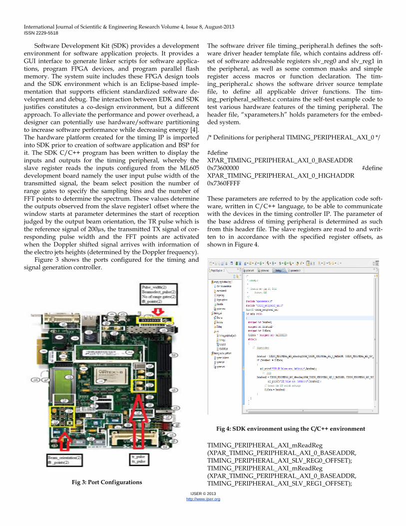
The software driver file timing_peripheral.h defines the soft-ware driver header template file, which contains address off-set of software addressable registers slv_reg0 and slv_reg1 in the peripheral, as well as some common masks and simple register access macros or function declaration. The tim-ing_peripheral.c shows the software driver source template file, to define all applicable driver functions. The tim-ing_peripheral_selftest.c contains the self-test example code to test various hardware features of the timing peripheral. The header file, “xparameters.h” holds parameters for the embed-ded system. /* Definitions for peripheral TIMING_PERIPHERAL_AXI_0 */ #define XPAR_TIMING_PERIPHERAL_AXI_0_BASEADDR 0x73600000 #define XPAR_TIMING_PERIPHERAL_AXI_0_HIGHADDR 0x7360FFFF These parameters are referred to by the application code soft-ware, written in C/C++ language, to be able to communicate with the devices in the timing controller IP. The parameter of the base address of timing peripheral is determined as such from this header file. The slave registers are read to and writ-ten to in accordance with the specified register offsets, as shown in Figure 4.
Fig 4: SDK environment using the C/C++ environment
TIMING_PERIPHERAL_AXI_mReadReg (XPAR_TIMING_PERIPHERAL_AXI_0_BASEADDR, TIMING_PERIPHERAL_AXI_SLV_REG0_OFFSET); TIMING_PERIPHERAL_AXI_mReadReg (XPAR_TIMING_PERIPHERAL_AXI_0_BASEADDR, TIMING_PERIPHERAL_AXI_SLV_REG1_OFFSET);

International Journal of Scientific & Engineering Research Volume 4, Issue 8, August-2013 ISSN 2229-5518
IJSER © 2013
http://www.ijser.org
The software and soft processor core implementation tools are responsible for the parameterization of the soft core and associated peripherals and the implementation of processor buses, memory maps, interrupt structures and required pro-cessor peripherals. The software tools also include traditional compilation, linking, debug and download to the target pro-cessor. The embedded designs on 32 bit processors include OS and any lower-level software required to connect the OS to the hardware to reduce the design time through the board sup-port package. EDK simulation is accomplished by exporting VHDL or Verilog HDL models of the embedded hardware platform design. The models include block RAM (BRAM) memory peripherals that one can initialize with our embedded software ELF file. Verification through behavioural, structural, and timing simulation can be performed at specific points in our design process[6].The timing peripheral IP of the timing control and signal generation controller is set up in the simula-tion environment, added with test bench file, and Xilinx ISim is used to simulate the system. The user logic ports are im-ported into the wave environment and simulated with 10ns corresponding to the processor clock frequency of 100 MHz which is shown in Figure 5.
In order to compare the relative performance of soft pro-cessor cores a common processor benchmark approach must be used. Currently the most common benchmark is the DMIPS (Dhrystone Million Instructions Per Second) benchmark. The DMIPS benchmark is based on running an algorithm on a tar-geted processor core to measure its integer processing capabil-ities within a defined time period.
Fig 5: ISim simulation of the IP timing unit
Xilinx MicroBlaze supports bus clock frequencies up to 150 MHz for which the Virtex FPGA family provides DMIPS up to 150 MHz and Spartan family up to 85 MHz [7].The processor execution of timing peripheral is out of on-chip memory to ensure maximum processor performance. This benchmark
implementation utilizes 2289 LUTs and achieves an operation-al speed of 100 MHz. The benchmark performance achieved is optimized with the use of -1 grade of Virtex6 FPGAs. Debug-ging a design can save weeks design effort and schedule by means of software simulators, real-time software debugger, trace capability and hardware/software logic analyzer trig-gers. Debugging is performed on the evaluation board via a JTAG bus interface. Xilinx‟s ChipScope Pro software provides bus analysis and input-output signals trace capability to sup-port FPGA system-level design evaluation and debug [8]. XPS Debug Configuration Wizard automates hardware and soft-ware debug configuration tasks common to most designs. The ChipScope Pro tools include several utilities that are integrat-ed into a single application; this provides device configura-tion, trigger setup, and trace display for ChipScope Pro cores. The ChipScope AXI Monitor Core, for IBA creates a bit stream containing the ChipScope core and software application. The triggering of IBA has depicted the start of timing peripheral captures of inputs at the address 0x73600000- 0x7360FFFF, as shown in Figure 6.
Fig 6: ChipScop IBA analyser trigger captures
This has been earlier verified at runtime debugging stage when the variables were read in binary format from the disas-sembly window from SDK debugger. Snapshot of the disas-sembly window is seen in the Figure 7.
Fig 7: Disassembly window in SDK

International Journal of Scientific & Engineering Research Volume 4, Issue 8, August-2013 ISSN 2229-5518
IJSER © 2013
http://www.ijser.org
Providing proper match units to trigger the input/output signals gives the user a better provision for a virtual hardware platform capable of providing visual feedback within a con-sole-based window supporting emulating system I/O func-tionality.
The ChipScope ILA analyzer provided from XPS debug wizard provides options to trigger proper match units for the four inputs and outputs, as shown in the Figure 8.The Capture Parameters tab sets the depth of the ILA core. This determines the number of samples that can be stored once the ILA is trig-gered. Data depth settings are adjusted to determine the im-pact of selected parameters (samples) on the resources used by the ILA.
Fig 8: ChipScope ILA triggers for corresponding match units
The implementation of the timing control and signal gen-
eration controller in the soft processor core is beneficial from a system-oriented design approach and the tradeoffs established between hardware and software overshadows its capability to maximize efficiency and performance. Scalability and pro-grammability of the other designed functional blocks of the digital radar receiver can be practically envisaged when each of them is being implemented as IP cores in the MicroBlaze codesign environment, which is adopted as the future work in this area. It is much easier to design, implement, debug and test an FPGA soft processor-based project rather than a standalone block project. The Fast Simplex Link (FSL) inter-faces can further speed up the operation and provide low la-
tencies for the functionality which is again adopted as future work implementation. With latest FPGA hardware design tools, transitioning software bottlenecks from software to hardware is easier since the software C code can be readily adapted into hardware. In general, the future scope of this work focuses building the timing controller on an FSL plat-form and integrating the other functional blocks of the digital radar receiver onto the MicroBlaze codesign environment and applying hardware /software partitioning algorithms to de-crease energy, get the required optimization and increase in efficiency.
4 CONCLUSION
Xilinx MicroBlaze provided by FPGA vendors gives a flexibil-
ity to configure the processors and enable to build FPGA sys-
tems at a quicker and effective pace. By reducing the compo-
nent count in a design, board size and inventory management
can be reduced both of which will save design time and cost.
This implementation of the timing control and signal genera-
tion unit in the soft processor core is benefited from a system-
oriented design approach and the trade-offs established be-
tween Hardware and Software to maximize efficiency and
performance. As future work, Timing unit can be implement-
ed on an FSL Platform which would speed up the operation
and provide low latencies for the functionality. Also, the
codesign environment can be expanded by applying Hard-
ware/ Software partitioning algorithms to decrease energy,
optimization and increased efficiency.
REFERENCES
[1] R.C. Cofer, Ben Harding, “FPGA Soft Processor Design Considera-
tions,” EETIMES, http://www.eetimes.com. 2005.
[2] B.H. Fletcher, “FPGA Embedded Processors: Revealing True System
Performance,” Embedded systems conference San Francisco, pp. 2-18,
ETP-367, 2005.
[3] Yuanbin Wu, Jinwen Li, “The design of Digital Radar Recievers,”
Proc. IEEE National Radar conference, Syracuse, USA pp. 207-210, 1997.
[4] R. Jesman, “MicroBlaze Tutorial Creating a simple Embedded system
and Adding custom Peripherals using Xilinx EDK Software tool ,” Il-
linois Institute of Technology,
http://ecasp.ece.iit.edu/tutorials/microblaze_tutorial.pdf
[5] Roman Lysecky, Frank Vahid, “ A study of the speedups and Com-
petitiveness of FPGA Soft Processor Cores using Dynamic Hard-
ware/ Software Partitioning,” Proc. IEEE Computer Society Conference
on Design, Automation and Testing, Europe, pp. 18-23, 2005.
[6] “MicroBlaze Processor Reference Guide Embedded development
kit,” Xilinx Inc.
[7] “Embedded system tools Reference Manual EDK 12.4,” Xilinx Inc.
[8] “Getting Started with Embedded system development using Micro-
Blaze Processor Spartan-3a FPGAs,” Xilinx Inc.