interfacing the msc8101 upm to an external dual-port...
TRANSCRIPT

Freescale SemiconductorApplication Note
AN2146Rev. 3, 1/2005
CONTENTS
1 UPM and DPRAM Basics .................................. 22 UPM Programming Model .................................32.1 UPM RAM Array ...............................................32.2 Timing Interface Diagrams .................................42.2.1 MSC8101 to DPRAM Single Read Timing .......42.2.2 MSC8101 to DPRAM Single Write Timing ......62.2.3 DPRAM Semaphore Read After Write Timing ..72.2.4 Timing Diagram of Read with BUSY ................ 82.3 RAM Words ......................................................102.3.1 Read ..................................................................132.3.2 Write .................................................................142.3.3 Exception ..........................................................142.4 UPM Registers ..................................................142.5 RAM Array Programming ................................162.6 Memory Controller Bank Registers ..................162.6.1 BRx Register .....................................................162.6.2 ORx Register ....................................................183 UPM Programming Steps ................................. 194 Memory Access ................................................205 Conclusions .......................................................206 References......................................................... 21
Interfacing the MSC8101 UPM to an External Dual-Port SRAMBy Iantha Scheiwe
The MSC8101 is a powerful DSP that integrates the StarCore™ SC140 DSP core, a communications processor module (CPM) for network interfacing, and a system interface unit (SIU). The SIU memory controller includes three user-programmable machines (UPMs). Each UPM controls access to a wide array of memory types, including both synchronous and asynchronous SRAM and DRAM memories.
This application note describes the interface between the MSC8101 UPM and the Cypress CY7C028V dual-port asynchronous SRAM (DPRAM). After a review of UPM and DPRAM basics, it considers the signals interfacing between the two devices as well as the timing diagrams for the interface. The section on the UPM programming model includes programming specifics for the DPRAM interface. After you program the memory controller, you can access the memory in multiple ways from the MSC8101.
© Freescale Semiconductor, Inc., 2001– 2004. All rights reserved.

UPM and DPRAM Basics
1 UPM and DPRAM BasicsThe UPM allows the system designer to program the memory controller signal activity to each 1/2 or 1/4 PowerPC system bus clock cycle so that the UPM can interface to any number of different types of memories. The MSC8101 has three UPMs: UPMA, UPMB, UPMC. UPMC is used on the internal PowerPC local bus to control the interface to internal SRAM from the PowerPC local bus. UPMC is initialized at boot-up so that non-core resources can access the internal SRAM. UPMC is not available for use with external devices. However, UPMA and UPMB are available for access to external devices on the PowerPC system bus.
The Cypress CY7C028V Dual-Port RAM (DPRAM) is an asynchronous SRAM that allows two independent devices to gain access to the SRAM simultaneously through its dual ports. The memory device has two independent sets of address, data, and control lines that allow two devices to access a memory cell. Because the two accessing devices are independent, each can have a unique hardware interface and timing requirement. DPRAM devices include extra functions not found in a standard SRAM that allow one accessing device to lock out a memory cell from the other accessing device if required.
The UPM has six unique signals, PGPL[0–5]. The UPM can use other signals associated with memory accesses as well, including chip selects and byte selects. Figure 1 shows the UPM signals. The PGPL4 signal requires special programming because it can function as an input when it is not required as a PGPL signal.
T1, T2, T3, T4
PGPL0 GPL2PGPL3PGPL4 PGPL5
External Signals Timing Generator (System or Local Bus)
RAM Array
CS Line
Selector
Byte Select
Packaging
CS[0–7,10,11] PBS[0–7]
Current Bank TSIZ[0–3], PS,
32 Bits
64
PGPL1
(Internal Clock assertions associated with each
1/4 System Clock)
Locations(Memory Bank)
External Signals
A[30,31]
Figure 1. UPM Signals
The MSC8101 UPM signal actions are highly programmable. The chip select (CS) and byte select (PBS) signals shown in Figure 1 are programmable to a PowerPC bus 1/4 clock cycle. The General-Purpose Line (PGPL[0–5]) signals are programmable to the 1/2 clock cycle.
Interfacing the MSC8101 UPM to an External Dual-Port SRAM, Rev. 3
2 Freescale Semiconductor

UPM Programming Model
Because the CY7C028V is a dual-ported SRAM, Figure 2 shows how two MSC8101 devices can connect to the SRAM device. The DPRAM uses standard SRAM signals such as chip-select (chip enable), read/write, address, and data lines to define the interface as well as some signals that are required to service the dual ports. Chip-select 4 (CS4) connects to the semaphore (SEM) signal from the DPRAM. Through this signal, the DPRAM controls which device accesses a semaphore latch at a given time. The semaphore latches are memory-mapped separately via the CS4 signal, and the DPRAM device handles semaphore priority. Therefore, the semaphore can keep two DSP devices from over-writing a specific memory location.
CER
R/WR
BUSYR
A[0–15R]
D[0–15R]
SEMR
UBR
LBR
INTR
OER
CS3
PGPL0
PUPMWAIT(GPL4)
A[0–15]
D[0–15]
CS4
PBS1
PBS0
IRQn
MSC8101RCY7C028VCEL
R/WL
BUSYL
A[0–15L]
D[0–15L]
SEML
UBL
LBL
INTL
OEL
CS3
PGPL0
(GPL4)PUPMWAIT
A[0–15]
D[0–15]
CS4
PBS1
PBS0
IRQn
MSC8101L
Figure 2. Dual MSC8101 UPM to CY7C028V DPRAM Signal Interface
The PUPMWAIT signal is the UPM PGPL4 signal that allows an external device to freeze the external signals until the PUPMWAIT signal is released (or the system bus reaches a time-out condition). Therefore, the DPRAM can assert its BUSY signal and hold the MSC8101 transaction until the memory location is released and the MSC8101 writes to the desired location. Upper byte (UB) and Lower byte (LB) signals on the DPRAM connect to the MSC8101 byte select (PBS[0–1]) signals. Therefore, both 8-bit and 16-bit accesses are possible. The DPRAM can generate an interrupt to the MSC8101 via the IRQ signal.
2 UPM Programming ModelThis section discusses the various modules within the UPM and registers that must be programmed to implement a UPM transaction. Section 3, UPM Programming Steps, on page 19 lists the UPM programming steps.
2.1 UPM RAM ArrayEach UPM has a memory bank designated for programming it. This memory bank is called the UPM RAM array and is not memory-mapped but is instead programmed through a sequence of register writes. Six types of memory accesses can be programmed: single read, burst read, single write, burst write, refresh, and exception. Each access is allotted a designated amount of space within the RAM array. Table 1 lists the starting addresses in the RAM array for each access type. These addresses are used in programming the Machine Mode Register, which is discussed later.
Interfacing the MSC8101 UPM to an External Dual-Port SRAM, Rev. 3
Freescale Semiconductor 3
UPM Programming Model
Table 1. UPM Routine Start Addresses
UPM Routine Routine Start Address
Read single-beat (RSS) 0x00
Read burst (RBS) 0x08
Write single-beat (WSS) 0x18
Write burst (WBS) 0x20
Refresh timer (PTS) 0x30
Exception condition (EXS) 0x3C
Because the DPRAM is an SRAM without burst capabilities, the burst read and burst write access types do not require programming. Also, the refresh access is not required. Section 2.3, RAM Words, on page 10 describes the steps for programming the applicable access types in the RAM array. The RAM array is programmed with RAM words that define signal interface timing at each 1/4 bus clock. Examples of this are given in Section 3, UPM Programming Steps, on page 19.
2.2 Timing Interface DiagramsCreating timing diagrams of the memory interface access types makes the UPM programming procedure easier. Since the UPM signals are programmable to 1/2 and 1/4 clock cycles, it helps to refer to the completed timing diagrams when determining the programming for the access types. Therefore, creating the timing diagrams is the first step in programming the UPM RAM array.1 The MSC8101 PowerPC system bus operates at a maximum speed of 100 MHz. A 15 ns access time DPRAM is specified for this timing analysis. The following diagrams are discussed here:
• Single Read Timing
• Single Write Timing
• Semaphore Read after Write Timing
• Read with BUSY
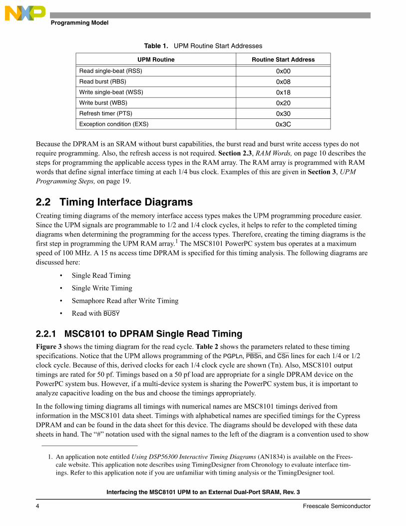
2.2.1 MSC8101 to DPRAM Single Read TimingFigure 3 shows the timing diagram for the read cycle. Table 2 shows the parameters related to these timing specifications. Notice that the UPM allows programming of the PGPLn, PBSn, and CSn lines for each 1/4 or 1/2 clock cycle. Because of this, derived clocks for each 1/4 clock cycle are shown (Tn). Also, MSC8101 output timings are rated for 50 pf. Timings based on a 50 pf load are appropriate for a single DPRAM device on the PowerPC system bus. However, if a multi-device system is sharing the PowerPC system bus, it is important to analyze capacitive loading on the bus and choose the timings appropriately.
In the following timing diagrams all timings with numerical names are MSC8101 timings derived from information in the MSC8101 data sheet. Timings with alphabetical names are specified timings for the Cypress DPRAM and can be found in the data sheet for this device. The diagrams should be developed with these data sheets in hand. The “#” notation used with the signal names to the left of the diagram is a convention used to show
1. An application note entitled Using DSP56300 Interactive Timing Diagrams (AN1834) is available on the Frees-cale website. This application note describes using TimingDesigner from Chronology to evaluate interface tim-ings. Refer to this application note if you are unfamiliar with timing analysis or the TimingDesigner tool.
Interfacing the MSC8101 UPM to an External Dual-Port SRAM, Rev. 3
4 Freescale Semiconductor
UPM Programming Model
low assertion. Therefore, UB# is the same as UB. TimingDesigner does not support overlines on their text, so the “#” notation is used instead. Signal names to the left of the “/” are the DPRAM signal names. Signal names to the right are the associated MSC8101 signal names.
Address
Q(A1)
tHZCEtHZCE
tABEtACE
tAA
tLZCEtLZCE
t34t34
t34t34
t32t32
tOHAt10
t12a
tRCtRC
CLK
T1
T2
T3
T4
Address
UB# or LB#/PBSn#
CE#/CS#
Data
Figure 3. Single Read Cycle Timing
Table 2. Single Read Cycle Timing Parameters
Row Name Min Max Comment
1 V DSP_Name Freescale MSC8101 Digital Signal Processor
2 V MEMORY_Name Cypress CY7C028V Dual-Port Static RAM 64kx16, 15ns
3 V Doc_Reference1 MSC8101 Advance Information, Rev 0.5
4 V Doc_Reference2 Preliminary CY7C027V/028V Data Sheet
5 V Mode_Description UPM Single Read to Dual-Port SRAM, 15ns access time
12 C tRC 15 Read Cycle Time
13 D tLZCE 3 CE low to low Z
14 D tLZCE 3 CE low to low Z
15 G tOHA 3 Output hold from address change
16 D tAA 15 Address to data valid
17 D tACE 15 CE low to data valid
18 D tABE 15 Byte enable access time
19 D tHZCE 10 CE high to high Z
20 D tHZCE 10 CE high to high Z
Interfacing the MSC8101 UPM to an External Dual-Port SRAM, Rev. 3
Freescale Semiconductor 5
UPM Programming Model
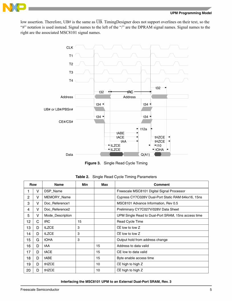
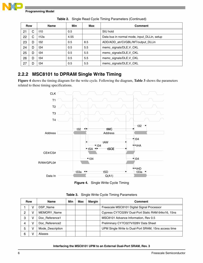
2.2.2 MSC8101 to DPRAM Single Write TimingFigure 4 shows the timing diagram for the write cycle. Following the diagram, Table 3 shows the parameters related to these timing specifications.
Address
Q(A1)t33at33a
t34t34
t34
t34
t32t32
tHDtSD
tHAtSCE
tAW
tSA tSCE
tWCtWC
CLK
T1
T2
T3
T4
Address
CE#/CS#
R/W#/GPL0#
Data In
Figure 4. Single Write Cycle Timing
21 C t10 0.5 SIU hold
22 C t12a 4.55 Data bus in normal mode, input_DLLin, setup
23 D t32 0.5 8.5 ADD/ADD_atr/CI/GBL/WT/output_DLLin
24 D t34 0.5 5.5 memc_signals/DLE,V_CKL
25 D t34 0.5 5.5 memc_signals/DLE,V_CKL
26 D t34 0.5 5.5 memc_signals/DLE,V_CKL
27 D t34 0.5 5.5 memc_signals/DLE,V_CKL
Table 3. Single Write Cycle Timing Parameters
Row Name Min Max Margin Comment
1 V DSP_Name Freescale MSC8101 Digital Signal Processor
2 V MEMORY_Name Cypress CY7C028V Dual-Port Static RAM 64kx16, 15ns
3 V Doc_Reference1 MSC8101 Advance Information, Rev 0.5
4 V Doc_Reference2 Preliminary CY7C027V/028V Data Sheet
5 V Mode_Description UPM Single Write to Dual-Port SRAM, 15ns access time
6 V Aliases
Table 2. Single Read Cycle Timing Parameters (Continued)
Row Name Min Max Comment
Interfacing the MSC8101 UPM to an External Dual-Port SRAM, Rev. 3
6 Freescale Semiconductor

UPM Programming Model
2.2.3 DPRAM Semaphore Read After Write TimingFigure 5 shows the timing diagram for the semaphore read after write cycle. Following the diagram, Table 4 shows the parameters related to these timing specifications.
Address Address
DATAin Valid DATAout VALID
t34t34
tOHA
tSAA
t33at33a
t34t34t34t34
t32t32t32
tPWEtPWE
t10
t12atACEtHDtSD
tSWRDtSOP
tSWRDtSOP
tHA
tSCEtAW
tSA tSCE
CLK
T1
T2
T3
T4
Address
SEM#/CS#
Data
R/W#/PGPL#
Figure 5. Semaphore Read After Write Timing
Notice that this is a chip-select controlled write so it varies slightly from the associated diagram shown in the CY7C028V data sheet.
12 C tWC 15 <17,> Write Cycle Time
13 C tAW 12 <15,> Address valid to write end
14 C tSCE 12 <8,> Write pulse width
15 C tSA 0 <2,> Address set-up to write start
16 C tSD 10 <17,> Data set-up to write end
17 C tHD 0 <0,> Data hold from write end
18 C tHA 0 <0,> Address hold from write end
19 D t32 0.5 8.5 ADD/ADD_atr/CI/GBL/WT/output_DLLin
20 D t34 0.5 5.5 memc_signals/DLE,V_CKL
21 D t33a 0.5 8.5 Data bu, output_DLLin s
22 D t34 0.5 5.5 memc_signals/DLE,V_CKL
23 D t34 0.5 5.5 memc_signals/DLE,V_CKL
Table 3. Single Write Cycle Timing Parameters (Continued)
Row Name Min Max Margin Comment
Interfacing the MSC8101 UPM to an External Dual-Port SRAM, Rev. 3
Freescale Semiconductor 7

UPM Programming Model
Table 4. Semaphore Read After Write Timing Parameters
Row Name Min Max Margin Comment
1 V DSP_Name Freescale MSC8101 Digital Signal Processor
2 V MEMORY_Name Cypress CY7C028V Dual-Port Static RAM 64kx16, 15ns
3 V Doc_Reference1 MSC8101 Advance Information, Rev 0.5
4 V Doc_Reference2 Preliminary CY7C027V/028V Data Sheet
5 V Mode_Description UPM, Semaphore Read after Write timing, 15ns access time
12 C tAW 12 <15,> Address valid to write end
13 C tSCE 12 <8,> CE# low to write end
14 C tSD 10 <17,> Data set-up to write end
15 C tHA 0 <0,> Address hold from write end
16 C tPWE 12 <18,> Write pulse width
17 C tHD 0 <0,> Data hold from write end
18 C tSOP 10 <5,> SEM flag update pulse (OE or SEM)
19 C tSWRD 5 <10,> SEM flag write to read time
20 C tACE 15 <,7> CE low to data valid
21 C tSA 0 <2,> Address set-up to write start
22 D tOHA 3 Output hold from address change
23 D tSAA 15 SEM address access time
24 C t10 0.5 <3,> SIU hold
25 C t12a 4.55 <1.95,> Data bus in normal mode, input_DLLin, setup
26 D t32 0.5 8.5 ADD/ADD_atr/CI/GBL/WT/output_DLLin
27 D t33a 0.5 8.5 Data bu, output_DLLin s
28 D t34 0.5 5.5 memc_signals/DLE,V_CKL
29 D t34 0.5 5.5 memc_signals/DLE,V_CKL
30 D t34 0.5 5.5 memc_signals/DLE,V_CKL
31 D t34 0.5 5.5 memc_signals/DLE,V_CKL
32 D t34 0.5 5.5 memc_signals/DLE,V_CKL
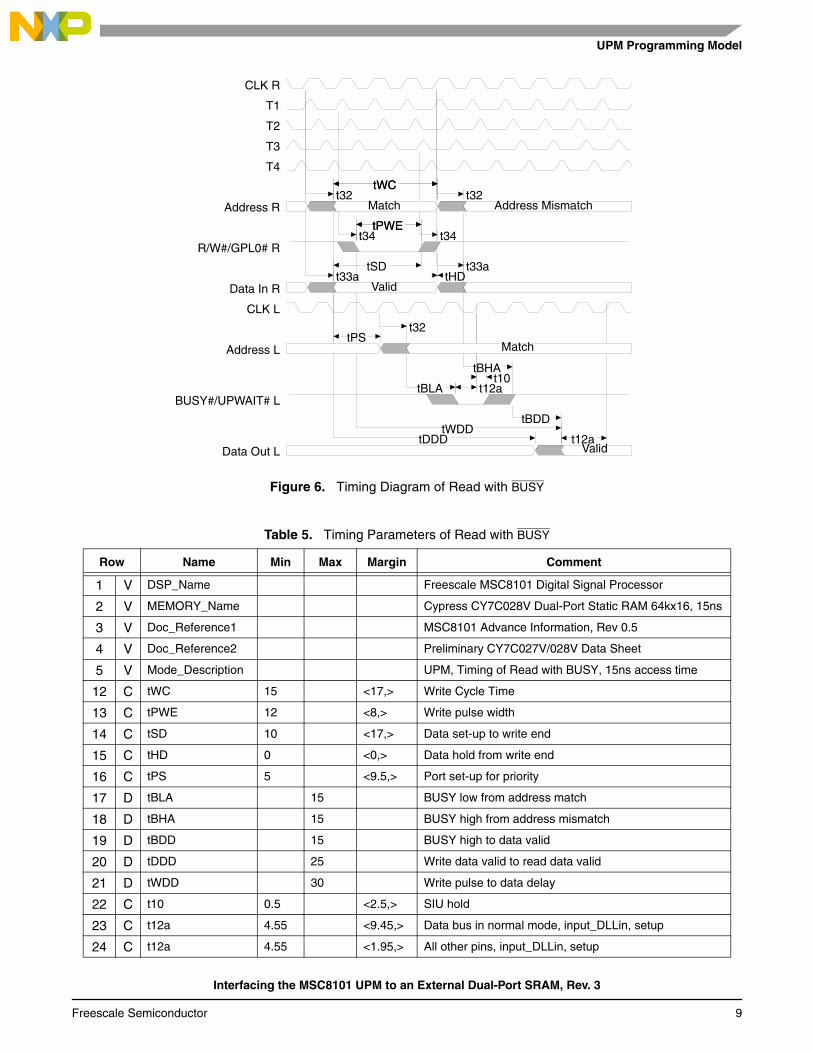
2.2.4 Timing Diagram of Read with BUSYThe DPRAM BUSY signal connects to the MSC8101 PUPMWAIT signal, which is sampled on the falling edge of the MSC8101 bus clock signal. To enable PUPMWAIT, set the Machine Mode Register bit 13, MxMR[13] and set UPM RAM words, bits 18 and 19, to 1. Setting bit 18 directs the MSC8101 to sample the data bus at the rising edge of T3. Setting bit 19 directs the MSC8101 to freeze an external signal logical value if the PUPMWAIT signal is detected. Figure 6 shows the timing diagram for the read cycle with BUSY. Table 5 shows the parameters related to these timing specifications.
Interfacing the MSC8101 UPM to an External Dual-Port SRAM, Rev. 3
8 Freescale Semiconductor
UPM Programming Model
Match Address Mismatch
Valid
Match
Valid
tWDDtDDD
tBDD
tBHA
tBLA
t32
t33at33a
t34t34
t32t32
t12a
t10t12a
tPS
tHDtSD
tPWEtPWE
tWCtWC
CLK R
T1
T2
T3
T4
Address R
R/W#/GPL0# R
Data In R
CLK L
Address L
BUSY#/UPWAIT# L
Data Out L
Figure 6. Timing Diagram of Read with BUSY
Table 5. Timing Parameters of Read with BUSY
Row Name Min Max Margin Comment
1 V DSP_Name Freescale MSC8101 Digital Signal Processor
2 V MEMORY_Name Cypress CY7C028V Dual-Port Static RAM 64kx16, 15ns
3 V Doc_Reference1 MSC8101 Advance Information, Rev 0.5
4 V Doc_Reference2 Preliminary CY7C027V/028V Data Sheet
5 V Mode_Description UPM, Timing of Read with BUSY, 15ns access time
12 C tWC 15 <17,> Write Cycle Time
13 C tPWE 12 <8,> Write pulse width
14 C tSD 10 <17,> Data set-up to write end
15 C tHD 0 <0,> Data hold from write end
16 C tPS 5 <9.5,> Port set-up for priority
17 D tBLA 15 BUSY low from address match
18 D tBHA 15 BUSY high from address mismatch
19 D tBDD 15 BUSY high to data valid
20 D tDDD 25 Write data valid to read data valid
21 D tWDD 30 Write pulse to data delay
22 C t10 0.5 <2.5,> SIU hold
23 C t12a 4.55 <9.45,> Data bus in normal mode, input_DLLin, setup
24 C t12a 4.55 <1.95,> All other pins, input_DLLin, setup
Interfacing the MSC8101 UPM to an External Dual-Port SRAM, Rev. 3
Freescale Semiconductor 9

UPM Programming Model
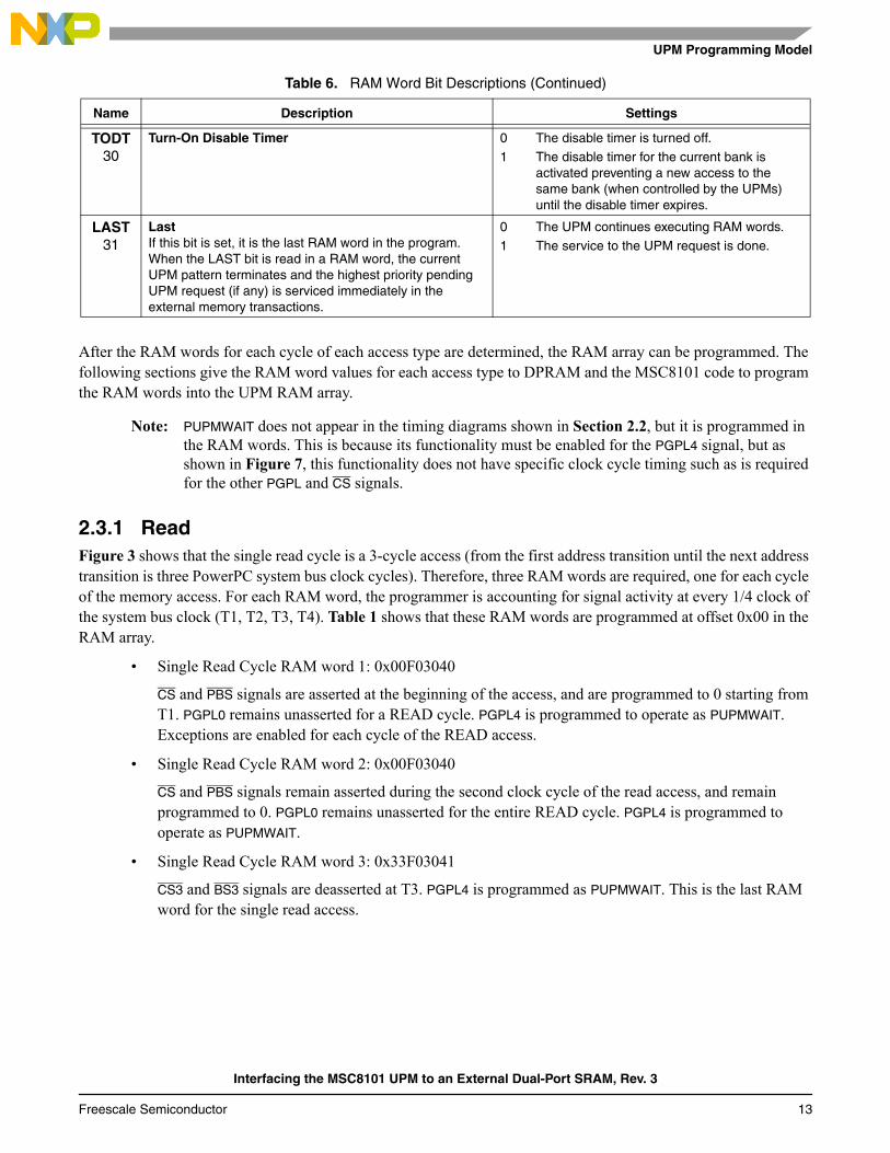
2.3 RAM WordsOnce the timing diagrams for each access type are defined, the UPM signals can be programmed based on those diagrams. The timing for each signal is defined by the RAM word for each cycle of the access. The RAM word, shown in Figure 7, is a 32-bit microinstruction stored in one of 64 locations in the RAM array. It specifies timing for signals controlled by the UPM.
Figure 7. RAM Word
Bit 0 1 2 3 4 5 6 7 8 9 10 11 12 13 14 15
CST1 CST2 CST3 CST4 BST1 BST2 BST3 BST4 G0L G0H G1T1 G1T3 G2T1 G2T3
Bit 16
17 18 19 20 21 22 23 24 25 26 27 28 29 30 31
G3T1 G3T3 G4T1/DLT3
G4T3/WAEN
G5T1 G5T3 REDO LOOP EXEN AMX NA UTA TODT LAST
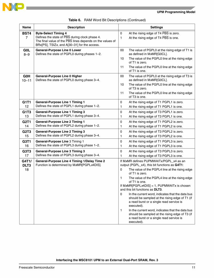
Table 6 describes the RAM word fields.
25 D t32 0.5 8.5 ADD/ADD_atr/CI/GBL/WT/output_DLLin
26 D t32 0.5 8.5 ADD/ADD_atr/CI/GBL/WT/output_DLLin
27 D t33a 0.5 8.5 Data bu, output_DLLin s
28 D t34 0.5 5.5 memc_signals/DLE,V_CKL
29 D t34 0.5 5.5 memc_signals/DLE,V_CKL
Table 6. RAM Word Bit Descriptions
Name Description Settings
CST10
Chip-Select Timing 1Defines the state of CS during clock phase 1.
0 At the rising edge of T1 CS is zero.
1 At the rising edge of T1 CS is one.
CST21
Chip-Select Timing 2Defines the state of CS during clock phase 2.
0 At the rising edge of T2 CS is zero.
1 At the rising edge of T2 CS is one.
CST32
Chip-Select Timing 3Defines the state of CS during clock phase 3.
0 At the rising edge of T3 CS is zero.1 At the rising edge of T3 CS is one.
CST43
Chip-Select Timing 4Defines the state of CS during clock phase 4.
0 At the rising edge of T4 CS is zero.
1 At the rising edge of T4 CS is one.
BST14
Byte-Select Timing 1Defines the state of PBS during clock phase 1. The final value of the PBS lines depends on the values of BRx[PS], the TSIZ lines, and A[30–31] for the access.
0 At the rising edge of T1 PBS is zero.
1 At the rising edge of T1 PBS is one.
BST25
Byte-Select Timing 2Defines the state of PBS during clock phase 2.The final value of the PBS lines depends on the values of BRx[PS], TSIZx, and A[30–31] for the access.
0 At the rising edge of T2 PBS is zero.
1 At the rising edge of T2 PBS is one.
BST36
Byte-Select Timing 3 Defines the state of PBS during clock phase 3.The final value of the PBS lines depends on the values of BRx[PS], TSIZx, and A[30–31] for the access.
0 At the rising edge of T3 PBS is zero.
1 At the rising edge of T3 PBS is one.
Table 5. Timing Parameters of Read with BUSY (Continued)
Row Name Min Max Margin Comment
Interfacing the MSC8101 UPM to an External Dual-Port SRAM, Rev. 3
10 Freescale Semiconductor
UPM Programming Model
BST47
Byte-Select Timing 4Defines the state of PBS during clock phase 4.The final value of the PBS lines depends on the values of BRx[PS], TSIZx, and A[30–31] for the access.
0 At the rising edge of T4 PBS is zero.
1 At the rising edge of T4 PBS is one.
G0L8–9
General-Purpose Line 0 LowerDefines the state of PGPL0 during phases 1–2.
00 The value of PGPL0 at the rising edge of T1 is as defined in MxMR[G0CL].
10 The value of the PGPL0 line at the rising edge of T1 is zero.
11 The value of the PGPL0 line at the rising edge of T1 is one.
G0H10–11
General-Purpose Line 0 HigherDefines the state of PGPL0 during phase 3–4.
00 The value of PGPL0 at the rising edge of T3 is as defined in MxMR[G0CL].
10 The value of the PGPL0 line at the rising edge of T3 is zero.
11 The value of the PGPL0 line at the rising edge of T3 is one.
G1T112
General-Purpose Line 1 Timing 1Defines the state of PGPL1 during phase 1–2.
0 At the rising edge of T1 PGPL1 is zero.
1 At the rising edge of T1 PGPL1 is one.
G1T313
General-Purpose Line 1 Timing 3Defines the state of PGPL1 during phase 3–4.
0 At the rising edge of T3 PGPL1 is zero.1 At the rising edge of T3 PGPL1 is one.
G2T114
General-Purpose Line 2 Timing 1Defines the state of PGPL2 during phase 1–2.
0 At the rising edge of T1 PGPL2 is zero.
1 At the rising edge of T1 PGPL2 is one.
G2T315
General-Purpose Line 2 Timing 3Defines the state of PGPL2 during phase 3–4.
0 At the rising edge of T3 PGPL2 is zero.
1 At the rising edge of T3 PGPL2 is one.
G3T116
General-Purpose Line 3 Timing 1Defines the state of PGPL3 during phase 1–2.
0 At the rising edge of T1 PGPL3 is zero.1 At the rising edge of T1 PGPL3 is one.
G3T317
General-Purpose Line 3 Timing 3Defines the state of PGPL3 during phase 3–4.
0 At the rising edge of T3 PGPL3 is zero.
1 At the rising edge of T3 PGPL3 is one.
G4T1/DLT3
18
General-Purpose Line 4 Timing 1/Delay Time 2 Function is determined by MxMR[PGPLx4DIS].
If MxMR defines PUPMWAITx/PGPL_x4 as an output (PGPL_x4), this bit functions as G4T1:
0 The value of the PGPL4 line at the rising edge of T1 is zero.
1 The value of the PGPL4 line at the rising edge of T1 is one.
If MxMR[PGPLx4DIS] = 1, PUPMWAITx is chosen and this bit functions as DLT3.
0 In the current word, indicates that the data bus should be sampled at the rising edge of T1 (if a read burst or a single read service is executed).
1 In the current word, indicates that the data bus should be sampled at the rising edge of T3 (if a read burst or a single read service is executed).
Table 6. RAM Word Bit Descriptions (Continued)
Name Description Settings
Interfacing the MSC8101 UPM to an External Dual-Port SRAM, Rev. 3
Freescale Semiconductor 11

UPM Programming Model
G4T3/WAEN
19
General-Purpose Line 4 Timing 3/Wait EnableFunction depends on the value of MxMR[PGPLx4DIS].
If MxMR[PGPLx4DIS] = 0, G4T3 is selected.
0 The value of the PGPL4 line at the rising edge of T3 is zero.
1 The value of the PGPL4 line at the rising edge of T3 is one.
If MxMR[PGPLx4DIS] = 1, WAEN is selected.
0 The PUPMWAITx function is disabled.1 A freeze in the external signals logical value
occurs if the external WAIT signal is asserted. This condition lasts until WAIT is deasserted.
G5T120
General-Purpose Line 5 Timing 1Defines the state of PGPL5 during phase 1–2.
0 At the rising edge of T1 PGPL5 is zero.
1 At the rising edge of T1 PGPL5 is one.
G5T321
General-Purpose Line 5 Timing 3Defines the state of PGPL5 during phase 3–4.
0 At the rising edge of T3 PGPL5 is zero.1 At the rising edge of T3 PGPL5 is one.
REDO22–23
Redo Current RAM Word 00 Normal operation.
01 The current RAM word is executed twice.
10 The current RAM word is executed three times.
11 The current RAM word is executed four times.
LOOP24
LoopThe first RAM word in the RAM array where LOOP is one is recognized as the loop start word. The next RAM word where LOOP is one is the loop end word. RAM words between the start and end are defined as the loop. The number of times the UPM executes this loop is defined in the corresponding loop field of the MxMR.
0 The current RAM word is not the loop start word or loop end word.
1 The current RAM word is the start or end of a loop.
EXEN25
Exception Enable 0 The UPM continues executing the remaining RAM words.
1 The current RAM word allows a branch to the exception pattern after the current cycle if an exception condition is detected.
AMX26–27
Address MultiplexingDetermines the source of A[0–31] at the rising edge of T1 (single-MCS8101 mode only).
00 A[0–31] is the non-multiplexed address. For example, column address.
01 Reserved.
10 A[0–31] is the address requested by the internal master multiplexed according to MxMR[AMx]. For example, row address.
11 A[0–31] is the contents of MAR. Used, for example, during SDRAM mode initialization.
NA28
Next AddressDetermines when the address is incremented during a burst access. The value of NA is relevant only when the UPM serves a burst-read or burst-write request. NA is reserved under other patterns.
0 The address increment function is disabled.1 The address is incremented in the next cycle.
UTA29
UPM Transfer AcknowledgeIndicates assertion of PSDVAL, sampled by the bus interface in the current cycle.
0 PSDVAL is not asserted in the current cycle.
1 PSDVAL is asserted in the current cycle.
Table 6. RAM Word Bit Descriptions (Continued)
Name Description Settings
Interfacing the MSC8101 UPM to an External Dual-Port SRAM, Rev. 3
12 Freescale Semiconductor
UPM Programming Model
After the RAM words for each cycle of each access type are determined, the RAM array can be programmed. The following sections give the RAM word values for each access type to DPRAM and the MSC8101 code to program the RAM words into the UPM RAM array.
Note: PUPMWAIT does not appear in the timing diagrams shown in Section 2.2, but it is programmed in the RAM words. This is because its functionality must be enabled for the PGPL4 signal, but as shown in Figure 7, this functionality does not have specific clock cycle timing such as is required for the other PGPL and CS signals.
2.3.1 Read Figure 3 shows that the single read cycle is a 3-cycle access (from the first address transition until the next address transition is three PowerPC system bus clock cycles). Therefore, three RAM words are required, one for each cycle of the memory access. For each RAM word, the programmer is accounting for signal activity at every 1/4 clock of the system bus clock (T1, T2, T3, T4). Table 1 shows that these RAM words are programmed at offset 0x00 in the RAM array.
• Single Read Cycle RAM word 1: 0x00F03040
CS and PBS signals are asserted at the beginning of the access, and are programmed to 0 starting from T1. PGPL0 remains unasserted for a READ cycle. PGPL4 is programmed to operate as PUPMWAIT. Exceptions are enabled for each cycle of the READ access.
• Single Read Cycle RAM word 2: 0x00F03040
CS and PBS signals remain asserted during the second clock cycle of the read access, and remain programmed to 0. PGPL0 remains unasserted for the entire READ cycle. PGPL4 is programmed to operate as PUPMWAIT.
• Single Read Cycle RAM word 3: 0x33F03041
CS3 and BS3 signals are deasserted at T3. PGPL4 is programmed as PUPMWAIT. This is the last RAM word for the single read access.
TODT30
Turn-On Disable Timer 0 The disable timer is turned off.
1 The disable timer for the current bank is activated preventing a new access to the same bank (when controlled by the UPMs) until the disable timer expires.
LAST31
LastIf this bit is set, it is the last RAM word in the program. When the LAST bit is read in a RAM word, the current UPM pattern terminates and the highest priority pending UPM request (if any) is serviced immediately in the external memory transactions.
0 The UPM continues executing RAM words.
1 The service to the UPM request is done.
Table 6. RAM Word Bit Descriptions (Continued)
Name Description Settings
Interfacing the MSC8101 UPM to an External Dual-Port SRAM, Rev. 3
Freescale Semiconductor 13

UPM Programming Model
2.3.2 WriteFigure 4 shows the timing interface for the single write. The single write access is a 4 cycle access, so four RAM words are required to define the write interface. Table 1 shows that these RAM words are programmed at offset 0x18 in the RAM array.
• Single write cycle RAM word 1: 0xEEE03040
Program CS3, PBS3, and PGPL0 (R/W) signals to remain unasserted until T3. PGPL4 is programmed as PUPMWAIT.
• Single write cycle RAM word 2: 0x00A03040
Signals remain asserted throughout second cycle of access. PGPL4 still acts as PUPMWAIT.
• Single write cycle RAM word 3: 0x00A03040
Same as previous RAM word.
• Single write cycle RAM word 4: 0x33B03041
CS3, PBS3, and PGPLO become unasserted at T3. PGPL4 acts as PUPMWAIT. This is the last RAM word for the single write access.
2.3.3 ExceptionAn exception access can be programmed, depending on the requirements for the memory interface. Table shows that these RAM words are programmed at offset 0x3C in the RAM array.
• Exception cycle RAM word 1: 0xFF000001. Deassert CS3 and PBS3 signals and end access.
2.4 UPM RegistersBesides the RAM words programmed in the UPM RAM array and BR and OR registers, two other UPM registers, the Memory Data Register (MDR) and the Machine x Mode Registers (MxMR) are used when the UPM is programmed. The MDR contains data written to or read from the RAM array for UPM READ or WRITE commands. MDR must be set up before a WRITE command is issued to the UPM. The MDR is a 32-bit register that holds the memory data information. Data to be written into the RAM array when a WRITE command is supplied to the UPM should be placed in the MDR before the write access is initiated.
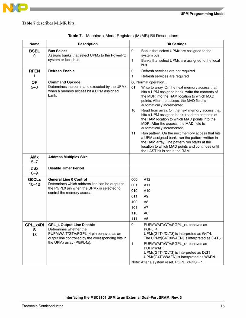
The MxMR, shown in Figure 8, contain the configuration for the UPMs. The configuration includes selecting the bus that the memory is assigned to, specifying whether refresh is required, and specifying the multiplex information used primarily for access to DRAMs. Also, this register defines how many times looping RAM words should be repeated. When programming the RAM array, you inform the UPM that it is being programmed at a given RAM array address by setting the Command Opcode bits (OP) to the RAM array access function and the Machine Address (MAD) bits to the address in the RAM array being accessed.
Figure 8. Machine x Mode Registers (MxMR)
Bit 0 1 2 3 4 5 6 7 8 9 10 11 12 13 14 15
BSEL RFEN OP — AMx DSx G0CLx GPL_x4DIS RLFx
Bit 16 17 18 19 20 21 22 23 24 25 26 27 28 29 30 31
RLFx WLFx TLFx MAD
Interfacing the MSC8101 UPM to an External Dual-Port SRAM, Rev. 3
14 Freescale Semiconductor
UPM Programming Model
Table 7 describes MxMR bits.
Table 7. Machine x Mode Registers (MxMR) Bit Descriptions
Name Description Bit Settings
BSEL0
Bus SelectAssigns banks that select UPMx to the PowerPC system or local bus.
0 Banks that select UPMx are assigned to the system bus.
1 Banks that select UPMx are assigned to the local bus.
RFEN1
Refresh Enable 0 Refresh services are not required
1 Refresh services are required
OP2–3
Command OpcodeDetermines the command executed by the UPMx when a memory access hit a UPM assigned bank.
00 Normal operation.01 Write to array. On the next memory access that
hits a UPM assigned bank, write the contents of the MDR into the RAM location to which MAD points. After the access, the MAD field is automatically incremented.
10 Read from array. On the next memory access that hits a UPM assigned bank, read the contents of the RAM location to which MAD points into the MDR. After the access, the MAD field is automatically incremented
11 Run pattern. On the next memory access that hits a UPM assigned bank, run the pattern written in the RAM array. The pattern run starts at the location to which MAD points and continues until the LAST bit is set in the RAM.
AMx5–7
Address Multiplex Size
DSx8–9
Disable Timer Period
G0CLx10–12
General Line 0 ControlDetermines which address line can be output to the PGPL0 pin when the UPMx is selected to control the memory access.
000 A12
001 A11
010 A10
011 A9
100 A8
101 A7
110 A6
111 A5
GPL_x4DIS13
GPL_4 Output Line DisableDetermines whether the PUPMWAIT/GTA/PGPL_4 pin behaves as an output line controlled by the corresponding bits in the UPMx array (PGPL4x).
0 PUPMWAIT/GTA/PGPL_x4 behaves as PGPL_4. UPMx[G4T4/DLT3] is interpreted as G4T4. The UPMx[G4T3/WAEN] is interpreted as G4T3.
1 PUPMWAIT/GTA/PGPL_x4 behaves as PUPMWAIT. UPMx[G4T4/DLT3] is interpreted as DLT3. UPMx[G4T3/WAEN] is interpreted as WAEN.
Note: After a system reset, PGPL_x4DIS = 1.
Interfacing the MSC8101 UPM to an External Dual-Port SRAM, Rev. 3
Freescale Semiconductor 15

UPM Programming Model
2.5 RAM Array Programming When the MxMR register is programmed to “write to array” mode (MxMR[OP]=01), any access to the memory space defined by the Base Register (BR) and Option Register (OR) causes the data currently residing the Memory Data Register (MDR) to be placed in the UPM RAM array at the address defined by the MxMR:MAD bits. Section 3, UPM Programming Steps, on page 19 details the code required for each step of programming the MSC8101 for a UPM interface to DPRAM.
2.6 Memory Controller Bank RegistersThe Option Register (OR) and Base Register (BR) define the memory address in the MSC8101 memory map and general memory controller functions.
2.6.1 BRx RegisterThe base registers (BR0–7, 10, 11) contain the base address and address types that the memory controller uses to compare the address bus value with the current address accessed. Notice that there are no BR8 and BR9 registers. These two banks are reserved on the MSC8101. Each register also includes a memory attribute and selects the machine for memory operation handling. Figure 9 shows the BRx register format.
RLFx14–17
Read Loop FieldDetermines the number of times a loop defined in the UPMx executes for a burst- or single-beat read pattern or when MxMR[OP] = 11 (RUN command)
0001 The loop is executed 1 time
0010 The loop is executed 2 times
...
1111 The loop is executed 15 times
0000 The loop is executed 16 times
WLFx18–21
Write Loop FieldDetermines the number of times a loop defined in the UPMx executes for a burst- or single-beat write pattern.
0001 The loop is executed 1 time
0010 The loop is executed 2 times
...
1111 The loop is executed 15 times
0000 The loop is executed 16 times
TLFx22–25
Refresh Loop FieldDetermines the number of times a loop defined in the UPMx executes for a refresh service pattern.
0001 The loop is executed 1 time
0010 The loop is executed 2 times
...
1111 The loop is executed 15 times
0000 The loop is executed 16 times
MAD26–31
Machine AddressRAM address pointer for the command executed. This field is incremented by 1 each time the UPM is accessed and the OP field is set to WRITE or READ.
Table 7. Machine x Mode Registers (MxMR) Bit Descriptions (Continued)
Name Description Bit Settings
Interfacing the MSC8101 UPM to an External Dual-Port SRAM, Rev. 3
16 Freescale Semiconductor

UPM Programming Model
Figure 9. Base Registers (BRx)
Bit 0 1 2 3 4 5 6 7 8 9 10 11 12 13 14 15
BA
Bit 16 17 18 19 20 21 22 23 24 25 26 27 28 29 30 31
BA — PS DECC WP MS EMEMC ATOM DR V
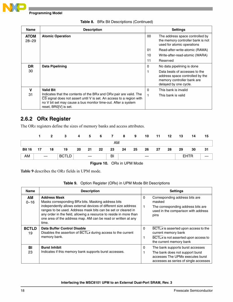
Table 8 describes BRx fields.
Table 8. BRx Bit Descriptions
Name Description Settings
BA0–16
Base AddressThe upper 17 bits of each base address register are compared to the address on the address bus to determine if the bus master is accessing a memory bank controlled by the memory controller. BRx[BA] is used with ORx[BSIZE].
PS19–20
Port SizeSpecifies the port size of this memory region.
01 8-bit
10 16-bit
11 32-bit
00 64-bit
DECC21–22
Data Error Correction and CheckingSpecifies the method for data error checking and correction.
00 Data errors checking disabled
01 Normal parity checking
10 Read-modify-write parity checking
11 ECC correction and checking
WP23
Write ProtectCan restrict write accesses within the address range of a BR. An attempt to write to this address range while WP = 1 can cause TEA to be asserted by the bus monitor logic (if enabled) which terminates the cycle. When WP is set, the memory controller does not assert CSx and PSDVAL on write cycles to this memory bank. TESCR1[WP] or L_TESCR1[WP] is set if a write to this memory bank is attempted
0 Read and write accesses are allowed
1 Only read access is allowed
MS24–26
Machine SelectSpecifies machine select for the memory operations handling and assigns the bank to the PowerPC system bus if GPCM or SDRAM are selected. If UPMx is selected, the bus assignment is determined by MxMR[BSEL].
000 GPCM— system bus
001 GPCM—local bus
010 SDRAM— system bus
011 Reserved
100 UPMA
101 UPMB
110 UPMC
111 Reserved
EMEMC27
External MEMC EnableOverrides MSEL and assigns the bank to the PowerPC system bus. When this bit is set, the external memory controller is expected to assert AACK, TA, and PSDVAL.
0 Accesses are handled by the memory controller according to MSEL
1 Accesses are handled by an external memory controller (or other slave) on the system bus
Interfacing the MSC8101 UPM to an External Dual-Port SRAM, Rev. 3
Freescale Semiconductor 17
UPM Programming Model
2.6.2 ORx RegisterThe ORx registers define the sizes of memory banks and access attributes.
Figure 10. ORx in UPM Mode
Bit 0 1 2 3 4 5 6 7 8 9 10 11 12 13 14 15
AM
Bit 16 17 18 19 20 21 22 23 24 25 26 27 28 29 30 31
AM — BCTLD — BI — EHTR —
Table 9 describes the ORx fields in UPM mode.
ATOM28–29
Atomic Operation 00 The address space controlled by the memory controller bank is not used for atomic operations
01 Read-after-write-atomic (RAWA)
10 Write-after-read-atomic (WARA)
11 Reserved
DR30
Data Pipelining 0 No data pipelining is done
1 Data beats of accesses to the address space controlled by the memory controller bank are delayed by one cycle.
V31
Valid BitIndicates that the contents of the BRx and ORx pair are valid. The CS signal does not assert until V is set. An access to a region with no V bit set may cause a bus monitor time-out. After a system reset, BR0[V] is set.
0 This bank is invalid
1 This bank is valid
Table 9. Option Register (ORx) in UPM Mode Bit Descriptions
Name Description Settings
AM0–16
Address MaskMasks corresponding BRx bits. Masking address bits independently allows external devices of different size address ranges to be used. Address mask bits can be set or cleared in any order in the field, allowing a resource to reside in more than one area of the address map. AM can be read or written at any time.
0 Corresponding address bits are masked
1 The corresponding address bits are used in the comparison with address pins
BCTLD19
Data Buffer Control DisableDisables the assertion of BCTLx during access to the current memory bank.
0 BCTLx is asserted upon access to the current memory bank
1 BCTLx is not asserted upon access to the current memory bank
BI23
Burst InhibitIndicates if this memory bank supports burst accesses.
0 The bank supports burst accesses
1 The bank does not support burst accesses The UPMx executes burst accesses as series of single accesses
Table 8. BRx Bit Descriptions (Continued)
Name Description Settings
Interfacing the MSC8101 UPM to an External Dual-Port SRAM, Rev. 3
18 Freescale Semiconductor

UPM Programming Steps
3 UPM Programming StepsEach step in programming the UPM includes accompanying example code for reference:
1. Evaluate interface timings to determine if the UPM is required. See Section 2.2 for reference. These diagrams include single read and single write as described in this document, but they may also include burst read and write as well as read-after-write diagrams.
2. Program BRx and ORx for the chosen UPM operation at the desired memory address.IMM->memc_regs[3].br = 0xC00018A1; /*place at 0xC0000000,
port size = 32 bits, UPMB, valid bank*/IMM->memc_regs[3].or = 0xFFFF9004; /*64k device, does not
support burst */
3. Determine RAM word settings for each type of access required (single read, burst read, and so on).Single Write Access RAM Word 1 = 0xEEE03040CS and PBS low at T4, PGPL0 low at T3, sample data bus at rising edge of T3 Single Write Access RAM Word 2 = 0x00A03040CS, PBS, and PGPL0 low throughout cycle, sample bus at rising edge of T3Single Write Access RAM Word 3 = 0x00A03040 Single Write Access RAM Word 4 = 0x33B03041CS, PBS, and PGPL0 high at T3, sample bus at rising edge of T3, exceptions enabled, last RAM word
4. Program MxMR for the chosen UPM (that is, MAMR for UPMA, MBMR for UPMB). Set the OP bits to 01 for the write operation. Set the Machine Address to the access type address given in Table 1.IMM->memc_mbmr = 0x10004458; /*PowerPC system bus, write */
5. Program the first RAM word (that is, the first cycle of the single write access) into the Memory Data Register (MDR).IMM->memc_mdr = 0xEEE03040; /* first RAM word placed in MDR*/
6. Perform a random move operation to an address within the range specified by BR and OR for the device. This move operation activates the UPM associated with the device, and the data from the MDR is placed into the RAM array at the address specified by the MBMR:MAD bits. The RAM array address automatically increments so it is ready for the next RAM word. mem_ptr = (unsigned long int *)0xC0000000; /*initialize ptr to
beginning of mem*/*mem_ptr = 0xFFFFFFFF; /*move random value to memory space,
RAM word will be written to RAM array */
7. Continue the move operations to the memory space until the entire RAM array is programmed for each access type. Once one access type is complete, be sure to change the MBMR:MAD address to the next access type before initiating the next move to the UPM memory space.*IMM->memc_mdr = 0x00A03040;*mem_ptr = 0xFFFFFFFF; /* move random value to memory space,
EHTR29–30
Extended Hold Time on Read AccessesIndicates how many cycles are inserted between a read access from the current bank and the next access.
00 Normal timing is generated by the memory controller. No additional cycles are inserted
01 One idle clock cycle is inserted
10 Four idle clock cycles are inserted
11 Eight idle clock cycles are inserted
Table 9. Option Register (ORx) in UPM Mode Bit Descriptions
Name Description Settings
Interfacing the MSC8101 UPM to an External Dual-Port SRAM, Rev. 3
Freescale Semiconductor 19
Memory Access
second RAM word is written to RAM array */
IMM->memc_mdr = 0x00A03040;*mem_ptr = 0xFFFFFFFF; /* move random value to memory
space, RAM word will bewritten to RAM array */
IMM->memc_mdr = 0x33B03041;*mem_ptr = 0xFFFFFFFF; /*move random value to memory
space,fourth RAM word is written to RAM array at single write */
8. Program the MBMR:OP to normal operation.*IMM->memc_mbmr = 0x00004440;
Now you can access the memory device as usual.
4 Memory AccessThe SC140 core can access the DPRAM using a move instruction such as those described in Section 3, UPM Programming Steps. This move operation allows the SC140 core to access the external memory directly if needed for either a data save to external memory or a data retrieval from external memory. Also, program code can be placed in external memory, and the SC140 core can execute from external memory. However, accessing external memory is not an efficient use of the SC140 core. Ideally, in DSP applications, the SC140 core is free from memory retrieval and is used for algorithmic processing. The Direct Memory Access Engine (DMA) handles data transfers from external memory to internal memory so that the SC140 core can operate primarily from internal memory, thus improving system efficiency.
DMA access to the Dual-Port SRAM is no different from other types of DMA accesses. Once the DMA controller has access to the bus, the transaction acts as a PowerPC system bus transaction according to the timings shown in Section 2.2. If the DMA channel’s Buffer Descriptor Address (BD_ADDR) value matches the memory controller bank associated with the DPRAM, then the UPM activates the appropriate CS signal. The DMA controller requests access to the bus. The MSC8101 User’s Guide includes a chapter that shows examples of programming the DMA controller for various applications, including transfers from external memory on the PowerPC system bus to internal SRAM on the MSC8101.
A system application may require a data transfer between two devices resident on the PowerPC system bus. If both of these devices have the same port size, the flyby mode of the DMA can be used. Flyby mode does not require the intermediate FIFO step required by a regular DMA channel. Be sure to consider DMA flyby mode if the system requires transfer between memories or other devices on the PowerPC system bus.
A separate DMA engine, SDMA, resides within the CPM portion of the MSC8101. SDMA can initiate data transfers between the Cypress DPRAM discussed in this document and the CPM communication controllers. A system application can use the CPM communication controllers to bring data into the device. If the data does not reside entirely in internal SRAM, SDMA can be used to transfer the data to the Cypress DPRAM on the 60x-compatible system bus until the SC140 core requires it for processing.
5 ConclusionsTo make the most of the UPM strengths, you must understand the programming steps required to initialize the UPM properly. This application note presents the registers and RAM array that must be programmed to operate the UPM and describes the steps required to complete the program. An example illustrates the programming steps. The UPM is a powerful memory interface machine that enables flexible system design.
Interfacing the MSC8101 UPM to an External Dual-Port SRAM, Rev. 3
20 Freescale Semiconductor
References
6 References[1] MSC8101 Reference Manual.[2] Cypress, CY7C028V Datasheet.[3] Cypress, Understanding Asynchronous Dual-Port RAMs.[4] MSC8101 Technical Data sheet (MSC8101)
Interfacing the MSC8101 UPM to an External Dual-Port SRAM, Rev. 3
Freescale Semiconductor 21

References
NOTES:
Interfacing the MSC8101 UPM to an External Dual-Port SRAM, Rev. 3
22 Freescale Semiconductor
References
NOTES:
Interfacing the MSC8101 UPM to an External Dual-Port SRAM, Rev. 3
Freescale Semiconductor 23
AN2146
Information in this document is provided solely to enable system and software implementers to use Freescale Semiconductor products. There are no express or implied copyright licenses granted hereunder to design or fabricate any integrated circuits or integrated circuits based on the information in this document.
Freescale Semiconductor reserves the right to make changes without further notice to any products herein. Freescale Semiconductor makes no warranty, representation or guarantee regarding the suitability of its products for any particular purpose, nor does Freescale Semiconductor assume any liability arising out of the application or use of any product or circuit, and specifically disclaims any and all liability, including without limitation consequential or incidental damages. “Typical” parameters which may be provided in Freescale Semiconductor data sheets and/or specifications can and do vary in different applications and actual performance may vary over time. All operating parameters, including “Typicals” must be validated for each customer application by customer’s technical experts. Freescale Semiconductor does not convey any license under its patent rights nor the rights of others. Freescale Semiconductor products are not designed, intended, or authorized for use as components in systems intended for surgical implant into the body, or other applications intended to support or sustain life, or for any other application in which the failure of the Freescale Semiconductor product could create a situation where personal injury or death may occur. Should Buyer purchase or use Freescale Semiconductor products for any such unintended or unauthorized application, Buyer shall indemnify and hold Freescale Semiconductor and its officers, employees, subsidiaries, affiliates, and distributors harmless against all claims, costs, damages, and expenses, and reasonable attorney fees arising out of, directly or indirectly, any claim of personal injury or death associated with such unintended or unauthorized use, even if such claim alleges that Freescale Semiconductor was negligent regarding the design or manufacture of the part.
Freescale™ and the Freescale logo are trademarks of Freescale Semiconductor, Inc. StarCore is a trademark of StarCore LLC. All other product or service names are the property of their respective owners.
© Freescale Semiconductor, Inc.2001–2004.
How to Reach Us:Home Page:www.freescale.com
E-mail:[email protected]
USA/Europe or Locations not listed:Freescale Semiconductor Technical Information Center, CH3701300 N. Alma School RoadChandler, Arizona 85224+1-800-521-6274 or [email protected]
Europe, Middle East, and Africa:Freescale Halbleiter Deutschland GMBHTechnical Information CenterSchatzbogen 781829 München, Germany+44 1296 380 456 (English)+46 8 52200080 (English)+49 89 92103 559 (German)+33 1 69 35 48 48 (French)[email protected]
Japan:Freescale Semiconductor Japan Ltd. HeadquartersARCO Tower 15F1-8-1, Shimo-Meguro, Meguro-ku,Tokyo 153-0064, Japan0120 191014 or +81 3 5437 [email protected]
Asia/Pacific:Freescale Semiconductor Hong Kong Ltd.Technical Information Center2 Dai King StreetTai Po Industrial EstateTai Po, N.T. Hong Kong+800 2666 8080
For Literature Requests Only:Freescale Semiconductor Literature Distribution CenterP.O. Box 5405Denver, Colorado 802171-800-441-2447 or 303-675-2140Fax: [email protected]
Rev. 31/2005