interface to a hiperface position encoder (rev. a) · position feedback interface module i-v...
TRANSCRIPT

Position Feedback Interface Module
Sin, Cos
TTL
Sin, Cos
SPI
24 V
Option 1Dual ADC with SPI
Option 2Dual analog out
DualADC
Differential Sin and Cos
Comparators
Sin, Cos
Analog
HIPERFACE encoder
Power supplies
Encoder supply: 11 V
5 V3.3 V
Hos
t pro
cess
orH
IPE
RF
AC
E m
aste
r
TIDA-00202
Enc
oder
con
nect
or
Differential Sin and Cos
Differential RS-485
RS-485 transceiver
TxD, RxD
TxEN
TTL
1TIDUB64A–December 2015–Revised March 2016Submit Documentation Feedback
Copyright © 2015–2016, Texas Instruments Incorporated
Interface to a HIPERFACE Position Encoder
TI DesignsInterface to a HIPERFACE Position Encoder
All trademarks are the property of their respective owners.
TI DesignsThis design implements an EMC-compliant industrialhybrid analog and digital interface to a HIPERFACEposition encoder. A 3.3-V supply RS-485 transceiverwith IEC-ESD and IEC-EFT protection is used for thebidirectional parameter channel. For the analog sin/cossignal channel, two options are provided to offerflexibility for connection to processors with and withoutembedded ADC. The first option features a fullydifferential dual 12-bit ADC with SPI output, and thesecond option features a dual differential input with asingle-ended analog output (0 to 3.3 V). The designfeatures an industrial compliant 24-V input with a widerange from 16 to 36 V. The power supply for theencoder can be configured from 7 to 12 V (default11 V) and offers short-circuit protection. A 3.3-V I/Oconnector with analog and logic signals provides aneasy interface to a host processor with HIPERFACEmaster IP core. For quick evaluation, an examplefirmware is available for a C2000™ Piccolo™ MCU tocalculate the absolute angle position and display itthrough virtual COM port.
Design Resources
TIDA-00202 Tool Folder Containing Design FilesSN65HVD72 Product FolderADS7254 Product FolderTHS4531A Product FolderOPA2365 Product FolderTLV3202 Product FolderTPS5401 Product FolderC2000 Piccolo F28069MMCU LaunchPad Tools Folder
ASK Our E2E Experts
space
Design Features• EMC-Compliant Interface to HIPERFACE Position
Encoders With Digital Bidirectional ParameterChannel up to 38400 Baud and Analog Sin/CosChannel With at Least 150-kHz Bandwidth
• 3.3-V Supply Half-Duplex RS-485 Transceiver With12-kV IEC-ESD and 4-kV IEC-EFT
• Dual Signal Path Option for Sine and CosineSignals With Wither Dual 12-bit ADC With SPIOutput or Dual Analog Output (0 to 3.3 V) to OfferFlexibility for Connection to MCU With and WithoutEmbedded ADC
• Host Processor Interface (3.3-V I/O) for EasyConnection to MCU Like C2000 for HIPERFACEMaster
• Example Firmware on C2000 Piccolo MCU toCalculate and Display the Interpolated AbsoluteAngle From HIPERFACE Position Encoders
• Designed to Meet EMC Immunity for ESD, FastTransient Burst, and Surge With Levels Accordingto IEC61800-3
Featured Applications• Servo Drives• Industrial Drives• Factory Automation and Control
space
space

Position Feedback Interface Module
I-V sensingControlPower
ApplicationCommunication
Frequency inverter
HIPERFACE encoder
Shielded twisted pairs cable from 50 to 150 m
Differential Sine and Cosine and RS-485 transceiver
AC motor
Position Feedback Interface Module
Sin, Cos
TTL
Sin, Cos
SPI
24 V
Option 1Dual ADC with SPI
Option 2Dual analog out
DualADC
Differential Sin and Cos
Comparators
Sin, Cos
Analog
Power supplies
Encoder supply: 11 V
5 V3.3 V
Hos
t pro
cess
orH
IPE
RF
AC
E m
aste
r
TIDA-00202
Enc
oder
con
nect
or
Differential Sin and Cos
Differential RS-485
RS-485 transceiver
TxD, RxD
RxEN
TTL
System Description www.ti.com
2 TIDUB64A–December 2015–Revised March 2016Submit Documentation Feedback
Copyright © 2015–2016, Texas Instruments Incorporated
Interface to a HIPERFACE Position Encoder
An IMPORTANT NOTICE at the end of this TI reference design addresses authorized use, intellectual property matters and otherimportant disclaimers and information.
1 System DescriptionThis TI Design implements an industrial temperature and EMC-compliant interface to a HIPERFACEposition encoder. The major building blocks of this TI Design are the hybrid interface for the bidirectionalparameter channel, a dual-channel option for the analog sine and cosine process data signals, and theHIPERFACE-compliant encoder power supply with an enable signal through MCU.
A simplified system block diagram of a servo drive with a HIPERFACE master interface to a HIPERFACEencoder is shown in Figure 1 with the TI Design represented by the box in light green. To evaluate andtest the TI Design TIDA-00202, a basic HIPERFACE master firmware was implemented on the C2000Piccolo MCU This firmware is only showing basic HIPERFACE functionality for test purposes and providedin binary format.
Figure 1. Simplified Block Diagram of TIDA-00202

www.ti.com System Description
3TIDUB64A–December 2015–Revised March 2016Submit Documentation Feedback
Copyright © 2015–2016, Texas Instruments Incorporated
Interface to a HIPERFACE Position Encoder
The reference design connects to the HIPERFACE encoder through a Sub-D9 connector. The Sub-D9connector has been tested to support cable lengths up to 100 m. For cable specifications, refer to theHIPERFACE standard.
The reference design is powered through a standard 24-V DC rail as typically used in drives. DC/DC buckconverters generate two intermediate rails. These rails are used to generate the point of load 5-V and3.3-V rails to supply the RS-485 transceiver and the analog signal chain, as well as the 11-V rail to supplythe HIPERFACE encoder.
A dual option is provided for the analog process channel to provide flexibility select the processor toimplement the HIPERFACE master. The first option offers an analog signal chain for processors withembedded dual ADC. The second option leverages a dual 12-bit ADC with SPI for processors withoutembedded dual ADC. Both channels can also be used in parallel to for additional redundancy orbandwidth optimization.
A 3.3-V compliant interface is provided to connect to a host processor to run the HIPERFACE masterprotocol as well as the signal processing for the sine and cosine signals.
The host processor interface provides the Data_IN, Data_OUT, and Data_EN signals for the digitalparameter channel, an SPI with dual 12-bit data, and dual analog single-ended signals to support bothprocessors with and without embedded ADCs as well as the quadrature encoded digital signals A and Bfor an incremental up-down counter.
1.1 Introduction to HIPERFACEHIPERFACE is a digital protocol specified and owned by Sick. HIPERFACE is derived from HIghPERformance InterFACE. The key features of the HIPERFACE hybrid interface with reference toHIPERFACE specification from Sick are:• Analog process data channel on which sine and cosine signals are transmitted differentially, with
almost no delay• Bidirectional parameter channel corresponding to the RS-485 specification for transmitting the absolute
position information and various other parameters• Only eight wires• Cable length up to 100 m
1.1.1 HIPERFACE Physical Layer for the Digital InterfaceThe protocol is implemented with a standard UART interface, which can be found on the majority of thehost processors.
As a physical layer, HIPERFACE uses a digital transfer in accordance with EIA-485 (RS-485). ValidRS-485 interface drivers must comply with the conditions in Table 1.
Table 1. HIPERFACE Transceiver Specifications
CHARACTERISTIC VALUETransfer rate 0.6 to 38.4 kBaud (default 9.6 kBaud)Permitted common-mode voltage –7 to 12 VTermination impedance 130-Ω termination with 1k resistor to GND

System Description www.ti.com
4 TIDUB64A–December 2015–Revised March 2016Submit Documentation Feedback
Copyright © 2015–2016, Texas Instruments Incorporated
Interface to a HIPERFACE Position Encoder
1.1.2 HIPERFACE Physical Layer for the Analog Sin/Cos InterfaceIncremental rotary or linear position encoders are used in many applications to measure angular or linearposition and speed. Depending on the application, encoders with TTL/HTL output signals or analogsinusoidal output signals are used. The latter is often referred to as sin/cos encoders. Analog sin/cosincremental encoders enable high-resolution position measurement. The high quality of the sinusoidalincremental signals permits high interpolation factors for digital speed control.
For more details on how to calculate the angle using the sin/cos and TTL signals, see the TIDA-00176 orTIDA-00178 reference design.
As a physical layer, HIPERFACE uses a differential analog sin/cos signal. A valid analog interface mustcomply with the conditions in Table 2.
Table 2. Analog HIPERFACE Signal Chain Specifications
CHARACTERISTIC VALUEMinimum ADC resolution 10 bitADC channel need 2 channelsDifferential signal amplitude (peak-to-peak) 0.9 to 1.1 VPP
Average signal voltage 2.0- to 3.0-V DCSignal bandwidth (3-dB signal amplitude) 0 to 150 kHzOutput load capacity (current) ≥ ±7 mA
1.1.3 HIPERFACE Encoder Supply VoltageMotor feedback systems with HIPERFACE have been developed to operate with a supply voltage of7 to 12 V. The voltage supply is measured at the encoder plug connector. The specification for theHIPERFACE power supply is listed in Table 3.
Table 3. Power Supply Specification
PARAMETER VALUEOperating supply voltage 7 to 12 VOperating current ≤ 250 mA

www.ti.com Key System Specifications
5TIDUB64A–December 2015–Revised March 2016Submit Documentation Feedback
Copyright © 2015–2016, Texas Instruments Incorporated
Interface to a HIPERFACE Position Encoder
2 Key System SpecificationsAs outlined in Section 1, this TI Design realizes an industrial temperature range, EMC-compliant interfaceto HIPERFACE position encoders with differential analog output signals sin/cos, a digital RS-485 UARTinterface, and a 11-V supply voltage. The major building blocks of this TI Design are the dual path analogsignal chain with the low propagation delay comparator block, the RS-485 interface, the powermanagement block, the interfaces to the HIPERFACE encoder, and the interface to a host microcontrollerfor running the HIPERFACE master including digital signal processing and high-resolution positioncalculation.
To evaluate this TI Design with ease, an example firmware is provided for the TMS320F28069MInstaSPIN-MOTION™ LaunchPad™. The TMS320F28069M calculates the high-resolution angle positionfor both signal paths, using both options simultaneously, which are the dual 12-bit ADC through SPI andthe analog output path to the TMS320F28069 internal dual S/H 12-bit ADC. The TMS320F28069M alsoimplements a basic HIPERFACE master to request absolute angle position through the RS-485 interface.A menu is made available through a USB virtual COM port to display the high-resolution interpolatedangle, the absolute angle through the digital parameter channel, and more.
TIDA-00202 features overview:• EMC-compliant interface to HIPERFACE position encoders with digital bidirectional parameter channel
up to 38400 baud and analog sin/cos channel with at least 150-kHz bandwidth• Dual-signal path option for sine and cosine signals with onboard differential dual 12-bit simultaneous
sampling ADC with SPI or dual analog output (0 to 3.3 V) to offer flexibility for connection to MCU withand without an embedded ADC
• Low propagation delay comparators with adjustable 160-mV hysteresis for better noise immunity toconvert the analog signals sin and cos to 3.3-V TTL signals
• 3.3-V supply half-duplex RS-485 transceiver with 12-kV IEC-ESD and 4-kV IEC-EFT• Host processor interface (3.3-V I/O) for easy connection to MCU like C2000 for the HIPERFACE
master• Example firmware on C2000 Piccolo MCU to calculate and display the interpolated absolute angle from
HIPERFACE position encoders• Designed to meet EMC immunity for ESD, fast transient burst, and surge with levels according to
IEC61800-3
2.1 HIPERFACE Encoder InterfaceThe design offers either a shielded Sub-D9 female connector to connect to a HIPERFACE encoder or an8-pin header connector to interface to the HIPERFACE encoders.
Table 4. HIPERFACE Encoder Interface
PARAMETER TYPICAL VALUE COMMENT
Encoder supply voltage 11 V (±5%), 250 mA
11 V was chosen for additional margin tocompensate for voltage drop over longer cables w/smaller gauge. Adjustable to, for example, 8 Vthrough feedback resistor change
Analog input signals SIN+, SIN–, COS+, COS– 130-Ω differential line termination with 1k PD resistorto GND and 1k PU to VCC
Input level and common mode voltagerange for Sin+, Sin–, Cos+, Cos–
0.9- to 1.1 VPP2.0- to 3.0-V DC common mode
Digital input signals RS-485 130-Ω differential line termination with 1k resistor toGND and VCC (effective 121-Ω termination)

Key System Specifications www.ti.com
6 TIDUB64A–December 2015–Revised March 2016Submit Documentation Feedback
Copyright © 2015–2016, Texas Instruments Incorporated
Interface to a HIPERFACE Position Encoder
2.2 Analog Sin/Cos Signal PathThe analog process channel for the Sin/Cos signal offers two options: Option 1 features a 12-bit dual ADCwith SPI output, and option 2 features dual single-ended analog output signals with 1.65-V DC offset.
Option 1 for signals SIN+, SIN– and COS+, COS– features a fully differential signal path with a dual 12-bitsimultaneous sampling ADC with differential input and SPI output. The main features of this functionalblock are outlined in Table 5.
Table 5. 12-Bit Dual ADC With SPI Output
PARAMETER TYPICAL VALUE COMMENT
Gain (Sin, Cos) 5.0 (0.1%)Adjustable, 0.1% resistors recommended.Assumes the input inductors L5-L8 (47 µH) arebypassed (0 Ω).
Offset (Sin, Cos) < 1 mV Un-calibratedOffset Drift (Sin, Cos) < 2 µV/°CBandwidth (–3 dB) ≥ 150 kHz
Quantization 12-bit FSR = ±5 V (ADS7254)Drop-in compatible 14- or 16-bit versions available.
Sampling frequency Up to 1 MSPSData output format (Sin, Cos) 12-bit 2’s complementarySerial interface (SPI slave) 3.3 V, up to 24-MHz SPI clock Dual 16-bit data per SPI frame
Option 2 for the signals SIN+, SIN–, and COS+, COS– offers a single-ended analog output for sine andcosine with a 1.65-V bias voltage to interface to an embedded dual S/H ADC, which is for exampleintegrated into microcontrollers like the C2000 Piccolo.
Table 6. Single-Ended Sin/Cos Analog Output
PARAMETER TYPICAL VALUE COMMENTSingle-ended analog output (Sin, Cos) 0 to 3.3 V, 1.65-V bias voltage
Gain (Sin, Cos) 1.67 (0.1%)Adjustable, 0.1% resistors recommended.Assumes the input inductors L5-L8 (47 µH) arebypassed (0 Ω).
Offset (Sin, Cos) < 2.5 mV Un-calibrated
Offset drift (Sin, Cos) < 6 mV (within –40°C to 85°C) Mainly determined by TLV431. For tighter spec,use, for example, REF2033
Bandwidth (–3d B) ~150 kHzAdjustable LP filter for bandwidth adjustment.Assumes the input inductors L5-L8 (47 µH) arebypassed (0 Ω).
The comparator block features high-speed, low propagation delay comparators with adjustable ±80-mVhysteresis for better noise immunity and converts the analog signals sin and cos to 3.3-V TTL.
Table 7. Comparators
PARAMETER TYPICAL VALUE COMMENTDigital output signals (Sin, Cos) 3.3-V TTL
Hysteresis ~160 mV (±80 mV) For increased noise immunity, adjustable throughfeedback resistor change
Propagation delay ~40 ns Low propagation delay w/o hysteresisMaximum phase delay (propagation delayand hysteresis) < 30° at 1 VPP, 150-kHz input

www.ti.com Key System Specifications
7TIDUB64A–December 2015–Revised March 2016Submit Documentation Feedback
Copyright © 2015–2016, Texas Instruments Incorporated
Interface to a HIPERFACE Position Encoder
2.3 Digital Parameter ChannelFor the RS-485 transceiver to implement the digital parameter channel, the transceiver must meet at leastthe following specifications.
Table 8. RS-485 Transceiver Specification
PARAMETER TYPICAL VALUE COMMENTBaud rate 600 Baud to 38.4 kBaud UART interfaceDigital I/O transmit(DATA_TX, DATA_TX_EN) 3.3-V TTL With enable signal
Digital I/O receive (DATA_RX) 3.3-V TTL Always enabled
2.4 Host Processor InterfaceThe host processor interface provides digital and analog signals at 3.3-V I/O. The digital interface signalsspecification is shown in Table 9:
Table 9. Digital Interface to Host Processor
PARAMETER TYPICAL VALUE COMMENTSPI 3.3-V TTL Up to 24-MHz SPI clockeQEP signals 3.3-V TTL No Index signalRS485 signals 3.3-V TTL TX, RX, and TX_EN
The analog signal specification is shown in Table 10:
Table 10. Analog Interface Signals to Host Processor
PARAMETER TYPICAL VALUE COMMENTAnalog single-ended 0 to 3.3 V, 1.65-V bias, gain =1.67
2.5 Power ManagementThis TI Design features a 24-V DC input with a wide input voltage range from 17 to 36 V and reversepolarity protection. The onboard power management features a DC/DC buck, which generates anintermediate 12-V rail. An LDO is used to generate the 11-V encoder supply. A second DC/DC buckgenerates the 5-V rail. Another LDO then generates the 3.3-V rail.
The 11-V encoder supply features an LDO with thermal shutdown and an enable pin. Due to this, theHIPERFACE encoder supply voltage can be turned off through the host processor, if desired.
Table 11. Power Management
PARAMETER VOLTAGE CURRENT COMMENT
Input voltage 24 V (17 to 36 V) 150 mA Wide input voltage with reversepolarity protect
Intermediate rail 12 V (±5%) 500 mAIntermediate rail. High-efficiency (> 80%) DC/DC buckpower supply
Encoder supply 11 V (±5%) 250 mA
11 V was chosen for anadditional margin tocompensate for voltage dropover longer cables. Adjustableto, for example, 9 V throughfeedback resistor change
5-V supply 5 V (±5%) 400 mA Analog signal chain supply(dual ADC, op amps)
3.3-V supply 3.3 V (±5%) 100 mA Digital signal chain supply(RS-485, comparators)
Key System Specifications www.ti.com
8 TIDUB64A–December 2015–Revised March 2016Submit Documentation Feedback
Copyright © 2015–2016, Texas Instruments Incorporated
Interface to a HIPERFACE Position Encoder
2.6 Evaluation FirmwareTo quickly evaluate the TIDA-00202 design, an example firmware for Piccolo F28069M MCU is provided,where the interpolated angle is calculated for both the 12-bit dual ADC ADS8354 and the F28069M MCU’sembedded dual S/H 12-bit ADC. A user interface through USB virtual COM port at 115000 baud allows foreasy performance evaluation.
The user interface through virtual COM port at 115000 baud supports the following features:• Selection of HIPERFACE encoder line count: up to 32000• Hardware and software synchronized sampling of the external dual sampling 12-bit ADC through SPI,
the internal 12-bit dual S/H ADC, and the incremental counter• High-resolution angle in 32-bit, fractional Q28 format. Angle scaled per unit from 0 to 0.9999999, up to
28-bit interpolated angle resolution• Automatic absolute position initialization during initialization using the parameter channel of
HIPERFACE• Menu to support display mode or data dump mode at 10-Hz update rate for total interpolated angle,
incremental angle, and phase with both, the 12-bit dual ADC (ADS7254) on the TIDA-00202 design,and the C2000 Piccolo MCU’s on-chip 12-bit dual S/H ADC
• Diagnostic error message when encoder is not connected or when differential input voltage is below0.3 VPP
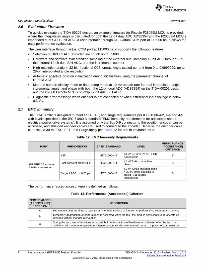
2.7 EMC ImmunityThe TIDA-00202 is designed to meet ESD, EFT, and surge requirements per IEC61000-4-2, 4-4 and 4-5with levels specified in the IEC 61800-3 standard "EMC immunity requirements for adjustable speed,electrical-power drive systems". It is assumed only the SubD-9 connector to the position encoder can beaccessed, and shielded encoder cables are used to connect to the encoder. Because the encoder cablecan exceed 30 m, ESD, EFT, and Surge apply per Table 12 for use in environment 2.
Table 12. EMC Immunity Requirements
PORT PHENOMENON BASIC STANDARD LEVELPERFORMANCE(ACCEPTANCE)
CRITERION
HIPERFACE encoderinterface connecter
ESD IEC61000-4-2 ±4-kV CD or 8-kV AD, if CDnot possible B
Fast transient burst (EFT) IEC61000-4-4 ±2 kV/5 kHz, capacitiveclamp B
Surge 1.2/50 µs, 8/20 µs IEC61000-4-5
±1 kV. Since shielded cable> 20 m, direct coupling toshield (2-Ω sourceimpedance)
B
The performance (acceptance) criterion is defined as follows:
Table 13. Performance (Acceptance) Criterion
PERFORMANCE(ACCEPTANCE)
CRITERIONDESCRIPTION
A The module shall continue to operate as intended. No loss of function or performance even during the test
B Temporary degradation of performance is accepted. After the test, the module shall continue to operate asintended without manual intervention.
C During the test, loss of functions accepted, but no destruction of hardware or software. After the test, themodule shall continue to operate as intended automatically, after manual restart, or power off, or power on.
Sin+
Sin-
Cos+
Cos-
5 V
3.3 V
Sin(analog)
Sin (TTL)
Cos (TTL)
ADS7254
ADC
ADC
24-V input
VREF
HIPERFACE encoder
11 V
12 V
Enc
oder
con
nect
or
SPI(Sin, Cos)
/CS
THS4531A
TLV3202
Option 1:Dual ADC with SPI
Option 2:Dual analog out
GND
VENC
TIDA-00202
Comparatorblock
Cos(analog)
OPA2365
RS-485 transceiver
SN65HVD72
Data+
Data-
Data_tx(TTL)
Data_tx_en (TTL)
Data_rx(TTL)
Hos
t pro
cess
or c
onne
ctor
DC/DCBuck
TPS5401
DC/DCBuck
TPS560200
LDOTPS79933
LDOLP2954
TLV431
www.ti.com Block Diagram
9TIDUB64A–December 2015–Revised March 2016Submit Documentation Feedback
Copyright © 2015–2016, Texas Instruments Incorporated
Interface to a HIPERFACE Position Encoder
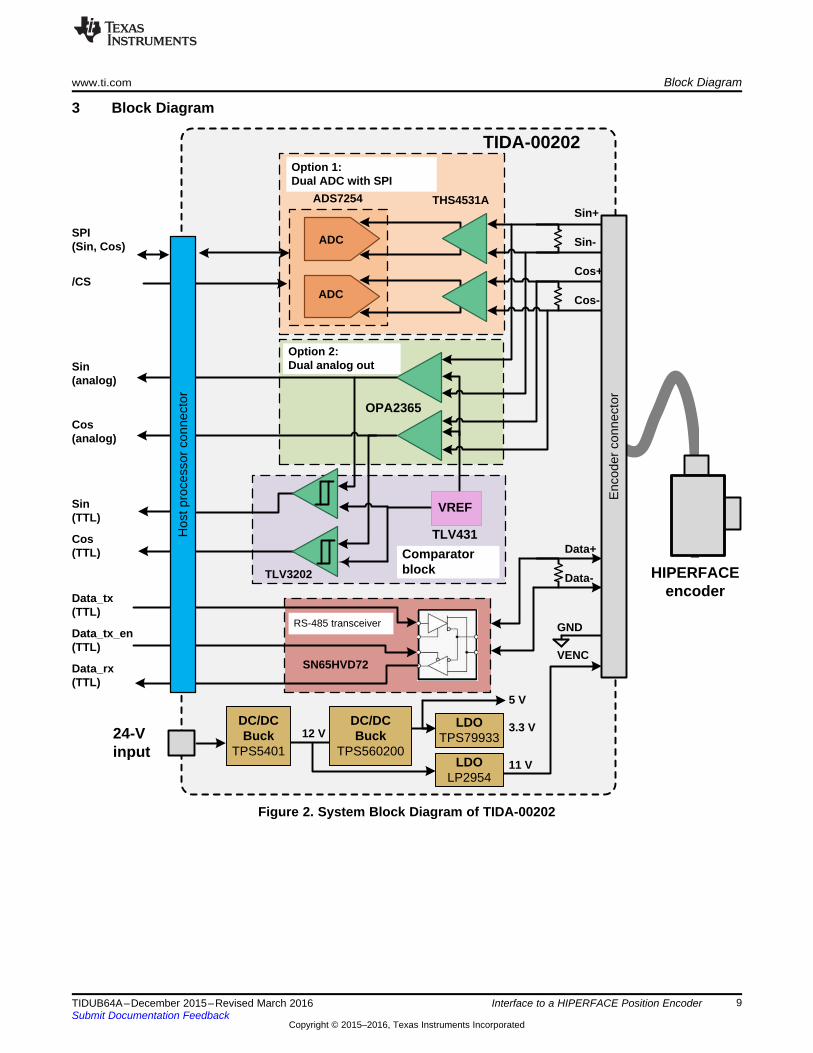
3 Block Diagram
Figure 2. System Block Diagram of TIDA-00202

CDAC
Comparator
SAR
CDACS/H
SAR
Comparator
Serial
Interface
ADC_A
ADC_B
S/H
REF_A
REF_B
Block Diagram www.ti.com
10 TIDUB64A–December 2015–Revised March 2016Submit Documentation Feedback
Copyright © 2015–2016, Texas Instruments Incorporated
Interface to a HIPERFACE Position Encoder
3.1 Highlighted ProductsThe following key products are used in this design with the key features highlighted.
3.1.1 ADS7254The ADS7254 has been selected for the following reasons:• Dual-channel, simultaneous sampling, with true differential inputs and dual or independent reference
voltages to improve immunity against common mode noise• High resolution (12-bit) with high precision (superb THD and SNR performance of –72-dB SNR,
–90-dB THD)• Drop-in pin-compatible 14-bit and 16-bit versions for flexibility pending required resolution versus cost
optimization• High speed (1 MSPS) and bandwidth to support at least 500-kHz analog input signals• Sample point triggered by hardware (falling edge of /CS) allows host processor to precisely
synchronize the sample point with the incremental counter latch.• Dual, programmable, and buffered 2.5-V internal reference to provide common mode bias voltage to
amplifier to almost cancel offset and offset drift-related errors• Serial interface to host processor (dual data) with up to 24-MHz clock frequency to minimize latency• Fully-specified over the extended industrial temperature range: –40°C to 125°C• Small package
Figure 3. ADS7254 Block Diagram

RG
RG RF
RF
VS+
THS4531A
VS±
VOUT+
VOUT±VIN+
VIN±
+
±
Differential
Input
Differential
Output
www.ti.com Block Diagram
11TIDUB64A–December 2015–Revised March 2016Submit Documentation Feedback
Copyright © 2015–2016, Texas Instruments Incorporated
Interface to a HIPERFACE Position Encoder
3.1.2 THS4531ATo leverage the ADS7254 performance, the design requires a fully differential, high-speed amplifier withconfigurable output common mode voltage, like the THS45xx family.
Figure 4. Differential Input to Differential Output Amplifier
The signal remains fully differential. The gain and optional filtering is defined by the input and feedbackresistors and capacitors. The gain is set by the ration of RF/RG and the output common-mode voltage isset by the input signal VOCM.
The THS4531A was chosen as it meets the topology and can drive the ADS7254. A single amplifiertopology per package was used instead of the dual differential amplifier per package like the THS4532 forflexibility and easier PCB routing.
The key parameters of the THS4531A for use in this design are:• Fully-differential architecture with adjustable output common-mode voltage• High gain bandwidth: 27 MHz (6 MHz at G = 5)• Low distortions, THD -120 dBc at 1 kHz (1 VRMS, RL = 2 kΩ)• Low input voltage noise: 10 nV/√Hz (f = 1 kHz)• Very low offset, VOS: ±100 μV• Very low offset drift, VOS Drift: ±2 μV/˚C (industrial temperature range)• Single 5-V supply to leverage same supply than ADS7254• Rail-to-rail output (RRO) and negative rail input (NRI) to maximize input and output signal swing
3.1.3 OPA2365For the input buffer and the differential to single-ended conversion, the OPA2365 has been selected dueto:• 2.2 to 5.5-V operation to leverage 5-V rail• Rail-to-rail I/O• Very low offset and offset drift: 200 µV (max) and 1 µV/K (typically)• Low voltage and current noise: 4.5 nV/√(Hz) and 0.004 pA/√(Hz)• Excellent THD+N: 0.0004%• High common-mode rejection, CMRR: 100 dB (min)• Slew rate: 25 V/μs• Fast settling: 300 ns to 0.01% to drive external ADC
Other options include the OPA2322, which is a lower cost alternative, with 2-mV offset voltage and slightlyreduced AC and DC performance.

Block Diagram www.ti.com
12 TIDUB64A–December 2015–Revised March 2016Submit Documentation Feedback
Copyright © 2015–2016, Texas Instruments Incorporated
Interface to a HIPERFACE Position Encoder
3.1.4 TLV3202The comparators selected are the TLV3202 (dual comparators), 40 ns, microPOWER, and push-pulloutput comparators with the following main characteristics:• Low propagation delay of typical 40 ns• Low input offset voltage of typical 1 mV to ensure minimum drift of switching threshold• Push-pull outputs, to drive the input of a 3.3-V I/O host processor• Industrial temperature range
3.1.5 SN65HVD72The following parameters were considered regarding RS-485 transceivers:• 3.3-V supply• 3.3-V I/O with 5-V tolerant logic inputs• Max 250 kBaud• Large receiver hysteresis (80 mV) for improved noise rejection• IEC61000-4-2 ESD (absolute maximum ratings): ±12 kV (contact discharge)• IEC61000-4-4 EFT (absolute maximum ratings): ±4 kV
3.1.6 TLV431The TLV431 is a low-voltage 3-terminal adjustable voltage reference with specified thermal stability overapplicable industrial and commercial temperature ranges. Output voltage can be set to any value betweenVREF (1.24 V) and 6 V with two external resistors. These devices operate from a lower voltage (1.24 V)than the widely used TL431 and TL1431 shunt-regulator references.• Output voltage between 1.24 and 6 V using resistor divider• Typical temperature drift 6 mV (–40°C to 85°C)• Reference voltage tolerance 1.5%
The TLV431 is pin-to-pin compatible with the TLV431A, which has a better reference voltage toleranceand temperature drift between –40°C to 85°C.
3.1.7 TPS5401The TPS5401 is a 42-V, 0.5-A, step-down regulator with an integrated high-side MOSFET. Current-modecontrol provides simple external compensation and flexible component selection. A low-ripple pulse-skipmode reduces the supply current to 116 μA when outputting regulated voltage with no load. Using theenable pin, the shutdown supply current is reduced to 1.3 μA when the enable pin is low.• High efficiency at light loads with a pulse-skipping Eco-mode™ control scheme• 3.5- to 42-V input voltage range• 0.8-V ±3.5% internal voltage reference (device dependent)
The TPS5401 is pin-to-pin compatible with the following devices:• TPS54040A with similar performance but more accurate output voltage and enable threshold• TPS54140A, TPS54240, TPS54340, and TPS54540 with higher current options if more current are
needed in different designs
www.ti.com Hardware Design
13TIDUB64A–December 2015–Revised March 2016Submit Documentation Feedback
Copyright © 2015–2016, Texas Instruments Incorporated
Interface to a HIPERFACE Position Encoder
4 Hardware DesignThis section describes the different sub-modules of the complete design, explaining the choices madeduring the component and schematic process. The sub-modules explained are:• Analog parameter channel signal chain• Digital parameter channel signal chain• Power supply• Host processor interface
4.1 Analog Parameter Channel Signal ChainFor the analog signal chain, two optional paths are implemented:• A fully differential signal path with digital SPI output, featuring fully differential amplifiers and fully
differential dual 12-bit simultaneous sampling ADC with SPI output• Dual analog differential input to single-ended analog dual outputs, to drive the comparator and connect
to dual ADC for host processors with embedded ADCs
The dual analog path offers the option to either test the design with the onboard 12-bit dual path or usethe analog differential to single-ended path with an MCU and embedded ADC. Additionally, sincedecoupled through a buffer from the high-resolution path, the analog path ensures ideal decoupling of thecomparator path. This avoids crosstalk into the external analog path when switching output level duringsine and cosine zero crossing.
Another use case would use both paths. One path for improved noise immunity with reduced bandwidth tofilter out HF noise, while the other path would have offer standard bandwidth up to maximum speed. Thelower bandwidth with improved noise immunity would be dedicated to the onboard 12-bit ADC, while theother path with standard bandwidth would be connected to the MCU with an embedded ADC.
The comparator subsystem will generate TTL level outputs for signals SIN and COS at a very low-propagation delay.
The following subsections explain each subsystem.

SIN_P1
SIN_M1
SIN_P
SIN_M
220pFC74
220pFC70
V5_dc
GNDD13ZHCS350TA
D14ZHCS350TA
GNDV5_dc
D16ZHCS350TA
D15ZHCS350TA
220pFC78
GND
GND
0
R86
0
R92
130R89
SIN_P1
SIN_M1
GND
47µH
L7
47µH
L8
1.00kR84
1.00kR95
IO11
IO22
GND3
U17
TPD2E007DCKR
DNP
Hardware Design www.ti.com
14 TIDUB64A–December 2015–Revised March 2016Submit Documentation Feedback
Copyright © 2015–2016, Texas Instruments Incorporated
Interface to a HIPERFACE Position Encoder
4.1.1 Option 1: Fully Differential Signal Path With Dual 12-Bit ADC With SPI
4.1.1.1 Input Signal Termination and ProtectionFigure 5 shows the TIDA-00202 schematics of the input stage for the encoder’s differential signals SINand COS.
Figure 5. Termination for the Analog Inputs (SIN Input Shown)
The differential input signals are terminated with 130-Ω resistors each. Optional series 47-µH inductors areused for increased HF immunity along with around 120-kHz bandwidth.
Looking at the encoder signals SIN+/SIN– (named "SIN_P – SIN_M" in the schematic) signal conditioningblock schematic from left to right, the following parts and functions can be distinguished:• The series inductors L7 and L8 with 47 µH per HIPERFACE standard optional recommendation for
high-frequency filtering. These are optional in this design and not recommended when accurate gainand minimum temperature related gain drift is mandatory.
• The HF noise suppression COG capacitors: C35, C38, and C41. For higher common-mode rejection,an additional 2-nF COG capacitor might be placed in parallel to the 220-pF capacitor from eachdifferential input to GND.
• The impedance matching and termination resistor with parallel GND connection 130 Ω, 1k to GND:R89, R95, and R84
• Clamping diodes and op amp input protections (D13 to D16) to the 5-V rail and GND

0.1µF
C59
GND
GND
0.1µF
C71
GND
GND
GND
10µF
C60
10µF
C62
GND
GND
10µFC72
10µFC73
GND
0.22R87
0.22R88
SCLK
SDI
CSn
SDO_A
SDO_B
REFIO_COS
REFIO_COS
REFIO_COS
REFIO_SIN
REFIO_SIN
REFIO_SIN
V5_dc
V5_dc
V5_dc
V3_3_dc
1000pFC64
1000pFC76
10.0
R70
10.0
R77
10.0
R90
10.0
R93
22
R72
22
R781
2
3
4
5
6
7
8
VOCMV+
V-
U16THS4531AIDGK
1
2
3
4
5
6
7
8
VOCMV+
V-
U18THS4531AIDGK
SIN_P1
SIN_M1
COS_P1
COS_M1
0.1µF
C58
0.1µF
C69
2200pFC63
2200pFC75
10
R74
10
R91
0.1µFC66
0.1µFC77
GND
GND
3.0R81
3.0R82
3.0
R71
3.0
R75
1.00kR79
4.99kR80
220pFC67
1.00kR68
4.99kR66
220pFC57
1.00kR94
4.99kR96
220pFC79
1.00kR85
4.99kR83
220pFC68
REFIO_A3
AINP_A1
CS11
DVDD9
SDI10
SCLK12
AINM_A2
REFGND_A4
AINM_B7
SDO_B14
REFIO_B6
SDO_A13
GND15
AVDD16
AINP_B8
REFGND_B5
U15
ADS7254IPWR
www.ti.com Hardware Design
15TIDUB64A–December 2015–Revised March 2016Submit Documentation Feedback
Copyright © 2015–2016, Texas Instruments Incorporated
Interface to a HIPERFACE Position Encoder
4.1.1.2 Differential Amplifier THS4531A and 12-Bit ADC ADS7254The two primary circuits, required to maximize the performance of a high-precision, successiveapproximation register (SAR) ADCs, are the input driver and the reference driver circuits. For details onselecting the amplifier, refer to Section 9.1 of the ADS7254 datasheet (SBAS556).
The THS4531A has been minded to work in combination with the ADS7254. The common-mode / DC-level of the input signal (2.5 V nominal) is provided to the THS4531A directly from the reference output ofthe ADS7254 itself to minimize potential offset and drift errors.
The differential input full-scale range (FSR) of the ADS7254 was configured to ±2 × VREF. With thereference voltage of VREF = 2.5 V, this yields a FSR of ±5 V. The maximum HIPERFACE encoder’sdifferential input voltage is 1.1 VPP. A voltage of higher than 1.35 VPP should still be detected as a failure. Asafety margin of 50% is added to the maximum peak-to-peak voltage, which is 1.8 VPP. To match the ADCfull-scale input range, the gain of the THS4531A should be 5.5. However, to remain in the linear outputvoltage range of the THS4531A at a 5-V supply, which is at least 0.25 to 4.8 V, the gain should bereduced by around 10%, hence the ideal differential amplifier gain would be 5.
To ensure a minimum gain error and especially drift between the channels, resistors with 0.1% accuracyand low temperature drift are needed. To minimize noise, the feedback resistors should be chosen in thelower kΩ range.
Due to the gain of 5, a typical 1-VPP input signal leverages around 50% of the ADC FSR, which results in aloss of 1-bit of precision, hence yielding equivalent 11-bit resolution.
Figure 6 shows the schematics of the ADC with SPI signal path, the gain setting resistors are R66, R68,R79, R80, R83, R85, R94, and R96.
The parallel 220-pF feedback capacitors C57, C67, C68, and C79 were chosen for a 150-kHz (–3-dB)bandwidth.
Figure 6. SIN and COS Signal Chain With Dual THS4531A and ADS7254
NOTE: The SIN input is connected to the ADS7254 channel B and the COS input to channel A foroptimum performance layout and minimum numbers of vias.

Hardware Design www.ti.com
16 TIDUB64A–December 2015–Revised March 2016Submit Documentation Feedback
Copyright © 2015–2016, Texas Instruments Incorporated
Interface to a HIPERFACE Position Encoder
The series 10-Ω resistors R70, R77 and the 2.2-nF and 1-nF capacitors C63, C64 (R90, R96, C75, andC76 for ADS7254 channel B) from the anti-aliasing filter. The filter capacitor C63 and C64 (C75 and C76),connected across the ADC inputs, filters the noise from the front-end drive circuitry, reduces the samplingcharge injection and provides a charge bucket to quickly charge the internal sample-and-hold capacitorsduring the acquisition process. As a rule of thumb, the value of this capacitor should be at least 10 timesthe specified value of the ADC sampling capacitance. For these devices, the input sampling capacitanceis equal to 40 pF. The capacitor should be a COG- or NPO-type because these capacitor types have ahigh-Q, low-temperature coefficient, and stable electrical characteristics under varying voltages,frequency, and time. To avoid amplifier stability issues, 10-Ω series isolation resistors R70, R77 (R90,R96) are used at the output of the amplifiers. For details, refer to the section 9.1 of the ADS7254datasheet (SBAS556).
To minimize the impact of an offset drift of the ADC reference REFIO_SIN and REFIO_COS, the ADCreferences are used to bias the common-mode output voltage of the THS4531A. To buffer and decouplethe VOCM signal at the THS4531A, small RC filters R74/C66 and R91/C77 R87, R88, C72, and C73 areadded close to each pin.
The ADS7254 reference voltages REFIO_A and REFIO_B are decoupled with a 10-µF capacitor C72 andC73, respectively, and a 0.22-Ω resistor is added in series to avoid high-frequency oscillations.
To optimize the layout for cross-talk with minimum use of vias for the critical signals SIN+, SIN– andCOS+, COS–, the following connections have been made:1. The differential input signal SIN (SIN+, SIN–) has been inverted at the input of the THS4531A and
again inverted by connecting to the ADS7254 input channel AINM_B and AINM_P.2. The differential output signal of the THS4531A, COS+ and COS–, have been connected to the
ADS7254 input pins AINP_A to COS– and AINM_A to COS+.
This results in the following hardware relationship. The ADS7254 channel B equals the HIPERFACEencoder signal SIN. The ADS7254 channel A equals the HIPERFACE encoder signal COS.
The configuration of the ADS7254 registers through serial interface is explained in Section 4.3.

GND
GND
V5_dc
GND
GND
220
R36
8.45k
R46
8.45k
R34
GND
4.75k
R44
GND
4.75k
R38
GND
220
R45
GND
1
2
3
48
U10AOPA2365AIDR
5
6
7
48
U10BOPA2365AIDR
100pFC38
100pFC40
120pF
C43
120pF
C31
0.1µFC32
GND
V5_dc
0.1µFC35
GND
332
R37
332
R43
V5_dc
REFIO
1
2
3
48
U11AOPA2365AIDR
47pFC37
47pFC41
D7ZHCS350TA
V3_3_dc
0.01µFC42
2200pFC33
10.0
R39
20.0
R32
GND
SIN_P1
SIN_M1
www.ti.com Hardware Design
17TIDUB64A–December 2015–Revised March 2016Submit Documentation Feedback
Copyright © 2015–2016, Texas Instruments Incorporated
Interface to a HIPERFACE Position Encoder
4.1.2 Option 2: Analog Signal Path With Single-Ended Output for MCU With Embedded ADCThe parallel analog signal path should not impact the high-resolution path and especially the differentialamplifier. Therefore, the differential signals SIN+,SIN– and COS+,COS– are tapped off after the inputtermination and protection and are buffered using unity gain amplifiers with very low offset and especiallyoffset drift. The following amplifier should convert the differential signals into a single-ended signal. Theminimum bandwidth should be least 150 kHz. The phase delay for the path to the comparator should besimilar than the high-resolution path to ensure minimum phase lag.
The supply voltage should be a single supply of 5 V to support input common-mode voltages up to 3.5 V.
To match the high-resolution channel, the sum of the offset drift of both op amps should be at least 12-bitequivalent accuracy.
The analog output voltage should be scaled from 0 to 3.3 V with a 1.65-V common mode. Applying thesame criteria in Section 4.1.1 with a maximum 1.1-VPP input voltage and a 20% margin with regards to the3.3-V FSR, the max gain yields 1.67.
Figure 7 shows the analog signal chain for channel SIN. The channel COS is identical.
Figure 7. Analog Signal Path With Differential Input to Single-Ended Output for Signal SIN(Signal COS Not Shown)
The differential signals SIN_P and SIN_N are connected through a 220-Ω resistor to the non-invertinginput of the OPA2365 (U10A and U10B). The OPA2365 (U10A and U10B) are configured as unity-gainbuffer to avoid loading the source and introducing distortions. The 220-Ω series resistor limits the currentinto the non-inverting input of the OPA2365 in case of an over- or undervoltage event. The output of eachbuffer employs a small, adjustable RC-filter with, for example, R37 and C38 in Figure 7 with f–3dB ~ 5 MHzfor high-frequency noise reduction.
The following OPA2365 (U11A) is configured as differential to single-ended amplifier and level shifter. Thegain is set to 1.67 and the output common-mode voltage to 1.65 V through a low-voltage adjustableprecision shunt regulator TLV431. An adjustable 120-pF feedback capacitor is added in parallel to the8450-Ω feedback resistor to low-pass filtering with a 150-kHz (–3-dB) bandwidth, ideally matched to theTHS4531A bandwidth.
The 1.65-V bias voltage is decoupled with a 10-nF capacitor (C42) each.
Because the OPA2365 is supplied with 5 V, the output of the amplifier is clamped to 3.3 V (D7) with aseries 10-Ω current limiting resistor (R39). This is to protect the following comparator (TLV3202) and anexternal ADC, which typically are 3.3-V FSR.
An anti-aliasing and decoupling RC network (R32/C33) is added to drive an external ADC. The filter wasoptimized for use with the embedded 12-bit dual S/H ADC in the C2000 Piccolo MCU family. For otherADCs, the filter has to be adjusted accordingly.

Hystereis
R41V 3.3 V ~ 160 mV
R42= ´
( ) GHystereis Out_High Out_Low
F
RV V V
R= - ´
SIN_A
GND
GND
SIN_TTL
GND
0.1µFC34
GND
V3_3_dc
GND
0.01µFC36
1.0
R33
REFIO
10.0
R35
2
3
1A
V+
V-
84
U12ATLV3202AID
V_dc1
D7ZHCS350TA
V3_3_dc2200pFC33
2200pFC39
10.0
R39
26.7k
R41
20.0
R32
20.0
R40
549k
R42
Hardware Design www.ti.com
18 TIDUB64A–December 2015–Revised March 2016Submit Documentation Feedback
Copyright © 2015–2016, Texas Instruments Incorporated
Interface to a HIPERFACE Position Encoder
4.1.3 Comparator Subsystem for Digital Signals SIN and COSThe comparators are used to detect the zero-crossing of the analog signals SIN and COS and generatethe corresponding digital 3.3-V TTL-compatible signals SINTTL and COSTTL.
The TLC372 dual comparator with a 250-ns propagation delay is a lower cost option, depending overallsystem propagation delay and maximum frequency. It is normally sufficient for signals up to 150-kHzmaximum frequency, as with the HIPERFACE encoder used in this design. However, the advantage of theTLV320x family is that it allows other components or the hysteresis to add more delay while still keepingthe phase lag below 90 degrees (for example, 500 ns at a 500-kHz signal frequency). For example, alarger hysteresis would increase the propagation delay while improve immunity against noise.
4.1.3.1 Non-Inverting Comparator With Hysteresis DesignThe input signals to all comparators are derived from the output of the single-ended to differentialamplifier. The output signal is clamped to 3.3 V, as described in Section 4.1.2, and decoupled with an RCnetwork (like R40 and C39 in Figure 8 for the SIN signal) to avoid crosstalk to the analog single-endedsignals SIN and COS, respectively.
To match the phase between the high-resolution path and this path, the RC decoupling network at theinput to the comparator matches the RC filter (2 × 10 Ω and 2.2 nF) at the THS4531A output.
The TLV3702 is configured as a non-inverting comparator to detect the zero-crossing of the analog sineand cosine signals, SIN and COS. Figure 8 shows the corresponding schematics for the signal SIN.
Figure 8. Comparator With Hysteresis for SIN Signal
The switching threshold is set by the reference voltage VREF = 1.65 V (TLV431), which is also used to biasthe single-ended analog signals for the differential to single-ended amplifiers. For each comparator, thereference input is taken from the TLV431and decoupled with a 10-Ω series resistor and a 10-nF capacitor.
A hysteresis is added for better noise immunity. The hysteresis (VTH+ – VTH–) of a non-inverting comparatorcan be calculated per Equation 1:
(1)
with VOut_High the high-level and VOut_Low the low level comparator output voltage, RF the feedback and RGthe input resistor into the non-inverting comparator input.
For the configuration of this design as outlined in Figure 8, the hysteresis has been set to around 160 mVper Equation 1. Since R39 and R40 are magnitudes lower than R41, they can be neglected.
(2)

1Hysteresis
IN_PEAK PEAK
160 mV~ sin
V
-
-
æ öf ±ç ÷
ç ÷è ø
( )TH
R41V 3.3 V 1.65 V 1 1.57 V
R42-
æ ö= - ´ - =ç ÷
è ø
TH
R41V 1.65 V 1 1.73 V
R42+
æ ö= ´ + =ç ÷
è ø
www.ti.com Hardware Design
19TIDUB64A–December 2015–Revised March 2016Submit Documentation Feedback
Copyright © 2015–2016, Texas Instruments Incorporated
Interface to a HIPERFACE Position Encoder
The upper and lower switching thresholds VTH+ and VTH– are defined per Equation 3 and Equation 4 withthe reference voltage VREF = 1.65 V.
(3)
(4)
CAUTIONThe lower threshold is a function of the supply voltage. However, the supplyvoltage tolerance of this design 5%, as typical with most designs. A ±5%tolerance with the 3.3-V supply voltage would affect the lower threshold by onlyby ±16 mV, resulting VTH– range from approximately 1.56 to 1.59 V, hence stillacceptable.
The 3.3-V supply of each comparator is decoupled with a 1-Ω series resistors and a 100-nF capacitor tominimize crosstalk through the 3.3-V rail to other comparators.
The hysteresis allows for a clean digital signal, meaning it avoids fast switching due to noise around thezero crossing point. The hysteresis, however, introduces an additional propagation delay, which dependson the analog signal amplitude VIN_PEAK-PEAK at the comparator input.
(5)
Assuming a minimum input voltage of 0.9 VPP, the output of the differential- to single-ended amplifier(gain = 1.67) will have an amplitude of 1.5 VPP (0 to 10 kHz) and around 0.9 VPP at 150 kHz due to low-pass filter attenuation. The hysteresis corresponding phase delay of the digital signals SIN and COS willbe around 10 degrees for a 0.9-VPP input at the comparator. At 150 kHz, this would translate into a totalpropagation delay of the comparator of around 190 ns + 40 ns =230 ns.
Due to the low propagation delay of the TLV3201 with only 40 ns, the overall delay of the comparatorblock remains well below 30 degrees up to 150 kHz and offers a sufficient margin for an additional phaselag due to tolerances and sample instant synchronization by the embedded processor.
The comparator for the COS signal has the same settings.
4.1.3.2 Comparator Subsystem Connected to THS4531A OutputFor this design, the comparator subsystem was leveraging the differential-to-single-ended signal path forbuffering and signal conditioning. For example, to connect the comparator subsystem to the differentialsignal path at the output of the THS4531A, refer to the TI Design TIDA-00178.

0.1µFC28
GND
GND
GND
22
R25
GND
10kR29
1.00kR31
1.00kR24
130R27
V3_3_dc
Data_RX
Data_TX_EN
RS485_M
RS485_P
GND
GND
330pFC29
330pFC30
V3_3_dc
10
R26
10
R28
VCC8
RE2
D4
DE3
GND5
A6
B7
R1
U7
SN65HVD72DR
GNDData_TX
10kR30
V3_3_dc
IO11
IO22
GND3
U8
TPD2E007DCKR
Hardware Design www.ti.com
20 TIDUB64A–December 2015–Revised March 2016Submit Documentation Feedback
Copyright © 2015–2016, Texas Instruments Incorporated
Interface to a HIPERFACE Position Encoder
4.2 Digital Parameter Channel Signal ChainWhen choosing the RS-485 for HIPERFACE, it is important to remember that the protocol is based on aUART protocol with a maximum baud rate of 38.4 kBaud and that HIPERFACE does not compensate forpropagation delay. When HIPERFACE is implemented at maximum clock compared to cable length, theentire loop propagation delay (master and encoder) must not exceed 13 μs.
With this information, the SN65HVD72 was the chosen RS-485 device.
4.2.1 RS-485 Termination and Transient ProtectionFigure 9 shows the RS-485 transceiver schematics for the digital parameter channel.
Figure 9. RS-485 Transceiver Configuration for HIPERFACE DATA+/DATA–
A single 130-Ω/0.4-W resistor was chosen as line termination resistor according to HIPERFACEspecification.
A 10-Ω pulse-proof resistor is added into the SIN and COS bus lines if a transient voltage is higher thanthe specified maximum voltage of the transceiver bus terminals (see R26 and R28 in Figure 9). Theseresistors limit the residual clamping current into the transceiver and prevent it from latching up. In datareceive mode, due to the low input current of the typical 240 µA, the voltage drop across the 10-Ωresistors is negligible. In data transmit mode, the voltage drop across both 10-Ω resistors is around 15%,which results in a slightly lower transmit differential voltage.
To further improve immunity against common-mode noise a 330-pF bypass capacitor is added from eachdifferential RS-485 output DATA+ and DATA– to GND (see C29 and C30 in Figure 9).
The bus terminals of the SN65HVD7x transceiver family possess on-chip ESD protection against ±15-kVhuman body model (HBM) and ±12-kV IEC61000-4-2 contact discharge.
Because ESD and EFT transients have a wide frequency bandwidth from approximately 3 MHz to 3 GHz,high-frequency layout techniques must be applied during PCB design. A complete list of layout guidelinescan be found in the SN65HVD72 datasheet (SLLSE11). This design has especially implemented:• VCC and ground planes to provide low-inductance• 100-nF bypass capacitors as close as possible to the VCC pins of the transceivers and other digital
logic• At least two vias for VCC and ground connections of bypass capacitors and protection devices to
minimize effective via inductance.

D1
MBRA160T3G
GND
10
R1
2.2µFC9
2.2µFC10
0.01µFC6
1µFC5
6.8µH
L1
0.1µFC7
0.1µFC8
DC/DC BuckTPS5401
12 V 400 mAInput
filter24-V DC
(17 to 36 V)
LDOTPS79933
3.3 V 100 mA
LDOLP2954
11 V 250 mA
5 V 400 mADC/DC Buck
TPS560200
www.ti.com Hardware Design
21TIDUB64A–December 2015–Revised March 2016Submit Documentation Feedback
Copyright © 2015–2016, Texas Instruments Incorporated
Interface to a HIPERFACE Position Encoder
4.3 Power ManagementPower management consists a DC/DC buck to generate a 12-V intermediate rail from the 24-V inputvoltage and a second DC/DC buck to generate the 5-V rail. The encoder supply voltage is derived fromthe intermediate 12-V rail. The 3.3-V rail is derived from the 5-V rail, as shown in Figure 10.
Figure 10. Power Management Subsystem
Because of the high performance required by the system and solution, most of the power rails areprovided by low-noise LDOs. The drawback is the limited efficiency and low-output current capability. Themaximum output current is limited by the thermal performance due to the high power losses.
A typical system would include the host processor for the HIPERFACE master (like a C2000 PiccoloMCU) on the same PCB. Therefore, the TIDA-00202 5-V intermediate rail was chosen to support at least400 mA to provide sufficient current for the processor as well.
Minimize the noise introduced by both switcher solutions by proper layout and component selection.
4.3.1 24-V Input to 12-V Intermediate RailA switching DC-DC converter is provided to achieve the intermediate voltage rail of 12 V that supplies theencoder supply and the second buck converter. This is basically mandatory because the high VIN / VOUTratio makes any LDO unsuitable for the power conversion.
The selected values for the input filter are shown in Figure 11. For more details about how to design aninput EMI filter, see the application report AN-2162 Simple Success With Conducted EMI From DC-DCConverters (SNVA489).
Figure 11. Input Filter Including Reverse Polarity Protection
The DC/DC buck converter has been designed to meet the following specifications:• Input voltage: VIN = 17 to 36 V, 24 V nominal• Output voltage: 12 V at 500 mA• Switching frequency: 500 kHz nominal• Output voltage ripple: 25 mVPP max• Efficiency: > 80% at full load• Non-isolated topology

12 V 0.8 VR6 10 k 140 k
0.8 V
æ ö-= W ´ = Wç ÷
è ø
2.2µFC9
2.2µFC10
D2MBRA160T3G
GND
GND
GNDGND
Green
21
D3
0.1µF
C1
100µH
L2
744065101
10µFC2
10µFC3
10µFC4DNP
4700pFC13
16pFC12
681kR2
2200pFC11
10.0kR8
46.4kR5
80.6kR4
140kR6
237kR7
GND
8.66kR3
BOOT1
VIN2
EN3
SS/TR4
RT/CLK5
PWRGD6
VSENSE7
COMP8
GND9
PH10
TP11
U1
TPS5401DGQR
Hardware Design www.ti.com
22 TIDUB64A–December 2015–Revised March 2016Submit Documentation Feedback
Copyright © 2015–2016, Texas Instruments Incorporated
Interface to a HIPERFACE Position Encoder
The TPS5401 is selected because it is a buck converter with an integrated FET, a 3.5- to 42-V inputvoltage, and a 0.8- to 39-V output voltage at a 500-mA output current. Its frequency can be adjusted from100 kHz to 2.5 MHz or can be synchronized with an external clock. It can also be enabled and disabled.The features of the TPS5401 fit these specifications well.
Note that the TPS5401 is pin-to-pin compatible with the TPS54040A, which is a higher cost version of theTPS54040A with similar performance but more accurate output voltage and enable threshold.
Also note that the TPS5401 is pin-to-pin compatible also with the TPS54140A, TPS54240, TPS54340, andTPS54540. This widens the part selection and offers flexibility to optimize the design with regards topower versus system cost.
Figure 12. Schematic of 24-V to 12-V DC-DC Buck Converter With TPS5401
For a detailed explanation of the design process, see the TPS5401 datasheet (SLVSAB0) or theTIDA-00180 design guide (TIDU533), which shows the calculation for the TPS54040A.
The output voltage is set through R6 and R8 according to Equation 6:
(6)
The tolerance of the output voltage is better than 5%. This assumes feedback resistors with a 1%tolerance and the internal bandgap tolerance from the TPS5401 of ±3.5%.
The switching frequency is set with R7 = 237 kΩ to 500 kHz.
ENC_Vcc
Green2
1D6
IN8
OUT1
GND4
SNS2
ERR5
SD3
5V TAP6
FB7
U5
LP2954AIM
V12_dc
1µFC24
GND
GND
0.1µFC25806k
R20
100kR22
4.7µFC26
4.7µFC27
LDO_FB
LDO_FB
PWR_EN
V3_3_dc
100kR23
0
R17DNP
0
R19
8.66kR21
11 V 1.23 VR20 R22 140 k
1.23
-æ ö= ´ = Wç ÷
è ø
www.ti.com Hardware Design
23TIDUB64A–December 2015–Revised March 2016Submit Documentation Feedback
Copyright © 2015–2016, Texas Instruments Incorporated
Interface to a HIPERFACE Position Encoder
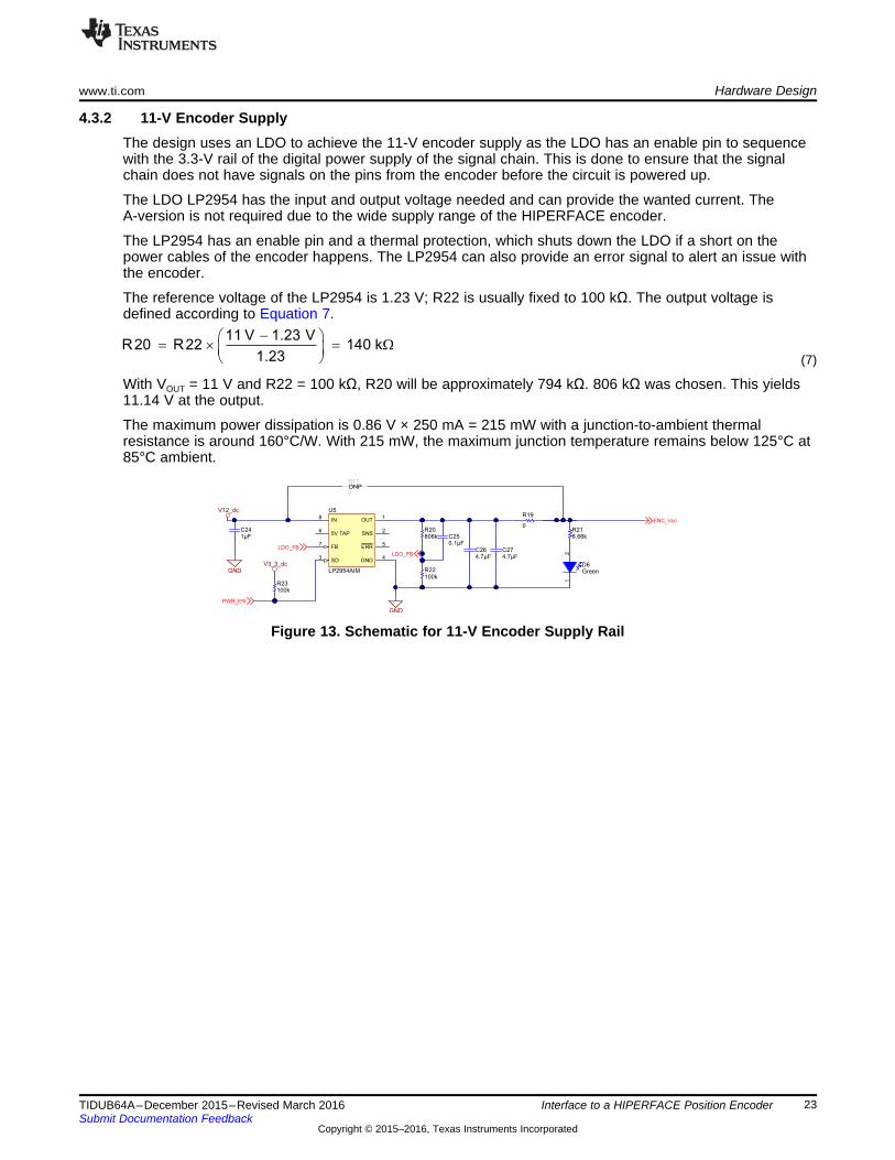
4.3.2 11-V Encoder SupplyThe design uses an LDO to achieve the 11-V encoder supply as the LDO has an enable pin to sequencewith the 3.3-V rail of the digital power supply of the signal chain. This is done to ensure that the signalchain does not have signals on the pins from the encoder before the circuit is powered up.
The LDO LP2954 has the input and output voltage needed and can provide the wanted current. TheA-version is not required due to the wide supply range of the HIPERFACE encoder.
The LP2954 has an enable pin and a thermal protection, which shuts down the LDO if a short on thepower cables of the encoder happens. The LP2954 can also provide an error signal to alert an issue withthe encoder.
The reference voltage of the LP2954 is 1.23 V; R22 is usually fixed to 100 kΩ. The output voltage isdefined according to Equation 7.
(7)
With VOUT = 11 V and R22 = 100 kΩ, R20 will be approximately 794 kΩ. 806 kΩ was chosen. This yields11.14 V at the output.
The maximum power dissipation is 0.86 V × 250 mA = 215 mW with a junction-to-ambient thermalresistance is around 160°C/W. With 215 mW, the maximum junction temperature remains below 125°C at85°C ambient.
Figure 13. Schematic for 11-V Encoder Supply Rail

OUTV 0.8 VR11 R14
0.8 V
-
= ´
EN1
GND2
PH3
VIN4
VSENSE5
U2
TPS560200DBVR
V12_dc
GND
20.0k
R14
V5_dc1
GND
105kR11
GND
0.1µFC14
10µFC16
680pFC18
10µFC15
60 ohm
L4
33µH
L3
7447714330
10µFC17
TP2
Hardware Design www.ti.com
24 TIDUB64A–December 2015–Revised March 2016Submit Documentation Feedback
Copyright © 2015–2016, Texas Instruments Incorporated
Interface to a HIPERFACE Position Encoder
4.3.3 12-V Input to 5-V Intermediate Rail and Point-of-Load SupplyFor the design, a 5-V and a 3.3-V rail is needed, as these rails supply a high-precision analog signalchain. A very low noise rail is needed. Here, an LDO would be ideal. Due to the same powerconsiderations as the 11-V encoder supply, a 12-V to 5-V intermediate rail was done using theTPS560200.
Figure 14. Schematic for 5-V Intermediate Rail
Calculate the output voltage with Equation 8.
The reference voltage of the TPS560200 is 0.8V, R14 is usually fixed to 20 kΩ.
(8)
With VOUT = 6 V and R14 = 20 kΩ, R11 will be approximately 105 kΩ.
From the TPS560200 datasheet (SLVSC81), Equations 4 to 6 were used to calculate the peak and RMScurrent to decide which inductor and output capacitor to use.
Using these equations, a 33-µH inductor was chosen to ensure a low output voltage ripple. With the 33-µHinductor, the output capacitor was chosen to be around 6 µF to have the correct output filter for theTPS560200.
V5_dc
GND
IN1
2
EN3
FB4
OUT5
U3
TPS71701DCKR
DNP
V5_dc1
1µFC20
2.2µFC22
1µFC19DNP
2.2µFC21
0.01µFC23
V3_3_dc
GND
GND
160kR15
DNP
845kR12
DNP
0
R10DNP
0
R16IN
1
2
EN3
NR4
OUT5
GND
U4
TPS79933DDCR
0
R9
Green
21
D4
GND
3.0kR13
Green2
1D5
GND
1.5kR18
www.ti.com Hardware Design
25TIDUB64A–December 2015–Revised March 2016Submit Documentation Feedback
Copyright © 2015–2016, Texas Instruments Incorporated
Interface to a HIPERFACE Position Encoder
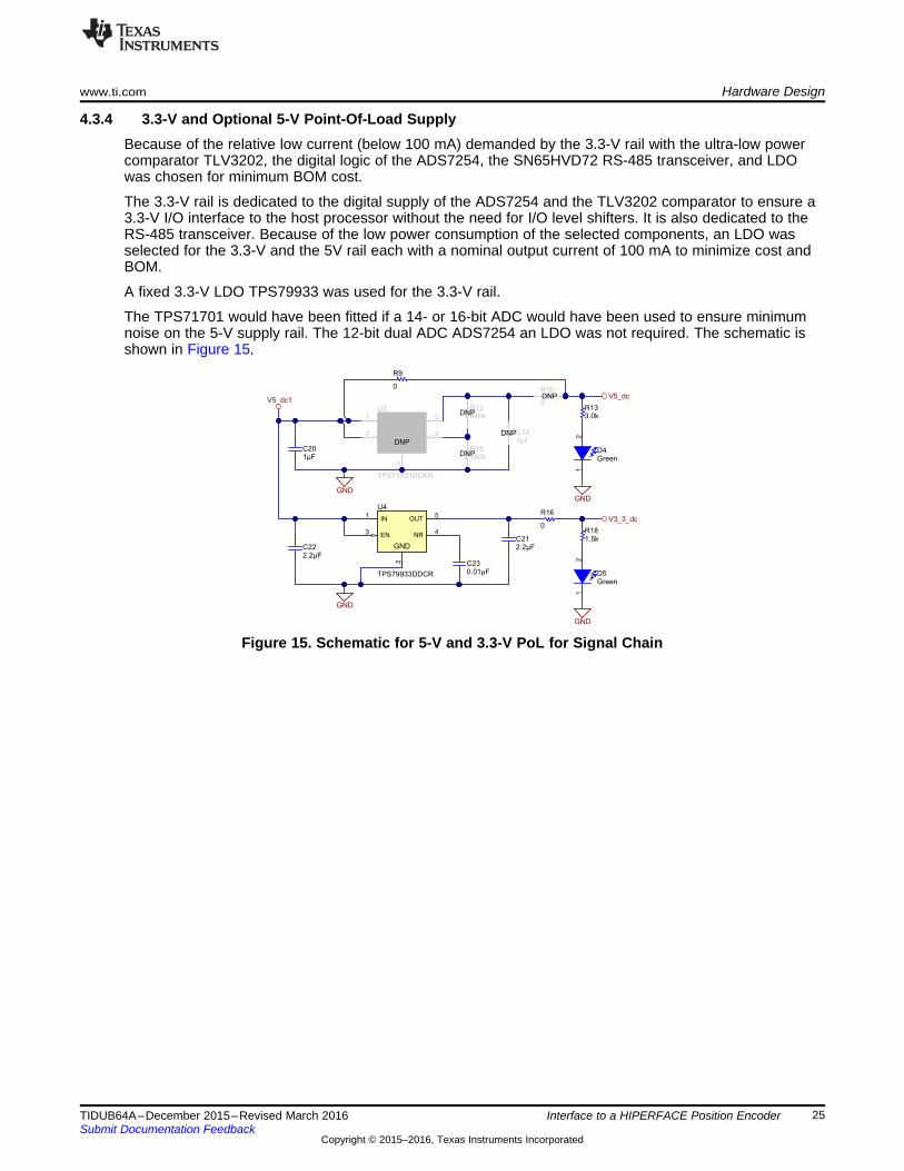
4.3.4 3.3-V and Optional 5-V Point-Of-Load SupplyBecause of the relative low current (below 100 mA) demanded by the 3.3-V rail with the ultra-low powercomparator TLV3202, the digital logic of the ADS7254, the SN65HVD72 RS-485 transceiver, and LDOwas chosen for minimum BOM cost.
The 3.3-V rail is dedicated to the digital supply of the ADS7254 and the TLV3202 comparator to ensure a3.3-V I/O interface to the host processor without the need for I/O level shifters. It is also dedicated to theRS-485 transceiver. Because of the low power consumption of the selected components, an LDO wasselected for the 3.3-V and the 5V rail each with a nominal output current of 100 mA to minimize cost andBOM.
A fixed 3.3-V LDO TPS79933 was used for the 3.3-V rail.
The TPS71701 would have been fitted if a 14- or 16-bit ADC would have been used to ensure minimumnoise on the 5-V supply rail. The 12-bit dual ADC ADS7254 an LDO was not required. The schematic isshown in Figure 15.
Figure 15. Schematic for 5-V and 3.3-V PoL for Signal Chain

Hardware Design www.ti.com
26 TIDUB64A–December 2015–Revised March 2016Submit Documentation Feedback
Copyright © 2015–2016, Texas Instruments Incorporated
Interface to a HIPERFACE Position Encoder
4.4 Host Processor Interface
4.4.1 Signal DescriptionA 20-pin header and a 10-pin header interface are available to connect to a host processor. The headersprovide the necessary signals to calculate the high-resolution interpolated angle for both signal paths,using the ADS7254 dual 12-bit ADC with SPI and an embedded dual S/H ADC on the host processor, ifavailable.
The interface is compliant to 3.3-V I/O systems. To have a solid GND connection, all odd pins areassigned to GND. The signals on the even pins are listed in Table 14.
Table 14. TIDA-00202 Interface Connector to Host MCU
FUNCTION SIGNALS I/O (3.3 V) COMMENT
12-bit high-resolution outputchannel for SIN, COS withADS7254 and SPI (slave)
SDI (I) Digital input Data input for serial communication. Used forconfiguration of dual sampling mode
/CS (I) Digital input
Chip-select signal; active low. Falling edge of /CSlatches the analog input (Hold) and initiates a newconversion. Use falling edge of /CS to latch QEPcounter on host processor synchronously, like onPiccolo MCU
SCLK (I) Digital input, up to 24 MHz Clock for serial communication
SDO_A (O) Digital output
Data output for serial communication, channel Aand channel B. 16-bit 2’s complementary data oneach channel A and channel B. Input to outputsignal gain = 5.
SDO_B (O) Digital output Data output for serial communication channel B
Digital quadrature encodedsignals SIN and COS
SINTTL (O) Digital output 160 mV (±80 mV) hysteresis for SIN and COS,configurable
COSTTL (O) Digital output
Analog single-ended outputchannel for SIN and COS
SIN (O) Analog output: 0 to 3.3 V,1.65-V bias (single-ended)
Nominal output range: 0.82 to 2.48 V(1.65 ±0.83 V) for 1 VPP, gain = 1.67,bias voltage = 1.65 V
COS (O) Analog output: 0 to 3.3 V,1.65-V bias (single-ended)
Nominal output range: 0.82 to 2.48 V(1.65 ±0.83 V) for 1 VPP, gain = 1.67,bias voltage = 1.65 V
Digital RS-485 signals
Data_RX (O) Digital output RS-485 data receive for the UART protocol
Data_TX_EN (I) Digital output RS-485 data transmit enable for the UARTprotocol
Data_TX (I) Digital input RS-485 data transmit for the UART protocol
For details on the connector pin assignment, see Section 6.
CAUTIONIn order to synchronize the analog input sample of the ADS7254 12-bit dualsampling ADC with a QEP incremental counter module, use the /CS signal tothe ADS7254 to latch the QEP counter too. For the MCU, like Piccolo, connectthe /CS to the eQEP Strobe input pin EPEPxS, where x is the module number.The Piccolo eQEPx module can be configured to latch the QEP counter on afalling edge of the EQEPxS pin.

www.ti.com Hardware Design
27TIDUB64A–December 2015–Revised March 2016Submit Documentation Feedback
Copyright © 2015–2016, Texas Instruments Incorporated
Interface to a HIPERFACE Position Encoder
4.4.2 12-Bit Dual ADC ADS7254 With SPI Serial OutputThis section outlines the configuration of the ADS7254 through the serial interface. This is split intoprogramming the full-scale input voltage range with the internal ADS7254 reference and the serial datatransfer.
4.4.2.1 ADS7254 Input Full Scale Range Output Data FormatIn this design, the ADS7254 is intended to be configured for ±2 × VREF input range. The internal referencevoltage VREF should be set to 2.5 V to yield a ±5-V FSR.
Table 15. ADS7254 Transfer Characteristics for TIDA-00202
INPUT VOLTAGEAINP_x - AINM_x MODE INPUT VOLTAGE OUTPUT CODE (HEX)
< –5 V
±2 × VREF RANGE
NFSC 800–5 V + 1 LSB FSR 801
–1 LSB –1 LSB FFF0 0 0
5 V – 1 LSB PFSR – 1 LSB 7FF
The output date format for each channel A and B is 16-bit signed integer output (2’s complementary).
4.4.2.2 ADS7254 Serial InterfaceThe ADS7254 uses the serial clock (SCLK) for synchronizing data transfers in and out of the device. TheCS signal defines one conversion and serial transfer frame. A frame starts with a CS falling edge andends with a CS rising edge. Between the start and end of the frame, a minimum of N SCLK falling edgesmust be provided to validate the read or write operation. As shown in Table 16, N depends upon theinterface mode used to read the conversion result. When N SCLK falling edges are provided, the writeoperation attempted in the frame is validated and the internal user-programmable registers are updated onthe subsequent CS rising edge. This CS rising edge also ends the frame. If CS is brought high beforeproviding N SCLK falling edges, the write operation attempted in the frame is not valid.
Table 16. ADS7254 SCLK Falling Edges for a Valid Write Operation
INTERFACE MODE MINIMUM SCLK FALLING EDGES REQUIRED TO VALIDATE WRITE OPERATION N32-CLK, dual-SDO mode (default) 3232-CLK, single-SDO mode 4816-CLK, dual-SDO mode 1616-CLK, single SDO mode 32
The example firmware on the F28069M Piccolo MCU initializes the ADS7254 in the 32-CLK, single SDOmode.
For more details on the serial interface mode and read and write operations, refer to the AD7254datasheet (SBAS556).

1 2 14 15 16 17 28 29 30SCLK
CS
ADS8353, ADS8354
SDO_A
Sample
N
Sample
N+1
tACQtCONV
tTHROUGHPUT
Data From Sample N
31 32
D1
5-A
18
Data From Sample N
B15 B14 B3SDI
33 34 44 45 46 47 48
ADS7853, ADS7854
SDO_A
Data From Sample N
ADS7253, ADS7254
SDO_A
D1
4-A
D4-
A
D3-
A
D2-
A
D1-
A
D0-
A
D1
5-B
D0-
B
D1-
B
D2-
B
D3-
B
D4-
B
D1
3-A
D1
2-A
D2-
A
D1-
A
D0-
A0 0
D1
3-B00
D0-
B
D1-
B
D2-
B
D1
1-A
D1
0-A
D0-
A0 0 0 0
D1
1-B0000
D0-
B
B2 B1 B0 X X X X X X X X X X X X X
All Devices
SDO_B
Hardware Design www.ti.com
28 TIDUB64A–December 2015–Revised March 2016Submit Documentation Feedback
Copyright © 2015–2016, Texas Instruments Incorporated
Interface to a HIPERFACE Position Encoder
4.4.2.3 ADS7254 Conversion Data ReadAs outlined in Table 16, the device provides four different interface modes to the user. These modes areable to read the conversion result as well. These modes offer flexible hardware connections and firmwareprogramming. In the 32-CLK interface modes, the device uses an internal clock to convert the sampledanalog signal. The conversion is completed during the first 16 periods of SCLK and the conversion resultcan be read on the subsequent SCLK falling edges. All devices in the family (that is, ADS8354, ADS7854,and ADS7254) support the 32-CLK interface modes. In addition to the 32-CLK interface modes, theADS7854 and ADS8354 also support the 16-CLK interface modes. By using the 16-CLK interface modes,the same throughput can be achieved at much lower SCLK speeds.
The example firmware on the F28069M Piccolo MCU initializes the ADS7254 in the 32-CLK, single SDOmode.
The 32-CLK, single-SDO mode provides the option of using only one SDO pin (SDO_A) to readconversion results from both ADCs (ADC_A and ADC_B). SDO_B remains in 3-state and can be treatedas a no connect (NC) pin. Figure 16 shows a detailed timing diagram for this mode.
Figure 16. 32-CLK, Single-SDO Mode Timing Diagram
A CS falling edge brings the serial data bus out of 3-state and also outputs a 0 on the SDO_A pin. Thedevice converts the sampled analog input during the conversion time (tCONV). SDO_A reads 0 during thisperiod. After completing the conversion process, the sample-and-hold circuit goes back into sample mode.The device outputs the MSB of ADC_A on the SDO_A pin on the 16th SCLK falling edge. The subsequentSCLK falling edges are used to shift out the conversion result of ADC_A followed by the conversion resultof ADC_B on the SDO_A pin. In this mode, at least 48 SCLK falling edges must be given to validate theread or write frame. A CS rising edge ends the frame and puts the serial bus into 3-state.
Refer to the ADSxx54 data sheet for more details.

SIN_P
SIN_M
220pFC74
220pFC70
V5_dc
GNDD13ZHCS350TA
D14ZHCS350TA
GNDV5_dc
D16ZHCS350TA
D15ZHCS350TA
220pFC78
GND
GND
0
R86
0
R92
130R89
SIN_P1
SIN_M1
GND
47µH
L7
47µH
L8
1.00kR84
1.00kR95
IO11
IO22
GND3
U17
TPD2E007DCKR
DNP
www.ti.com Hardware Design
29TIDUB64A–December 2015–Revised March 2016Submit Documentation Feedback
Copyright © 2015–2016, Texas Instruments Incorporated
Interface to a HIPERFACE Position Encoder
4.4.2.4 ADS7254 Register ConfigurationTo select the modes as outlined in the previous sections, the ADS7254 registers REFDAC_A,REFDAC_B, and CFR are programmed as follows.
REFDAC_X and CFR are 16-bit registers and are programmed as shown in Table 17, with the upper4 bits selecting write/read mode and corresponding register.
Table 17. ADS7254 Register Configuration
REGISTER DATA (HEX) COMMENTREFDAC_A 9FF8 Write mode to REFDAC_A, selects VREF_A = 2.5 VREFDAC_B AFF8 Write mode to REFDAC_B, selects VREF_B = 2.5 V
CFR 8640 Write mode to CFR, selects 32-CLK dual SDO mode with A and B on SDO_A,FSR = ±2 × VREF, select internal VREF
Refer to the ADSxx54 data sheet for more details.
4.5 Recommended Design UpgradesA 10-Ω pulse-proof series resistor each should be placed between the 130-Ω termination resistor and theSchottky diode as indicated in Figure 17 for proper SIN and COS input termination. The fasted change isto move the 0-Ω resistor R86, R92 (on the SIN channel) to that node and replace the component with a10-Ω plus prove resistor, for example CRCW060310R0JNEAHP for 0603 footprint.
This needs to be done for both SIN and COS signal path.
Figure 17. Upgrade to Input Termination and Protection Circuit
The selected 47-µH inductor has a significant 2.6- to 3.2-Ω resistance, which acts as a voltage divider withthe termination resistors. For tight tolerance and minimum temperature drift, it should be replaced with a0-Ω resistor or a common-mode choke with a much lower series resistance. Likely, the footprint wouldchange in the latter case.
TMS320F28069M
UART
PC terminal
Menu/print angle
eQEP2
Dual S/H ADC
SPI-A
SCI-A SPISIMOA
SPISTEA
SPICLKA
SPISOMIA
ADCINA0
ADCINB0
EQEP2S
EQEP2A
EQEP2B
ePWM1
C28xCPU
SCI-B
SDI
/CS
SCLK
SDO_A
SIN
COS
/CS
SIN(TTL)
COS(TTL)
Data_tx(TTL)
Data_tx_en(TTL)
Data_rx(TTL)
Sin, Cos
TTL
Sin, Cos
SPI
24 V
Option 1Dual ADC with SPI
Option 2Dual analog out
DualADC
Differential Sin and Cos
Comparators
Sin, Cos
Analog
HIPERFACE encoder
Power supplies
Encoder supply: 11 V
5 V3.3 V
TIDA-00202
Enc
oder
con
nect
or
Differential Sin and Cos
Differential RS-485
RS-485 transceiver
Data_tx Data_tx_enData_rx
TTL
Hos
t pro
cess
or in
terf
ace
Software Design www.ti.com
30 TIDUB64A–December 2015–Revised March 2016Submit Documentation Feedback
Copyright © 2015–2016, Texas Instruments Incorporated
Interface to a HIPERFACE Position Encoder
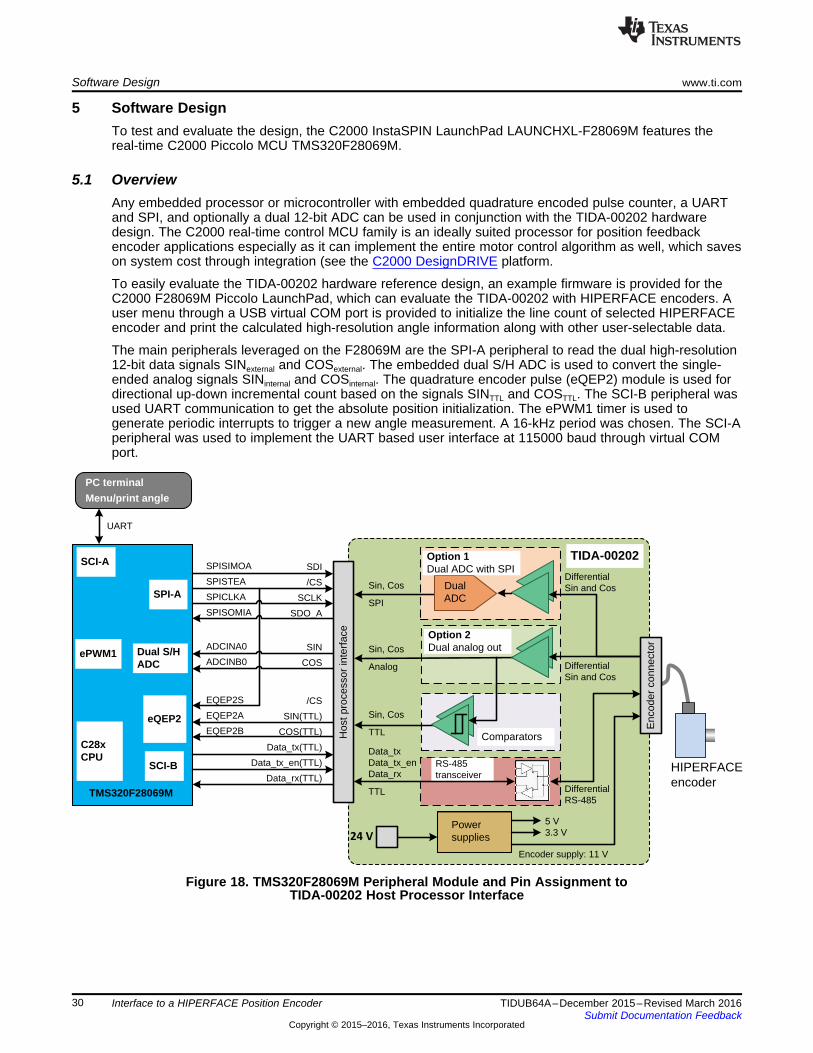
5 Software DesignTo test and evaluate the design, the C2000 InstaSPIN LaunchPad LAUNCHXL-F28069M features thereal-time C2000 Piccolo MCU TMS320F28069M.
5.1 OverviewAny embedded processor or microcontroller with embedded quadrature encoded pulse counter, a UARTand SPI, and optionally a dual 12-bit ADC can be used in conjunction with the TIDA-00202 hardwaredesign. The C2000 real-time control MCU family is an ideally suited processor for position feedbackencoder applications especially as it can implement the entire motor control algorithm as well, which saveson system cost through integration (see the C2000 DesignDRIVE platform.
To easily evaluate the TIDA-00202 hardware reference design, an example firmware is provided for theC2000 F28069M Piccolo LaunchPad, which can evaluate the TIDA-00202 with HIPERFACE encoders. Auser menu through a USB virtual COM port is provided to initialize the line count of selected HIPERFACEencoder and print the calculated high-resolution angle information along with other user-selectable data.
The main peripherals leveraged on the F28069M are the SPI-A peripheral to read the dual high-resolution12-bit data signals SINexternal and COSexternal. The embedded dual S/H ADC is used to convert the single-ended analog signals SINinternal and COSinternal. The quadrature encoder pulse (eQEP2) module is used fordirectional up-down incremental count based on the signals SINTTL and COSTTL. The SCI-B peripheral wasused UART communication to get the absolute position initialization. The ePWM1 timer is used togenerate periodic interrupts to trigger a new angle measurement. A 16-kHz period was chosen. The SCI-Aperipheral was used to implement the UART based user interface at 115000 baud through virtual COMport.
Figure 18. TMS320F28069M Peripheral Module and Pin Assignment toTIDA-00202 Host Processor Interface

Start
Init F28069 clocks, 16-kHz timer and peripherals
Init ADS7254Init F28069 ADC
Init global structures HiperfaceInput, HiperfaceOutput, UartData
Periodic interrupt?
UART user interface
ISR
Terminate program
End
No
Yes
Yes
No
Calculate absolute angle offset to eQEP using HIPERFACE digital connectionAbsolute position
known? No
Yes
www.ti.com Software Design
31TIDUB64A–December 2015–Revised March 2016Submit Documentation Feedback
Copyright © 2015–2016, Texas Instruments Incorporated
Interface to a HIPERFACE Position Encoder
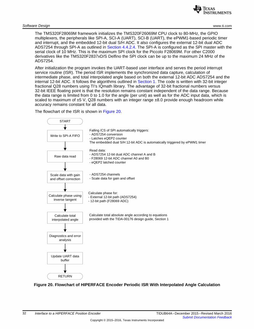
5.2 C2000 Piccolo FirmwareThe example firmware is developed and compiled for the Piccolo TMS320F28069M and leverages theperipheral modules outlined in Figure 18.
The firmware leverages C2000 controlSUITE™. The firmware basically consists of three functional blocks:• The F28069M framework, as outlined in Figure 19• The algorithm to synchronously sample the required data and calculate the interpolated angle• The UART terminal-based user interface
Figure 19. Flowchart of HIPERFACE Encoder F28069M Framework
START
Write to SPI-A FIFO
Raw data read
Scale data with gain and offset correction
RETURN
Falling /CS of SPI automatically triggers: - ADS7254 conversion - Latches eQEP2 counterThe embedded dual S/H 12-bit ADC is automatically triggered by ePWM1 timer
Read data: - ADS7254 12-bit dual ADC channel A and B- F28069 12-bit ADC channel A0 and B0- eQEP2 latched counter
- ADS7254 channels- Scale data for gain and offset
Calculate phase using inverse tangent
Calculate phase for:- External 12-bit path (ADS7254) - 12-bit path (F28069 ADC)
Calculate total interpolated angle
Calculate total absolute angle according to equations provided with the TIDA-00176 design guide, Section 1
Diagnostics and error analysis
Update UART data buffer
Software Design www.ti.com
32 TIDUB64A–December 2015–Revised March 2016Submit Documentation Feedback
Copyright © 2015–2016, Texas Instruments Incorporated
Interface to a HIPERFACE Position Encoder
The TMS320F28069M framework initializes the TMS320F26069M CPU clock to 80-MHz, the GPIOmultiplexers, the peripherals like SPI-A, SCI-A (UART), SCI-B (UART), the ePWM1-based periodic timerand interrupt, and the embedded 12-bit dual S/H ADC. It also configures the external 12-bit dual ADCADS7254 through SPI-A as outlined in Section 4.4.2.4. The SPI-A is configured as the SPI master with theserial clock of 10 MHz. This is the maximum SPI clock for the Piccolo F28069M. For other C2000derivatives like the TMS320F2837xD/S Delfino the SPI clock can be up to the maximum 24 MHz of theADS7254.
After initialization the program invokes the UART-based user interface and serves the period interruptservice routine (ISR). The period ISR implements the synchronized data capture, calculation ofintermediate phase, and total interpolated angle based on both the external 12-bit ADC ADS7254 and theinternal 12-bit ADC. It follows the algorithms outlined in Section 1. The code is written with 32-bit integerfractional Q28 numbers using TI’s IQmath library. The advantage of 32-bit fractional numbers versus32-bit IEEE floating point is that the resolution remains constant independent of the data range. Becausethe data range is limited from 0 to 1.0 for the angle (per unit) as well as for the ADC input data, which isscaled to maximum of ±5 V, Q28 numbers with an integer range ±8.0 provide enough headroom whileaccuracy remains constant for all data.
The flowchart of the ISR is shown in Figure 20.
Figure 20. Flowchart of HIPERFACE Encoder Periodic ISR With Interpolated Angle Calculation

Print Menu
µE¶?
Enter menu item
Basic display at 10 Hz: angle
µH¶? µD¶? µU¶?
Expert display at 10 Hz: angle, increment, phase
Return to Menu?
Return to Menu?
Print angle, increment, phase at 10 Hz
Return to Menu?
Print raw data sin, cos, QEP at 10 Hz
Return to Menu?
No
Yes
No
Yes
No
Yes
No
Yes
No
Yes
No
Yes
No
Yes
No
Yes
Start
Print Header
Enter HIPERFACE Encoder Linecount
Linecount entered?
Initialize eQEP2 moduleEnable 16-kHz periodic
interrupt
No
Yes
Align QEP module with HIPERFACE absolute position
value
Invert PIN function of COS signal
www.ti.com Software Design
33TIDUB64A–December 2015–Revised March 2016Submit Documentation Feedback
Copyright © 2015–2016, Texas Instruments Incorporated
Interface to a HIPERFACE Position Encoder
5.3 User InterfaceFor a quick evaluation, a virtual COM port-based user interface was implemented. Any terminal interfaceat 115000 baud like Tera Term can be used.
The user interface allows the user to enter the line count of the connected HIPERFACE encoder beforethe program reaches the main menu. The menu provides menu item options for the user to select either abasic display mode with just the high-resolution angle printed or an expert display mode, both with a10-Hz update rate. Other menu items are data dump modes at 10-Hz update rates, intended write to a filefor post analysis.
The flowchart of the user interface is shown in Figure 21.
Figure 21. Flowchart of UART Terminal User Interface

Software Design www.ti.com
34 TIDUB64A–December 2015–Revised March 2016Submit Documentation Feedback
Copyright © 2015–2016, Texas Instruments Incorporated
Interface to a HIPERFACE Position Encoder
Table 18 through Table 21 outline the data output format for each of the four menu items. In data dumpmode, a 'tab' is included as a delimiter between the data in each row.
Table 18. Basic Display Mode Output Format and Data Scaling
MENU COLUMN 1 COLUMN 2 COLUMN 3 COLUMN 4 COLUMN 5
‘b’ basic display Total angle withADS7254 (scale) — — — —
Data format Float (0 to 360degrees) — — — —
Table 19. Expert Display Mode Output Format and Data Scaling
MENU COLUMN 1 COLUMN 2 COLUMN 3 COLUMN 4 COLUMN 5
‘e’ expert display Total angle withADS7254 (scale)
Absolute positionfrom digital data Incremental count Phase ADS7254
(scale)
PhaseF28069M ADC(scale)
Data format Float (0 to 360degrees) Integer Integer Float (0 to 1.0) Float (0 to 1.0)
Table 20. Angle Data Dump Menu Format and Scaling
MENU COLUMN 1 COLUMN 2 COLUMN 3 COLUMN 4 COLUMN 5 COLUMN 6
‘d’ angle dump Total angle withADS7254 (scale)
Total angle withF28069 ADC(scale)
Incrementalcount
Phase ADS7254(scale)
PhaseF28069M ADC(scale)
Periodic tick(scale)
Data format Float (0 to 360degrees)
Float (0 to 360degrees) Integer Float (0 to 1.0) Float (0 to 1.0) Integer (66 µs)
Table 21. Raw Data Dump Menu Format and Scaling
MENU COLUMN 1 COLUMN 2 COLUMN 3 COLUMN 4 COLUMN 5 COLUMN 6 COLUMN 7
‘r’ raw data Incrementalcount (SW)
Incrementalcount (latch on/CS)
InputSIN+/SIN–,ADS7254(scale)
InputCOS+/COS–,ADS7254(scale)
InputSIN+/SIN–,F28069(scale)
InputCOS+/COS–,F28069(scale)
Periodic tick(scale)
Integer Integer Float (VPP) Float (VPP) Float (VPP) Float (VPP) Integer (66 µs)
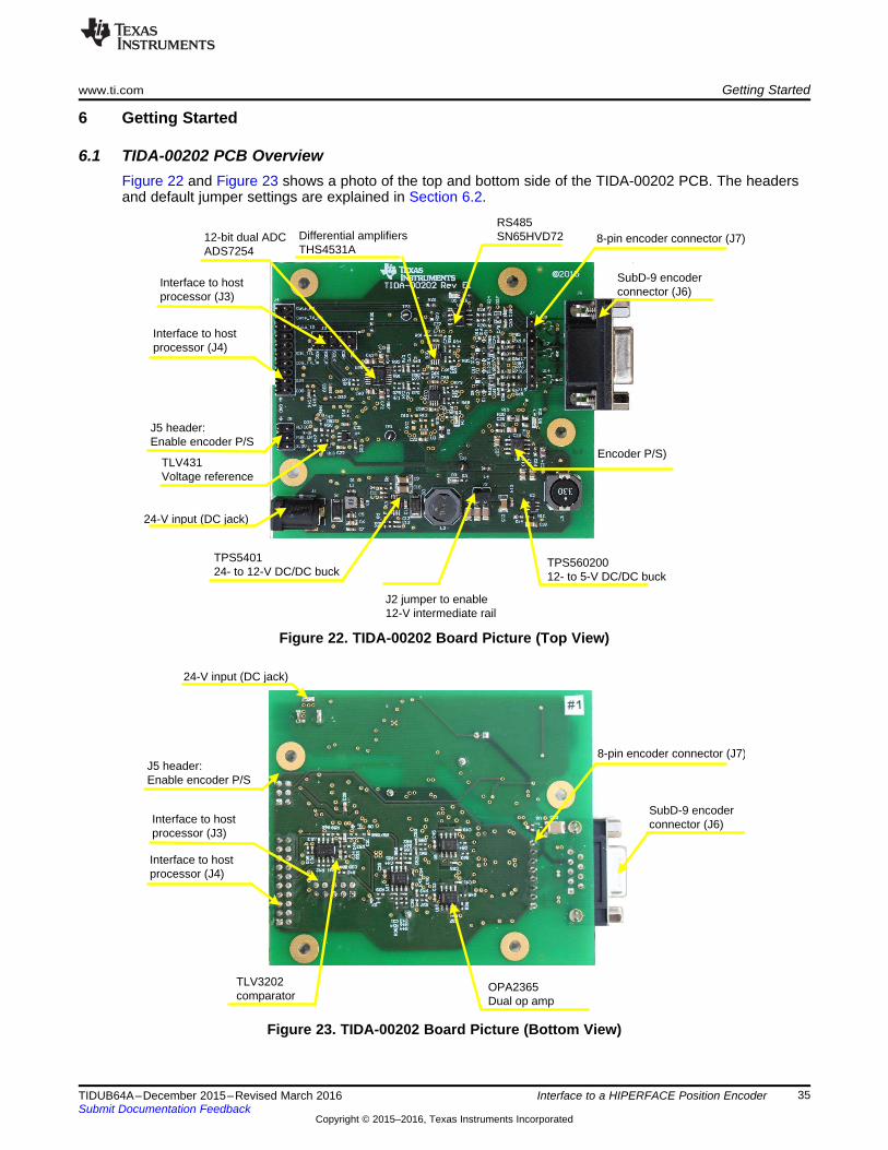
24-V input (DC jack)
Interface to host processor (J4)
TLV3202comparator
J5 header:Enable encoder P/S
SubD-9 encoder connector (J6)
8-pin encoder connector (J7)
OPA2365Dual op amp
Interface to host processor (J3)
12-bit dual ADCADS7254
24-V input (DC jack)
Encoder P/S)
Interface to host processor (J4)
TPS540124- to 12-V DC/DC buck
J5 header:Enable encoder P/S
SubD-9 encoder connector (J6)
8-pin encoder connector (J7)RS485SN65HVD72
J2 jumper to enable 12-V intermediate rail
TPS56020012- to 5-V DC/DC buck
Differential amplifiersTHS4531A
Interface to host processor (J3)
TLV431Voltage reference
www.ti.com Getting Started
35TIDUB64A–December 2015–Revised March 2016Submit Documentation Feedback
Copyright © 2015–2016, Texas Instruments Incorporated
Interface to a HIPERFACE Position Encoder
6 Getting Started
6.1 TIDA-00202 PCB OverviewFigure 22 and Figure 23 shows a photo of the top and bottom side of the TIDA-00202 PCB. The headersand default jumper settings are explained in Section 6.2.
Figure 22. TIDA-00202 Board Picture (Top View)
Figure 23. TIDA-00202 Board Picture (Bottom View)
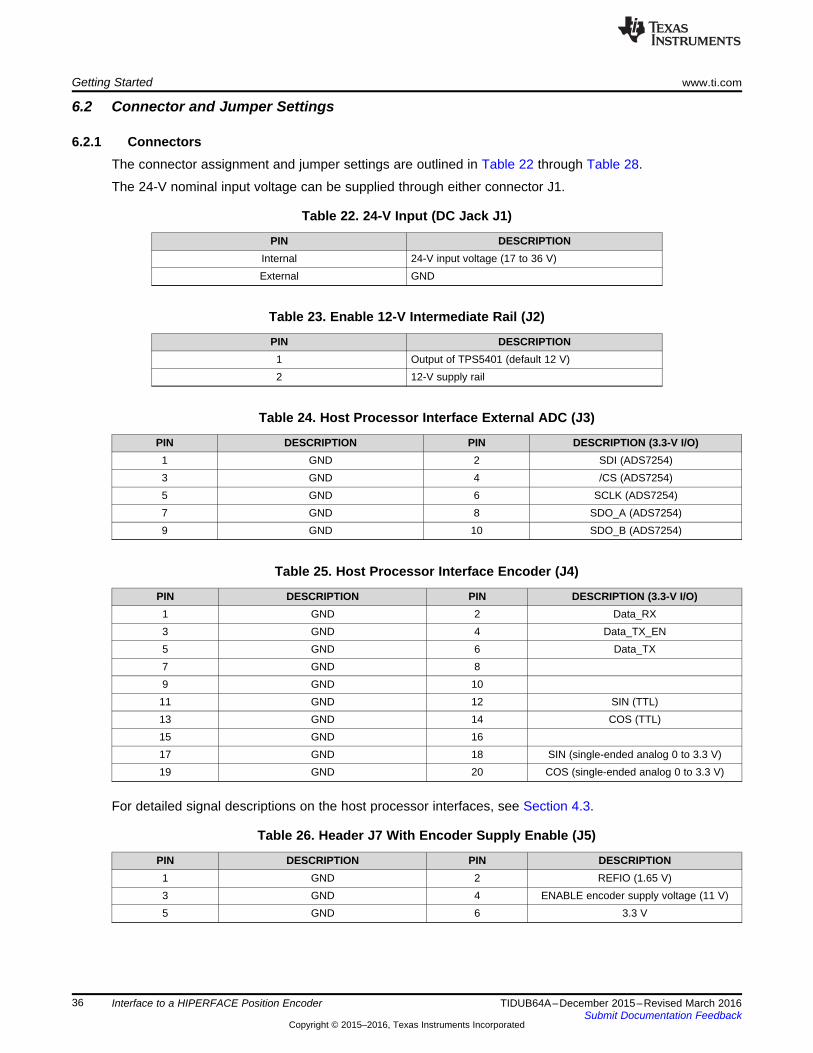
Getting Started www.ti.com
36 TIDUB64A–December 2015–Revised March 2016Submit Documentation Feedback
Copyright © 2015–2016, Texas Instruments Incorporated
Interface to a HIPERFACE Position Encoder
6.2 Connector and Jumper Settings
6.2.1 ConnectorsThe connector assignment and jumper settings are outlined in Table 22 through Table 28.
The 24-V nominal input voltage can be supplied through either connector J1.
Table 22. 24-V Input (DC Jack J1)
PIN DESCRIPTIONInternal 24-V input voltage (17 to 36 V)External GND
Table 23. Enable 12-V Intermediate Rail (J2)
PIN DESCRIPTION1 Output of TPS5401 (default 12 V)2 12-V supply rail
Table 24. Host Processor Interface External ADC (J3)
PIN DESCRIPTION PIN DESCRIPTION (3.3-V I/O)1 GND 2 SDI (ADS7254)3 GND 4 /CS (ADS7254)5 GND 6 SCLK (ADS7254)7 GND 8 SDO_A (ADS7254)9 GND 10 SDO_B (ADS7254)
Table 25. Host Processor Interface Encoder (J4)
PIN DESCRIPTION PIN DESCRIPTION (3.3-V I/O)1 GND 2 Data_RX3 GND 4 Data_TX_EN5 GND 6 Data_TX7 GND 89 GND 1011 GND 12 SIN (TTL)13 GND 14 COS (TTL)15 GND 1617 GND 18 SIN (single-ended analog 0 to 3.3 V)19 GND 20 COS (single-ended analog 0 to 3.3 V)
For detailed signal descriptions on the host processor interfaces, see Section 4.3.
Table 26. Header J7 With Encoder Supply Enable (J5)
PIN DESCRIPTION PIN DESCRIPTION1 GND 2 REFIO (1.65 V)3 GND 4 ENABLE encoder supply voltage (11 V)5 GND 6 3.3 V

www.ti.com Getting Started
37TIDUB64A–December 2015–Revised March 2016Submit Documentation Feedback
Copyright © 2015–2016, Texas Instruments Incorporated
Interface to a HIPERFACE Position Encoder
Table 27. Encoder Sub-D9 Connector (J6)
PIN DESCRIPTION PIN DESCRIPTION1 RS485+ 2 Encoder supply GND3 SIN– 4 Encoder supply VCC (default 11 V)5 COS+ 6 RS485–7 NC 8 SIN+9 COS–
Table 28. Encoder 8SIL100 Connector (J7)
PIN DESCRIPTION PIN DESCRIPTION1 RS485– 2 RS485+3 Encoder supply GND 4 SIN–5 SIN+ 6 Encoder supply VCC (default 11 V)7 COS– 8 COS+
6.2.2 Default Jumpers ConfigurationPrior to working with the TIDA-00202 board, ensure the following default jumper settings are applied.Refer to the board picture in Figure 24.
Table 29. Default Jumpers Settings
HEADER JUMPER SETTINGJ2 Insert a jumper between J32 pins 1-2 to enable the 12-V intermediate rail connected to the POL.
6.3 Design Evaluation
6.3.1 PrerequisitesThe following hardware equipment and software are required to evaluate the TIDA-00202 TI Design.
Table 30. Prerequisites
EQUIPMENT COMMENT
24-V power supply 24-V output power brick with at least 250-mA output currentOutput connector 2.1-mm I.D. × 5.5-mm O.D. × 9.5-mm Female
TIDA-00202 hardware For default jumper settings per Section 6.2.1 jumper for board settings 2 pins, 100 milsTIDA-00202 firmware Download from TIDA-00202 design folderInstaSPIN-MOTION F28069M Launchpad Available through TI eStoreUSB cable Mini USB type A to USB type A cableTIDA-00202 to LaunchPad adapter Internal TI (optional)Code Composer Studio™ 6 (CCS6) Download from www.ti.comPC terminal program Any terminal program, like for example Tera TermHIPERFACE Encoder For example, SRS50-HWA0-K21
Getting Started www.ti.com
38 TIDUB64A–December 2015–Revised March 2016Submit Documentation Feedback
Copyright © 2015–2016, Texas Instruments Incorporated
Interface to a HIPERFACE Position Encoder
6.3.2 Hardware SetupThe following connections are required between the TIDA-00202 and the InstaSPIN-MOTION LaunchPad.
Table 31. TIDA-00202 Host Processor Interface (J4) to InstaSPIN LaunchPad
TIDA-00202 HOST PROCESSOR INTERFACE (J6) CONNECT TO→
INSTASPIN-MOTION LAUNCHPADJ4 PIN DESCRIPTION HEADER PIN DESCRIPTION (3.3-V I/O)
1 GND J3-Pin 22 GND19 GND J2-Pin 20 GND2 Data_RX J2-Pin 18 GPIO44/SCIRXDB4 Data_TX_EN J1-Pin 9 GPIO336 Data_TX J1-Pin 8 GPIO22/ SCITXDB8 NC NC NC
10 NC NC NC12 SIN (TTL) J6-Pin 55 GPIO24/eQEP2A14 COS (TTL) J6-Pin 54 GPIO25/eQEP2B16 NC NC NC
18 SIN (single-ended analog0 to 3.3 V) J3-Pin 27 ADCIN_A0
20 COS (single-ended analog0 to 3.3 V) J3-Pin 28 ADCIN_B0
Table 32. TIDA-00202 External ADC Interface (J3) to InstaSPIN LaunchPad
TIDA-00202 HOST PROCESSOR INTERFACE (J6) CONNECT TO→
INSTASPIN-MOTION LAUNCHPADJ3 PIN DESCRIPTION HEADER PIN DESCRIPTION (3.3-V I/O)
1 GND J3-Pin 22 GND3 GND J2-Pin 20 GND2 SDI (ADS7254) J2-Pin 15 GPIO16/SPISIMOA
4 /CS (ADS7254) J2-Pin 19J6-Pin 59
GPIO27/eQEP2SGPIO19/SPISTEA
6 SCLK (ADS7254) J1-Pin 7 GPIO18/SPICLKA8 SDO_A (ADS7254) J2-Pin 14 GPIO17/SPISOMIA
10 SDO_B (ADS7254) NC NC NC

www.ti.com Getting Started
39TIDUB64A–December 2015–Revised March 2016Submit Documentation Feedback
Copyright © 2015–2016, Texas Instruments Incorporated
Interface to a HIPERFACE Position Encoder
Follow these steps to setup the hardware:1. Connect the TIDA-00202 board with the InstaSPIN-MOTION LaunchPad using the proper connections
as shown above. Note: For the internal testing, an adapter board has been designed to interfacebetween the TIDA-00202 and the InstaSPIN-MOTION LaunchPad, as shown in Figure 24.
2. Verify the TIDA-00202 is configured with the default jumper settings as per Section 6.2.2.3. Connect the HIPERFACE encoder to the board by using either the SubD-9 connector (J6) or the SIL-8
connector (J7).4. Insert the 24-V input from the power brick in the J1 connector.5. Connect the USB mini cable from the InstaSPIN-MOTION LaunchPad to the PC.
Figure 24. TIDA-00202 Board Mounted on the InstaSPIN-MOTION LaunchPad (Top View)
Figure 25. TIDA-00202 Board Mounted on the InstaSPIN-MOTION LaunchPad (Bottom View)
Please also refer to the InstaSPIN-MOTION LaunchPad prerequisites at http://www.ti.com/tool/launchxl-f28069m.
Ensure the following jumpers on the F28069 LaunchPad are set: JP1, JP2, JP3, and JP7. Do not set JP4,JP5, and JP6 as these must not be connected.

Getting Started www.ti.com
40 TIDUB64A–December 2015–Revised March 2016Submit Documentation Feedback
Copyright © 2015–2016, Texas Instruments Incorporated
Interface to a HIPERFACE Position Encoder
6.3.3 Software SetupFollow these steps to setup the software:1. If not done, download the TIDA-00202 HIPERFACE Encoder Firmware from the TIDA-00202 design
folder and extract (for example, to folder c:\ti\tida-00202\bin).2. Invoke a Terminal program like Tera Term that can connect to the corresponding virtual COM port of
the InstaSPIN-MOTION F28069M LaunchPad.3. Setup the Terminal program in Serial Console mode and set the parameters to:
Baud Rate = 115200, Data = 8-bit, Parity = None, Stop = 1-bit, Flow Control = None4. Launch CCS.5. In CCS, setup the XDS100 JTAG target with the InstaSPIN-MOTION F28069M LaunchPad.6. In CCS, connect to the TMS320F28069M and download TIDA-00202 binary output file:
Run → Load Program → TIDA-00202_HIPERFACEEncoder_Example_Firmware_rev1_0.out7. In CCS, run the target.
The terminal program should display the start screen of TIDA-00202 as shown in Figure 26.
NOTE: After the binary file has been loaded to the F28069M, Steps 4 through 7 are not requiredanymore. Simply reset the LaunchPad to restart the program. Ensure the F28069M isconfigured to boot from internal flash. Refer to the InstaSPIN-MOTION LaunchPaddocumentation.
To troubleshoot, if no connection is established, the VCP driver of the USB virtual Com port TI XDS100Channel B needs to be enabled under Windows 7 Device Manager. For more details, refer to theInstaSPIN-MOTION LaunchPad documentation.
Figure 26. TIDA-00202 User Interface at Startup

www.ti.com Getting Started
41TIDUB64A–December 2015–Revised March 2016Submit Documentation Feedback
Copyright © 2015–2016, Texas Instruments Incorporated
Interface to a HIPERFACE Position Encoder
6.3.4 User InterfaceAfter startup, the user interface requires to enter the HIPERFACE encoder line count in decimal. After theline count is entered, the main menu is available, as shown in Figure 27.
Figure 27. TIDA-00202 User Interface Main Menu
Four menus are available. Each can be selected by pressing the characters 'b', 'e', 'r', or 'a'. The menuitem x is reserved for internal test modes during software development.
Press 'b' or 'e' to select the basic or expert display mode, which will print the interpolated angle in degreesor additional information. Note that the software is to test the board; sometimes the HIPERFACE digitaldata is not being transferred correctly, which can delay the absolute digital value. To return to the mainmenu, press any key.
Figure 28. Basic Angle Display and Expert Display Mode

Getting Started www.ti.com
42 TIDUB64A–December 2015–Revised March 2016Submit Documentation Feedback
Copyright © 2015–2016, Texas Instruments Incorporated
Interface to a HIPERFACE Position Encoder
Press 'a' to start an angle data dump at a 10-Hz update rate. The data format is as outlined in Section 5. Ascreenshot is shown in Figure 29. Press any key to stop and return to the main menu.
Figure 29. Angle Dump Mode at 10-Hz Update Rate
Press 'r' to start a raw data dump at a 10-Hz update rate. The data format is as outlined in Section 5. Ascreenshot is shown in Figure 30. Press any key to stop and return to the main menu.
Figure 30. Raw Data Dump Mode at 10-Hz Update Rate

www.ti.com Test Results
43TIDUB64A–December 2015–Revised March 2016Submit Documentation Feedback
Copyright © 2015–2016, Texas Instruments Incorporated
Interface to a HIPERFACE Position Encoder
7 Test ResultsTests were done to characterize each individual functional block as well as the entire board. In particular,the following tests were conducted:• Analog signal chain performance• RS-485 based digital signal performance• Power management• System performance with HIPERFACE sin/cos emulation and HIPERFACE encoder
Tests were done at room temperature around 22°C to 23°C. The following equipment were used for theTIDA-00202 testing session:
Table 33. Test Equipment for TIDA-00202 Performance Tests
TEST EQUIPMENT PART NUMBERProgrammable 16-bit waveform generator Keysight (Agilent) 33600ALow-speed oscilloscope (suitable for power supply tests) Tektronix TDS2024BHigh-speed oscilloscope (suitable for analog signal tests) Tektronix TDS784CAdjustable SMPS Knuerr-Heinzinger Polaris 125-524 V at 2.5-A SMPS (power brick) V-infinity 3A-621DN24True RMS multimeter Fluke 179Differential probes Tektronix P6630Single ended probes Tektronix P6139AProgrammable thermal chamber Voetsch VT 4002Programmable electronic load module Chroma 63103Control module for electronic load module Chroma 6314Sick shielded cable, M23, female/wires, 30 m DOL-2308-G30MJB2Sick shielded cable, M23, female/wires, 3 m DOL-2308-G03MJB2SICK HIPERFACE Encoders SRS50-HWA0-K21

SIN+
SIN-
COS+
COS-
ADS7254
ADC
ADC
SPI (A, B)
THS4531A
Host processor interface ± external ADC (J3)
Encoder connector (J7)
Test signal inputTest point 1 (analog)Test point 2 (digital)
Test Results www.ti.com
44 TIDUB64A–December 2015–Revised March 2016Submit Documentation Feedback
Copyright © 2015–2016, Texas Instruments Incorporated
Interface to a HIPERFACE Position Encoder
7.1 Analog Performance TestsFigure 31 shows a picture of the TIDA-00202 analog signal chain tests.
Figure 31. Test Setup for TIDA-00202 Analog Signal Chain Performance Tests
Both the 12-bit signal path featuring fully differential amplifiers THS4531A and the dual 12-bit ADCADS7253 as well as the differential to single-ended analog signal path were tested. For this design’spurpose, a dual output programmable function generator was used. The inputs signals are applied atconnector J7 (differential inputs SIN and COS). The output waveforms have been collected at differentprobe points, depending on the signal path that was analyzed.
7.1.1 12-Bit Dual ADC Signal Path With SPI OutputThe measurements have been taken on the high-precision, high-resolution signal path. A sinusoidal signalwith 1 VPP was injected at the encoder connector J7 inputs SIN+, SIN– and COS+, COS–, and thedifferential analog signals was measured at the ADS7254 differential inputs. Figure 32 outlines the inputand output signals measured for the test.
Figure 32. 12-Bit Dual ADC With SPI Signal Chain Measurement Points
Figure 33 shows the magnitude and phase response, which is mainly defined by the THS4531A gainsetting of 2, the passive first order low-pass filter comprised of two 10-Ω series resistors, and the 2.2-nFparallel capacitor.

Frequency (Hz)
Pha
se
Gai
n (d
B)
-20
-10
0
10
20
1 10 100 1k 10k 100k 1M-180°
-135°
-90°
-45°
0°
D001
Phase with L = 47 PHGain with L = 47 PHPhase with L = 0 PHGain with L = 0 PH
www.ti.com Test Results
45TIDUB64A–December 2015–Revised March 2016Submit Documentation Feedback
Copyright © 2015–2016, Texas Instruments Incorporated
Interface to a HIPERFACE Position Encoder
7.1.1.1 Bode Plot of Analog Path From Encoder Connector to ADS7254 InputFigure 33 shows the bode plot for the option with the optional series 47-µH inductors and without. In thelatter option, 0-Ω resistors were used instead of the 47-µH inductors.
Figure 33. Bode Plot for the High-Resolution Analog from the Encoder Differential Input to the ADS7254Differential Input (Channel SIN)
7.1.1.2 FFT Performance Plots for Entire 12-Bit Fully Differential Signal PathFor the following tests, the entire high-resolution signal chain, featuring the differential amplifier THS4531Aconnected through an RC filter to the dual 12-bit ADC ADS7254, has been tested. A sinusoidal test signalhas been injected at the encoder differential input pins, and the 12-bit digital data has been analyzed.
The analysis has been done in the frequency domain to evaluate the performance on signal-to-noise ratio(SNR), total harmonic distortions (THD), signal-to-noise And distortion (SINAD), and effective number ofbits (ENOB).
For the test a 1-kHz sine wave at an amplitude of 1 VPP was used, which represents the typical sine andcosine differential output of the HIPERFACE encoders. This input signal is applied to one of the inputchannels, SIN+,SIN– or COS+,COS–, at a time, while the other channel was left unconnected. Thepurpose is to measure for crosstalk and zero-input noise level between the two channels SIN and COS.
Both channels SIN and COS were sampled at 16 kHz, and 8192 consecutive 12-bit samples wereacquired for each channel. The DFT has been calculated for the collected data to measure the SNR andTHD.
The Blackman-Harris windowing function was used to weigh the 8192 samples prior to the 8192 FFT.
The following figures show the DFT of the entire high-resolution channel with a sinusoidal input voltage of1-VPP amplitude and 1 kHz, which is half the full-scale input of 2 VPP.
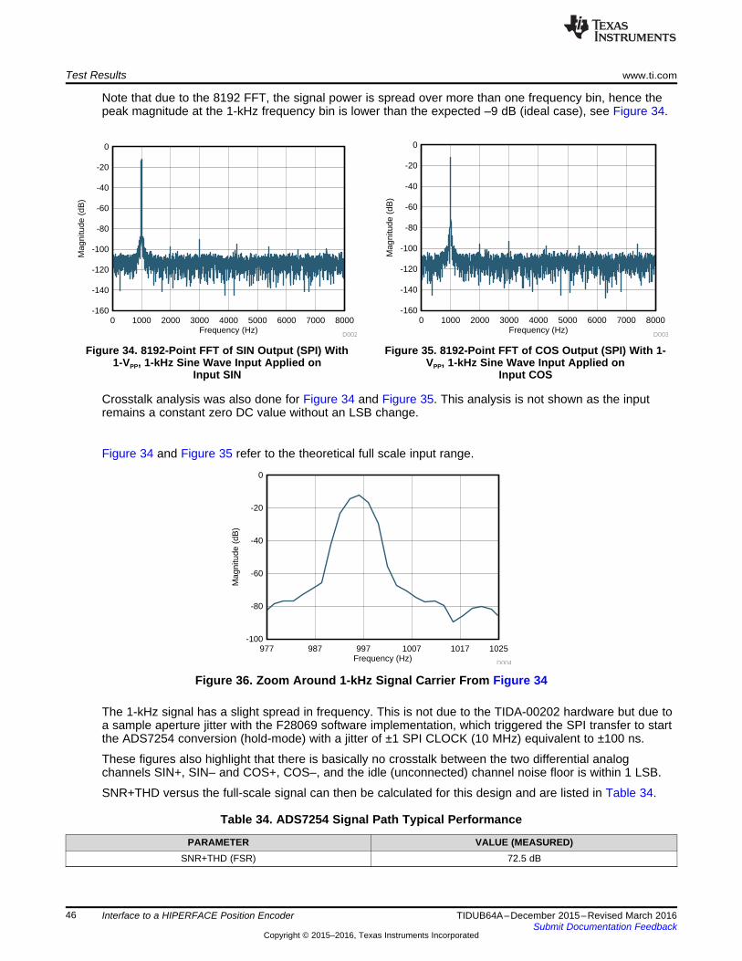
Frequency (Hz)
Mag
nitu
de (
dB)
977 987 997 1007 1017 1025-100
-80
-60
-40
-20
0
D004
Frequency (Hz)
Mag
nitu
de (
dB)
0 1000 2000 3000 4000 5000 6000 7000 8000-160
-140
-120
-100
-80
-60
-40
-20
0
D002Frequency (Hz)
Mag
nitu
de (
dB)
0 1000 2000 3000 4000 5000 6000 7000 8000-160
-140
-120
-100
-80
-60
-40
-20
0
D003
Test Results www.ti.com
46 TIDUB64A–December 2015–Revised March 2016Submit Documentation Feedback
Copyright © 2015–2016, Texas Instruments Incorporated
Interface to a HIPERFACE Position Encoder
Note that due to the 8192 FFT, the signal power is spread over more than one frequency bin, hence thepeak magnitude at the 1-kHz frequency bin is lower than the expected –9 dB (ideal case), see Figure 34.
Figure 34. 8192-Point FFT of SIN Output (SPI) With1-VPP, 1-kHz Sine Wave Input Applied on
Input SIN
Figure 35. 8192-Point FFT of COS Output (SPI) With 1-VPP, 1-kHz Sine Wave Input Applied on
Input COS
Crosstalk analysis was also done for Figure 34 and Figure 35. This analysis is not shown as the inputremains a constant zero DC value without an LSB change.
space
Figure 34 and Figure 35 refer to the theoretical full scale input range.
Figure 36. Zoom Around 1-kHz Signal Carrier From Figure 34
The 1-kHz signal has a slight spread in frequency. This is not due to the TIDA-00202 hardware but due toa sample aperture jitter with the F28069 software implementation, which triggered the SPI transfer to startthe ADS7254 conversion (hold-mode) with a jitter of ±1 SPI CLOCK (10 MHz) equivalent to ±100 ns.
These figures also highlight that there is basically no crosstalk between the two differential analogchannels SIN+, SIN– and COS+, COS–, and the idle (unconnected) channel noise floor is within 1 LSB.
SNR+THD versus the full-scale signal can then be calculated for this design and are listed in Table 34.
Table 34. ADS7254 Signal Path Typical Performance
PARAMETER VALUE (MEASURED)SNR+THD (FSR) 72.5 dB

Analog Input Frequency (Hz)
Pha
se
Gai
n (d
B)
-20
-10
0
10
20
1 10 100 1k 10k 100k 1M
0°
-45°
-90°
-135°
-180°
D005
Phase with L = 47 PHGain with L = 47 PHPhase with L = 0 PHGain with L = 0 PH
www.ti.com Test Results
47TIDUB64A–December 2015–Revised March 2016Submit Documentation Feedback
Copyright © 2015–2016, Texas Instruments Incorporated
Interface to a HIPERFACE Position Encoder
7.1.2 Differential to Single-Ended Analog Signal Path
7.1.2.1 Bode PlotThe bode plot is shown for the option with the optional series 47-µH inductors and without. In the latteroption, 0-Ω resistors were used instead of the 47-µH inductors.
Figure 37. Bode Plot for Differential to Single-Ended Analog Signal Path (Channel SIN)

Frequency (Hz)
Mag
nitu
de (
dB)
0 1000 2000 3000 4000 5000 6000 7000 8000-140
-120
-100
-80
-60
-40
-20
D008Frequency (Hz)
Mag
nitu
de (
dB)
0 1000 2000 3000 4000 5000 6000 7000 8000-160
-140
-120
-100
-80
-60
-40
-20
0
D009
Frequency (Hz)
Mag
nitu
de (
dB)
0 1000 2000 3000 4000 5000 6000 7000 8000-160
-140
-120
-100
-80
-60
-40
-20
0
D006Frequency (Hz)
Mag
nitu
de (
dB)
0 1000 2000 3000 4000 5000 6000 7000 8000-160
-140
-120
-100
-80
-60
-40
-20
D007
Test Results www.ti.com
48 TIDUB64A–December 2015–Revised March 2016Submit Documentation Feedback
Copyright © 2015–2016, Texas Instruments Incorporated
Interface to a HIPERFACE Position Encoder
7.1.2.2 FFT Performance Plots for Single-Ended Analog Output Path
Figure 38. 8192-Point FFT of SIN Output (C2000 ADC)With 1-VPP, 1-kHz Sine Wave Input Applied on Input SIN
Figure 39. 8192-Point FFT of COS Output (C2000 ADC)With 1-VPP, 1-kHz Sine Wave Input Applied on Input SIN
Figure 40. 8192-Point FFT of SIN Output (C2000 ADC)With 1-VPP, 1-kHz Sine Wave Input Applied on Input COS
Figure 41. 8192-Point FFT of COS Output (C2000 ADC)With 1-VPP, 1-kHz Sine Wave Input Applied on Input COS
SNR+THD versus the full-scale signal can then be calculated for this design and are listed in Table 35.
Table 35. TMS320F28069 Signal Path Typical Performance
PARAMETER VALUE (MEASURED)SNR + THD (FSR) 69 dB
7.1.3 Comparator Subsystem With Digital Output Signals SINTTL and COSTTL
In this section, the performance of the comparator with hysteresis that converts the single-ended analogsignals SIN and COS into digital signals was tested.
The focus was on the propagation delay of the comparator output signals SINTTL and COSTTL at the hostconnector J4 versus the analog input at the ADS7254 for the high-resolution path as well as the single-ended analog signals for the analog path.
The aim of the test was to measure the overall signal delay of the comparator path versus the analogpath, considering the delays introduced by hysteresis, phase shift due to low-pass filtering, and thepropagation delay of the comparator itself.

Sin ADC7254 analog signal
Sin C2k analog signal
Sin TTL signal
Sin ADC7254 analog signal
Sin C2k analog signal
Sin TTL signal
www.ti.com Test Results
49TIDUB64A–December 2015–Revised March 2016Submit Documentation Feedback
Copyright © 2015–2016, Texas Instruments Incorporated
Interface to a HIPERFACE Position Encoder
Since both channels SIN and COS were done absolutely symmetrical with regards to the comparatoroutput, measurements have only been conducted with the SIN channel.
The analog signals were both measured with a single-ended probe, hence on the differential input of theADS7254 only the positive differential signal was measured versus GND.
For the test, sinusoidal input signals were injected at the encoder connector J7, SIN_P, SIN_M andCOS_P, COS_M.
For the signal path, the amplitude of the input signal was set to 1.0 VPP with a frequency of 100 Hz and150 kHz (maximum) to test the worst case scenario for the propagation delay.
Test results are shown in the following figures. Note that both the high-resolution path (at the differentialinput of the ADS7254) and the single-ended analog path (at connector J4 Pin 12) are compared to thecomparator output (at connector J4 Pin 18).
Figure 42. Comparator Output SINTTL versus Differential Input to ADS7254 and Analog Output SIN (J4-12)With Input 1.0 VPP, 100 Hz at Encoder Connector J7-4, J7-5
Figure 43. Comparator Output SINTTL versus Differential Input to ADS7254 and Analog Output SIN (J4-12)With Input 1.0 VPP, 150 kHz at Encoder Connector J7-4, J7-5

Test Results www.ti.com
50 TIDUB64A–December 2015–Revised March 2016Submit Documentation Feedback
Copyright © 2015–2016, Texas Instruments Incorporated
Interface to a HIPERFACE Position Encoder
As expected, the maximum overall phase shift including RC filter decoupling networks occurs at 150 kHzis total around 276 ns, equal to 15 degrees, hence well below the 30 degrees per specification inSection 2. The very low propagation delay of the TLV3202 with typically 40 ns has a major impact on thislow number. This also gives a major margin to compensate all the possible spreads in the parametersinfluencing the amount of phase delay due to low-pass filters, and especially a larger margin on the hostMCU with regards to synchronized sampling of the analog signals versus the incremental counter.
The propagation delay at 100 Hz is almost the same than for the high-resolution channel because thedelay at lower frequencies is dominated by the amplitude-dependent hysteresis.
In a second step, only the delay related to the comparator with hysteresis was measured. The delay wasspecified as the input to the comparator (analog signal at R41) and the output of the comparator.
The delay introduced by the comparator block only (hysteresis and comparator propagation delay) hasbeen measured and is listed in Table 36.
Table 36. Hysteresis Comparator Subsystem Delay
INPUT AT ENCODERCONNECTOR
VOLTAGE AT COMPARATORINPUT (SUCH AS R41) PROPAGATION DELAY PHASE DELAY
1.0 VPP, 100Hz 1.67 V 180 µs 6.5 degrees1.0 VPP, 150 kHz 0.9 V 276 ns 14.9 degrees

www.ti.com Test Results
51TIDUB64A–December 2015–Revised March 2016Submit Documentation Feedback
Copyright © 2015–2016, Texas Instruments Incorporated
Interface to a HIPERFACE Position Encoder
7.2 Digital Parameter Channel Performance Tests
7.2.1 RS-485 Eye Diagrams versus Cable LengthThe following figures show the eye diagrams using random NRZ data measured differentially with 130-Ω termination at the cable end (slavereceive side) with a differential Tektronix probe. The master transmitter clock rate was connected to channel 1 of the scope to trigger sampling ofthe differential data at the far cable end. The master clock was measured single ended at the input of the master RS-485 clock transmitter and isshown as reference (Ch1, 5 V/div, 25 ns) on the scope plots as well.
Measurements were conducted at cable lengths of 33 m and 3 m with maximum data rates as well as with the maximum rate specified perHIPERFACE for the HVD72.
Measurements at 33-m Cable Length Measurements at 3-m Cable Length
Figure 44. Eye Diagram HVD72, 33-m Cable Data Rate 38.4 kbaud Figure 45. Eye Diagram HVD72, 3-m Cable Data Rate 38.4 kbaud

Differential TX data
TX data from transceiver
Differential RX data
RX data from transceiver
Data-
Data+
Test Results www.ti.com
52 TIDUB64A–December 2015–Revised March 2016Submit Documentation Feedback
Copyright © 2015–2016, Texas Instruments Incorporated
Interface to a HIPERFACE Position Encoder
7.2.2 RS-485 Transceiver Propagation Delay and Differential Output LevelsFigure 46 shows the transmit data levels measured single-ended versus GND at the HIPERFACE SubD-9connector pins Data+ and Data– with a 3-m cable and 1230-Ω parallel termination at the far end. The highlevel is around 2.8 V and the low level around 0.8 V. When comparing with the datasheet, this is around15% lower. The reason is that in transmit direction the 10-Ω pulse proof resistors between the outputterminals COS and SIN parallel termination impedance form a voltage divider with a factor of 122 Ω/142Ω, which is approximately 0.86.
Figure 46. Voltage versus GND Connector J7 Terminals DATA+ and DATA– in Data Transmit Mode
Figure 47 and Figure 48 show the rise and fall time propagation delay of the SN65HVD72 RS-485transceiver driver and receiver with 122-Ω parallel termination. Note the different time scale for driver andreceiver measurement. The driver propagation delay measured is around 0.7 µs, the receiver propagationdelay is around 75 ns.
Figure 47. SN65HVD72 Propagation Delay for the Driver Figure 48. SN65HVD72 Propagation Delay for theReceiver
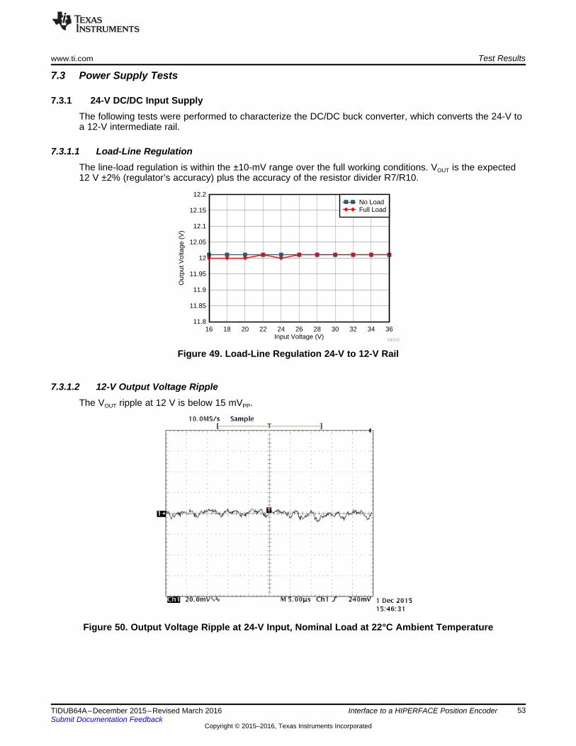
Input Voltage (V)
Out
put V
olta
ge (
V)
16 18 20 22 24 26 28 30 32 34 3611.8
11.85
11.9
11.95
12
12.05
12.1
12.15
12.2
D010
No LoadFull Load
www.ti.com Test Results
53TIDUB64A–December 2015–Revised March 2016Submit Documentation Feedback
Copyright © 2015–2016, Texas Instruments Incorporated
Interface to a HIPERFACE Position Encoder
7.3 Power Supply Tests
7.3.1 24-V DC/DC Input SupplyThe following tests were performed to characterize the DC/DC buck converter, which converts the 24-V toa 12-V intermediate rail.
7.3.1.1 Load-Line RegulationThe line-load regulation is within the ±10-mV range over the full working conditions. VOUT is the expected12 V ±2% (regulator’s accuracy) plus the accuracy of the resistor divider R7/R10.
Figure 49. Load-Line Regulation 24-V to 12-V Rail
7.3.1.2 12-V Output Voltage RippleThe VOUT ripple at 12 V is below 15 mVPP.
Figure 50. Output Voltage Ripple at 24-V Input, Nominal Load at 22°C Ambient Temperature

Load Current (mA)
Out
put V
olta
ge (
V)
0 25 50 75 100 125 150 175 200 225 25011
11.05
11.1
11.15
11.2
11.25
11.3
11.35
11.4
11.45
11.5
D011
Test Results www.ti.com
54 TIDUB64A–December 2015–Revised March 2016Submit Documentation Feedback
Copyright © 2015–2016, Texas Instruments Incorporated
Interface to a HIPERFACE Position Encoder
7.3.2 Encoder Power Supply Output VoltageThe output voltage of the LDO providing the supply for the encoder is well regulated and meets the specrequirements, as for the measurements in Figure 51.
Figure 51. Encoder Power Supply Output Voltage versus Load Current (0 to 250 mA)
The LDO has a shutdown mode when excess current is drawn from the device. Figure 52 shows theshutdown when a short circuit is done on the output.
Figure 52. Shutdown of the Encoder Power Supply During a Short Circuit
This feature can be used with the error pin to detect a short circuit and turn off the encoder power supplyfrom the processor. For more details on this option, see the LP2954 datasheet (SNVS096).

www.ti.com Test Results
55TIDUB64A–December 2015–Revised March 2016Submit Documentation Feedback
Copyright © 2015–2016, Texas Instruments Incorporated
Interface to a HIPERFACE Position Encoder
7.3.3 5-V and 3.3-V Point-of-LoadThe following tests were performed to characterize the DC/DC buck converter, which converts the 12-V toa 5-V rail directly.
7.3.3.1 Output Voltage Regulation
Table 37. Measured Output Voltage
SPECIFIED OUTPUT VOLTAGE MEASURED VOLTAGE CURRENT5 V 5.02 V 0 mA5 V 5.00 V 400 mA
7.3.3.2 5-V Output Voltage Ripple
Figure 53. Output Voltage Ripple at 5-V Input at Light Load 25 mA at 22°C Ambient Temperature
The ripple is due to the low power consumption of the design. Due to this, the TPS is in an eco-mode,which gives the ripple as seen in Figure 53. If the 5-V rail was used for several other components, drawingmore current, this ripple will be smaller.
7.3.3.3 Typical Current Consumption at 3.3 V and 5 VThe nominal current consumption on the 3.3-V and 5-V rails was measured with a HIPERFACE encoderconnected and the F28069M LaunchPad triggering a new measurement at 16 kHz.
Table 38. Measured Output Voltage
SPECIFIED OUTPUT VOLTAGE MEASURED VOLTAGE AT NOMINALLOAD NOMINAL CURRENT
5 V 5.02 V 25.5 mA3.3 V 3.34 V 2.9 mA
The average load current at 3.3 V is expected low due to low power ADS7254, the TLV3202 as well asSN65HVD72 low quiescent current. The HIPERFACE digital data transmission occurs at 10 Hz, hence theaverage time of the transceiver active is below 5%.

One Period
Pha
se E
rror
Ove
r O
ne P
erio
d
0° 60° 120° 180° 240° 300° 360°-0.5°
-0.4°
-0.3°
-0.2°
-0.1°
0°
0.1°
0.2°
0.3°
0.4°
0.5°
D021
A+
A-
B+
B-
0.5k
Enc
oder
con
nect
or
TIDA-00202
Hos
t pro
cess
or
conn
ecto
r
Pic
colo
Lau
nchP
ad
Signal Generator 0.5k
0.5k
Encoder emulatorCapture data
Test Results www.ti.com
56 TIDUB64A–December 2015–Revised March 2016Submit Documentation Feedback
Copyright © 2015–2016, Texas Instruments Incorporated
Interface to a HIPERFACE Position Encoder
7.4 System Performance
7.4.1 HIPERFACE Encoder Sin/Cos Output Signal EmulationFor this purpose, the encoder output signals have been emulated. Sinusoidal test signals from DC up to150 kHz were injected into the differential inputs SIN+,SIN– and COS+,COS–. The same signal wasinjected into both channels. The data was captured at a 16-kHz sample rate.
Figure 54. Test Setup for Encoder Signal Emulation
7.4.1.1 One Period (Incremental Phase) TestTo eliminate a gain, offset, and phase shift with a dual signal generator, the following setup was applied:Only one output signal of a sine generator was low-pass filtered as shown in Figure 54 and injected toboth inputs SIN and COS at the encoder connector J7 of the TIDA-00202, hence feeding with the samesignal. This will eliminate the limitation of the function generator. Furthermore, any mismatch amongst thetwo channels of the ADS7254 (and their respective signal conditioning paths) as well as the analog single-ended output with the dual ADC from the C2000 Piccolo MCU can be better evaluated.
The data has been acquired at a 16-kHz sample rate using the F28069M LaunchPad connected to theTIDA-00202, as outlined in Section 6.
After the ADS7254 channel SIN and COS data had been acquired by the F28069M, the 12-bit raw datawas dumped into an Excel file. Then the raw data for channel COS has been exactly phase shifted by90 degrees. After that, the phase was calculated using the inverse tangent of the raw data SIN and90-degree phase shifted raw data COS.
This test has been done for a 1.0-VPP amplitude and a frequency of 10 Hz and 1 kHz. The result is shownin the following figures.
Figure 55. Phase Error Over One Signal Period When 1.0-VPP, 10-Hz Input is Applied onADS7254 Signal Chain

One Period
Pha
se E
rror
Ove
r O
ne P
erio
d
0° 60° 120° 180° 240° 300° 360°-0.5°
-0.4°
-0.3°
-0.2°
-0.1°
0°
0.1°
0.2°
0.3°
0.4°
0.5°
D022
www.ti.com Test Results
57TIDUB64A–December 2015–Revised March 2016Submit Documentation Feedback
Copyright © 2015–2016, Texas Instruments Incorporated
Interface to a HIPERFACE Position Encoder
Within one incremental line (one signal period = 360 degrees), the phase error remains well within±0.15 degrees. This corresponds to an error of ±0.15/360 = 0.0417%. With respect to a 12-bit resolution,this equals to around ±2 LSB only.
Figure 56. Phase Error Over One Signal Period When 1.0-VPP, 10-Hz Input is Applied onF28069 Signal Chain
Within one incremental line (one signal period = 360 degrees), the phase error remains well within±0.5 degrees. This corresponds to an error of ±0.3/360 = 0.0833%. With respect to a 12-bit resolution, thisequals to around ±4 LSB only.
The noise distribution is even within ±0.1 (±1 LSB).
Note that an error of ±0.15 degrees over one signal period will correspond to a total error of±110 micro-degrees (0.3969 arc seconds) for an encoder with 1024 line counts.

Angle
Err
or
0° 30° 60° 90° 120°150°180°210°240°270°300°330°360°-0.01°
-0.008°
-0.006°
-0.004°
-0.002°
0°
0.002°
0.004°
0.006°
D012
Test Results www.ti.com
58 TIDUB64A–December 2015–Revised March 2016Submit Documentation Feedback
Copyright © 2015–2016, Texas Instruments Incorporated
Interface to a HIPERFACE Position Encoder
7.4.1.2 One Mechanical Revolution Test at Maximum Speed (150 kHz)For this test, the high-resolution interpolated angle over one mechanical revolution was calculated withinthe TIDA-00202 connected to the Piccolo F28069M LaunchPad. The sample rate was set to 16-kHz at80-MHz CPU clock.
The aim of the test was to verify the interpolation algorithm works at maximum input signal frequency of150 kHz without missing any incremental count or mismatching the interpolated phase (arc tangent) andthe corresponding line count (QEP), for example due to mismatch of latching the analog samples and theQEP counter.
For that purpose, a 360-degree spin of the encoder has been emulated using the dual signal generator.The test was performed with the dual output signal generator in the following way: The two output signalsare coupled in amplitude and frequency with a 90-degree phase shift. The two signals are then applied asinput at the TIDA-00202 encoder connector J9 SIN+,SIN– and COS+,COS– pins.
The total interpolated angle was stored in the F28069M RAM and read through CCS memory dump.
The calculated high-resolution angle is compared with an ideal phase assuming an encoder with 1024 linecounts. Therefore, 1024 signal periods at 150 kHz equal one emulated revolution. The total angular phaseramps at a rate of 360 degrees × (150 kHz / 1024) = 52,734 degrees/second. Table 39 provides thetimings for 1 µs and 100 ns, which equals one F28069M CPU clock at 80 MHz.
Table 39. Angular Speed for HIPERFACE Encoder With Line Count 1024 Running atApproximately 8800 rpm
IDEAL ANGULAR SPEED ANGLE CHANGE IN 1 µs ANGLE CHANGE IN 100 ns(SPI CLOCK)
52.734 degrees/second 0.052734 degrees 0.005 degrees
Figure 57 shows the interpolated angle error assuming an ideal ramp (150 kHz, 1024 signal periods perrevolution) measured at 16 kHz, which yields 109 consecutive samples per revolution.
Figure 57. Error of the Interpolated Angle Over One Revolution With Encoder Emulation(1-VPP, 150-kHz Input at 16-kHz Sampling)
The aim was not to test for accuracy, but to verify that no increment was lost. With a 1024 line countemulation, one incremental line count would correspond 360/1024 = 0.35 degrees. The angle error(difference) to ideal straight line remains within around ±0.06 degrees.
Therefore, the high-resolution angle interpolation algorithms work well at up to 150 kHz and noincremental count is lost.
The reason for the systematic angle error over one revolution is due to jitter with the F28069 software totrigger the SPI transfer /CS of ±1 SPI clock cycle (100 ns). The falling edge of /CS latches the analoginput. Just a lead or lag due to a jitter of 100 ns translates into a phase difference of around100 ns × 150 kHz × 360/1024 degrees ~ 0.005 degrees. This exact systematic angle error can be seen inFigure 57. This can be fixed in the software by synchronizing the peripherals in the hardware.

www.ti.com Test Results
59TIDUB64A–December 2015–Revised March 2016Submit Documentation Feedback
Copyright © 2015–2016, Texas Instruments Incorporated
Interface to a HIPERFACE Position Encoder
7.4.2 HIPERFACE Encoder System TestsSystems tests have been done for both analog signal channel options 1 and 2 with HIPERFACE encodersSRS50-HWA0-K21 with a cable length of 3 and 33 m.
The following static angle tests have been done with a SRS50-HWA0-K21 HIPERFACE Encoder at 3- and33-m cable length. A picture of the test setup is shown in Figure 58.
Figure 58. TIDA-00202 Test Setup With 3-m Cable (Other Option is 33 m) andSRS50-HWA0-K21 HIPERFACE Encoder
The following figures show the measured angle and angle distribution with the SRS50-HWA0-K21 overtime for a static angle at 3- and 33-m cable length accordingly. The shaft was not fixed.

Angle
Nor
mal
ized
Dis
trib
utio
n
0
0.1
0.2
0.3
0.4
0.5
0.6
0.7
0.8
0.9
0.29
09°
0.29
1°
0.29
11°
0.29
12°
0.29
13°
0.29
14°
0.29
15°
0.29
16°
Mor
eD018
Time (s)
Ang
le
0 1 2 3 4 5 6 7 80.29°
0.2905°
0.291°
0.2915°
0.292°
D017
Angle
Nor
mal
ized
Dis
trib
utio
n
0
0.2
0.4
0.6
0.8
1
212.6234° 212.6235° 212.6236° 212.6237° More
D013Time (s)
Ang
le
0 1 2 3 4 5 6 7 8212.624°
212.6245°
212.625°
212.6255°
212.626°
D013
Test Results www.ti.com
60 TIDUB64A–December 2015–Revised March 2016Submit Documentation Feedback
Copyright © 2015–2016, Texas Instruments Incorporated
Interface to a HIPERFACE Position Encoder
7.4.2.1 Functional System Tests With ADS7254 Dual ADC ChannelNote that the absolute angle for the 3- and 33-m measurements slightly changed due to mechanicalvibrations when unscrewing the 3-m cable from the encoder and mounting the 33-m cable instead.
Figure 59. System Test, Measured Angle DistributionWith SRS50-HWA0-K21 at 3-m Cable Length With
ADS7254 Signal Path
Figure 60. Angle Distribution (Histogram) 3-m CableWith ADS7254 Signal Path (8192 Samples Total)
Figure 61. System Test, Measured Angle DistributionWith SRS50-HWA0-K21 at 33-m Cable Length With
ADS7254 Signal Path
Figure 62. Angle Distribution (Histogram) 3-m CableWith ADS7254 Signal Path (8192 Samples)

Angle
Nor
mal
ized
Dis
trib
utio
n
0
0.2
0.4
0.6
0.8
1
0.29
09°
0.29
1°
0.29
11°
0.29
12°
0.29
13°
0.29
14°
0.29
15°
Mor
eD020
Time (s)
Ang
le
0 1 2 3 4 5 6 7 80.288°
0.2885°
0.289°
0.2895°
0.29°
0.2905°
0.291°
0.2915°
0.292°
0.2925°
0.293°
0.2935°
0.294°
D019
Angle
Nor
mal
ized
Dis
trib
utio
n
0
0.2
0.4
0.6
0.8
1
212.
6229
°
212.
623°
212.
6231
°
212.
6232
°
212.
6233
°
212.
6234
°
212.
6235
°
Mor
e
D016Time (s)
Ang
le
0 1 2 3 4 5 6 7 8212.622°
212.6225°
212.623°
212.6235°
212.624°
D015
www.ti.com Test Results
61TIDUB64A–December 2015–Revised March 2016Submit Documentation Feedback
Copyright © 2015–2016, Texas Instruments Incorporated
Interface to a HIPERFACE Position Encoder
7.4.2.2 Functional System Tests With Single-Ended Analog Channel and F28069M Dual ADC
Figure 63. System Test, Measured Angle DistributionWith SRS50-HWA0-K21 at 3-m Cable Length With
Analog Single-Ended Path and Dual ADC With F28069M
Figure 64. Angle Distribution (Histogram) With 3-mCable for Analog Single-Ended Path and Dual ADC With
F28069M (8192 Samples Total)
Figure 65. System Test, Measured Angle DistributionWith SRS50-HWA0-K21 at 33-m Cable Length With
Analog Single-Ended Path and Dual ADC With F28069M
Figure 66. Angle Distribution (Histogram) With 33-mCable for Analog Single-Ended Path and Dual ADC With
F28069 (8192 Samples Total)
The measured angle with the SRS50-HWA0-K21 has a noise distribution of ±0.0003 degrees(1.08 arc seconds). There is no significant difference between the 3- and 33-m measurement because theattenuation of the cable was around –1.5 dB at 0 Hz.

Test Results www.ti.com
62 TIDUB64A–December 2015–Revised March 2016Submit Documentation Feedback
Copyright © 2015–2016, Texas Instruments Incorporated
Interface to a HIPERFACE Position Encoder
7.4.2.3 Host Processor Interface Analog Single-Ended Signals and Digital Parameter Channel Signalsat 9600 Baud
Figure 67 shows the analog and digital signals generated from the HIPERFACE encoder. The signals aremeasured on the host processor connector J4.
Figure 67. System Test, Digital and Analog Signals of the HIPERFACE Position Encoder Measured at J4

GND
GND
COS_A
SIN_A
GND
GND
GND
GND
SIN_TTL
COS_TTL
GND
GND
V5_dc
GND
GND
V5_dc
GND
GND
220
R36
8.45k
R64
8.45k
R51
8.45k
R46
8.45k
R34
GND
4.75k
R62
GND
4.75k
R56
GND
4.75k
R44
GND
4.75k
R38
GND
220
R63
GND
220
R54
GND
220
R45
GND
1
2
3
48
U10AOPA2365AIDR
5
6
7
48
U10BOPA2365AIDR
1
2
3
48
U9AOPA2365AIDR
5
6
7
48
U9BOPA2365AIDR
100pFC38
100pFC40
100pFC50
100pFC52
120pF
C55
120pF
C44
120pF
C43
120pF
C31
0.1µFC32
GND
V5_dc
V5_dc
0.1µFC45
GND
0.1µFC35
GND
0.1µFC34
GND
V3_3_dc
GND
0.01µFC36
332
R37
332
R43
332
R55
332
R61
V5_dc
V5_dc
1.0
R33
GND
0.01µFC48
V_dc1REFIO
10.0
R53
REFIO
10.0
R35
REFIO
REFIO
1
2
3
48
U11AOPA2365AIDR
5
6
7
48
U11BOPA2365AIDR
47pFC37
47pFC41
47pFC49
47pFC53
2
3
1A
V+
V-
84
U12ATLV3202AID
5
6
7B
V+
V-
84
U12BTLV3202AID
V_dc1
D8ZHCS350TA
D7ZHCS350TA
V3_3_dc
V3_3_dc
0.01µFC54
0.01µFC42
2200pFC33
2200pFC39
2200pFC46
2200pFC51
10.0
R39
10.0
R57
26.7k
R41
26.7k
R59
20.0
R32
20.0
R40
20.0
R49
20.0
R58
549k
R42
549k
R60
GND
GND
SIN_P1
SIN_M1
COS_P1
COS_M1
107
R48REFIO
V5_dc
321
U13TLV431IDBZR
1.6k
R47
GND
0.1µFC47DNP
10.0kR52
3.32kR50
www.ti.com Design Files
63TIDUB64A–December 2015–Revised March 2016Submit Documentation Feedback
Copyright © 2015–2016, Texas Instruments Incorporated
Interface to a HIPERFACE Position Encoder
8 Design Files
8.1 SchematicsTo download the schematics, see the design files at TIDA-00202.
Figure 68. HIPERFACE SIN/COS Signal Path Option 1 Dual ADC With SPI Output Schematic
0.1µF
C59
GND
GND
0.1µF
C71
GND
GND
GND
10µF
C60
10µF
C62
GND
GND
10µFC72
10µFC73
GND
0.22R87
0.22R88
SCLK
SDI
CSn
SDO_A
SDO_B
REFIO_COS
REFIO_COS
REFIO_COS
REFIO_SIN
REFIO_SIN
REFIO_SIN
SIN_P
SIN_M
COS_P
COS_M
ENC_Vcc
ENC_GND
GND
GND
SDO_A
SDO_B
SDI
SCLK
CSn
SIN_TTL
COS_TTL
SIN_A
COS_A
PWR_EN
V5_dc
V5_dc
V5_dc
V3_3_dc
V3_3_dc
1000pFC64
1000pFC76
10.0
R70
10.0
R77
10.0
R90
10.0
R93
22
R72
22
R781
2
3
4
5
6
7
8
VOCMV+
V-
U16THS4531AIDGK
1
2
3
4
5
6
7
8
VOCMV+
V-
U18THS4531AIDGK
SIN_P1
SIN_M1
COS_P1
COS_M1
GND
GND
SIN_M
COS_M
ENC_GND
SIN_P
COS_P
ENC_Vcc
REFIO
0.1µF
C58
0.1µF
C69
5
4
1
2
3
6
7
8
J7
800-10-008-10-001000
1 2
3 4
5 6
7 8
9 10
11 12
13 14
15
17
19
16
18
20
J4
PEC10DAAN
1 2
3 4
5 6
J5
61300621121
GND
TP3
2200pFC63
2200pFC75
10
R74
10
R91
0.1µFC66
0.1µFC77
GND
GND
SIN_P
SIN_M
220pFC74
220pFC70
V5_dc
GNDD13ZHCS350TA
D14ZHCS350TA
GNDV5_dc
D16ZHCS350TA
D15ZHCS350TA
220pFC78
GND
GND
0
R86
0
R92
130R89
COS_P
COS_M
V5_dc
GND
GNDV5_dc
D9ZHCS350TA
D10ZHCS350TA
220pFC61
D12ZHCS350TA
D11ZHCS350TA
220pFC65
220pFC56
GND
GND
0
R67
0
R73
130R69
SIN_P1
SIN_M1
COS_P1
COS_M1
1 2
3 4
5 6
7 8
9 10
J3
PEC05DAAN
GND
Data_RX
Data_TX
Data_TX_EN
RS485_M
RS485_P
RS485_M
RS485_P
3.0R81
3.0R82
3.0
R71
3.0
R75
1.00kR79
4.99kR80
220pFC67
1.00kR68
4.99kR66
220pFC57
1.00kR94
4.99kR96
220pFC79
1.00kR85
4.99kR83
220pFC68
GND
GND
47µH
L5
47µH
L6
1.00kR65
1.00kR76
47µH
L7
47µH
L8
1.00kR84
1.00kR95
1000pF
C80
GND EARTH
EARTH
IO11
IO22
GND3
U17
TPD2E007DCKR
DNP
IO11
IO22
GND3
U14
TPD2E007DCKR
DNP
REFIO_A3
AINP_A1
CS11
DVDD9
SDI10
SCLK12
AINM_A2
REFGND_A4
AINM_B7
SDO_B14
REFIO_B6
SDO_A13
GND15
AVDD16
AINP_B8
REFGND_B5
U15
ADS7254IPWR
1
2
3
4
5
6
7
8
9
11
10
J6
618009231121
Design Files www.ti.com
64 TIDUB64A–December 2015–Revised March 2016Submit Documentation Feedback
Copyright © 2015–2016, Texas Instruments Incorporated
Interface to a HIPERFACE Position Encoder
Figure 69. HIPERFACE SIN/COS Signal Path Option 2 Dual Analog Output Schematic

0.1µFC28
GND
GND
GND
22
R25
GND
10kR29
1.00kR31
1.00kR24
130R27
V3_3_dc
Data_RX
Data_TX_EN
RS485_M
RS485_P
GND
GND
330pFC29
330pFC30
V3_3_dc
10
R26
10
R28
VCC8
RE2
D4
DE3
GND5
A6
B7
R1
U7
SN65HVD72DR
GNDData_TX
10kR30
V3_3_dc
IO11
IO22
GND3
U8
TPD2E007DCKR
DNP
www.ti.com Design Files
65TIDUB64A–December 2015–Revised March 2016Submit Documentation Feedback
Copyright © 2015–2016, Texas Instruments Incorporated
Interface to a HIPERFACE Position Encoder
Figure 70. RS-485 Schematic
D1
MBRA160T3G
GND
10
R1
V5_dc
2.2µFC9
2.2µFC10
D2MBRA160T3G
GND
GND
GNDGND
Green
21
D3
GND
0.1µF
C1
GND
IN1
2
EN3
FB4
OUT5
U3
TPS71701DCKR
DNP
V5_dc1
0.01µFC6
1µFC5
1µFC20
2.2µFC22
1µFC19DNP
2.2µFC21
0.01µFC23
V3_3_dc
V12_dc
GND
GND
ENC_Vcc
6.8µH
L1
0.1µFC7
0.1µFC8
100µH
L2
744065101
10µFC2
10µFC3
10µFC4DNP
160kR15
DNP
845kR12
DNP
4700pFC13
16pFC12
681kR2
2200pFC11
10.0kR8
46.4kR5
80.6kR4
140kR6
237kR7
0
R10DNP
0
R16
GND
1
3
2
J1
694106301002
12
J261300211121
Green
21
D6
8.66kR3
TP1
BOOT1
VIN2
EN3
SS/TR4
RT/CLK5
PWRGD6
VSENSE7
COMP8
GND9
PH10
TP11
U1
TPS5401DGQR
EN1
GND2
PH3
VIN4
VSENSE5
U2
TPS560200DBVR
V12_dc
GND
IN8
OUT1
GND4
SNS2
ERR5
SD3
5V TAP6
FB7
U5
LP2954AIM
V12_dc
1µFC24
GND
GND
0.1µFC25806k
R20
100kR22
4.7µFC26
4.7µFC27
LDO_FB
LDO_FB
PWR_EN
IN1
2
EN3
NR4
OUT5
GND
U4
TPS79933DDCR
V3_3_dc
100kR23
20.0k
R14
V5_dc1
GND
105kR11
GND
0.1µFC14
10µFC16
680pFC18
10µFC15
60 ohm
L4
33µH
L3
7447714330
0
R9
0
R17DNP
10µFC17
0
R19
8.66kR21
TP2
GND
IO1
1IO
22
GN
D3
U6TPD2E007DCKR
DNP
Green
21
D4
GND
3.0kR13
Green
21
D5
GND
1.5kR18
Option to further reduce the ripple of the 5Vrail,in case of using greater 12 bit ADCNot used in this design.
Design Files www.ti.com
66 TIDUB64A–December 2015–Revised March 2016Submit Documentation Feedback
Copyright © 2015–2016, Texas Instruments Incorporated
Interface to a HIPERFACE Position Encoder
Figure 71. Power Management Schematic
space
space
space
space
space

www.ti.com Design Files
67TIDUB64A–December 2015–Revised March 2016Submit Documentation Feedback
Copyright © 2015–2016, Texas Instruments Incorporated
Interface to a HIPERFACE Position Encoder
8.2 Bill of MaterialsTo download the bill of materials (BOM), see the design files at TIDA-00202.
Table 40. BOM
QTY DESIGNATOR DESCRIPTION MANUFACTURER PARTNUMBER PACKAGEREFERENCE FITTED
1 !PCB1 Printed Circuit Board Any TIDA-00202 Fitted
4 C1, C7, C8, C25 CAP, CERM, 0.1 µF, 50 V, +/- 10%,X7R, 0603 Wurth Elektronik 885012206095 0603 Fitted
2 C2, C3 CAP, CERM, 10 µF, 50 V, +/- 10%,X5R, 1206_190 TDK CGA5L3X5R1H106K160AB 1206_190 Fitted
2 C5, C24 CAP, CERM, 1 µF, 50 V, +/- 10%, X7R,0805_140 Wurth Elektronik 885012207103 0805_140 Fitted
1 C6 CAP, CERM, 0.01 µF, 50 V, +/- 10%,X7R, 0805 Wurth Elektronik 885012207092 0805 Fitted
2 C9, C10 CAP, CERM, 2.2uF, 50V, +/-10%, X5R,1206 MuRata GRM31CR61H225KA88L 1206 Fitted
1 C11 CAP, CERM, 2200 pF, 16 V, +/- 10%,X7R, 0402 Wurth Elektronik 885012205027 0402 Fitted
1 C12 CAP, CERM, 16 pF, 50 V, +/- 5%,C0G/NP0, 0402 MuRata GRM1555C1H160JA01D 0402 Fitted
1 C13 CAP, CERM, 4700 pF, 16 V, +/- 10%,X7R, 0402 Wurth Elektronik 885012205029 0402 Fitted
1 C14 CAP, CERM, 0.1 µF, 25 V, +/- 10%,X7R, 0603 Wurth Elektronik 885012206071 0603 Fitted
1 C15 CAP, CERM, 10 µF, 25 V, +/- 10%,X7R, 1206 Wurth Elektronik 885012208069 1206 Fitted
2 C16, C17 CAP, CERM, 10 µF, 25 V, +/- 10%,X5R, 0805 MuRata GRM219R61E106KA12 0805 Fitted
1 C18 CAP, CERM, 680 pF, 25 V, +/- 10%,X7R, 0805 Wurth Elektronik 885012207059 0805 Fitted
1 C20 CAP, CERM, 1 µF, 16 V, +/- 10%, X7R,0603 Wurth Elektronik 885012206052 0603 Fitted
2 C21, C22 CAP, CERM, 2.2 µF, 16 V, +/- 20%,X5R, 0603 Wurth Elektronik 885012106018 0603 Fitted
1 C23 CAP, CERM, 0.01 µF, 16 V, +/- 10%,X7R, 0603 Wurth Elektronik 885012206040 0603 Fitted
2 C26, C27 CAP, CERM, 4.7 µF, 25 V, +/- 10%,X7R, 0805_140 MuRata GRM21BR71E475KA73L 0805_140 Fitted
7 C28, C32, C34, C35, C45,C58, C69
CAP, CERM, 0.1 µF, 16 V, +/- 10%,X7R, 0603 Wurth Elektronik 885012206046 0603 Fitted

Design Files www.ti.com
68 TIDUB64A–December 2015–Revised March 2016Submit Documentation Feedback
Copyright © 2015–2016, Texas Instruments Incorporated
Interface to a HIPERFACE Position Encoder
Table 40. BOM (continued)
QTY DESIGNATOR DESCRIPTION MANUFACTURER PARTNUMBER PACKAGEREFERENCE FITTED
2 C29, C30 CAP, CERM, 330 pF, 50 V, +/- 5%,C0G/NP0, 0603 Wurth Elektronik 885012006060 0603 Fitted
4 C31, C43, C44, C55 CAP, CERM, 120 pF, 50 V, +/- 5%,C0G/NP0, 0402 MuRata GRM1555C1H121JA01D 0402 Fitted
6 C33, C39, C46, C51, C63,C75
CAP, CERM, 2200 pF, 50 V, +/- 5%,C0G/NP0, 0603 MuRata GRM1885C1H222JA01D 0603 Fitted
4 C36, C42, C48, C54 CAP, CERM, 0.01 µF, 50 V, +/- 10%,C0G/NP0, 0402 MuRata GCM155R71H103KA55D 0402 Fitted
4 C37, C41, C49, C53 CAP, CERM, 47 pF, 50 V, +/- 5%,C0G/NP0, 0402 Wurth Elektronik 885012005044 0402 Fitted
4 C38, C40, C50, C52 CAP, CERM, 100 pF, 50 V, +/- 5%,C0G/NP0, 0402 Wurth Elektronik 885012005061 0402 Fitted
10 C56, C57, C61, C65, C67,C68, C70, C74, C78, C79
CAP, CERM, 220 pF, 50 V, +/- 5%,C0G/NP0, 0402 Wurth Elektronik 885012005063 0402 Fitted
2 C59, C71 CAP, CERM, 0.1 µF, 16 V, +/- 10%,X7R, 0603 Wurth Elektronik 885012206046 0603 Fitted
2 C60, C62 CAP, CERM, 10 µF, 16 V, +/- 10%,X7R, 0805_140 Samsung CL21B106KOQNNNE 0805_140 Fitted
2 C64, C76 CAP, CERM, 1000 pF, 50 V, +/- 5%,C0G/NP0, 0402 MuRata GRM1555C1H102JA01D 0402 Fitted
2 C66, C77 CAP, CERM, 0.1 µF, 16 V, +/- 10%,X7R, 0402 Wurth Elektronik 885012205037 0402 Fitted
2 C72, C73 CAP, CERM, 10 µF, 10 V, +/- 10%,X7R, 0805 Wurth Elektronik 885012207026 0805 Fitted
1 C80 CAP, CERM, 1000 pF, 2000 V, +/-10%, X7R, 1812 AVX 1812GC102KA1 1812 Fitted
2 D1, D2 Diode, Schottky, 60V, 1A, SMA ON Semiconductor MBRA160T3G SMA Fitted4 D3, D4, D5, D6 LED, Green, SMD Wurth Elektronik 150060GS75000 LED_0603 Fitted
10 D7, D8, D9, D10, D11,D12, D13, D14, D15, D16
Diode, Schottky, 40 V, 0.35 A, SOD-523 Diodes Inc. ZHCS350TA SOD-523 Fitted
4 H1, H2, H3, H4 Machine Screw, Round, #4-40 x 1/4,Nylon, Philips panhead B&F Fastener Supply NY PMS 440 0025 PH Screw Fitted
4 H5, H6, H7, H8 Standoff, Hex, 0.5"L #4-40 Nylon Keystone 1902C Standoff Fitted
1 J1 WR-DC DC Power Jack, R/A, TH Wurth Elektronik 694106301002 WR-DC DC Power Jack,R/A, TH Fitted
1 J2 Header, 2.54 mm, 2x1, Gold, TH Wurth Elektronik 61300211121 Header, 2.54mm, 2x1,TH Fitted
1 J3 Header, 100mil, 5x2, Tin, TH Sullins Connector Solutions PEC05DAAN Header, 5x2, 100mil, Tin Fitted

www.ti.com Design Files
69TIDUB64A–December 2015–Revised March 2016Submit Documentation Feedback
Copyright © 2015–2016, Texas Instruments Incorporated
Interface to a HIPERFACE Position Encoder
Table 40. BOM (continued)
QTY DESIGNATOR DESCRIPTION MANUFACTURER PARTNUMBER PACKAGEREFERENCE FITTED
1 J4 Header, 100mil, 10x2, TH Sullins Connector Solutions PEC10DAAN Header, 10x2, 2.54mm,TH Fitted
1 J5 Header, 2.54mm, 3x2, Gold, TH Wurth Elektronik 61300621121 Header, 2.54mm, 3x2,TH Fitted
1 J6 Receptacle, D-Sub, 9 Position, R/A, TH Wurth Elektronik 618009231121 Receptacle, D-Sub, 9Position, R/A, TH Fitted
1 J7 Header, 100mil, 8x1, TH Mill-Max 800-10-008-10-001000 Header, 8x1, 100mil, TH Fitted
1 L1 Inductor, Shielded, 6.8 µH, 0.88 A,0.3682 ohm, SMD Wurth Elektronik 74438334068 SMD, 2-Leads, Body
3.2x3.2mm Fitted
1 L2 Inductor, Shielded Drum Core, Ferrite,100 µH, 0.9 A, 0.33 ohm, SMD Wurth Elektronik eiSos 744065101 WE-TPC-XLH2 Fitted
1 L3 Inductor, Shielded Drum Core, Ferrite,33 µH, 2.5 A, 0.066 ohm, SMD Wurth Elektronik 7447714330 10x5x10mm Fitted
1 L4 Ferrite Bead, 60 ohm @ 100 MHz, 5.1A, 1.6x0.8mm Wurth Elektronik 74279228600 1.6x0.8mm Fitted
4 L5, L6, L7, L8 Inductor, Wirewound, Ferrite, 47 µH,0.035 A, 2.5 ohm, SMD Taiyo Yuden LBMF1608T470K 0603 Fitted
3 R1, R26, R28 RES, 10 ohm, 5%, 0.25W, 0603 Vishay-Dale CRCW060310R0JNEAHP 0603 Fitted1 R2 RES, 681 k, 1%, 0.063 W, 0402 Vishay-Dale CRCW0402681KFKED 0402 Fitted2 R3, R21 RES, 8.66 k, 1%, 0.063 W, 0402 Vishay-Dale CRCW04028K66FKED 0402 Fitted1 R4 RES, 80.6 k, 1%, 0.063 W, 0402 Vishay-Dale CRCW040280K6FKED 0402 Fitted1 R5 RES, 46.4 k, 1%, 0.063 W, 0402 Vishay-Dale CRCW040246K4FKED 0402 Fitted1 R6 RES, 140 k, 1%, 0.063 W, 0402 Vishay-Dale CRCW0402140KFKED 0402 Fitted1 R7 RES, 237 k, 1%, 0.063 W, 0402 Vishay-Dale CRCW0402237KFKED 0402 Fitted2 R8, R52 RES, 10.0 k, 1%, 0.063 W, 0402 Vishay-Dale CRCW040210K0FKED 0402 Fitted2 R9, R19 RES, 0, 5%, 0.125 W, 0805 Vishay-Dale CRCW08050000Z0EA 0805 Fitted1 R11 RES, 105 k, 1%, 0.1 W, 0603 Vishay-Dale CRCW0603105KFKEA 0603 Fitted1 R13 RES, 3.0 k, 5%, 0.063 W, 0402 Vishay-Dale CRCW04023K00JNED 0402 Fitted1 R14 RES, 20.0 k, 1%, 0.1 W, 0603 Vishay-Dale CRCW060320K0FKEA 0603 Fitted1 R16 RES, 0, 5%, 0.063 W, 0402 Vishay-Dale CRCW04020000Z0ED 0402 Fitted1 R18 RES, 1.5 k, 5%, 0.063 W, 0402 Vishay-Dale CRCW04021K50JNED 0402 Fitted1 R20 RES, 806 k, 1%, 0.1 W, 0603 Vishay-Dale CRCW0603806KFKEA 0603 Fitted2 R22, R23 RES, 100 k, 1%, 0.1 W, 0603 Vishay-Dale CRCW0603100KFKEA 0603 Fitted
6 R24, R31, R65, R76, R84,R95 RES, 1.00 k, 1%, 0.1 W, 0603 Vishay-Dale CRCW06031K00FKEA 0603 Fitted
1 R25 RES, 22, 5%, 0.1 W, 0603 Vishay-Dale CRCW060322R0JNEA 0603 Fitted

Design Files www.ti.com
70 TIDUB64A–December 2015–Revised March 2016Submit Documentation Feedback
Copyright © 2015–2016, Texas Instruments Incorporated
Interface to a HIPERFACE Position Encoder
Table 40. BOM (continued)
QTY DESIGNATOR DESCRIPTION MANUFACTURER PARTNUMBER PACKAGEREFERENCE FITTED
3 R27, R69, R89 RES, 130, 1%, 0.4 W, AEC-Q200Grade 0, 0805 Rohm ESR10EZPF1300 0805 Fitted
2 R29, R30 RES, 10 k, 5%, 0.1 W, 0603 Vishay-Dale CRCW060310K0JNEA 0603 Fitted4 R32, R40, R49, R58 RES, 20.0, 1%, 0.063 W, 0402 Vishay-Dale CRCW040220R0FKED 0402 Fitted1 R33 RES, 1.0, 5%, 0.063 W, 0402 Vishay-Dale CRCW04021R00JNED 0402 Fitted4 R34, R46, R51, R64 RES, 8.45 k, 0.1%, 0.063 W, 0402 Panasonic ERA-2AEB8451X 0402 Fitted
8 R35, R39, R53, R57, R70,R77, R90, R93 RES, 10.0, 1%, 0.063 W, 0402 Vishay-Dale CRCW040210R0FKED 0402 Fitted
4 R36, R45, R54, R63 RES, 220, 5%, 0.063 W, 0402 Vishay-Dale CRCW0402220RJNED 0402 Fitted4 R37, R43, R55, R61 RES, 332, 1%, 0.063 W, 0402 Vishay-Dale CRCW0402332RFKED 0402 Fitted4 R38, R44, R56, R62 RES, 4.75 k, 0.1%, 0.063 W, 0402 Panasonic ERA-2AEB4751X 0402 Fitted2 R41, R59 RES, 26.7 k, 1%, 0.063 W, 0402 Vishay-Dale CRCW040226K7FKED 0402 Fitted2 R42, R60 RES, 549 k, 1%, 0.063 W, 0402 Vishay-Dale CRCW0402549KFKED 0402 Fitted1 R47 RES, 1.6 k, 5%, 0.063 W, 0402 Vishay-Dale CRCW04021K60JNED 0402 Fitted1 R48 RES, 107, 1%, 0.063 W, 0402 Vishay-Dale CRCW0402107RFKED 0402 Fitted1 R50 RES, 3.32 k, 1%, 0.063 W, 0402 Vishay-Dale CRCW04023K32FKED 0402 Fitted4 R66, R80, R83, R96 RES, 4.99 k, 0.1%, 0.063 W, 0402 Panasonic ERA-2AEB4991X 0402 Fitted4 R67, R73, R86, R92 RES, 0, 5%, 0.1 W, 0603 Vishay-Dale CRCW06030000Z0EA 0603 Fitted4 R68, R79, R85, R94 RES, 1.00 k, 0.1%, 0.063 W, 0402 Panasonic ERA-2AEB102X 0402 Fitted4 R71, R75, R81, R82 RES, 3.0, 5%, 0.063 W, 0402 Vishay-Dale CRCW04023R00JNED 0402 Fitted2 R72, R78 RES, 22, 5%, 0.063 W, 0402 Vishay-Dale CRCW040222R0JNED 0402 Fitted2 R74, R91 RES, 10, 5%, 0.063 W, 0402 Vishay-Dale CRCW040210R0JNED 0402 Fitted2 R87, R88 RES, 0.22, 1%, 0.1 W, 0603 Panasonic ERJ-3RQFR22V 0603 Fitted
2 TP1, TP3 Test Point, Miniature, Black, TH Keystone 5001 Black MiniatureTestpoint Fitted
1 U1
Buck Step Down Regulator with 3.5 to42 V Input and 0.8 to 39 V Output, -40to 150 degC, 10-Pin MSOP-PowerPAD(DGQ), Green (RoHS & no Sb/Br)
Texas Instruments TPS5401DGQR DGQ0010D Fitted
1 U24.5V to 18V Input, 500mA SynchronousStep Down SWIFT Converter withAdvanced Eco-mode, DBV0005A
Texas Instruments TPS560200DBVR DBV0005A Fitted
1 U4
Single Output High PSRR LDO, 200mA, Fixed 3.3 V Output, 2.7 to 6.5 VInput, with Low IQ, 5-pin SOT (DDC), -40 to 85 degC, Green (RoHS & noSb/Br)
Texas Instruments TPS79933DDCR DDC0005A Fitted

www.ti.com Design Files
71TIDUB64A–December 2015–Revised March 2016Submit Documentation Feedback
Copyright © 2015–2016, Texas Instruments Incorporated
Interface to a HIPERFACE Position Encoder
Table 40. BOM (continued)
QTY DESIGNATOR DESCRIPTION MANUFACTURER PARTNUMBER PACKAGEREFERENCE FITTED
1 U5 5V Micropower Low-Dropout VoltageRegulator, 8-pin Narrow SOIC Texas Instruments LP2954AIM M08A Fitted
1 U7 3.3V-Supply RS-485 with IEC ESDProtection, D0008A Texas Instruments SN65HVD72DR D0008A Fitted
3 U9, U10, U11
50 MHz, Low-Noise Single-Supply Rail-to-Rail Operational Amplifier, 2.2 to 5.5V, -40 to 125 degC, 8-pin SOIC(D0008A), Green (RoHS & no Sb/Br)
Texas Instruments OPA2365AIDR D0008A Fitted
1 U12 40-ns, microPOWER, Push-Pull OutputComparators, D0008A Texas Instruments TLV3202AID D0008A Fitted
1 U13
Low Voltage Adjustable Precision ShuntRegulator, 39 ppm / degC, 15 mA, -40to 85 degC, 3-pin SOT-23 (DBZ), Green(RoHS & no Sb/Br)
Texas Instruments TLV431IDBZR DBZ0003A Fitted
1 U15Dual, High-Speed,12-Bit, Simultaneous-Sampling, Analog-to-Digital Converter,PW0016A
Texas Instruments ADS7254IPWR PW0016A Fitted
2 U16, U18 Ultra Low Power, Rail-to-Rail Output,Fully-Differential Amplifier, DGK0008A Texas Instruments THS4531AIDGK DGK0008A Fitted
0 C4 CAP, CERM, 10 µF, 50 V, +/- 10%,X5R, 1206_190 TDK CGA5L3X5R1H106K160AB 1206_190 Not Fitted
0 C19 CAP, CERM, 1 µF, 16 V, +/- 10%, X7R,0603 Wurth Elektronik 885012206052 0603 Not Fitted
0 C47 CAP, CERM, 0.1 µF, 50 V, +/- 10%,X7R, 0603 Wurth Elektronik 885012206095 0603 Not Fitted
0 FID1, FID2, FID3 Fiducial mark. There is nothing to buyor mount. N/A N/A Fiducial Not Fitted
0 R10 RES, 0, 5%, 0.063 W, 0402 Vishay-Dale CRCW04020000Z0ED 0402 Not Fitted0 R12 RES, 845 k, 1%, 0.063 W, 0402 Vishay-Dale CRCW0402845KFKED 0402 Not Fitted0 R15 RES, 160 k, 5%, 0.063 W, 0402 Vishay-Dale CRCW0402160KJNED 0402 Not Fitted0 R17 RES, 0, 5%, 0.125 W, 0805 Vishay-Dale CRCW08050000Z0EA 0805 Not Fitted
0 U3
Single Output LDO, 150 mA, Adjustable0.9 to 6.2 V Output, 2.5 to 6.5 V Input,with High-Bandwidth PSRR, 5-pin SC70(DCK), -40 to 125 degC, Green (RoHS& no Sb/Br)
Texas Instruments TPS71701DCKR DCK0005A Not Fitted
0 U6, U8, U14, U17
ESD Protection Array for AC SignalData Interface, 2 Channels, -40 to +85degC, 3-pin SC70 (DCK), Green (RoHS& no Sb/Br)
Texas Instruments TPD2E007DCKR DCK0003A Not Fitted

Design Files www.ti.com
72 TIDUB64A–December 2015–Revised March 2016Submit Documentation Feedback
Copyright © 2015–2016, Texas Instruments Incorporated
Interface to a HIPERFACE Position Encoder
8.3 PCB LayoutThe design is done using a four-layers PCB. One of these layers is used for one complete ground planeand another as a power plane.
Layout guidelines can be also found in the datasheets of the TI parts used in the TIDA-00202.
8.3.1 Layout PrintsTo download the layout prints, see the design files at TIDA-00202.
Figure 72. Top Layer Figure 73. Mid-Layer 1 — GND Plane
Figure 74. Mid-Layer 2 — Power Plane Figure 75. Bottom Layer
8.3.2 Layout GuidelinesThe design follows the guidelines from the TIDA-00176, TIDA-00178, and TIDA-00179 TI Designs. Fordetails, see the layout guidelines in their respective design guides.
www.ti.com Design Files
73TIDUB64A–December 2015–Revised March 2016Submit Documentation Feedback
Copyright © 2015–2016, Texas Instruments Incorporated
Interface to a HIPERFACE Position Encoder
8.4 Altium Project FilesTo download the Altium project files, see the design files at TIDA-00202.
8.5 Gerber FilesTo download the Gerber files, see the design files at TIDA-00202.
8.6 Assembly DrawingsTo download the assembly drawings, see the design files at TIDA-00202.
Figure 76. Top Layer Figure 77. Bottom Layer

Software Files www.ti.com
74 TIDUB64A–December 2015–Revised March 2016Submit Documentation Feedback
Copyright © 2015–2016, Texas Instruments Incorporated
Interface to a HIPERFACE Position Encoder
9 Software FilesTo download the software files, see the design files at TIDA-00202.
10 References
1. SICK, Description of the HIPERFACE® Interface, 8010701 Manual (PDF)2. SICK, SinCos® SRS50, SRM50, SRS50 Standalone, SRM50 Standalone Generation 2: Motor
Feedback Systems with HIPERFACE® interface for Servo Motors, SRS50-HWA0-K21 Datasheet(PDF)
3. IEC 61800-3 ed2.0 (2004-08), Adjustable speed electrical power drive systems - Part 3: EMCrequirements and specific test methods, [IEC 61800-3 ed2.0 (2004-08)].
4. IEC 61800-3-am1 ed2.0 (2011-11), Amendment 1 - Adjustable speed electrical power drive systems -Part 3: EMC requirements and specific test methods, [IEC 61800-3-am1 ed2.0 (2011-11)].
5. Texas Instruments, Two-Wire Interface to a HIPERFACE DSL Encoder, TIDA-00177 Design Guide(TIDUA76)
6. Texas Instruments, Interface to Sin/Cos Encoders With High-Resolution Position Interpolation, TIDA-00176 Design Guide (TIDUA05)
7. Texas Instruments, Interface to Sin/Cos Encoders With Sitara AM437x, TIDA-00178 Design Guide(TIDUA77)
8. Texas Instruments, controlSUITE™ Software Suite: Essential Software and Development Tools forC2000 Microcontrollers, controlSUITE Product Page (http://www.ti.com/tool/controlsuite)
9. Texas Instruments, C2000 DesignDRIVE Software for Industrial Drives and Motor Control,DesignDRIVE Product Page (http://www.ti.com/tool/DesignDrive)
10. Texas Instruments, ADSxx54 Dual, High-Speed, 16-, 14-, and 12-Bit, Simultaneous-Sampling, Analog-to-Digital Converters, ADS7254 Datasheet (SBAS556)
11. Texas Instruments, THS4531A Ultra Low-Power, Rail-to-Rail Output, Fully Differential Amplifier,THS4531A Datasheet (SLOS823)
12. Texas Instruments, 40-ns, microPOWER, Push-Pull Output Comparators, TLV3201 Datasheet(SBOS561)
13. Texas Instruments, SN65HVD7x 3.3-V Supply RS-485 With IEC ESD Protection, SN65HVD72Datasheet (SLLSE11)
14. Texas Instruments, TPS5401 0.5-A, 42-V Input, Step-Down SWIFT™ Converter, TPS5401 Datasheet(SLVSAB0)
15. Texas Instruments, TPS560200 4.5-V to 17-V Input, 500-mA Synchronous Step-Down SWIFT™Converter With Advanced Eco-Mode™, TPS560200 Datasheet (SLVSC81)
16. Texas Instruments, LP2954/LP2954A 5V and Adjustable Micropower Low-Dropout VoltageRegulators, LP2954 Datasheet (SNVS096)
17. Texas Instruments, TPS799 200-mA, Low-Quiescent Current, Ultralow Noise, High-PSRR Low-Dropout Linear Regulator, TPS799 Datasheet (SBVS056)
18. Texas Instruments, TPS717 Low-Noise, High-Bandwidth PSRR, Low-Dropout, 150-mA LinearRegulator, TPS717 Datasheet (SBVS068)
11 About the AuthorsKRISTEN MOGENSEN is a System Engineer in the Industrial Systems-Motor Drive team at TexasInstruments, who is responsible for developing reference designs for industrial drives.
MARTIN STAEBLER is a System Engineer in the Industrial Systems-Motor Drive team at TexasInstruments, who is responsible for developing reference designs for industrial drives.

www.ti.com Revision History
75TIDUB64A–December 2015–Revised March 2016Submit Documentation Feedback
Copyright © 2015–2016, Texas Instruments Incorporated
Revision History
Revision HistoryNOTE: Page numbers for previous revisions may differ from page numbers in the current version.
Changes from Original (December 2015) to A Revision ................................................................................................ Page
• Changed from preview page............................................................................................................. 1

IMPORTANT NOTICE FOR TI REFERENCE DESIGNS
Texas Instruments Incorporated ("TI") reference designs are solely intended to assist designers (“Buyers”) who are developing systems thatincorporate TI semiconductor products (also referred to herein as “components”). Buyer understands and agrees that Buyer remainsresponsible for using its independent analysis, evaluation and judgment in designing Buyer’s systems and products.TI reference designs have been created using standard laboratory conditions and engineering practices. TI has not conducted anytesting other than that specifically described in the published documentation for a particular reference design. TI may makecorrections, enhancements, improvements and other changes to its reference designs.Buyers are authorized to use TI reference designs with the TI component(s) identified in each particular reference design and to modify thereference design in the development of their end products. HOWEVER, NO OTHER LICENSE, EXPRESS OR IMPLIED, BY ESTOPPELOR OTHERWISE TO ANY OTHER TI INTELLECTUAL PROPERTY RIGHT, AND NO LICENSE TO ANY THIRD PARTY TECHNOLOGYOR INTELLECTUAL PROPERTY RIGHT, IS GRANTED HEREIN, including but not limited to any patent right, copyright, mask work right,or other intellectual property right relating to any combination, machine, or process in which TI components or services are used.Information published by TI regarding third-party products or services does not constitute a license to use such products or services, or awarranty or endorsement thereof. Use of such information may require a license from a third party under the patents or other intellectualproperty of the third party, or a license from TI under the patents or other intellectual property of TI.TI REFERENCE DESIGNS ARE PROVIDED "AS IS". TI MAKES NO WARRANTIES OR REPRESENTATIONS WITH REGARD TO THEREFERENCE DESIGNS OR USE OF THE REFERENCE DESIGNS, EXPRESS, IMPLIED OR STATUTORY, INCLUDING ACCURACY ORCOMPLETENESS. TI DISCLAIMS ANY WARRANTY OF TITLE AND ANY IMPLIED WARRANTIES OF MERCHANTABILITY, FITNESSFOR A PARTICULAR PURPOSE, QUIET ENJOYMENT, QUIET POSSESSION, AND NON-INFRINGEMENT OF ANY THIRD PARTYINTELLECTUAL PROPERTY RIGHTS WITH REGARD TO TI REFERENCE DESIGNS OR USE THEREOF. TI SHALL NOT BE LIABLEFOR AND SHALL NOT DEFEND OR INDEMNIFY BUYERS AGAINST ANY THIRD PARTY INFRINGEMENT CLAIM THAT RELATES TOOR IS BASED ON A COMBINATION OF COMPONENTS PROVIDED IN A TI REFERENCE DESIGN. IN NO EVENT SHALL TI BELIABLE FOR ANY ACTUAL, SPECIAL, INCIDENTAL, CONSEQUENTIAL OR INDIRECT DAMAGES, HOWEVER CAUSED, ON ANYTHEORY OF LIABILITY AND WHETHER OR NOT TI HAS BEEN ADVISED OF THE POSSIBILITY OF SUCH DAMAGES, ARISING INANY WAY OUT OF TI REFERENCE DESIGNS OR BUYER’S USE OF TI REFERENCE DESIGNS.TI reserves the right to make corrections, enhancements, improvements and other changes to its semiconductor products and services perJESD46, latest issue, and to discontinue any product or service per JESD48, latest issue. Buyers should obtain the latest relevantinformation before placing orders and should verify that such information is current and complete. All semiconductor products are soldsubject to TI’s terms and conditions of sale supplied at the time of order acknowledgment.TI warrants performance of its components to the specifications applicable at the time of sale, in accordance with the warranty in TI’s termsand conditions of sale of semiconductor products. Testing and other quality control techniques for TI components are used to the extent TIdeems necessary to support this warranty. Except where mandated by applicable law, testing of all parameters of each component is notnecessarily performed.TI assumes no liability for applications assistance or the design of Buyers’ products. Buyers are responsible for their products andapplications using TI components. To minimize the risks associated with Buyers’ products and applications, Buyers should provideadequate design and operating safeguards.Reproduction of significant portions of TI information in TI data books, data sheets or reference designs is permissible only if reproduction iswithout alteration and is accompanied by all associated warranties, conditions, limitations, and notices. TI is not responsible or liable forsuch altered documentation. Information of third parties may be subject to additional restrictions.Buyer acknowledges and agrees that it is solely responsible for compliance with all legal, regulatory and safety-related requirementsconcerning its products, and any use of TI components in its applications, notwithstanding any applications-related information or supportthat may be provided by TI. Buyer represents and agrees that it has all the necessary expertise to create and implement safeguards thatanticipate dangerous failures, monitor failures and their consequences, lessen the likelihood of dangerous failures and take appropriateremedial actions. Buyer will fully indemnify TI and its representatives against any damages arising out of the use of any TI components inBuyer’s safety-critical applications.In some cases, TI components may be promoted specifically to facilitate safety-related applications. With such components, TI’s goal is tohelp enable customers to design and create their own end-product solutions that meet applicable functional safety standards andrequirements. Nonetheless, such components are subject to these terms.No TI components are authorized for use in FDA Class III (or similar life-critical medical equipment) unless authorized officers of the partieshave executed an agreement specifically governing such use.Only those TI components that TI has specifically designated as military grade or “enhanced plastic” are designed and intended for use inmilitary/aerospace applications or environments. Buyer acknowledges and agrees that any military or aerospace use of TI components thathave not been so designated is solely at Buyer's risk, and Buyer is solely responsible for compliance with all legal and regulatoryrequirements in connection with such use.TI has specifically designated certain components as meeting ISO/TS16949 requirements, mainly for automotive use. In any case of use ofnon-designated products, TI will not be responsible for any failure to meet ISO/TS16949.IMPORTANT NOTICE
Mailing Address: Texas Instruments, Post Office Box 655303, Dallas, Texas 75265Copyright © 2016, Texas Instruments Incorporated