intelligent power device - renesas.com rev.1.00 page 1 ... datasheet. raa2900024h12hpd. intelligent...
TRANSCRIPT

R07DS1341EJ0100 Rev.1.00 Page 1 April 18, 2016
Datasheet
RAA2900024H12HPD INTELLIGENT POWER DEVICE
1. Overview
1.1 Description RAA290002 is designed for 2 Wheeler Flasher driver with double frequency flashing in low load current condition.
1.2 Features - High side driver - Low on-state resistance - Small package; TO252-3 - Short circuit protection - Over temperature protection with current limitation control - Built-in auto flashing operation with only one external capacitor - Built-in double frequency flashing in low load condition - Active clamp operation at inductive load switch off - AEC Qualified - RoHS compliant
1.3 Application - 2 Wheeler Flasher bulb switching Note: The information contained in this document is the one that was obtained when the document was issued,
and may be subject to change.
R07DS1341EJ0100
Rev.1.00
April 18, 2016

RAA2900024H12HPD Datasheet 2. Ordering Information
R07DS1341EJ0100 Rev.1.00 Page 2 April 18, 2016
2. Ordering Information Part No. Lead plating Packing Package
RAA2900024H12HPD Pure Sn Tape 2500pcs /reel TO252 (MP-3ZP)

RAA2900024H12HPD Datasheet 3. Specification
R07DS1341EJ0100 Rev.1.00 Page 3 April 18, 2016
3. Specification
3.1 Block Diagram
3.2 Current and Voltage definition
ICC
IL IEXT
VON
VCC
VEXT
Vdd
VOUT
Load
VCC
OUT EXT

RAA2900024H12HPD Datasheet 3. Specification
R07DS1341EJ0100 Rev.1.00 Page 4 April 18, 2016
3.3 Pin Configuration Pin No. Terminal Name
1 EXT 2/4 VCC 3 OUT
Pin function
Terminal Name Pin function Recommended connection EXT An external capacitor is connected between EXT
pin and OUT pin. This capacitor stores power supply to the device during on-state and sets the flashing frequency.
Connected to OUT pin with 220uF capacitor
VCC Positive power supply for logic supply as well as output power supply
OUT Protected high-side power output channel
1 2
3
4

RAA2900024H12HPD Datasheet 3. Specification
R07DS1341EJ0100 Rev.1.00 Page 5 April 18, 2016
3.4 Absolute Maximum Ratings Ta=25degreeC, unless other specified
Parameter Symbol Rating Unit Test Condition Vcc Voltage VCC 28 V Vcc Voltage at reverse battery condition
-VCC -16 V RL=Nomimal load, Refer 3.8.4, t<2min
Output Drain to Source Voltage
VDSS 42 V RL=Nomimal load, Refer 3.8.4, t = 200 ms
Load Current IL Self limited A OUT Reverse Current at reverse battery condition
-IL -5 A t<2min
Total power dissipation for whole device (DC)
PD 1.7 W Ta=85degreeC, Device on 50mmx50mmx1.5mm epoxy PCB FR4 with 6 cm2 of 70 um copper area
Voltage between EXT and OUT
Vdd 6.5 V
Channel Temperature Tch -40 to +150 degreeC Storage Temperature Tstg -55 to +150 degreeC ESD susceptibility VESD 2000 V HBM AEC-Q100-002 std.
R=1.5kohm, C=100pF All pin
4000 IEC61000-4-2 std. R=330ohm, C=150pF, 100nF at VCC and OUT
VCC, OUT
200 V MM AEC-Q100-003 std. R=0ohm, C=200pF
3.5 Recommended Operation Condition Parameter Symbol Min Typ Max Unit Test Condition Ambient temperature Ta -20 85 degreeC
Power supply voltage VCC 9 16 V
3.6 Thermal Characteristics
Parameter Symbol Min Typ Max Unit Test Condition Thermal characteristics Rth(ch-a) 38 degree
C/W According to JEDEC JESD51-2, -5, -7 on FR4 2s2p board
Rth(ch-c) 5 degreeC/W

RAA2900024H12HPD Datasheet 3. Specification
R07DS1341EJ0100 Rev.1.00 Page 6 April 18, 2016
3.7 Electrical Characteristics
Operation function
Tch=-40 to 150degreeC, Vcc=9 to 16V, 220uF between EXT and OUT, unless otherwise specified Parameter Symbol Min Typ Max Unit Test Condition Operating Voltage VCC 9 28 V Von<0.4V,
RL=Nomimal load, Refer 3.8.4 7.0 9.0 V Auto flashing operation
RL=Nomimal load, Refer 3.8.4 On-state resistance Ron 16 mohm Tch=25℃ RL=Nominal
load, Refer 3.8.4
48 Tch=150℃
Slew rate on dV/dton 0.04 1.0 V/µs VCC=13.5V, RL=Nominal load, Refer 3.8.4, Refer 3.8.5 Slew rate off -dV/dtoff 0.04 1.0 V/µs
Turn on delay time after power supply on 1)
td(on) 100 ms VCC=13.5V, Tch=-20 to 85℃, RL=Nominal load, , Refer 3.8.4, Refer 3.8.5
Nominal operation frequency
fnom 1.25 1.4 1.58 Hz Vcc=13.5V Tch=25℃, RL=Nominal load, Refer 3.8.4
0.66 Vcc=7.0 to 9V Tch=-20 to 85℃, RL=Nominal load, Refer 3.8.4 1.12 1.4 1.68 Vcc=9 to 16V
On duty rate don 35 60 % Tch=-20 to 85℃, RL=Nominal load, Refer 3.8.4
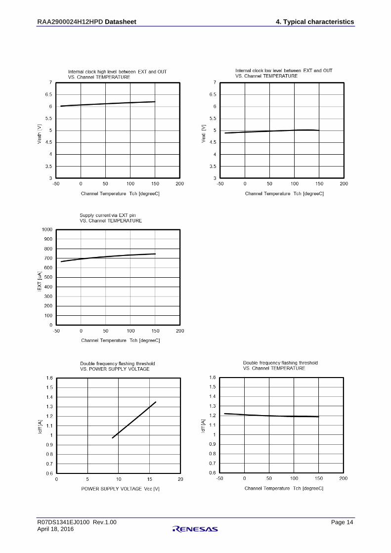
Internal clock high level between EXT and OUT
Vexth 6.10 V VCC=13.5V
Internal clock low level between EXT and OUT
Vextl 4.95 V VCC=13.5V
EXT clamp voltage Vdd,clamp 7 V IEXT=2mA, Von=0V EXT reverse clamp voltage
Vdd,rev -0.7 V IEXT=-2mA, Von=0V
Supply current via EXT pin IEXT 708 µA Von=0V, Vext=5.5V, Tch=25℃ Double frequency flashing threshold
Idff 0.85 0.96 1.06 A VCC=9V, Tch=-20 to 85℃
1.07 1.20 1.33 VCC=13.5V, Tch=-20 to 85℃
1.20 1.34 1.47 VCC=16V, Tch=-20 to 85℃ 1) not subjected production test, guaranteed by design
Protection function
Tch=-40 to 150degreeC, Vcc=9 to 16V, unless other wise specified Parameter Symbol Min Typ Max Unit Test Condition Current limitation IL(LIM) 42 A VCC=13.5V Absolute thermal shutdown temperature
aTth 150 degreeC

RAA2900024H12HPD Datasheet 3. Specification
R07DS1341EJ0100 Rev.1.00 Page 7 April 18, 2016
3.8 Feature Description
3.8.1 Normal operation When a nominal load such as defined 3.8.4 is connected to OUT pin, device operate with auto flashing mode by charging EXT capacitor up to the Vexth quickly, and then discharging EXT capacitor down to Vextl slowly with constant current IEXT.
Auto flashing operation frequency is determined following formula. Duty cycle is approx. 50%.
3.8.2 Double flashing operation at low load current condition If load current is lower than Idff during on-state, device detects low load condition, and start double flashing operation automatically.
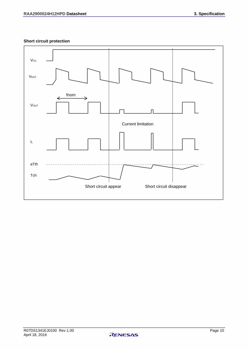
3.8.3 Short circuit protection The device shuts down automatically when Tch > aTth is detected.
Absolute thermal toggling
Current limitation control with IL(LIM) when auto restart from absolute Tch protection.
3.8.4 Nominal load Product Nominal load
RAA290002 3.4ohm
fnom = IEXT
2 × CEXT × (Vexth – Vextl)

RAA2900024H12HPD Datasheet 3. Specification
R07DS1341EJ0100 Rev.1.00 Page 8 April 18, 2016
VOUT
80%
20%
dV/dton -dV/dtoff
20%
80%
VOUT 20%
VCC
td(on)
3.8.5 Measurement condition
Switching waveform of OUT terminal
Turn on delay time after Power Supply on

RAA2900024H12HPD Datasheet 3. Specification
R07DS1341EJ0100 Rev.1.00 Page 9 April 18, 2016
3.8.6 Timing chart
Nominal Operation
Double flashing operation at low load current condition
VCC
IL
Low load current condition
Idff
VEXT
VOUT
2 x fnom fnom
VEXT
VCC
Vexth Vextl
VOUT
IL
fnom
Vextl Vexth
RAA2900024H12HPD Datasheet 3. Specification
R07DS1341EJ0100 Rev.1.00 Page 10 April 18, 2016
Short circuit protection
VCC
Tch
aTth
Short circuit appear Short circuit disappear
VEXT
VOUT
fnom
IL
Current limitation

RAA2900024H12HPD Datasheet 3. Specification
R07DS1341EJ0100 Rev.1.00 Page 11 April 18, 2016
3.9 Package drawing

RAA2900024H12HPD Datasheet 3. Specification
R07DS1341EJ0100 Rev.1.00 Page 12 April 18, 2016
3.10 Taping information
3.11 Marking information
Note: *1. Composition of the lot code
]
Week code (2 digit number)
Year code (last 1 digit number)

RAA2900024H12HPD Datasheet 4. Typical characteristics
R07DS1341EJ0100 Rev.1.00 Page 13 April 18, 2016
4. Typical characteristics
RAA2900024H12HPD Datasheet 4. Typical characteristics
R07DS1341EJ0100 Rev.1.00 Page 14 April 18, 2016

RAA2900024H12HPD Datasheet 4. Typical characteristics
R07DS1341EJ0100 Rev.1.00 Page 15 April 18, 2016

RAA2900024H12HPD Datasheet 5. Thermal characteristics
R07DS1341EJ0100 Rev.1.00 Page 16 April 18, 2016
5. Thermal characteristics

RAA2900024H12HPD Datasheet 6. Application example in principle
R07DS1341EJ0100 Rev.1.00 Page 17 April 18, 2016
6. Application example in principle
Recommended circuit for dump surge
33uF
BAT
220uF
OUT
VCC EXT
0.1uF
Vz=27V
OUT

All trademarks and registered trademarks are the property of their respective owners.
C - 1
Revision History RAA2900024H12HPD Datasheet
Rev. Date Description
Page Summary 1.00 April 18, 2016 1-17 1st issue All documents should contain the following section break and paragraph as the last item. The footers of this document refer to the paragraph in order to reference the last page of the document.
http://www.renesas.comRefer to "http://www.renesas.com/" for the latest and detailed information.
Renesas Electronics America Inc.1001 Murphy Ranch Road, Milpitas, CA 95035, U.S.A.Tel: +1-408-432-8888, Fax: +1-408-434-5351Renesas Electronics Canada Limited9251 Yonge Street, Suite 8309 Richmond Hill, Ontario Canada L4C 9T3Tel: +1-905-237-2004Renesas Electronics Europe LimitedDukes Meadow, Millboard Road, Bourne End, Buckinghamshire, SL8 5FH, U.KTel: +44-1628-651-700, Fax: +44-1628-651-804Renesas Electronics Europe GmbHArcadiastrasse 10, 40472 Düsseldorf, Germany Tel: +49-211-6503-0, Fax: +49-211-6503-1327Renesas Electronics (China) Co., Ltd.Room 1709 Quantum Plaza, No.27 ZhichunLu, Haidian District, Beijing, 100191 P. R. ChinaTel: +86-10-8235-1155, Fax: +86-10-8235-7679Renesas Electronics (Shanghai) Co., Ltd.Unit 301, Tower A, Central Towers, 555 Langao Road, Putuo District, Shanghai, 200333 P. R. China Tel: +86-21-2226-0888, Fax: +86-21-2226-0999Renesas Electronics Hong Kong LimitedUnit 1601-1611, 16/F., Tower 2, Grand Century Place, 193 Prince Edward Road West, Mongkok, Kowloon, Hong KongTel: +852-2265-6688, Fax: +852 2886-9022Renesas Electronics Taiwan Co., Ltd.13F, No. 363, Fu Shing North Road, Taipei 10543, TaiwanTel: +886-2-8175-9600, Fax: +886 2-8175-9670Renesas Electronics Singapore Pte. Ltd.80 Bendemeer Road, Unit #06-02 Hyflux Innovation Centre, Singapore 339949Tel: +65-6213-0200, Fax: +65-6213-0300Renesas Electronics Malaysia Sdn.Bhd.Unit 1207, Block B, Menara Amcorp, Amcorp Trade Centre, No. 18, Jln Persiaran Barat, 46050 Petaling Jaya, Selangor Darul Ehsan, MalaysiaTel: +60-3-7955-9390, Fax: +60-3-7955-9510Renesas Electronics India Pvt. Ltd.No.777C, 100 Feet Road, HAL 2nd Stage, Indiranagar, Bangalore 560 038, IndiaTel: +91-80-67208700, Fax: +91-80-67208777Renesas Electronics Korea Co., Ltd.17F, KAMCO Yangjae Tower, 262, Gangnam-daero, Gangnam-gu, Seoul, 06265 KoreaTel: +82-2-558-3737, Fax: +82-2-558-5338
SALES OFFICES
© 2018 Renesas Electronics Corporation. All rights reserved.Colophon 7.0
(Rev.4.0-1 November 2017)
Notice
1. Descriptions of circuits, software and other related information in this document are provided only to illustrate the operation of semiconductor products and application examples. You are fully responsible for
the incorporation or any other use of the circuits, software, and information in the design of your product or system. Renesas Electronics disclaims any and all liability for any losses and damages incurred by
you or third parties arising from the use of these circuits, software, or information.
2. Renesas Electronics hereby expressly disclaims any warranties against and liability for infringement or any other claims involving patents, copyrights, or other intellectual property rights of third parties, by or
arising from the use of Renesas Electronics products or technical information described in this document, including but not limited to, the product data, drawings, charts, programs, algorithms, and application
examples.
3. No license, express, implied or otherwise, is granted hereby under any patents, copyrights or other intellectual property rights of Renesas Electronics or others.
4. You shall not alter, modify, copy, or reverse engineer any Renesas Electronics product, whether in whole or in part. Renesas Electronics disclaims any and all liability for any losses or damages incurred by
you or third parties arising from such alteration, modification, copying or reverse engineering.
5. Renesas Electronics products are classified according to the following two quality grades: “Standard” and “High Quality”. The intended applications for each Renesas Electronics product depends on the
product’s quality grade, as indicated below.
"Standard": Computers; office equipment; communications equipment; test and measurement equipment; audio and visual equipment; home electronic appliances; machine tools; personal electronic
equipment; industrial robots; etc.
"High Quality": Transportation equipment (automobiles, trains, ships, etc.); traffic control (traffic lights); large-scale communication equipment; key financial terminal systems; safety control equipment; etc.
Unless expressly designated as a high reliability product or a product for harsh environments in a Renesas Electronics data sheet or other Renesas Electronics document, Renesas Electronics products are
not intended or authorized for use in products or systems that may pose a direct threat to human life or bodily injury (artificial life support devices or systems; surgical implantations; etc.), or may cause
serious property damage (space system; undersea repeaters; nuclear power control systems; aircraft control systems; key plant systems; military equipment; etc.). Renesas Electronics disclaims any and all
liability for any damages or losses incurred by you or any third parties arising from the use of any Renesas Electronics product that is inconsistent with any Renesas Electronics data sheet, user’s manual or
other Renesas Electronics document.
6. When using Renesas Electronics products, refer to the latest product information (data sheets, user’s manuals, application notes, “General Notes for Handling and Using Semiconductor Devices” in the
reliability handbook, etc.), and ensure that usage conditions are within the ranges specified by Renesas Electronics with respect to maximum ratings, operating power supply voltage range, heat dissipation
characteristics, installation, etc. Renesas Electronics disclaims any and all liability for any malfunctions, failure or accident arising out of the use of Renesas Electronics products outside of such specified
ranges.
7. Although Renesas Electronics endeavors to improve the quality and reliability of Renesas Electronics products, semiconductor products have specific characteristics, such as the occurrence of failure at a
certain rate and malfunctions under certain use conditions. Unless designated as a high reliability product or a product for harsh environments in a Renesas Electronics data sheet or other Renesas
Electronics document, Renesas Electronics products are not subject to radiation resistance design. You are responsible for implementing safety measures to guard against the possibility of bodily injury, injury
or damage caused by fire, and/or danger to the public in the event of a failure or malfunction of Renesas Electronics products, such as safety design for hardware and software, including but not limited to
redundancy, fire control and malfunction prevention, appropriate treatment for aging degradation or any other appropriate measures. Because the evaluation of microcomputer software alone is very difficult
and impractical, you are responsible for evaluating the safety of the final products or systems manufactured by you.
8. Please contact a Renesas Electronics sales office for details as to environmental matters such as the environmental compatibility of each Renesas Electronics product. You are responsible for carefully and
sufficiently investigating applicable laws and regulations that regulate the inclusion or use of controlled substances, including without limitation, the EU RoHS Directive, and using Renesas Electronics
products in compliance with all these applicable laws and regulations. Renesas Electronics disclaims any and all liability for damages or losses occurring as a result of your noncompliance with applicable
laws and regulations.
9. Renesas Electronics products and technologies shall not be used for or incorporated into any products or systems whose manufacture, use, or sale is prohibited under any applicable domestic or foreign laws
or regulations. You shall comply with any applicable export control laws and regulations promulgated and administered by the governments of any countries asserting jurisdiction over the parties or
transactions.
10. It is the responsibility of the buyer or distributor of Renesas Electronics products, or any other party who distributes, disposes of, or otherwise sells or transfers the product to a third party, to notify such third
party in advance of the contents and conditions set forth in this document.
11. This document shall not be reprinted, reproduced or duplicated in any form, in whole or in part, without prior written consent of Renesas Electronics.
12. Please contact a Renesas Electronics sales office if you have any questions regarding the information contained in this document or Renesas Electronics products.
(Note 1) “Renesas Electronics” as used in this document means Renesas Electronics Corporation and also includes its directly or indirectly controlled subsidiaries.
(Note 2) “Renesas Electronics product(s)” means any product developed or manufactured by or for Renesas Electronics.