intel premiere pci motherboard manual 1994
DESCRIPTION
Manual for Intel Premiere PCI Socket motherboard supporting Pentium 60 and 66 MHz processors. Enjoy!TRANSCRIPT

Premiere/PCIBaby-AT Board & Expandable DesktopTechnical Product Summary
Final Review Copy Version 2.0
March, 1994
Order Number 281604-002

Premiere/PCI Baby-AT Technical Product Summary • Page 2
®

Classic/PCI Baby-AT Technical Product Summary • Page 3
Intel Corporation disclaims all warranties and liabilities for the use of this document and the information contained herein, and assumes noresponsibility for any errors which may appear in this document. Intel makes no commitment to update the information contained herein, andmay make changes at any time without notice. There are no express or implied licenses granted hereunder to any intellectual property rights ofIntel Corporation or others to design or fabricate Intel integrated circuits or integrated circuits based on the information in this document.
Contact your local sales office to obtain the latest specifications before placing your order.
The following are trademarks of Intel Corporation and may only be used to identify Intel products:AboveActionMediaDVIEtherExpressExCAFlashFilei287i386i387i486i487i750i860i960
ICEiCOMPIndeoInsight960™Intel287Intel386Intel387Intel486Intel487Intel InsideIntelDX2™IntelDX4™iPSCiRMX®
LANDeskMCSNetPortNetportExpress™OverDriveParagonPentiumRapdiCADSatisFAXtionSolutions960™StorageExpressTokenExpress
The Indeo, OverDrive and Pentium logos are trademarks and the Intel and Intel Inside logos are registered trademarks of Intel Corporation.
Intel Corporation and Intel’s FASTPATH are not affiliated with Kinetics, a division of Excelan, Inc. or its FASTPATH trademark or products.
MDS is an ordering code only and is not used as a product name or trademark. MDS is a trademark or registered trademark of its respectiveowner.
Additional copies of Intel literature may be obtained from:
Intel CorporationLiterature SalesP.O. Box 7641Mt. Prospect, IL 60056-7641
TRADEMARK ACKNOWLEDGMENTS
Centronics is a trademark of Centronics Data Computer Corp.IBM, MDA, MCGA, EGA, VGA, Personal System/2, PS/2, PC/XT and PC/AT are trademarks of International Business Machines.PolySwitch is a registered trademark of Raychem Corporation.
All other brands and names are the property of their respective owners.
INTEL CORPORATION, 1994281604-002
Premiere/PCI Baby-AT Technical Product Summary • Page 4
Premiere/PCI Baby-AT Motherboard & Expandable DesktopTechnical Product Summary
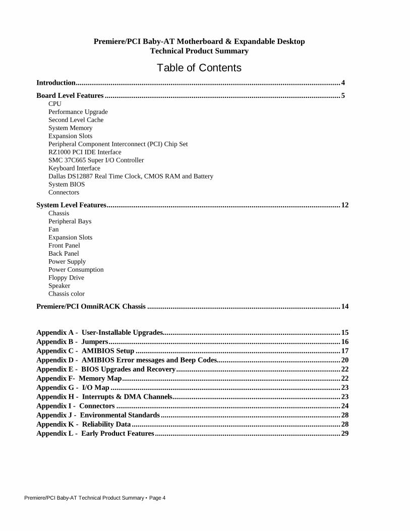
Table of ContentsIntroduction.........................................................................................................................................4
Board Level Features ..........................................................................................................................5CPUPerformance UpgradeSecond Level CacheSystem MemoryExpansion SlotsPeripheral Component Interconnect (PCI) Chip SetRZ1000 PCI IDE InterfaceSMC 37C665 Super I/O ControllerKeyboard InterfaceDallas DS12887 Real Time Clock, CMOS RAM and BatterySystem BIOSConnectors
System Level Features.........................................................................................................................12ChassisPeripheral BaysFanExpansion SlotsFront PanelBack PanelPower SupplyPower ConsumptionFloppy DriveSpeakerChassis color
Premiere/PCI OmniRACK Chassis ....................................................................................................14
Appendix A − User-Installable Upgrades............................................................................................15Appendix B − Jumpers........................................................................................................................16Appendix C − AMIBIOS Setup ..........................................................................................................17Appendix D − AMIBIOS Error messages and Beep Codes................................................................20Appendix E − BIOS Upgrades and Recovery.....................................................................................22Appendix F− Memory Map.................................................................................................................22Appendix G − I/O Map .......................................................................................................................23Appendix H − Interrupts & DMA Channels.......................................................................................23Appendix I − Connectors ....................................................................................................................24Appendix J − Environmental Standards .............................................................................................28Appendix K − Reliability Data ............................................................................................................28Appendix L − Early Product Features ................................................................................................29

Premiere/PCI Baby-AT Technical Product Summary • Page 5
IntroductionThe Premiere/PCI Expandable Desktop is a state-of-the-art platform delivering the latest Pentiummicroprocessor and I/O technology on an industry-standard Baby-AT form factor motherboard. It is ideal fordemanding desktop applications requiring the maximum in I/O expansion flexibility.
A 60 MHz or 66 MHz Pentium microprocessor is complemented by a 256 KB second level write-back cacheto provide workstation- level computing performance. A Pentium OverDrive socket provides access tofuture performance enhancements, and SIMM sockets support up to 128 MB of system memory.
The Premiere/PCI Baby-AT motherboard offers outstanding I/O capabilities. Three PCI local bus slotsprovide a high bandwidth data path for data-intensive functions such as graphics and disk I/O. Integratedperipherals include the RZ1000, which provides a PCI local bus primary IDE interface, as well as the SMC37C665 Super I/O component, which provides floppy and secondary IDE drive interfaces, two FIFO serialports and an ECP-capable parallel port. Five ISA slots complete the I/O mix.
STANDARD BABY-AT FORM FACTOR
The Premiere/PCI Baby-AT motherboard conforms to the industry standard Baby-AT form factor. It meetsthe specifications for maximum board size, board mounting locations, expansion slot placement, andkeyboard connector location. In addition to complying to the standard, the Premiere/PCI Baby-AT providesthree slots which will accommodate PCI expansion cards.
8.6"
0.3"
6.6"
12.6"
13.0"
5.6"0.5"
0.5"
5.6"
Figure 1. Premiere/PCI Baby-AT Motherboard dimensions.

Premiere/PCI Baby-AT Technical Product Summary • Page 6
Board Level Features
A. Power supply connectorsB. Super I/O controllerC. Flash EEPROM containing the BIOSD. Real-time clock, CMOS RAM, and integral batteryE. Floppy diskette drive connectorF. IDE Connector on ISA busG. Angled (low profile) SIMM connectorsH. Vertical SIMM connectorI. Pentium microprocessorJ. Mercury chip setK. Auxiliary (3.3 v) PCI power connectorL. Parallel connectorM. COM2 (RS232) connectorN. COM1 (RS232) connectorO. Keyboard connectorP. IDE Connector on PCI local bus
Figure 2. Premiere/PCI Baby-AT Motherboard components
CPU
The Premiere/PCI Baby-AT motherboard is designed to operate with either a 60 MHz or 66 MHz Pentiummicroprocessor. This processor is compatible with the 8086, 80286, i386 and i486 CPUs. It supportsboth read and write burst mode bus cycles, and includes an on-chip 16 KB cache which is split into 8 KBcode and 8 KB data caches employing a write-back policy. The Pentium processor also integrates anadvanced numeric coprocessor which significantly increases the speed of floating point operations, whilemaintaining compatibility with i486 DX math coprocessors and complying with ANSI/IEEE standard754-1985.
Premiere/PCI Baby-AT motherboards equipped with 66 MHz Pentium processors have a voltage controlcircuit that regulates Vcc to the CPU and frequency synthesizer. The voltage regulation accomodates avariety of Intel CPUs and increases the overall robustness and reliability of the motherboard. Boardswithout the voltage regulator circuitry cannot reliably use 66 MHz Pentium processors.
The motherboard contains two mounting holes which allow a dedicated fan to be located directly in front ofthe CPU socket. A 12 volt connector suitable for a CPU fan is located close to the mounting holes.
PERFORMANCE UPGRADE
A 273-pin Type 4 Zero Insertion Force socket provides users with a performance upgrade path usingPentium OverDrive processors. The OverDrive processor being developed for use in this socket willprovide performance beyond that delivered by the Pentium microprocessor.
SECOND LEVEL CACHE
The Pentium processor's internal cache is complemented with a 256 KB direct mapped, write-thru secondlevel cache implemented with eight 32Kx8, 15 ns SRAM devices. Tag and control logic is contained in the82434LX PCMC core chip.
Premiere/PCI Baby-AT Technical Product Summary • Page 7
SYSTEM MEMORY
The Premiere/PCI motherboard provides four 72-pin SIMM sites for memory expansion. The socketssupport 256K x 36 (1 MB), 512K x 36 (2 MB), 1M x 36 (4 MB), 2M x 36 (8 MB), 4M x 36 (16 MB),and 8M x 36 (32 MB) SIMM modules. Minimum memory size is 2 MB and maximum memory size, usingfour 8M x 36 SIMM modules, is 128 MB. Memory timing requires 70 ns fast page devices. Paritygeneration/checking is provided for each byte. Non-parity 32 bit SIMMs also may be used, in which casethe parity generation/checking circuitry is automatically disabled.
The four sockets are arranged as Bank A and Bank B, with each bank consisting of two sockets andproviding a 64-bit wide data path and 8 parity bits. Both SIMMs in a bank must be of the same memorysize and type, although Banks A and B may have different types of memory installed. Bank A only, Bank Bonly, or both banks may be populated. There are no jumper settings required for the memory size, which isautomatically detected by the system BIOS. Tin-lead SIMMs should be used when adding DRAM.
The memory array is controlled by the Intel 82434LX PCMC and data buffering is provided by two Intel82433LX Local Bus Extension devices.
EXPANSION SLOTS
Up to seven expansion slots may be populated on the Premiere/PCI Baby-AT motherboard. Expansioncards are oriented perpendicular to the motherboard.
There are five ISA bus expansion connectors and three PCI expansion connectors. One slot is shared byconnectors that will accommodate either an ISA or a PCI expansion card, but not both at the same time. Allthree PCI expansion slots accept PCI master cards to fully support the PCI specification.
The motherboard design limits the length of add-in cards in some slots. The height of the CPU heat sinklimits the use of the two PCI connectors at J10C1 and J10C2 to less than full-length devices. The length ofcards installed in the ISA connector at J10F1 may be limited if a SIMM is installed in the vertical SIMMsocket (J3F1). And the location of the serial port header may limit the type of card that can be installed inthe ISA connector at J10G1.
PCI 3.3 VOLT CAPABILITIES
To maintain strict compliance with the PCI specification, the motherboard provides a connector whichcan be used to route 3.3 volt power to the PCI slots. The connector may be used with a separate 3.3 voltpower supply or with a custom designed voltage converter.
PERIPHERAL COMPONENT INTERCONNECT (PCI) CHIP SET
The Intel Mercury chip set consists of one 82434LX PCI/Cache/Memory Controller (PCMC), two82433LX Local Bus eXtension (LBX) devices, and one 82378IB System I/O (SIO) bridge chip. TheMercury chip set provides the following functions:
• CPU reset control• CPU L1 cache control• CPU burst mode control• CPU interface control• Integrated second level write-back cache
controller with tag comparator•Fast Page-mode DRAM controller• Burst memory read/write control logic• Data bus conversion to PCI• Parity generation/detection to memory
• AT-BUS direction control• Chip select for keyboard controller and RTC• Speaker control• NMI logic• Floating-point coprocessor interface• Keyboard reset, gate A20 emulation logic• DMA controller• Interrupt controller• Counters/Timers

Premiere/PCI Baby-AT Technical Product Summary • Page 8
82434LX PCI/CACHE/MEMORY CONTROLLER (PCMC)
The 82434LX provides all control signals necessary to drive a second level cache and the DRAM array,including multiplexed address signals. It also controls system access to memory and generates snoopcontrols to maintain cache coherency.
82433LX LOCAL BUS EXTENSION (LBX)
There are two 82433LX components which provide data bus buffering and dual port buffering to thememory array. Controlled by the 82434LX, the 82433LX devices add one load each to the PCI bus andperform all the necessary byte and word swapping. The devices include memory and I/O write buffers.
82378IB SYSTEM I/O (SIO)
The 82378IB integrates seven 32-bit DMA channels, five 16-bit timer/counters, two eight-channelinterrupt controllers, NMI logic, ISA refresh address generation, and PCI/ISA bus arbitration circuitrytogether onto the same device.
Detailed information on the chip set is available in the Intel 82430 PCISet data sheet.
RZ1000 PCI IDE INTERFACE
The Premiere/PCI Baby-AT motherboard offers two IDE channels: one on the PCI local bus and one on theISA bus. PCI-based IDE provides performance much improved over the traditional ISA-based IDE.
PCI TO IDE INTERFACE CIRCUIT
An onboard PCI to IDE interface is provided by the PCTech RZ1000 component and a specially-tunedsystem BIOS, which is fully compatible with existing IDE software. The RZ1000 provides a 32-bitbuffered interface to two IDE drives, allowing these drives to be accessed at full PCI bandwidth. Thecomponent also supports Enhanced IDE Mode 3 timing, allowing the drive to transfer data at its fullbandwidth. The system BIOS provides transparent access to these features, as well as support forLogical Block Addressing (LBA) which allows the use of drives larger than 528 MB. The PCI IDEinterface functions as the primary interface using Interrupt 14. A sdecondary IDE interface (IRQ15) isprovided by the SMC 37C665 I/O controller.
IDE PHYSICAL INTERFACE
The PCI IDE physical interface consists of a dedicated 40-pin header connector (J11F1). A separate 40-pin connector is dedicated to the SMC 37C655 IDE interface. When the on-board IDE controllers areenabled, the RZ1000 is the primary interface and the ISA IDE controller is the secondary interface.
SMC 37C665 SUPER I/O CONTROLLER
Control for the integrated serial ports, parallel port, floppy drive and IDE hard drive interface isincorporated into a single component, the SMC FDC37C665. This component provides:
•Two NS16C552-compatible UARTs with send/receive 16 byte FIFO•Multi-mode bi-directional parallel port
- Standard mode; IBM* and Centronics compatible- Enhanced Parallel Port (EPP) with BIOS/Driver support- High Speed mode; Extended Capabilities Port (ECP) compatible
•Industry standard floppy controller with 16 byte data FIFO (2.88 MB floppy support)•IDE hard disk decode and chip select
Header pins located near the back of the board allow cabling to use these interfaces. The serial ports can beenabled as COM1 and COM2, or disabled. The parallel port can be configured via the Setup program asLPT1 or disabled, and can be set as bi-directional or output only when enabled. The IDE interface supportsstandard, Type B, and Type F DMA.
Premiere/PCI Baby-AT Technical Product Summary • Page 9
KEYBOARD INTERFACE
An Intel 8742 surface mount microcontroller contains the Phoenix Technologies-compatiblekeyboard/mouse controller code. An AT-style keyboard connector is located on the back panel side of themotherboard. The 5V line on this connector is protected with a PolySwitch* circuit which acts much like aself-healing fuse, re-establishing the connection after an over-current condition is removed. While thisdevice eliminates the possibility of having to replace a fuse, care should be taken to turn off the systempower before installing or removing a keyboard.
The 8742 microcontroller code supports Power-On/Reset (POR) password protection. The POR passwordis set via the Setup program. The keyboard controller also provides for the following "hot key" sequences:
•CTRL-ALT-DEL: System software reset. This sequence performs a software reset of the systemby jumping to the beginning of the BIOS code and running the POST operation.
•CTRL-ALT+ and CTRL-ALT-: Turbo mode selection. CTRL-ALT- sets the system for de-turbo mode (emulation of an 8 MHz 80286 CPU) and CTRL-ALT+ sets the system for turbomode (normal operation at 60 MHz). Changing the Turbo mode may be prohibited by anoperating system or application software. For example, the CPU speed cannot be changed withthe hot keys when the CPU is in Protected Mode.
DALLAS DS12887 REAL TIME CLOCK, CMOS RAM AND BATTERY
The Real Time Clock (RTC) is implemented using a Dallas DS12887 device. The DS12887 is accurate towithin 13 minutes/year and requires no external support (the battery and oscillator are integrated into thedevice). The internal battery has an estimated lifetime of ten years.
The RTC can be set via the BIOS SETUP Program. CMOS memory supports the standard 128-bytebattery-backed RAM, fourteen bytes for clock and control registers, and 114 bytes of general purpose non-volatile CMOS RAM. All CMOS RAM is reserved for BIOS use. The CMOS RAM can be set to specificvalues or cleared to the system default values using the BIOS SETUP program. Also, the CMOS RAMvalues can be cleared to the system defaults by using a hardware jumper. Appendix B lists jumperconfigurations.
SYSTEM BIOS
The Premiere/PCI Baby-AT motherboard uses an American Megatrends Incorporated (AMI) ROM BIOS,which is stored in Flash EEPROM and easily upgraded using a floppy disk-based program. BIOS upgradeswill be available for download from the Intel bulletin board system. In addition to the AMIBIOS, the FlashEEPROM also contains the Setup utility, Power-On Self Tests (POST), update recovery code, and the PCIauto-configuration utility. This motherboard supports system BIOS shadowing, allowing the BIOS toexecute from 32-bit on-board write-protected DRAM.
The BIOS displays a sign-on message during POST identifying the type of BIOS and a five-digit revisioncode. First production units will display a revision code of 1.00.01.AF2 As BIOS updates occur, therevision number will increase to 1.00.02.AF2, and so on.
Information on BIOS functions can be found in the IBM PS/2 and Personal Computer BIOS TechnicalReference published by IBM, and the ISA and EISA Hi-Flex AMIBIOS Technical Reference published byAMI. Both manuals are available at most technical bookstores.
Premiere/PCI Baby-AT Technical Product Summary • Page 10
FLASH IMPLEMENTATION
The Intel 28F001BXT 1 Mb FLASH component is organized as 128K x 8 (128 KB). The Flash device isdivided into five areas, as described in Table 1.
System Address FLASH Memory AreaF0000H FFFFFH 64 KB Main BIOSEE000H EFFFFH 8 KB Boot Block (Not FLASH erasable)ED000H EDFFFH 4 KB OEM LOGO AreaE8000H ECFFFH 20 KB System BIOS ReservedE0000H E7FFFH 32 KB Not Used
Table 1. Flash Memory Organization
The FLASH device resides in system memory in two 64 KB segments starting at E0000H, and can bemapped two different ways, depending on the mode of operation. In Normal Mode, address line A16 isinverted, setting the E000H and F000H segments so that the BIOS is organized as shown in the systemaddress column above. Recovery mode removes the inversion on address line A16, swapping the E000Hand F000H segments so that the 8 KB boot block resides at FE000H where the CPU expects thebootstrap loader to exist. This mode is only necessary in the unlikely event that a BIOS upgradeprocedure is interrupted, causing the BIOS area to be left in an unusable state. For information onrecovering the BIOS in the event of a catastrophic failure, refer to Appendix E.
BIOS UPGRADES
Flash memory makes distributing BIOS upgrades easy. A new version of the BIOS can be installed froma diskette. BIOS upgrades will be available for download from the bulletin board system.
The disk-based Flash upgrade utility (FMUP.EXE) has three options for BIOS upgrades:
• The Flash BIOS can be updated from a file on a disk;
• The current BIOS code can be copied from the Flash EEPROM to a disk file as a backup inthe event that an upgrade cannot be successfully completed; or
• The BIOS in the Flash device can be compared with a disk file to ensure the system has thecorrect BIOS version.
The upgrade utility ensures the upgrade BIOS matches the target system to prevent accidentally installinga BIOS for a different type of system. Security to prevent unauthorized changes to the BIOS is providedvia a write-protect jumper. The default setting is to allow BIOS upgrades. A recovery jumper is providedto allow recovery in the unlikely event of an unsuccessful BIOS upgrade. The jumper forces the ROMdecode to access an 8 KB block of write protected recovery code in the Flash device.
SETUP UTILITY
The ROM-based Setup utility allows the configuration to be modified without opening the system formost basic changes. The Premiere/PCI Baby-AT motherboard also incorporates many new capabilitiesinto the Flash EEPROM, including:
•Auto configuration of IDE hard disks (manual selection of the drive type is no longer required).
•Support for two IDE disk interfaces (primary and secondary) providing access to 4 IDEdevices (when a second IDE controller is added on the PCI or ISA bus).
•An option allowing the user to assign a block of addresses below the 1 MB boundary as non-shadowed, non-cached. This area is primarily used for expansion card ROM which causestiming problems when shadowed and cached.
•ISA interrupts IRQ9, IRQ10 and IRQ11 may be assigned to add-in card ISA adapters, therebyinforming the PCI configuration utility which interrupts not to use.
Premiere/PCI Baby-AT Technical Product Summary • Page 11
The Setup utility is accessible only during the Power-On Self Test (POST) by pressing the <DEL> or<F1> key after the POST memory test has begun and before boot begins. A prompt may be enabled thatinforms users to press the <F1> key to access Setup. A motherboard jumper can be set to prevent useraccess to Setup for security purposes. Setup options are detailed in Appendix C.
PCI AUTO-CONFIGURATION CAPABILITY
The PCI auto-configuration utility operates in conjunction with the system Setup utility to allow theinsertion and removal of PCI cards to the system without user intervention. When the system is turned onafter adding a PCI add-in card, the BIOS automatically configures interrupts, I/O space, and otherparameters. The user does not have to configure jumpers or worry about potential resource conflicts.Because PCI cards use the same interrupt resources as ISA cards, the user must specify the interruptsused by ISA add-in cards in the Setup utility. The PCI Auto-Configuration function complies withversion 2.0G of the PCI BIOS specification.
SECURITY FEATURES
BIOS Password
A BIOS password feature provides security during the boot process. A password can be enteredusing the Setup utility and must be re-entered prior to disk boot each time the system is reset. Toenable, disable, or change the password, refer to the Setup program options in Appendix C.
If the password is forgotten, it can be cleared by turning off the system and setting the "passwordclear" jumper to the clear position.
Setup Enable Jumper
A baseboard jumper controls access to the BIOS Setup utility. By setting jumper to the disableposition, the user is prevented from accessing the Setup utility at any time.
CONNECTORS
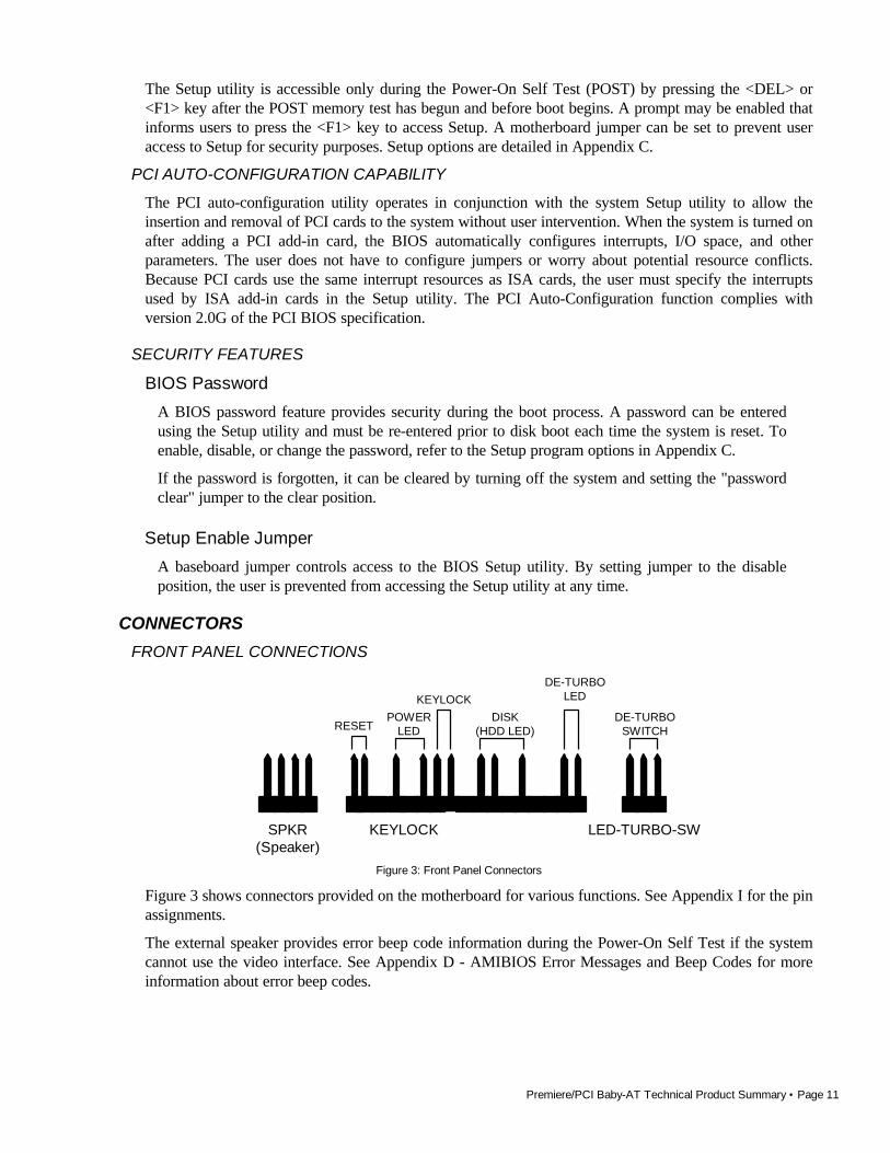
FRONT PANEL CONNECTIONS
KEYLOCK LED-TURBO-SWSPKR(Speaker)
RESETPOWER
LED
KEYLOCKDISK
(HDD LED)
DE-TURBOLED
DE-TURBOSWITCH
Figure 3: Front Panel Connectors
Figure 3 shows connectors provided on the motherboard for various functions. See Appendix I for the pinassignments.
The external speaker provides error beep code information during the Power-On Self Test if the systemcannot use the video interface. See Appendix D - AMIBIOS Error Messages and Beep Codes for moreinformation about error beep codes.

Premiere/PCI Baby-AT Technical Product Summary • Page 12
BACK PANEL CONNECTIONS
The Premiere/PCI Baby-AT includes an AT-style keyboard connector integrated on the back panel sideof the motherboard.
I/O CONNECTIONS
The motherboard contains stake pin header connections for cabling the serial, parallel, floppy, and IDEinterfaces. Figure 4 shows the locations of these connectors, orientation of pin 1 on each, the numberingof each connector, and for IDE and Floppy, the missing key pin.
Fast Fan is the default connection and provides 12V power for operating the fan. For slower and quieterfan operation (less cooling), the Slow Fan connector provides 10V power.
Figure 4. I/O Connections

Premiere/PCI Baby-AT Technical Product Summary • Page 13
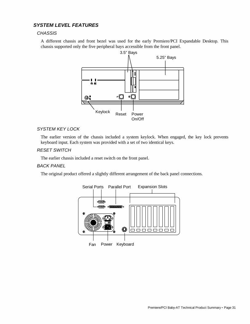
System Level Features
CHASSIS
The Premiere/PCI Expandable Desktop easily provides the expandability required for most traditional PCapplications − seven peripheral bays, seven expansion slots, an ample 200 watt power supply and anadditional fan located at the front left side of the chassis to help keep the system cool. The user can accessfive of the peripheral bays from the front of the chassis. The Premiere/PCI Expandable Desktop also meetsstringent environmental requirements.
PERIPHERAL BAYS3.5” Bays 5.25” Bays Power
Figure 5: Premiere/PCI Expandable Desktop Front Panel
Seven expansion bays are available for peripherals and other add-in devices. These include three 5¼" half-height bays and two 3½" one-inch bays that are accessible from the front panel. Two internal 3½"peripheral bays are located above the power supply.
FAN
The Premiere/PCI Expandable Desktop has two fans to keep the system cool. One fan within the powersupply provides 28 cfm of air movement. The second fan, located behind the card guide, provides 26 cfmacross the add-in cards and the CPU. The second fan receives 12 Vdc directly from the baseboard at stakepin location J1D1.
EXPANSION SLOTS
The Premiere/PCI Expandable Desktop has seven expansion card slots, as shown in Figure 6. Several ofthe slots are intended for use with less than full-length cards. One ISA slot is limited in length by the 3½"peripheral bay carrier, one ISA card slot is limited in length by the left-most SIMM socket, two ISA cardslots are full length, two PCI slots are limited in length by the CPU heatsink, and one is a full length sharedslot, accepting either an ISA or a PCI expansion card.
FRONT PANEL
The Premiere/PCI Expandable Desktop front panel consists of a power switch, a power-on LED and a harddisk access LED. Five peripheral bays also can be accessed from the front panel, as shown in Figure 5.
BACK PANEL
The back panel consists of access panels for the expansion slots (one location is unused), two DB9 RS-232serial ports, a bi-directional parallel port, an AT-style keyboard connector, a 115/230 voltage switch, apower supply input, an auxiliary power output and the power supply fan. Punch-out locations also areprovided for adding a second parallel port and a SCSI-2 connector.

Premiere/PCI Baby-AT Technical Product Summary • Page 14
Fan Power Keybd Expansion Slots
Serial PortsParallel Port ISA PCI ComboUnused
Figure 6. Premiere/PCI Expandable Desktop Back Panel.
POWER SUPPLY
The Premiere/PCI Expandable Desktop integrates a 200 watt switchable power supply for all onboardresources, add-in cards, and peripherals. The Astec Corp. model SA201-3440 supports operating settingsat 100-120 VAC (5 Amps AC) or 200-240 VAC (3 Amps AC). The input voltage is selected using aswitch on the back of the system.
AC POWER INPUT SPECIFICATIONS
Input frequency 50/60 HzAC Voltage Current
90-135 5.0 A180-265 3.0 ATable 2. Power Supply Input Specifications.
DC OUTPUT SPECIFICATIONS
DC Voltage Max. Continuous Current Peak Current 15 Seconds Minimum Current Load+5V 22.0A - 3.0A-5V 0.5A - 0A
+12V 8.0A 9.0 A 0A-12V 0.5A - 0A
Table 3. Power Supply DC Output Specifications.
POWER CONSUMPTION
Table 4 lists the current used by system resources in a configuration which includes 8 MB of DRAM.Table 5 lists the typical power consumed by the same configuration. This information is preliminary and isprovided only as a guide for calculating approximate total system power usage with additional resourcesadded.
CURRENTDC Voltage Max. Continuous Current Peak Current 15 Seconds Minimum Current Load
+5V 18.5A 18.5 2.5A-5V 0.9A 0.9A 0A
+12V 4.6A 9.5A 0.5A-12V 0.5A 0.5A 0A
Table 4. Premiere/PCI Expandable Desktop Current Requirements (Preliminary)
WATTSResource Typical PowerPremiere/PCI Expandable Desktop baseboard, 8 MB , 256 KB cache 50 wattsTeac 3½" Floppy drive 1.7 watts
Table 5. Current Use by System Resources (Preliminary)

Premiere/PCI Baby-AT Technical Product Summary • Page 15
FLOPPY DRIVE
The Premiere/PCI Expandable Desktop integrates a 3½" Teac Floppy drive Model FD-235HF into theright 3½" bay. This is the same proven floppy disk drive that has been used on many previous Intelsystems.
SPEAKER
The standard system ships with an external speaker installed. The user may enable/disable the device usingthe Setup utility or program the speaker via port 61H. The speaker provides error beep code informationduring POST if the system cannot use the video interface. The Premierec/PCI Expandable Desktop productguide (order # 616545) contains detailed beep and error code information.
CHASSIS COLOR
The chassis color is beige. The bottom and back of the chassis are not painted.
Premiere/PCI OmniRACK ChassisThe Premiere/PCI Baby-AT motherboard also is available in Intel's OmniRACK rackmountable chassis.OmniRACK can be used in an industry-standard REA 19-inch equipment rack or as an embeddedmicrocomputer. Premiere/PCI OmniRACK offers a 230 watt power supply with temperature-controlledinternal cooling fans. The system contains four peripheral bays (two 5¼" x 1.6", one 3½" x 1.6", and one3½" x 1") housed in a removable drive cage. For more information on the OmniRack chassis, see theOmniRACK Technical Product Summary, available from Intel Literature or the bulletin board system.
The order code for the Premiere/PCI OmniRACK product is ORP605P8.
Figure 7. OmniRACK Chassis with access door closed
Premiere/PCI Baby-AT Technical Product Summary • Page 16
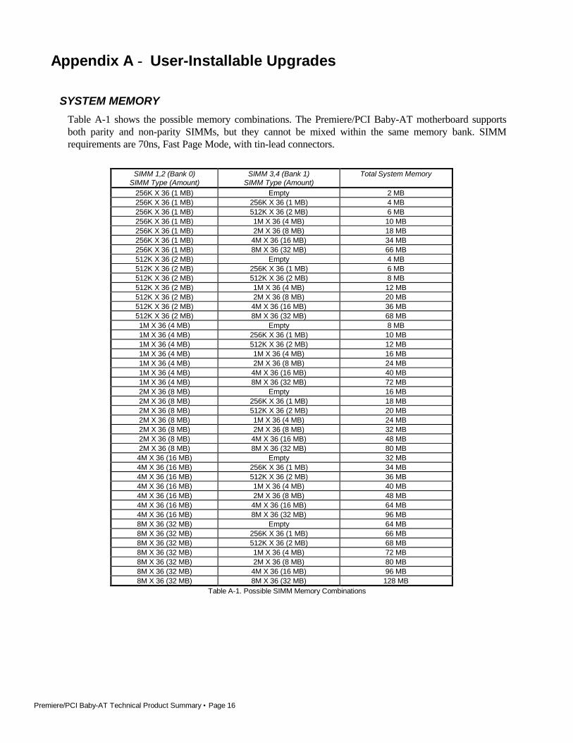
Appendix A − User-Installable Upgrades
SYSTEM MEMORY
Table A-1 shows the possible memory combinations. The Premiere/PCI Baby-AT motherboard supportsboth parity and non-parity SIMMs, but they cannot be mixed within the same memory bank. SIMMrequirements are 70ns, Fast Page Mode, with tin-lead connectors.
SIMM 1,2 (Bank 0)SIMM Type (Amount)
SIMM 3,4 (Bank 1)SIMM Type (Amount)
Total System Memory
256K X 36 (1 MB) Empty 2 MB256K X 36 (1 MB) 256K X 36 (1 MB) 4 MB256K X 36 (1 MB) 512K X 36 (2 MB) 6 MB256K X 36 (1 MB) 1M X 36 (4 MB) 10 MB256K X 36 (1 MB) 2M X 36 (8 MB) 18 MB256K X 36 (1 MB) 4M X 36 (16 MB) 34 MB256K X 36 (1 MB) 8M X 36 (32 MB) 66 MB512K X 36 (2 MB) Empty 4 MB512K X 36 (2 MB) 256K X 36 (1 MB) 6 MB512K X 36 (2 MB) 512K X 36 (2 MB) 8 MB512K X 36 (2 MB) 1M X 36 (4 MB) 12 MB512K X 36 (2 MB) 2M X 36 (8 MB) 20 MB512K X 36 (2 MB) 4M X 36 (16 MB) 36 MB512K X 36 (2 MB) 8M X 36 (32 MB) 68 MB1M X 36 (4 MB) Empty 8 MB1M X 36 (4 MB) 256K X 36 (1 MB) 10 MB1M X 36 (4 MB) 512K X 36 (2 MB) 12 MB1M X 36 (4 MB) 1M X 36 (4 MB) 16 MB1M X 36 (4 MB) 2M X 36 (8 MB) 24 MB1M X 36 (4 MB) 4M X 36 (16 MB) 40 MB1M X 36 (4 MB) 8M X 36 (32 MB) 72 MB2M X 36 (8 MB) Empty 16 MB2M X 36 (8 MB) 256K X 36 (1 MB) 18 MB2M X 36 (8 MB) 512K X 36 (2 MB) 20 MB2M X 36 (8 MB) 1M X 36 (4 MB) 24 MB2M X 36 (8 MB) 2M X 36 (8 MB) 32 MB2M X 36 (8 MB) 4M X 36 (16 MB) 48 MB2M X 36 (8 MB) 8M X 36 (32 MB) 80 MB
4M X 36 (16 MB) Empty 32 MB4M X 36 (16 MB) 256K X 36 (1 MB) 34 MB4M X 36 (16 MB) 512K X 36 (2 MB) 36 MB4M X 36 (16 MB) 1M X 36 (4 MB) 40 MB4M X 36 (16 MB) 2M X 36 (8 MB) 48 MB4M X 36 (16 MB) 4M X 36 (16 MB) 64 MB4M X 36 (16 MB) 8M X 36 (32 MB) 96 MB8M X 36 (32 MB) Empty 64 MB8M X 36 (32 MB) 256K X 36 (1 MB) 66 MB8M X 36 (32 MB) 512K X 36 (2 MB) 68 MB8M X 36 (32 MB) 1M X 36 (4 MB) 72 MB8M X 36 (32 MB) 2M X 36 (8 MB) 80 MB8M X 36 (32 MB) 4M X 36 (16 MB) 96 MB8M X 36 (32 MB) 8M X 36 (32 MB) 128 MB
Table A-1. Possible SIMM Memory Combinations
Premiere/PCI Baby-AT Technical Product Summary • Page 17
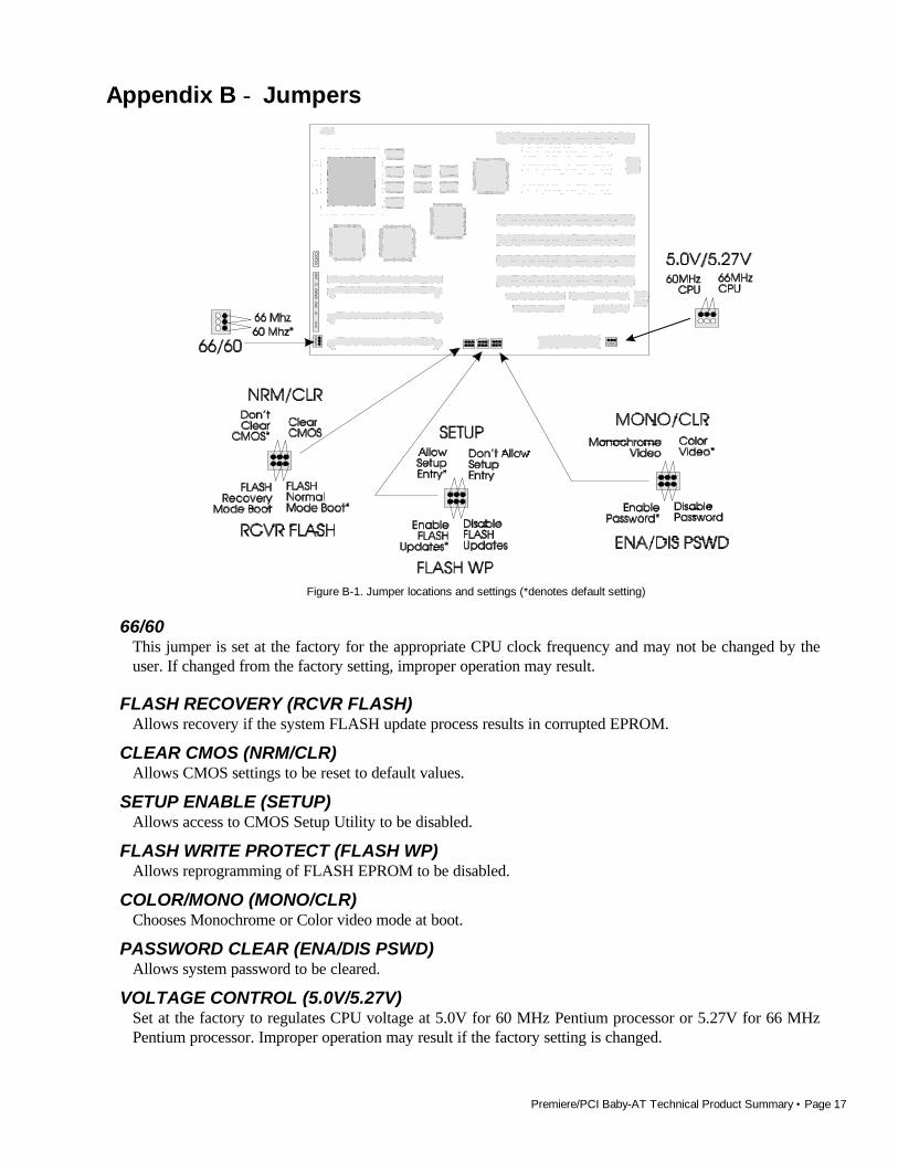
Appendix B − Jumpers
Figure B-1. Jumper locations and settings (*denotes default setting)
66/60This jumper is set at the factory for the appropriate CPU clock frequency and may not be changed by theuser. If changed from the factory setting, improper operation may result.
FLASH RECOVERY (RCVR FLASH)Allows recovery if the system FLASH update process results in corrupted EPROM.
CLEAR CMOS (NRM/CLR)Allows CMOS settings to be reset to default values.
SETUP ENABLE (SETUP)Allows access to CMOS Setup Utility to be disabled.
FLASH WRITE PROTECT (FLASH WP)Allows reprogramming of FLASH EPROM to be disabled.
COLOR/MONO (MONO/CLR)Chooses Monochrome or Color video mode at boot.
PASSWORD CLEAR (ENA/DIS PSWD)Allows system password to be cleared.
VOLTAGE CONTROL (5.0V/5.27V)Set at the factory to regulates CPU voltage at 5.0V for 60 MHz Pentium processor or 5.27V for 66 MHzPentium processor. Improper operation may result if the factory setting is changed.

Premiere/PCI Baby-AT Technical Product Summary • Page 18
Appendix C − AMIBIOS Setup
ENTERING THE SETUP PROGRAM
Press and hold the <DEL> or <F1> key during the power-up sequence. Figure C-1 shows the first screen.
STANDARD CMOS SETUPADVANCED CMOS SETUP
PERIPHERAL MANAGEMENT SETUPCONFIGURE WITH BIOS DEFAULTS
CONFIGURE WITH POWER-ON DEFAULTSCHANGE PASSWORD
WRITE TO CMOS AND EXITDO NOT WRITE TO CMOS AND EXIT
Figure C-1. Opening Screen on Entering Setup Program
OVERVIEW OF SELECTIONS
STANDARD CMOS SETUPAllows the user to modify basic options for the PC, such as time, date, floppies, hard drives andkeyboard.
ADVANCED CMOS SETUPAllows the user to modify more advanced features, including enabling or disabling parity checking,cache, numlock, shadowing, IDE DMA transfer modes, ISA interrupts, and ISA linear frame buffer.
PERIPHERAL MANAGEMENT SETUPAllows the user to modify the peripheral options associated with the SMC37C665 I/O controller,including serial and parallel port addresses.
CONFIGURE WITH BIOS DEFAULTSReloads CMOS with default values from the ROM table.
CONFIGURE WITH POWER-ON DEFAULTSReloads CMOS with power-up values.
CHANGE PASSWORDAllows the user to specify a password that will be needed to enter the Setup program or boot DOS. Oncethe password is specified, it can be changed, deleted or disabled using this utility. To delete or disable thepassword function, simply enter a carriage return instead of a new password. If the password isforgotten, a jumper on the board can be moved to clear the password (see Appendix B − Jumpers).
WRITE TO CMOS AND EXITSaves the configuration and any changes made to CMOS.
DO NOT WRITE TO CMOS AND EXITAllows the user to exit the setup utility without saving any configuration changes to CMOS.

Premiere/PCI Baby-AT Technical Product Summary • Page 19
STANDARD CMOS SETUP
DATE
TIME
Specify the current date
Specify the current time
Floppy Drive A:
Floppy Drive B:
If present, select the size and type
If present, select the size and type
Drive C: Type
Drive D: Type
Drive E: Type
Drive F: Type
There are three choices for configuring an IDE hard drive:•Auto Configure; the BIOS will automatically sense the hard drive in the system and configure it appropriately•User Type 1; allows the user to explicitly configure the hard drive in the event the hard drive in the system
does not support the identify drive command needed to support auto-configuration•User Type 2; Same as user type 1
Support for multiple IDE drives. Same options as Drive C:
Support for multiple IDE drives. Same options as Drive C:Support for multiple IDE drives. Same options as Drive C:
Drive C: Time-out
Drive D: Time-out
Drive E: Time-out
Drive F: Time-out
Time-out specification for the IDE auto-configuration.If the drive does not auto-configure in this amount of time, there will be an error message.Default is 5 seconds. Choices are 0, 5, 15, and 31 seconds.
Same as the Drive C: Time-out description
Same as the Drive C: Time-out description
Same as the Drive C: Time-out description
(note: to decrease the time required for boot-up, set all unused drives to o)
Keyboard Installed or Not Installed. Default is Installed.
Base Memory
Extended Memory
Reports the amount of base memory. There are no options.
Reports the amount of extended memory. There are no options.
ADVANCED CMOS SETUP
Typematic Rate Programming Enabled or Disabled. Default is disabled. When enabled, the following two typematic options are valid.
Typematic Rate Delay (msec.) 250, 500, 750 or 1000 millisecond delay. Default is 500. Determines how long it takes for the auto-repeat functionto start when a person is holding down a key on the keyboard.
Typematic Rate (Chars/sec) 6, 30, 24, 20, 15, 12, 10 or 8 characters/second. Default is 15. Determines the speed at which characters repeatwhen you hold down a key on the keyboard. The higher the number, the faster the repeat.
Press <F1> Message Display Enabled or Disabled. Default is enabled. The message "Hit <F1> to Enter Setup" appears on the screen duringthe power up sequence.
System Boot Up Num Lock On or Off. Default is off, reflecting the state of the "Num Lock" keyboard feature when the system boots.
System Boot Up Sequence Drive A: before C:, Drive C: before A:, or Drive C: Only. Default is to check Drive A: before C: for an operatingsystem, which allows the user to boot from a floppy if necessary.
System Boot Up CPU Speed High or Low. Default is High. If high is selected, boot up will occur at full speed. If low is selected, the board is putinto de-turbo mode, which results in slower operation.
Cache Memory Enabled or Disabled. Default is enabled. Both the L1 and L2 cache are enabled or disabled by this selection.
Network Password Checking Enabled or Disabled. Default is disabled. If enabled, the system will complete the entire boot-up process, but thekeyboard will remain locked until the password sequence is typed.
ISA Linear Frame Buffer Disabled, 1 MB, 2 MB, or 4 MB. Default is disabled. The linear frame buffer is primarily for ISA video cards. Ifenabled, improvement may be noted in performance of ISA video cards using the linear frame buffer. It alsoprovides a means to access memory located on the ISA bus immediately below 16MB.

Premiere/PCI Baby-AT Technical Product Summary • Page 20
ADVANCED CMOS SETUP (CONTINUED)
Set Linear Frame Address to When you enable the ISA linear frame buffer, this entry is displayed automatically. When you disable the linearframe buffer, this entry becomes N/A.
Disable Shadow Memory Size Enabled or Disabled. Default is disabled. This selection is tied to the next selection "Disable Shadow MemoryBase". If the shadow memory base is set to either C0000H or D0000H, then you can select a shadow memorysize of either 16, 32, 48, or 64 KBytes.
Disable Shadow Memory Base This selection allows the user to alter where the non-shadowed memory is located. The choices are either inthe C0000H or D0000H range. There are several options within each range. For example, within the C0000Hrange you can choose C0000H, C4000H, C8000H, or CC000H. This setting effects the previous menuselection. Once you have made your selection in this menu your choices in the previous menu "DisableShadow Memory Size" may be altered. The maximum size of the shadow memory is 64KB. You can onlyachieve 64kB if you specify the Shadow Memory Base to be at C0000H or D0000H. As you select the othershadow memory base options, you will notice that the shadow memory size begins to get smaller.
Base Memory Size 640/512. Default is 640KB. Provides a means to disable on-bd DRAM to access memory locations from80000-9FFFFH on the ISA bus.
IDE DMA Transfer Mode Default is disabled. When enabled, the user can choose from 3 different types of IDE DMA transfers:Standard (compatible), Type B, or Type F. Type F is the fastest DMA transfer mode.
IDE Multiple Sector Mode Default is disabled and this selection is tied to the previous selection (IDE DMA Transfer Mode). Whenenabled, choices are 1, 2, 4, 8, 16, 32, or 64 sectors per burst (S/B). This setting programs the IDE DMAcycles to transfer multiple sectors per burst. A setting of 64 S/B assures the maximum burst size supported bythe drive that is installed in the system.
Enhanced ISA Timing Enabled or Disabled. Default is disabled. When enabled, the ISA bus will run at 10 MHz. This results in fastersystem performance if the ISA agents in the system can tolerate 10 MHz (instead of the standard 8 MHz).
IDE LBA Translations Enabled or Disabled. Default is disabled. When enabled, supports Logical Block Addressing to allow fullutilization of drives larger than 528 MB.
ISA IRQ 9 Free or Used. If an ISA agent in the system uses this interrupt, it must be specified here as used. The PCIauto-configuration code checks this entry and may attempt to use the interrupt is it is free.
ISA IRQ 10 Free or Used. If an ISA agent in the system uses this interrupt, it must be specified here as used. The PCIauto-configuration code checks this entry and may attempt to use the interrupt is it is free.
ISA IRQ 11 Free or Used. If an ISA agent in the system uses this interrupt, it must be specified here as used. The PCIauto-configuration code checks this entry and may attempt to use the interrupt is it is free.
PERIPHERAL MANAGEMENT SETUP
Programming option Auto or Manual. Default is Auto, meaning that the peripherals controlled by the SMC665 I/O component areautomatically configured during power up. If Auto is selected, the following menu options have no effect. IfManual is selected, settings must be entered for all of the following peripherals.
On-Board Floppy Drive Enabled or disabled.
On-Board IDE drive Enabled or disabled.
First Serial Port Address Disabled, 2E8H, 3E8H, 2F8H, or 3F8H. The address is automatically set in auto programming mode,although this entry will show "disabled"
Second Serial Port Address Disabled, 2E8H, 3E8H, 2F8H, or 3F8H. The address is automatically set in auto programming mode,although this entry will show "disabled"
Parallel Port Address Disabled, 278H, 378H, or 3BCH. The address is automatically set in auto programming mode, although thisentry will show "disabled"
Parallel Port Mode Normal or Extended. Default is normal. Extended enables the port for bi-directional operation.

Premiere/PCI Baby-AT Technical Product Summary • Page 21
Appendix D − AMIBIOS Error messages and Beep CodesErrors can occur during POST (Power On Self Test) which is performed every time the system is poweredon. Fatal errors, which prevent the system to continue the boot process, are communicated through a seriesof audible beeps. Other errors are displayed in the following format:
ERROR Message Line 1
ERROR Message Line 2
For most displayed error messages, there is only one message. If a second message appears, it is "RUNSETUP". If this message occurs, press <F1> to run AMIBIOS Setup.
BEEP CODESBeeps Error Message Description
1 Refresh Failure The memory refresh circuitry on the motherboard is faulty.
2 Parity Error Parity error in the first 64 KB of memory.
3 Base 64 KB Memory Failure Memory failure in the first 64 KB.
4 Timer Not Operational Memory failure in the first 64 KB of memory, or Timer 1 on the motherboardis not functioning.
5 Processor Error The CPU on the motherboard generated an error.
6 8042 - Gate A20 Failure The keyboard controller (8042) may be bad. The BIOS cannot switch toprotected mode.
7 Processor Exception Interrupt Error The CPU generated an exception interrupt.
8 Display Memory Read/Write Error The system video adapter is either missing or its memory is faulty. This isnot a fatal error.
9 ROM Checksum Error ROM checksum value does not match the value encoded in BIOS.
10 CMOS Shutdown Register Rd/Wrt Error The shutdown register for CMOS RAM failed.
11 Cache Error / External Cache Bad The external cache is faulty.
ERROR MESSAGESError Message Explanation
8042 Gate - A20 Error Gate A20 on the keyboard controller (8042) is not working. Replace the 8042.
Address Line Short! Error in the address decoding circuitry on the motherboard.
Cache Memory Bad, Do Not Enable Cache! Cache memory is defective. Replace it.
CH-2 Timer Error Most AT systems include two timers. There is an error in timer 2.
CMOS Battery State Low CMOS RAM is powered by a battery. The battery power is low. Replace the battery.
CMOS Checksum Failure After CMOS RAM values are saved, a checksum value is generated for errorchecking. The previous value is different from the current value. Run AMIBIOSSetup.
CMOS System Options Not Set The values stored in CMOS RAM are either corrupt or nonexistent. Run Setup.
CMOS Display Type Mismatch The video type in CMOS RAM does not match the type detected by the BIOS. RunAMIBIOS Setup.
CMOS Memory Size Mismatch The amount of memory on the motherboard is different than the amount in CMOSRAM. Run AMIBIOS Setup.

Premiere/PCI Baby-AT Technical Product Summary • Page 22
ERROR MESSAGES (CONT.)CMOS Time and Date Not Set Run Standard CMOS Setup to set the date and time in CMOS RAM.
Diskette Boot Failure The boot disk in floppy drive A: is corrupt. It cannot be used to boot the system. Useanother boot disk and follow the screen instructions.
Display Switch Not Proper Some systems require a video switch on the motherboard be set to either color ormonochrome. Turn the system off, set the switch, then power on.
DMA Error Error in the DMA controller.
DMA #1 Error Error in the first DMA channel.
DMA #2 Error Error in the second DMA channel.
FDD Controller Failure The BIOS cannot communicate with the floppy disk drive controller. Check allappropriate connections after the system is powered down.
HDD Controller Failure The BIOS cannot communicate with the hard disk drive controller. Check allappropriate connections after the system is powered down.
INTR #1 Error Interrupt channel 1 failed POST.
INTR #2 Error Interrupt channel 2 failed POST.
Invalid Boot Diskette The BIOS can read the disk in floppy drive A:, but cannot boot the system. Useanother boot disk.
Keyboard Is Locked...Unlock It The keyboard lock on the system is engaged. The system must be unlocked tocontinue.
Keyboard Error There is a timing problem with the keyboard. Set the Keyboard option in StandardCMOS Setup to Not Installed to skip the keyboard POST routines.
KB/Interface Error There is an error in the keyboard connector.
Off Board Parity Error Parity error in memory installed in an expansion slot. The format is:
OFF BOARD PARITY ERROR ADDR (HEX) = (XXXX)
XXXX is the hex address where the error occurred.
On Board Parity Error Parity error in motherboard memory. The format is:
OFF BOARD PARITY ERROR ADDR (HEX) = (XXXX)
XXXX is the hex address where the error occurred.
Parity Error ???? Parity error in system memory at an unknown address.
ISA NMI MESSAGESISA NMI Message Explanation
Memory Parity Error at xxxxx Memory failed. If the memory location can be determined, it is displayed as xxxxx. Ifnot, the message is Memory Parity Error ????.
I/O Card Parity Error at xxxxx An expansion card failed. If the address can be determined, it is displayed as xxxxx. Ifnot, the message is I/O Card Parity Error ????.
DMA Bus Time-out A device has driven the bus signal for more than 7.8 microseconds.

Premiere/PCI Baby-AT Technical Product Summary • Page 23
Appendix E − BIOS Upgrades and RecoveryThe Premiere/PCI Baby-AT motherboard incorporates the AMIBIOS in a Flash memory component. FlashBIOS allows easy upgrades without the need to replace an EPROM. The upgrade utility fits on a floppydiskette and provides the capability to save, verify, and update the system BIOS. The upgrade utility can berun from a hard drive or a network drive, but no memory managers can be installed during upgrades.
The latest upgrade utility and BIOS code are available in the BIOS section of the Intel bulletin board.
USING THE FLASH UPGRADE UTILITY
If the utility is obtained from the bulletin board, UNZIP the archive and copy the files to a bootable MS-DOS 3.3, 4.01, 5.0, or 6.0 diskette. Reboot the system with the upgrade diskette in the bootable floppydrive and follow the directions in the easy to use menu-driven program.
RECOVERY MODE
In the unlikely event that a FLASH upgrade is interrupted catastrophically, it is possible the BIOS may beleft in an unusable state. Recovering from this condition requires the following steps (be sure a powersupply and speaker have been attached to the board, and a floppy drive is connected as drive A:):
1.Change Flash Recovery jumper (RCVR FLASH) to the recovery mode position.
2.Install the bootable upgrade diskette into drive A:
3.Reboot the system.
4.Because of the small amount of code available in the non-erasable boot block area, no video isavailable to direct the procedure. The procedure can be monitored by listening to the speaker andlooking at the floppy drive LED. When the system beeps and the floppy drive LED is lit, the systemis copying the recovery code into the FLASH device. As soon as the drive LED goes off, therecovery is complete.
5.Turn the system off.
6.Change the "FLASH RECOVERY" jumper back to the default position.
7.Leave the upgrade floppy in drive A: and turn the system on.
8.Continue with the original upgrade.
Appendix F− Memory Map
Address Range (Deci- Address Range (hex) Size Description1024K-131072K 100000-8000000 130048K Extended Memory960K-1023K F0000-FFFFF 64K AMI System BIOS952K-959K EE000-EFFFF 8K FLASH Boot Block (Available as HIMEM)948K-951K ED000-EDFFF 4K Logo reserved928K-947K E8000-ECFFF 20K BIOS RESERVED640K-927K A0000-E7FFF 288K Available HI DOS Memory (open to the ISA & PCI bus)639K 9FC00-9FFFF 1K Extended BIOS Data (moveable by QEMM, 386MAX)512K-638K 80000-9FBFF 127K Extended conventional0K-511K 00000-7FFFF 512K Conventional
Table F-1. Premiere/PCI Baby-AT motherboard Memory Map
Premiere/PCI Baby-AT Technical Product Summary • Page 24
Appendix G − I/O Map
Address (hex) Size(Dec) Description
0000 - 000F 16 bytes SIO - DMA 10020 - 0021 2 bytes SIO - Interrupt Controller 10040 - 0043 4 bytes SIO - Timer 10048 - 004B 4 bytes SIO - Timer 20060 1 byte Keyboard Controller Data Byte0061 1 byte SIO - NMI, speaker control0064 1 byte Kbd Controller, CMD/STAT Byte0070, bit 7 1 bit SIO - Enable NMI0070, bits 6:0 7 bits SIO - Real Time Clock, Address0071 1 byte SIO - Real Time Clock, Data0073 1 byte Reserved - Brd. Config.0075 1 byte Reserved - Brd. Config.,RD only0078 1 byte SIO - BIOS Timer0080 - 008F 16 bytes SIO - DMA Page Register00A0 - 00A1 2 bytes SIO - Interrupt Controller 200C0 - 00DE 31 bytes SIO - DMA 200F0 1 bytes Reset Numeric Error0170 - 0177 8 bytes Secondary IDE Channel
Address (hex) Size(Dec) Description
01F0 - 01F7 8 bytes Primary IDE Channel0278 - 027B 4 bytes Parallel Port 202F8 - 02FF 8 bytes On-Board Serial Port 20376 1 byte Secondary IDE Chan Cmd Port0377 1 byte Secondary IDE Chan Stat Port0378 - 037F 8 bytes Parallel Port 103BC - 03BF 4 bytes Parallel Port x03E8 - 03EF 8 bytes Serial Port 303F0 - 03F5 6 bytes Floppy Channel 103F6 1 bytes Primary IDE Channel Cmnd Port03F7 (Write) 1 byte Floppy Channel 1 Command03F7, bit 7 1 bit Floppy Disk Change Channel 103F7, bits 6:0 7 bits Primary IDE Channel Status Port03F8 - 03FF 8 bytes On-Board Serial Port 10CF8 1 byte PCI Configuration Space Enable0CF9 1 byte Deturbo Mode EnableC000 - C0FF 256 byte 82434LX Config. Registers *C200 - C2FF 256 byte 82378IB Config. Registers *
Table G-1. Premiere/PCI Baby-AT I/O Address Map* Only accessible after PCI configuration space is enabled.
Appendix H − Interrupts & DMA Channels
IRQ System ResourceNMI Parity Error
0 Reserved, Interval Timer1 Reserved, Keyboard buffer full2 Reserved, Cascade interrupt from slave PIC3 Serial Port 24 Serial Port 15 Parallel Port 26 Floppy7 Parallel Port 18 Real Time Clock9 User available
10 User available11 User available12 PS/2 Mouse Port, User available on AT style bds13 Reserved, Math coprocessor14 Primary IDE if enabled, else available to user15 Secondary IDE if enabled, else available to user
Table H-1. Premiere/PCI Baby-AT Interrupts
DMA Data Width System Resource0 8- or 16-bits Open1 8- or 16-bits Open - Normally used for LAN2 8- or 16-bits Floppy3 8- or 16-bits Parallel Port4 Reserved - Cascade channel5 16-bits Open6 16-bits Open7 16-bits IDE
Table H-2. Premiere/PCI Baby-AT DMA Map
Premiere/PCI Baby-AT Technical Product Summary • Page 25
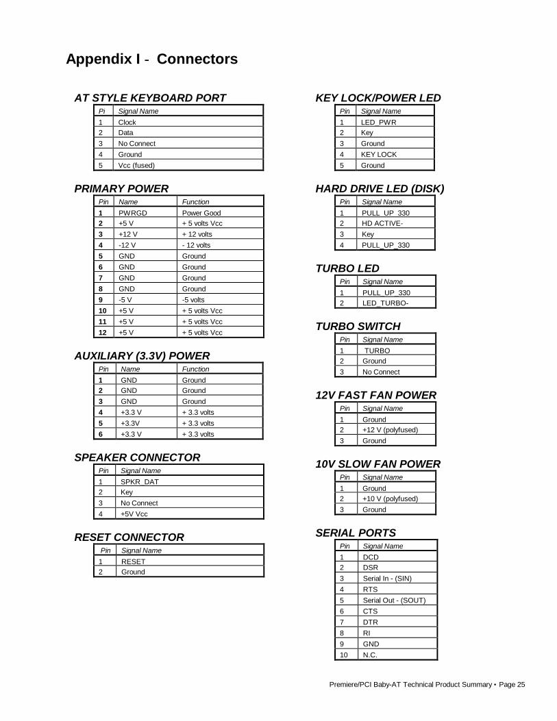
Appendix I − Connectors
AT STYLE KEYBOARD PORTPi Signal Name1 Clock2 Data3 No Connect4 Ground5 Vcc (fused)
PRIMARY POWERPin Name Function1 PWRGD Power Good2 +5 V + 5 volts Vcc3 +12 V + 12 volts4 -12 V - 12 volts5 GND Ground6 GND Ground7 GND Ground8 GND Ground9 -5 V -5 volts10 +5 V + 5 volts Vcc11 +5 V + 5 volts Vcc12 +5 V + 5 volts Vcc
AUXILIARY (3.3V) POWERPin Name Function1 GND Ground2 GND Ground3 GND Ground4 +3.3 V + 3.3 volts5 +3.3V + 3.3 volts6 +3.3 V + 3.3 volts
SPEAKER CONNECTORPin Signal Name1 SPKR_DAT2 Key3 No Connect4 +5V Vcc
RESET CONNECTOR Pin Signal Name1 RESET2 Ground
KEY LOCK/POWER LEDPin Signal Name1 LED_PWR2 Key3 Ground4 KEY LOCK5 Ground
HARD DRIVE LED (DISK)Pin Signal Name1 PULL_UP_3302 HD ACTIVE-3 Key4 PULL_UP_330
TURBO LEDPin Signal Name1 PULL_UP_3302 LED_TURBO-
TURBO SWITCHPin Signal Name1 TURBO2 Ground3 No Connect
12V FAST FAN POWERPin Signal Name1 Ground2 +12 V (polyfused)3 Ground
10V SLOW FAN POWERPin Signal Name1 Ground2 +10 V (polyfused)3 Ground
SERIAL PORTSPin Signal Name1 DCD2 DSR3 Serial In - (SIN)4 RTS5 Serial Out - (SOUT)6 CTS7 DTR8 RI9 GND10 N.C.

Premiere/PCI Baby-AT Technical Product Summary • Page 26
IDE CONNECTORSignal Name Pin Pin Signal Name
Reset IDE 1 2 GroundHost Data 7 3 4 Host Data 8Host Data 6 5 6 Host Data 9Host Data 5 7 8 Host Data 10Host Data 4 9 10 Host Data 11Host Data 3 11 12 Host Data 12Host Data 2 13 14 Host Data 13Host Data 1 15 16 Host Data 14Host Data 0 17 18 Host Data 15Ground 19 20 KeyDRQ3 21 22 GroundI/O Write- 23 24 GroundI/O Read- 25 26 GroundIOCHRDY 27 28 BALEDACK3- 29 30 GroundIRQ14 31 32 IOCS16-Addr 1 33 34 GroundAddr 0 35 36 Addr 2Chip Select 0- 37 38 Chip Select 1-Activity 39 40 Ground
FLOPPY CONNECTORSignal Name Pin Pin Signal Name
Ground 1 2 FDHDINGround 3 4 ReservedKey 5 6 FDEDINGround 7 8 Index-Ground 9 10 Motor Enable A-Ground 11 12 Drive Select B-Ground 13 14 Drive Select A-Ground 15 16 Motor Enable B-Ground 17 18 DIR-Ground 19 20 STEP-Ground 21 22 Write Data-Ground 23 24 Write Gate-Ground 25 26 Track 00-Ground 27 28 Write Protect-Ground 29 30 Read Data-Ground 31 32 Side 1 Select-Ground 33 34 Diskette
PARALLEL PORT CONNECTORSignal Name Pin Pin Signal Name
STROBE- 1 2 AUTO FEED-Data Bit 0 3 4 ERROR-Data Bit 1 5 6 INIT-Data Bit 2 7 8 SLCT IN-Data Bit 3 9 10 GroundData Bit 4 11 12 GroundData Bit 5 13 14 GroundData Bit 6 15 16 GroundData Bit 7 17 18 GroundACJ- 19 20 GroundBUSY 21 22 GroundPE (Paper End) 23 24 GroundSLCT 2 26 N.C.

Premiere/PCI Baby-AT Technical Product Summary • Page 27
ISA CONNECTORSSignal Name Pin Pin Signal Name
GND B1 A1 IOCHK-RSTDRV B2 A2 SD7Vcc B3 A3 SD6IRQ9 B4 A4 SD5-5V B5 A5 SD4DRQ2 B6 A6 SD3-12V B7 A7 SD20WS- B8 A8 SD1+12V B9 A9 SD0GND B10 A10 IOCHRDYSMEMW- B11 A11 AENSMEMR- B12 A12 SA19IOW- B13 A13 SA18IOR- B14 A14 SA17DACK3- B15 A15 SA16DRQ3 B16 A16 SA15DACK1- B17 A17 SA14DRQ1 B18 A18 SA13REFRESH- B19 A19 SA12SYSCLK B20 A20 SA11IRQ7 B21 A21 SA10IRQ6 B22 A22 SA9IRQ5 B23 A23 SA8IRQ4 B24 A24 SA7IRQ3 B25 A25 SA6DACK2- B26 A26 SA5TC B27 A27 SA4BALE B28 A28 SA3Vcc B29 A29 SA2OSC B30 A30 SA1GND B31 A31 SA0
KEY KEYMEMCS16- D1 C1 SBHE-IOCS16- D2 C2 LA23IRQ10 D3 C3 LA22IRQ11 D4 C4 LA21IRQ12 D5 C5 LA20IRQ15 D6 C6 LA19IRQ14 D7 C7 LA18DACK0- D8 C8 LA17DRQ0 D9 C9 MEMR-DACK5- D10 C10 MEMW-DRQ5 D11 C11 SD8DACK6- D12 C12 SD9DRQ6 D13 C13 SD10DACK7- D14 C14 SD11DRQ7 D15 C15 SD12Vcc D16 C16 SD13Master- D17 C17 SD14GND D18 C18 SD15
Premiere/PCI Baby-AT Technical Product Summary • Page 28
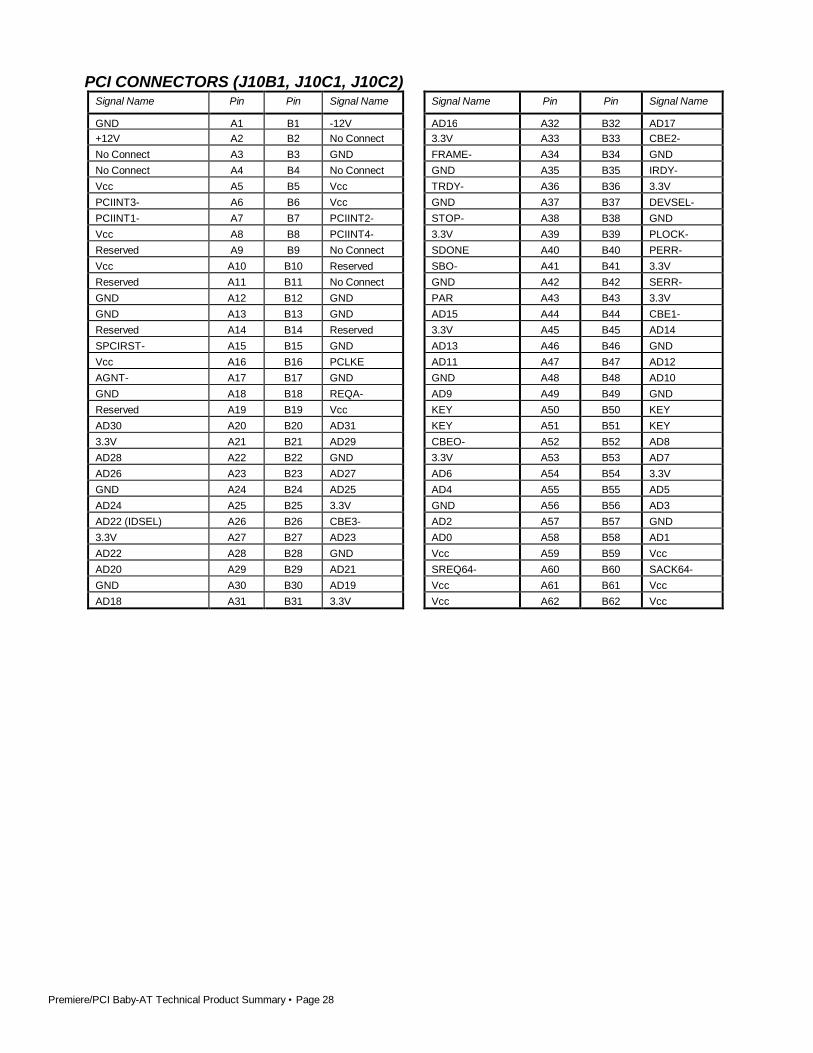
PCI CONNECTORS (J10B1, J10C1, J10C2)Signal Name Pin Pin Signal Name Signal Name Pin Pin Signal Name
GND A1 B1 -12V AD16 A32 B32 AD17+12V A2 B2 No Connect 3.3V A33 B33 CBE2-No Connect A3 B3 GND FRAME- A34 B34 GNDNo Connect A4 B4 No Connect GND A35 B35 IRDY-Vcc A5 B5 Vcc TRDY- A36 B36 3.3VPCIINT3- A6 B6 Vcc GND A37 B37 DEVSEL-PCIINT1- A7 B7 PCIINT2- STOP- A38 B38 GNDVcc A8 B8 PCIINT4- 3.3V A39 B39 PLOCK-Reserved A9 B9 No Connect SDONE A40 B40 PERR-Vcc A10 B10 Reserved SBO- A41 B41 3.3VReserved A11 B11 No Connect GND A42 B42 SERR-GND A12 B12 GND PAR A43 B43 3.3VGND A13 B13 GND AD15 A44 B44 CBE1-Reserved A14 B14 Reserved 3.3V A45 B45 AD14SPCIRST- A15 B15 GND AD13 A46 B46 GNDVcc A16 B16 PCLKE AD11 A47 B47 AD12AGNT- A17 B17 GND GND A48 B48 AD10GND A18 B18 REQA- AD9 A49 B49 GNDReserved A19 B19 Vcc KEY A50 B50 KEYAD30 A20 B20 AD31 KEY A51 B51 KEY3.3V A21 B21 AD29 CBEO- A52 B52 AD8AD28 A22 B22 GND 3.3V A53 B53 AD7AD26 A23 B23 AD27 AD6 A54 B54 3.3VGND A24 B24 AD25 AD4 A55 B55 AD5AD24 A25 B25 3.3V GND A56 B56 AD3AD22 (IDSEL) A26 B26 CBE3- AD2 A57 B57 GND3.3V A27 B27 AD23 AD0 A58 B58 AD1AD22 A28 B28 GND Vcc A59 B59 VccAD20 A29 B29 AD21 SREQ64- A60 B60 SACK64-GND A30 B30 AD19 Vcc A61 B61 VccAD18 A31 B31 3.3V Vcc A62 B62 Vcc

Premiere/PCI Baby-AT Technical Product Summary • Page 29
Appendix J − Environmental Standards
Parameter Condition Specification
Temperature
Non-Operating -40oC to +70oC
Operating +0oC to +55oC
Humidity
Non-Operating 92% Relative Humidity max. @ 36oC
Operating 80% Relative Humidity max. @ 36°C
Altitude
Non-Operating 50,000 feet (15,240 meters)
Operating 10,000 feet (3048 meters)
ESD
1.0kV No Errors
2.5kV No Errors
5.0kV 5% Soft Errors, 0% Hard Errors, No physical damage
7.5kV 10% Soft Errors, 0% Hard Errors, No physical damage
10.0kV 25% Soft Errors, 5% Hard Errors, No physical damage
12.5kV 50% Soft, 10% Hard, No physical damage
15.0kV 100% Soft, 25% Hard, No physical damage
25.0kV 100% Soft, 100% Hard, No physical damage
Shock Non-Operating 30.0G, 11ms, 1/2 sine
Table J-1. Environmental Standards
Appendix K − Reliability DataThe Mean-Time-Between-Failures (MTBF) data is calculated from predicted data @ 55C.
Premiere/PCI Baby-AT baseboard TBD (Testing in progress)

Premiere/PCI Baby-AT Technical Product Summary • Page 30
Appendix L − Early Product FeaturesEarly units of the Premiere/PCI Baby-AT motherboard and Expandable Desktop (code named "Batman"),included several features that differ from those described in this Technical Product Summary. Among them:
BOARD LEVEL FEATURES
CPU
The original motherboard supported only 60 MHz Pentium processors and did not include the voltageregulation circuitry.
REAL TIME CLOCK
The Dallas DS12887 was socketed and could be replaced by the user, if necessary.
IDE
PCI IDE was not integrated on the original Premiere/PCI product. Instead, a PCI IDE paddle card wasused in PCI slot 3 (J10C2, the PCI slot closest to the 3.3V connector) and made use of some of thereserved pins on the PCI interface, as listed in the following table:
Signal Name Pin Pin Signal Name Signal Name Pin Pin Signal Name
GND A1 B1 -12V AD16 A32 B32 AD17+12V A2 B2 STCK (for IDE) 3.3V A33 B33 CBE2-No Connect A3 B3 GND FRAME- A34 B34 GNDSTDI A4 B4 STD0 (for IDE) GND A35 B35 IRDY-Vcc A5 B5 Vcc TRDY- A36 B36 3.3VPCIINT3- A6 B6 Vcc GND A37 B37 DEVSEL-PCIINT1- A7 B7 PCIINT2- STOP- A38 B38 GNDVcc A8 B8 PCIINT4- 3.3V A39 B39 PLOCK-SRSVD1 (for IDE) A9 B9 No Connect SDONE A40 B40 PERR-Vcc A10 B10 SRSVD2 (for IDE) SBO- A41 B41 3.3VSRSVD3 (for IDE) A11 B11 No Connect GND A42 B42 SERR-GND A12 B12 GND PAR A43 B43 3.3VGND A13 B13 GND AD15 A44 B44 CBE1-SRSVD4 (for IDE) A14 B14 SRSVD5 (for IDE) 3.3V A45 B45 AD14SPCIRST- A15 B15 GND AD13 A46 B46 GNDVcc A16 B16 PCLKE AD11 A47 B47 AD12AGNT- A17 B17 GND GND A48 B48 AD10GND A18 B18 REQA- AD9 A49 B49 GNDSRSVD6 (for IDE) A19 B19 Vcc KEY A50 B50 KEYAD30 A20 B20 AD31 KEY A51 B51 KEY3.3V A21 B21 AD29 CBEO- A52 B52 AD8AD28 A22 B22 GND 3.3V A53 B53 AD7AD26 A23 B23 AD27 AD6 A54 B54 3.3VGND A24 B24 AD25 AD4 A55 B55 AD5AD24 A25 B25 3.3V GND A56 B56 AD3AD22 (IDSEL) A26 B26 CBE3- AD2 A57 B57 GND3.3V A27 B27 AD23 AD0 A58 B58 AD1AD22 A28 B28 GND Vcc A59 B59 VccAD20 A29 B29 AD21 SREQ64- A60 B60 SACK64-GND A30 B30 AD19 Vcc A61 B61 VccAD18 A31 B31 3.3V Vcc A62 B62 Vcc
FAN
The Fast Fan/Slow Fan option was not available on the earlier product and there is no jumper.
Premiere/PCI Baby-AT Technical Product Summary • Page 31
SYSTEM LEVEL FEATURES
CHASSIS
A different chassis and front bezel was used for the early Premiere/PCI Expandable Desktop. Thischassis supported only the five peripheral bays accessible from the front panel.
3.5” Bays5.25” Bays
PowerOn/Off
ResetKeylock
SYSTEM KEY LOCK
The earlier version of the chassis included a system keylock. When engaged, the key lock preventskeyboard input. Each system was provided with a set of two identical keys.
RESET SWITCH
The earlier chassis included a reset switch on the front panel.
BACK PANEL
The original product offered a slightly different arrangement of the back panel connections.
Fan Power Keyboard
Expansion SlotsSerial Ports Parallel Port