intel fm2224 24-port 10g ethernet l2 switch chip...intel® fm2224 24-port 10g ethernet l2 switch...
TRANSCRIPT

Intel® FM2224 24-Port 10G Ethernet L2 Switch ChipData Sheet
July, 2008 (Revision 2.3)

Intel® FM2224 24-Port 10G Ethernet L2 Switch Chip Data Sheet
2
Legal
INFORMATION IN THIS DOCUMENT IS PROVIDED IN CONNECTION WITH INTEL® PRODUCTS. NO LICENSE, EXPRESS OR IMPLIED, BY ESTOPPEL OR OTHERWISE, TO ANY INTELLECTUAL PROPERTY RIGHTS IS GRANTED BY THIS DOCUMENT. EXCEPT AS PROVIDED IN INTEL'S TERMS AND CONDITIONS OF SALE FOR SUCH PRODUCTS, INTEL ASSUMES NO LIABILITY WHATSOEVER, AND INTEL DISCLAIMS ANY EXPRESS OR IMPLIED WARRANTY, RELATING TO SALE AND/OR USE OF INTEL PRODUCTS INCLUDING LIABILITY OR WARRANTIES RELATING TO FITNESS FOR A PARTICULAR PURPOSE, MERCHANTABILITY, OR INFRINGEMENT OF ANY PATENT, COPYRIGHT OR OTHER INTELLECTUAL PROPERTY RIGHT. Intel products are not intended for use in medical, life saving, life sustaining, critical control or safety systems, or in nuclear facility applications.
Intel may make changes to specifications and product descriptions at any time, without notice.
Intel Corporation may have patents or pending patent applications, trademarks, copyrights, or other intellectual property rights that relate to the presented subject matter. The furnishing of documents and other materials and information does not provide any license, express or implied, by estoppel or otherwise, to any such patents, trademarks, copyrights, or other intellectual property rights.
The Controller may contain design defects or errors known as errata which may cause the product to deviate from published specifications. Current characterized errata are available on request.
Intel and Intel logo are trademarks or registered trademarks of Intel Corporation or its subsidiaries in the United States and other countries.
*Other names and brands may be claimed as the property of others.
Copyright © 2011. Intel Corporation. All Rights Reserved.

3
Intel® FM2224 24-Port 10G Ethernet L2 Switch Chip Data Sheet
Table of Contents
Overview ........................................................................................................ 4
Document Revision History............................................................................. 4
Product Applicability....................................................................................... 4
Other Related Documents and Tools ............................................................... 51.0 Introduction........................................................................................... 6
1.1 Product Overview ............................................................................61.1.1 Applications .........................................................................61.1.2 Features..............................................................................61.1.3 Ethernet Interface Flexibility ..................................................71.1.4 Control and Test Interfaces....................................................7
1.2 Application Examples .......................................................................81.2.1 Advanced TCA Chassis Switch ................................................81.2.2 Modular/Blade Computer Switch Fabric.................................. 101.2.3 Compute Cluster Interconnect.............................................. 111.2.4 Stackable Workgroup Aggregator Switch ............................... 131.2.5 Applications Summary ........................................................ 14
1.3 Supported Standards and Specifications ........................................... 141.4 Definitions.................................................................................... 14
2.0 Architectural Overview ........................................................................ 162.1 Principles of Operation ................................................................... 162.2 Architectural Partitioning ................................................................ 162.3 In-depth Architecture..................................................................... 18
2.3.1 Clock Domains ................................................................... 182.3.2 Switch Element .................................................................. 202.3.3 Switch Element Scheduler ................................................... 222.3.4 Frame Processing ............................................................... 25
3.0 Functional Description ......................................................................... 273.1 Ethernet Port Logic (EPL)................................................................ 27
3.1.1 Port and Lane configuration ................................................. 273.1.2 SerDes.............................................................................. 283.1.3 SerDes Testing................................................................... 323.1.4 PCS .................................................................................. 343.1.5 IFG Stretch (IFGS) ............................................................. 363.1.6 MAC ................................................................................. 38
3.2 Frame Control............................................................................... 413.2.1 MAC Address Security ......................................................... 413.2.2 IEEE 802.1x - Port Access Control......................................... 413.2.3 VLAN ................................................................................ 413.2.4 Network topology and Spanning Tree Protocol (STP) ............... 443.2.5 Multicast and Protocol Traps ................................................ 443.2.6 MAC Address Table and VLAN Table ...................................... 453.2.7 Lookups and Forwarding...................................................... 463.2.8 Forwarding ........................................................................ 473.2.9 Discard and Monitoring: User-Defined Triggers ....................... 473.2.10 Link-Aggregation................................................................ 493.2.11 Table modification .............................................................. 513.2.12 Memory Integrity ............................................................... 52
3.3 Congestion Management ................................................................ 533.3.1 Priority Mapping ................................................................. 543.3.2 Shared Memory Queues ...................................................... 54

Intel® FM2224 24-Port 10G Ethernet L2 Switch Chip Data Sheet
4
3.3.3 PWD (Priority Weighted Discard) ...........................................563.3.4 Pause Flow Control..............................................................573.3.5 Egress Scheduling...............................................................59
3.4 Statistics ......................................................................................603.5 Management .................................................................................61
3.5.1 Logical CPU Interface ..........................................................633.5.2 Bootstrap Finite State Machine .............................................703.5.3 CPU Interface.....................................................................723.5.4 SPI Interface (EEPROM).......................................................753.5.5 LED Interface .....................................................................763.5.6 TAG ..................................................................................78
3.6 Clocks ..........................................................................................803.6.1 SerDes Clocks, RCK[A:B][1:4]P/N.........................................803.6.2 CPU Interface Clock ............................................................803.6.3 JTAG Clock.........................................................................803.6.4 Frame Handler Clock ...........................................................80
4.0 Electrical Specifications........................................................................824.1 Absolute Maximum Ratings .............................................................824.2 Recommended Operating Conditions ................................................824.3 AC Timing Specifications .................................................................86
4.3.1 CPU Interface, General Timing Requirements..........................874.3.2 JTAG Interface ...................................................................88
5.0 Register Definitions..............................................................................895.1 Register Conventions......................................................................895.2 Register Map .................................................................................895.3 Global Registers ............................................................................94
5.3.1 Global Register Tables .........................................................945.4 Switch Configuration ......................................................................99
5.4.1 Critical Events ....................................................................995.4.2 System Configuration ........................................................1035.4.3 Per port Configuration .......................................................1075.4.4 Non-IEEE 802.3 Header info ...............................................1095.4.5 Switch Control Tables ........................................................1115.4.6 Port Trunk Registers (Link-Aggregation)...............................1155.4.7 Filtering and Monitoring .....................................................117
5.5 Congestion Management...............................................................1195.5.1 Priority Mapping ...............................................................1195.5.2 Queue Management - PWD ................................................1205.5.3 Switch Latency .................................................................125
5.6 Statistics ....................................................................................1265.6.1 Statistics Registers............................................................1265.6.2 Counter groups.................................................................127
5.7 EPL Registers ..............................................................................1335.7.1 SERDES Registers .............................................................1335.7.2 PCS Registers...................................................................1365.7.3 MAC Registers ..................................................................1405.7.4 Scan Registers .................................................................146
6.0 Signal, Ball, and Package Descriptions ...............................................1476.1 Package Overview........................................................................1476.2 Power Mapping ............................................................................1476.3 Interface Mapping........................................................................1486.4 Signal Descriptions.......................................................................149
6.4.1 FM2224 Signals ................................................................1506.4.2 Power Supply Pins and Recommendations ............................155

5
Intel® FM2224 24-Port 10G Ethernet L2 Switch Chip Data Sheet
6.4.3 Recommended Connections ............................................... 1556.4.4 Ball Assignment ............................................................... 156
6.5 Package Dimensions .................................................................... 1716.6 Power Dissipation and Heat Sinking ............................................... 173
6.6.1 Power Dissipation ............................................................. 1736.6.2 Heat Sinking.................................................................... 1746.6.3 Temperature Sensor Operation........................................... 176
7.0 Document Revision Information ........................................................ 1787.1 Nomenclature ............................................................................. 1787.2 Rev 1.0 to 1.1 changes ................................................................ 1787.3 Rev 2.0 to 2.1 changes ................................................................ 1797.4 Rev 2.1 to 2.2 changes ................................................................ 1797.5 Rev 2.2 to 2.3 changes ................................................................ 180

Intel® FM2224 24-Port 10G Ethernet L2 Switch Chip Data Sheet
6
Overview
Intel® intends to offer multiple market- and customer-specific product variants based on the platform. This preliminary data sheet documents the features and functionality of the initial 24-port variant of the FM2000 platform, which will be referred to in this document as the FM2224.
Document Revision History
Product Applicability
This preliminary data sheet documents the features and functionality of the FM2224, the initial member of the FM2000product family. The FM2224 part number is structured as follows:
Key:• Product Family: “2” represents the Ethernet L2 switch product family, of which the
FM2000 is a member.• Port Configuration: Provides guidance on the composition of the ports in the device,
as follows:• 1: More than 50% of the interfaces are single-SerDes interfaces• 2: More than 50% of the interfaces are quad-SerDes interfaces• Aggregate Bandwidth: “24” represents an aggregate bandwidth of 240Gbps.
Revision Date Notes
1.0 Oct 25, 2006 Initial version of Preliminary Datasheet
2.0 July 31, 2007 Updates per section 7.2
2.1 Oct 1, 2007 Updates per section 7.3
2.2 April 17, 2008 Updates per section 7.4
2.3 July 17, 2008 Updates to FRAME_TIME_OUT, CPU timing notes and LED section.

7
Intel® FM2224 24-Port 10G Ethernet L2 Switch Chip Data Sheet
• Temperature: “C” represents Commercial temperature grade. The grades indicate case temperatures as follows:
RoHS Compliance: The presence of a “-G” means that the device is compliant with the RoHS requirements for restrictions on the use of hazardous substances. Compliance is via exemption #15 in the RoHS Directive Annex, which allows for the use of Pb (lead) in the solder bumps used for die attaché in flip-chip packages. -G parts have lead-free solder balls on the exterior of the package for PC board die attach.
Note that the non-RoHS compliant package meets the RoHS limits for the other five substances, but contains Pb in the external solder balls, which is not allowed by the RoHS directive, and in the solder bumps for die attach.
Other Related Documents and Tools
Other documents that may be useful for evaluating and using the FM2224 include:
• FM2224 Software API Specification• FM2224 Specification Update, which contains errata and other specification and
documentation changes• FM2224 Design and Layout Guide• FM2224 Reference Design Data Sheet• FM2224 Design Support Package on CD
Grade Designator Tcase(min) (ºC)
Tcase(max) (ºC) Commercial -C
0 +85 Extended
-E 0 +105
Industrial -I -40
+115
Intel® FM2224 24-Port 10G Ethernet L2 Switch Chip Data Sheet
8
1.0 Introduction
1.1 Product Overview
The FM2224 is a fully-integrated, single-chip 24-port 10G Ethernet layer-2 switch chip that offers wire-speed performance, extremely low-latency characteristics, and leading power efficiency. With its robust layer-2 switching capabilities and the ubiquity of Ethernet, the FM2224 fits comfortably in a number of existing and emerging applications. And, with the unprecedented level of integration, the FM2224 removes the cost, area, and power barrier for rapid and far-reaching 10G Ethernet deployment.
1.1.1 Applications
With unprecedented integration, performance, power efficiency, and latency characteristics, the FM2224 can be used for a variety of infrastructure and interconnect applications, some of which include:
• Blade computer and IP storage platform internal fabric• Data center cluster interconnect (clustered computers and storage resources)• Enterprise stackable switch (performance workgroups and workgroup aggregation)• AdvancedTCA backplane fabric (star or mesh architecture)• AdvancedTCA carrier card switch (interconnecting mezzanine cards)• Proprietary system backplane fabric
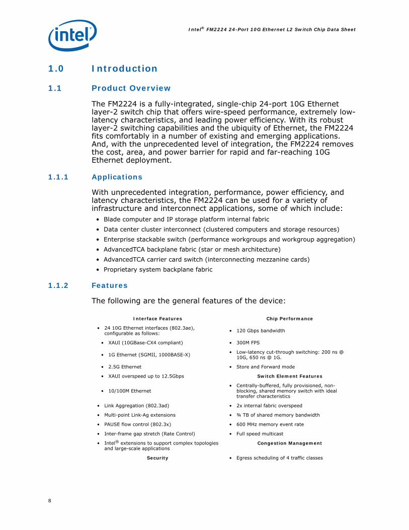
1.1.2 Features
The following are the general features of the device:
Interface Features Chip Performance
• 24 10G Ethernet interfaces (802.3ae), configurable as follows: • 120 Gbps bandwidth
• XAUI (10GBase-CX4 compliant) • 300M FPS
• 1G Ethernet (SGMII, 1000BASE-X) • Low-latency cut-through switching: 200 ns @ 10G, 650 ns @ 1G.
• 2.5G Ethernet • Store and Forward mode
• XAUI overspeed up to 12.5Gbps Switch Element Features
• 10/100M Ethernet• Centrally-buffered, fully provisioned, non-
blocking, shared memory switch with ideal transfer characteristics
• Link Aggregation (802.3ad) • 2x internal fabric overspeed
• Multi-point Link-Ag extensions • ¾ TB of shared memory bandwidth
• PAUSE flow control (802.3x) • 600 MHz memory event rate
• Inter-frame gap stretch (Rate Control) • Full speed multicast
• Intel® extensions to support complex topologies and large-scale applications
Congestion Management
Security • Egress scheduling of 4 traffic classes
9
Intel® FM2224 24-Port 10G Ethernet L2 Switch Chip Data Sheet
1.1.3 Ethernet Interface Flexibility
The FM2224 contains 24 interfaces, each of which can be independently configured to support one of the following modes:
• 10G Ethernet: XAUI interface, with 10GBase-CX4 compliance (accomplished with four SerDes pairs operating at 3.125 GHz, with 8b/10b encoding)
• 2.5G Ethernet: Pre-standard implementation (accomplished with a single SerDes pair operating at 3.125 GHz, with 8b/10b encoding)
• 1G Ethernet: SGMII and 1000BASE-X compliance (accomplished with a single SerDes pair operating at 1.25 GHz, with 8b/10b encoding)
• User-configurable mode: The FM2224 can support two input reference clocks, each operating up to 400 MHz. Each of the device's 24 interfaces can independently select one of the two reference clocks. Additionally, each interface can be configured to have one or four SerDes pair(s) active. So, as an example, given two input clocks of 312.5 MHz and 400 MHz, each interface can be independently configured to support data rates of 2.5 Gbps, 3.2 Gbps, 10 Gbps, and 12.8 Gbps.
When all interfaces are set to the same operating mode, the FM2224 performs as a cut-through switch. When interfaces are configured for different modes, the FM2224 performs a store-and-forward function on the link pairs that don't have matching clock rates to avoid buffer over-runs and other congestion due to interface rate mismatch.
1.1.4 Control and Test Interfaces
The FM2224 also contains a standard 32-bit address/data processor bus interface that is used to read and write all Control Status Registers that control the chip configuration and operation, and also to obtain status and to debug the chip. This CPU interface can be configured to support a variety of commercial processors including the Motorola MPC8260, and MPC860, IBM PowerPCs with an EBC bus, and various I/
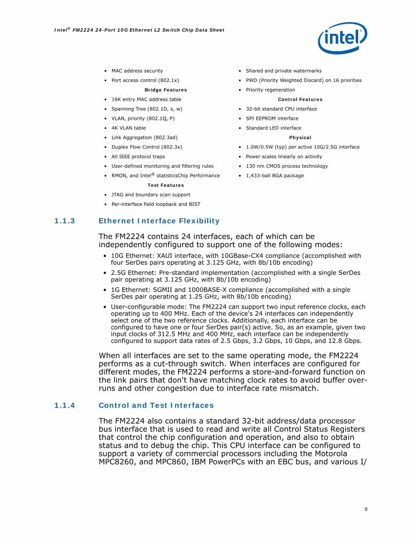
• MAC address security • Shared and private watermarks
• Port access control (802.1x) • PWD (Priority Weighted Discard) on 16 priorities
Bridge Features • Priority regeneration
• 16K entry MAC address table Control Features
• Spanning Tree (802.1D, s, w) • 32-bit standard CPU interface
• VLAN, priority (802.1Q, P) • SPI EEPROM interface
• 4K VLAN table • Standard LED interface
• Link Aggregation (802.3ad) Physical
• Duplex Flow Control (802.3x) • 1.0W/0.5W (typ) per active 10G/2.5G interface
• All IEEE protocol traps • Power scales linearly on activity
• User-defined monitoring and filtering rules • 130 nm CMOS process technology
• RMON, and Intel® statisticsChip Performance • 1,433-ball BGA package
Test Features
• JTAG and boundary scan support
• Per-interface field loopback and BIST

Intel® FM2224 24-Port 10G Ethernet L2 Switch Chip Data Sheet
10
O bridge chips (such as the PLX 9030 PCI bridge chip from PLX Technologies). The different modes are supported through pin strapping options. This CPU interface operates up to 100 MHz.
Additionally, the FM2224 contains an LED interface that can be connected to external LED driver chips to provide port- and system-level status and activity via front-panel LEDs.
Lastly, the FM2224 implements an industry-standard JTAG controller for test and design debug. The JTAG controller can access boundary scan registers and all internal registers.
1.2 Application Examples
With unprecedented integration, performance, power efficiency, and latency characteristics, the FM2224 can be used for a variety of infrastructure and interconnect applications, some of which include:
• Blade computer and IP storage platform internal fabric• Data center cluster interconnect (clustered computers and storage resources)• Enterprise stackable switch (performance workgroups and workgroup aggregation)• Advanced TCA backplane fabric (star or mesh architecture)• Advanced TCA carrier card switch (interconnecting mezzanine cards)• Proprietary system backplane fabric
The FM2224 is a versatile device that can be used in a variety of applications where efficient Ethernet packet switching is the method of choice for interconnecting the elements in a system. The following subsections detail some of the common applications that the FM2224 is capable of supporting, and identifies some of the device's capabilities that are relevant for each application.
1.2.1 Advanced TCA Chassis Switch
The FM2224's high level of integration (high port count) makes it a great fit for the Advanced TCA chassis (including the 14-slot, 19”-rack version and the 16-slot, 23”-rack version, as well as the smaller variants). With 24 ports, the device can physically support any common switching method: central switch fabric (dual star or dual-dual star), fully-meshed backplane, and replicated meshes.
1.2.1.1 Central Switch Fabric
In this application, typically two slots in the chassis are populated with switch fabric cards that provide point-to-point connections to all other cards in the chassis. The two switch elements can be configured to either load balance or to provide fail-over redundancy. In some cases, available switch ports are used for uplinks to other systems outside of the platform.

11
Intel® FM2224 24-Port 10G Ethernet L2 Switch Chip Data Sheet
Figure 1. Advanced TCA Central Switch Fabric
Key Capabilities• Link aggregation on the uplink ports• Interfaces configurable for 1G Ethernet support for glueless connection to the 1G
Ethernet base fabric• Fail-over redundancy from one switch element to the other, using a method of
polling status information between the two switch elements, and rapidly switching traffic from one element to the other.
1.2.1.2 Fully-Meshed Backplane
In this application, each node card contains an FM2224 that connects that card with every other card in the chassis in a full 10G mesh configuration. The remaining switch ports are used to provide switching between all of the elements on the node card (e.g., interconnection between Advanced Mezzanine Cards on a Carrier Card). This example combines the full mesh architecture with the Advanced Mezzanine Card (AMC) architecture. With 24 ports, the FM2224 offers optimal connectivity between all of the system cards, providing the most flexible, scalable, and resilient base architecture for building virtually any kind of communications or computing system.

Intel® FM2224 24-Port 10G Ethernet L2 Switch Chip Data Sheet
12
Figure 2. Advanced TCA Node Card Switch (Full Mesh)
Key Capabilities• Mesh-based address resolution, where connections between switch elements are
terminated at the endpoints.• Similarly for multicast and broadcast traffic, switch elements can propagate
multicast and broadcast traffic received from another slot only to its local endpoints - to avoid self-inflicted broadcast storms.
1.2.2 Modular/Blade Computer Switch Fabric
Blade computing has exploded onto the scene in recent years as a cost-effective and scalable method for building large-scale computing and storage infrastructures. And, Ethernet is emerging as the de facto method for interconnecting compute components in the chassis. The FM2224's low latency and high level of integration make it a perfect complement to the emerging endpoint devices that are more-and-more efficiently converting Ethernet to CPU-native interfaces (such as PCI Express, HyperTransport, and RapidIO).
Figure 3 shows a simple example of a multi-host computing platform that leverages switched Ethernet as the local host-to-host interconnection as well as the external link to other computer room systems.

13
Intel® FM2224 24-Port 10G Ethernet L2 Switch Chip Data Sheet
Figure 3. Blade Computer Switch Fabric
Key Capabilities
Low latency.• Multiple uplinks providing redundant (or load-balanced) connections to the rest of
the computer room. On link failure, the ability to efficiently and automatically switch traffic (or migrate active traffic) to the remaining link.
• Traffic classes, and enforcement of priorities, to efficiently intermix transaction and data types (e.g., bursty network access with local streaming to disk or tape).
• Ethernet extensions enabling support of advanced topologies, such as mesh and fat trees.
1.2.3 Compute Cluster Interconnect
In this example, the FM2224 is used as the core of an Ethernet switch optimized for efficiently interconnecting multiple compute systems in a cluster. For cluster computing, latency, performance, resiliency, and scalability are the key factors.

Intel® FM2224 24-Port 10G Ethernet L2 Switch Chip Data Sheet
14
Figure 4. Compute Cluster Switch
The FM2224 can address scalability, resiliency, and system-level performance by supporting fat-tree (federated switch) architectures, as is shown in Figure 5. In this example, 96 10G Ethernet ports are available for interconnecting compute resources, without introducing any blocking.
Figure 5. Fat-Tree Configuration of Cluster Switches
The same system architecture can be implemented in a single chassis, providing additional cost reduction, modularity, and resiliency. Figure 6 shows an example of a 96-port 10G Ethernet switch platform with CX-4 interfaces, using 12 FM2224 chips. Similarly, a 144-port system can be configured with 18 chips and a 288-port system with 36 chips.

15
Intel® FM2224 24-Port 10G Ethernet L2 Switch Chip Data Sheet
Figure 6. Fat-Tree Configuration in a Box
Key Capabilities• Low end-to-end latency.• Hardware extensions, such as multi-port link aggregation and uplink/downlink port
association, that allow fat-tree connectivity without creating unwanted loops.• Ports can operate at 1Gbps for mixed-speed applications
1.2.4 Stackable Workgroup Aggregator Switch
The compute cluster switch (perhaps with different port configurations and interface options) can be used as a cost-effective method for aggregating dense workgroups of 10/100/1000 Ethernet users. The FM2224 can support VLANs and VLAN stacking to preserve workgroup and user associations.
This example shows the same stackable switch being deployed as an aggregator of multiple 10/100/1000 workgroup switches.
Figure 7. Aggregator for Stackable 10/100/1000 Switch
Key Capabilities

Intel® FM2224 24-Port 10G Ethernet L2 Switch Chip Data Sheet
16
• Link aggregation, with the ability to aggregate the uplink ports as well as multiple instantiations of two user ports (to support either link redundancy or higher throughput links) to each connected stackable switch.
• VLAN preservation and stacking to maintain workgroup separation as defined by the workgroup switches.
1.2.5 Applications Summary
Summarizing, with a rich set of features, and unprecedented performance and integration, the FM2224 can be used cost-effectively (and to deliver differentiation) in a variety of Ethernet switching applications in both the communications and computing markets. And, as is the case with Advanced TCA, the FM2224 can provide a platform for accelerating the convergence of the two markets and related applications.
1.3 Supported Standards and Specifications
The following standards and specifications are supported by (or otherwise relevant to, as noted) the FM2224:
IEEE
802.3• 802.3-2002• 802.3ae• 802.3z• 802.3ak (CX4)• 802.3ad
802.1• 802.1D (2004)• 802.1Q (2003)• 802.1p• 802.1s• 802.1w• 802.1X
1.4 Definitions
The following are terms that are relevant for the FM2224, and which are used throughout this document to describe the features, functions, configuration, and use of the FM2224.Interface Generic term referring to a single logical implementation
containing a transmit and receive data path. The FM2224 contains several interface types (XAUI, JTAG, CPU, LED, etc.).

17
Intel® FM2224 24-Port 10G Ethernet L2 Switch Chip Data Sheet
Port Refer to the definition of “Interface” above. Used interchangeably with “interface”, although used more frequently to identify a specific physical implementation - rather than a generic logical implementation. As examples of how both are used: “The FM2224 contains 24 10G Ethernet interfaces”; “Make sure the port is enabled before sending data”.
XAUI Ten-Gigabit Attachment Unit Interface, defined by the IEEE as an interface extender for XGMII (the ten-Gigabit Media Independent Interface).
CX4 Used generically in this document to refer to the ten-Gigabit copper interface extensions made to XAUI (and defined by IEEE as 10GBase-CX4) to support copper “CX4” cables. The interface is intended to connect servers or switches over short distances - up to 50 feet.
CSR (Register) Control Status Register used for configuration, status reporting, and debug.
Nexus Intel's Terabit fully-connected non-blocking crossbar; Nexus is used to make the Terabit non-blocking shared memory switch element.
Queue Conceptually, a temporary packet storage element in the shared memory (a.k.a., FIFO). In the FM2224, each frame has multiple queue associations in the memory, and those associations are used for congestion management and scheduling.
Cut Through A switching mode or architecture where the switch can begin transmitting the packet as soon as the destination port is known, without waiting for the end of the frame to arrive.
Store-and-Forward A switching mode or architecture where the packet is first copied to memory (stored) in its entirety before being delivered (forwarded) to the destination port. This mode is typically used to forward between ports of different speeds or to ensure frames with bad CRC are discarded immediately.

Intel® FM2224 24-Port 10G Ethernet L2 Switch Chip Data Sheet
18
2.0 Architectural Overview
2.1 Principles of Operation
The FM2224 is an IEEE-compliant Ethernet bridge. For an in-depth discussion of the principles of operation, see Clause 7 of the IEEE 802.1D-2004 specification.
2.2 Architectural Partitioning
The FM2000 is architecturally partitioned into five major blocks, as shown in Figure 8. They are:
• Ethernet Port Logic (EPL), RX and TX.• Frame Processor (FP)• Switch Element Data Path (SEDP)• Switch Element Scheduler (SES)• Management (MGMT)
This partitioning was designed specifically to attain high throughput, high port density, low latency, and low power in a single integrated device.
Figure 8. FM2224 Block Diagram

19
Intel® FM2224 24-Port 10G Ethernet L2 Switch Chip Data Sheet
Ethernet Port Logic (EPL)
The Ethernet Port Logic (EPL) is the per-port replicated block. It is purposely designed to be as “thin” as possible to enable the FM2224 to scale -- practically -- to 24 ports. The EPL contains only the essential features to identify a packet and its header, parse the information appropriately, and stream the information to the correct location. The EPL implements the PMA and PCS layers, and it further checks each frame for various errors, including length and frame errors. The packet data is buffered into a 64-byte segment for streaming into the switch element at the Nexus data rate (30 Gb/s per port), beyond which the EPL is purely cut-through. The header is parsed and sent to the frame processor. On TX, the EPL collects tag information from the scheduler and uses that to perform VLAN egress tagging.
Frame Processor (FP)
The Frame Processor (FP) is a centralized and highly-optimized pipeline that implements all of the complex frame relay policy and congestion management functions, and keeps statistics for activity across the entire chip. Once a reservation has been set, the frame processor pipeline is deterministic, producing one header per clock, and no further queuing is required. It takes a header as its input and produces a forwarding mask 6 clocks later - at full line rate for up to 24 ports. It processes the destination MAC address, source MAC address, VLAN, and Spanning Tree protocol. In addition, it checks security and reserved traps, and updates the MAC Address table. It receives queue status from the switch element scheduler and determines whether to discard frames or pause inputs on a frame's ingress. And finally it manages the link aggregation groups.
Switch Element Data Path (SEDP)
The switch element is a fully-provisioned, centrally-buffered switch with ideal transfer characteristics. It consists of the switch element datapath and scheduler.
The Switch Element Data Path (SEDP) is a shared memory structure constructed from Intel's proprietary crossbar and memory technology. The memory delivers approximately three-quarters Tb/s of bandwidth, necessary to support sustained transfer of the worst segment corner case of 65-byte frames. Though it uses crossbars it is not a “crossbar-based” switch; it is centrally buffered. On ingress, frames are streamed in from the 24 EPLs through a crossbar, in a non-blocking fashion, to 16 banks of 64 kB of memory (1 MB total), where they are kept while the headers are queued and scheduled. Each 64-byte segment from the EPL is striped across the 16 32-bit banks of memory (512 bits at a time). Another crossbar then connects the 16 banks of memory back
Intel® FM2224 24-Port 10G Ethernet L2 Switch Chip Data Sheet
20
out again to the 24 ports on egress, permitting a non-blocking transmission of scheduled frames, with no multicast replication bottlenecks.
Switch Element Scheduler (SES)
The Switch Element Scheduler (SES) manages the frame data in the switch element datapath and communicates with the frame processor and switch element datapath. It performs a time-sliced arbitration algorithm to schedule frames streaming across the ingress crossbar. It then represents the frame as a linked list of pointers that may exist anywhere in the memory, allocating pointers on ingress, and freeing pointers on transmission. (A pointer points to a group of four segments, allowing a maximum of 4096 packets in the switch at one time.) The SES queues out-of-band frame information that travels along with the packet and comes from the frame processor, and it queues the segment pointers. It manages multicast replication, as pointers are forwarded from an RX queue to a TX queue. Frames marked with errors, from either the EPL or the FP, are discarded if the frame has not yet been transmitted. If the frame has been partially transmitted, then it is forced to have a bad CRC. The frames are scheduled for egress transmission according to a number of selectable algorithms, including strict priority and weighted round robin. Frames are associated with three queues: RX port, TX port, and shared memory. The queue status is reported to the frame processor for its use in congestion management decisions for pause and discard.
Management (MGMT)
The Management block (MGMT) contains slow interfaces to access and configure the device. It allows the FM2224 to communicate with a host. There is an internal management bus that matches the slow rate of the management interface to all of the different high-speed blocks in the device. The management block cannot get involved with the actual line rate forwarding activity, but it otherwise has a high degree of visibility into the device.
2.3 In-depth Architecture
This section is intended for the curious system architect who wants to understand and/or validate the performance of FM2224 with an in-depth analysis of the architecture. This section is not necessary to successfully operate the FM2224.
2.3.1 Clock Domains
The FM2224 is based on the model of GALS (globally asynchronous locally synchronous). In this model, a fundamental block is built with a standard ASIC design process, creating a synchronous fixed-function block. These blocks employ a protocol on their interfaces that allows

21
Intel® FM2224 24-Port 10G Ethernet L2 Switch Chip Data Sheet
them to safely communicate without a specified event rate or phase relationship to other blocks. From the system-level perspective one block's synchrony is contained entirely within the block itself, forming fully-independent clock domains. This allows each block to run at the optimal clock rate for its function, for example 312.5 MHz Ethernet Port Logic (EPL), 270-360 MHz Frame Processor (FP), and 66 MHz Management (MGMT) logic. There are no timing constraints between the blocks; they are truly independent oscillators in both frequency and phase.
There are three independent synchronous blocks in the FM2224:• Ethernet Port Logic (EPL)• Frame Processor (FP)• Management unit (MGMT)
The EPL is replicated 24 times in the design. Thus there are 26 independent clock domains (excluding blocks used for test). Each EPL can operate up to 400 MHz. The FP pipeline operates at 270 MHz to 360 MHz, depending on the frame rate chosen. The Management block operates at 33 MHz to 66 MHz, which is user selectable. There are no per-frame actions performed by the Management block, except frames sent or received from the host.
Intel's high-performance logic and memory is used to implement the asynchronous interconnect between the clock domains, where it provides a performance and integration advantage.
There are four significant asynchronous logic blocks:• Header aggregator - interconnect between EPL and FP pipeline• MAC address table• Switch Element Data Path• Switch Element Scheduler
The header aggregator serializes the header processing requests of 24 EPLs to the FP so that logic for the extensive Ethernet features are instantiated once at a required processing rate of 270-360 MHz. The EPL sends two messages per frame, one at the beginning of the frame with the header information and one at the end of the frame that signals frame length and error conditions. These requests appear at a worst-case event rate of 540-720 MHz. They appear non-deterministically, given the independent clock domains of the EPL, and they must be arbitrated into a single frame processing pipeline. Since the average-case packet rate is a factor of 10-20 less then the worst case packet rate in Ethernet, this asynchronous circuitry greatly improves frame processing latency and reduces power - the circuit can support the worst-case event rate, but doesn't consume power unless it is active, and then only to the extent that it is active.

Intel® FM2224 24-Port 10G Ethernet L2 Switch Chip Data Sheet
22
The MAC Address table contains 16K - 12-byte MAC address lines. Both the destination and source addresses are searched each packet creating an event rate of 540-720 MHz on a 176 KB memory, excluding learning updates. The table is therefore implemented asynchronously, leveraging Intel's high performance memory.
The Switch Element Data Path and Scheduler are based on 1 GHz crossbars and 600 MHz asynchronous SRAMs. This circuitry has very little protocol calculations, and must meet challenging throughput and latency goals while dissipating little power.
2.3.2 Switch Element
Figure 9. FM2224 Switch Element Architecture
2.3.2.1 Shared Memory
A frame is stored as a linked list of separate fixed-size non-consecutive segments of memory. The switch element makes no restrictions on which ports may use what memory locations. The ingress port is given pointers to these segment locations as they free up and as the port needs them. The frame is streamed into memory and stored while the switch makes its forwarding decision. The frame is then scheduled to none, one or many egress ports.
23
Intel® FM2224 24-Port 10G Ethernet L2 Switch Chip Data Sheet
The segment size and segment block size are important in determining the required performance of the switch element and in understanding the maximum storage capacity of the switch. A frame is processed 64 bytes at a time. The absolute worst-case segment rate occurs when all frames are 65 bytes in length and all ports are utilized at 100% capacity. This creates a segment rate of 720 MHz for a 24-port switch, assuming minimum inter-frame gap. A memory pointer references a block of four segments, or 256 bytes. Any frame that is less than 256 bytes will still consume 256 bytes of memory. In general, the memory that a frame consumes is its frame length rounded up to an integral multiple of 256 bytes. The switch element meets the minimum processing rates for frames, segments, and segment blocks to be fully provisioned in the theoretical worst case of 24 ports. The FM2000 may hold up to 4K frames at any one time assuming the aggregate frame storage does not require more than 4K segment blocks.
The circuit-level architecture challenge arises from the requirements:• 0.723 Tb/s shared memory bandwidth• 240 Gb/s second cross-sectional bandwidth (183.5 Gb/s for 65 byte frames)• Read + Write any memory element every cycle• Frame/segment granularity efficiency (51% worst case)• Low latency application requirement• 1 MB of on-chip frame memory• Modest power budget• Modest area budget
Significant parallelism and careful striping makes the challenge feasible with Intel's high-performance memory technology. Without introducing any corner cases, the memory may be written 512 bits at a time across 16 32-bit banks of memory. This brings the 0.723 Tb/s memory requirement down to a 706 MHz event rate (accounting for both a read and a write). Increasing the cell size to 128 bytes and striping across a 1024-bit memory would reduce the maximum segment rate down to 402 M segments per second (still requiring > 400 MHz memory), but at the cost of an extra 51.2ns in latency, an increase in the total required memory bandwidth to 0.825 Tb/s and a doubling of the crossbar port count and wiring.
2.3.2.2 SRAM and Crossbar Building Blocks
Intel's asynchronous SRAMs and crossbars provide key advantages to meeting the challenge of doing a low latency Tb/s shared memory.
The fundamental unit of any shared memory switch is the SRAM building block. In the FM2000, this is a 16 kB memory consisting of 4000 lines of 32-bit words. It is based on foundry-provided standard and reliable 6T SRAM state bits. With custom logic, the overall SRAM achieves > 600 MHz per single-ported bank. Frame memory must be

Intel® FM2224 24-Port 10G Ethernet L2 Switch Chip Data Sheet
24
read and written once per cycle, often requiring the use of dual-ported SRAM. However, in the FM2000, the 600+ MHz single-ported performance is converted into worst-case 300+ MHz read + write. There is an additional performance gain in banking buses internal to the SRAM block, but it is not relied on in worst-case calculations.
Single-ported memory is much smaller and more reliable than multi-ported memory structures, leading to a significantly more manufacturable device.
The required bandwidth in a dense 10G shared-memory switch is so high that buses are no longer adequate. Crossbars create private point-to-point connections between the port logic and the memory banks. They provide increased bandwidth and reduced power over bus-based architectures.
The FM2000 Switch Element Data Path uses Intel's Nexus crossbar, an asynchronous circuit with many significant properties:
• 24 Gb/s per port cross-sectional bandwidth• 3 ns fall-through latency including link initialization and tear-down• Area approximately 20x smaller than an SoC interconnect implemented with a
standard flow• Power dissipation that scales with usage only; no overhead but leakage. And power
that is significantly less than the power of a shared bus.
The bandwidth requirement on the crossbar is different from that in the SRAM. The crossbar delivers the 64-byte segment to the memory in 1/(segment rate) = 33.6 nS. For a 32-bit datapath, the delivery of the segment takes 16 cycles, or a performance requirement of 476 MHz port speed.
The GHz crossbars in the FM2000 have about 2x more bandwidth than is necessary to meet worst-case event rates. This overspeed is useful. It reduces overall latency and provides added margin. In addition, it enables a high bandwidth mode in which performance is met statistically. This allows the device to be run at lower voltage for applications that are more sensitive to power than theoretical worst-case guaranteed performance.
2.3.3 Switch Element Scheduler
The scheduler performs the following functions:• Tracks pointers• Arbitrates packet entry into the Switch Element Data Path• Receives per-frame information from the Frame Processor• Schedules frames from Rx queues to TX queues based on forwarding decisions,
including TX multicast replication• Provides egress scheduling of frames per TX output.
25
Intel® FM2224 24-Port 10G Ethernet L2 Switch Chip Data Sheet
• Delivers out-of-band information to Ethernet Port Logic, such as new VLAN tag, source port, etc.
• Spools segments during frame transmission• Frees segments after transmission and re-allocates them to new frames • Reports the status of the pointers as they contribute to global shared occupancy,
RX port and TX port association, for use in the congestion management calculation in the frame processor
• Provides rate matching between different speed ports
Figure 10. Switch Element Scheduler
2.3.3.1 Ingress Arbitration
When a frame first arrives at the Switch Element Scheduler, an arbitration request is started for access into the switch, since in the general case multiple ports could have pointers that refer to the same bank of memory. Once that arbitration is granted, a “time slot” is granted to the port. Each consecutive bank of memory is then scheduled in order during the entire frame transmission. Thus the only arbitration and statistical delay occurs at the head of the frame. The arbitration loop cycles through all 24 ports in a worst-case timing of 33.6 nS. This comes from assuming the worst-case segment rate on all ports, and leads to a requirement that the segment scheduler operates at 720 MHz or greater. The arbitration delay adds 33.6 nS of fall-through latency in the worst case, but in the average case, and with the overspeed built into the system, it adds less than 10 nS.
Intel® FM2224 24-Port 10G Ethernet L2 Switch Chip Data Sheet
26
2.3.3.2 Congestion Information
The segment utilization is reported for RX and TX ports. And the amount of memory that is deemed to be “shared” is also reported to the Frame Processor for congestion management. To reduce the event rates of the congestion management calculation, the granularity of this reporting is on 1 kB blocks (16 segments).
2.3.3.3 Rate Matching and Cut-Through
The Switch Element Data Path natively handles matching rates of varying ports. However, as a limitation of Ethernet, when a slower port talks to a faster port, that transaction must be performed in store-and-forward mode to avoid Tx FIFO under-run. Accordingly, there is an N-squared 1-bit matrix which configures whether each port pair should be scheduled in cut-through mode or store-and-forward mode. The switch element is natively cut-through, but when the bit for the port-pair-direction is set, the “store-and-forward” process of Figure 10 allows the switch element to delay egress scheduling until the entire frame has entered memory.
2.3.3.4 Rx and Tx Queues
A frame is eligible and its pointers are placed in “Rx queues” once it has passed the “store-and-forward” process having either one complete 64-byte segment in the Switch Element Data Path in cut-through mode, or the entire frame in the data path in store-and-forward mode. There is adequate storage in Rx queues for all of 4000 frames (the maximum) to be stored in the switch element with their pointers in Rx queues.
Once the destination is known from the frame processor, the pointers in Rx queues are forwarded to Tx queues. While a multicast frame only ever exists in one place in the frame memory, the pointer to that frame is replicated for each port in Tx queues. This is done such that it is always possible to saturate all of the output bandwidth of the switch with multicast traffic while continuing to receive full rate.
Once all of the pointers in Tx queues that refer to the same frame have an indication for transmission, then the memory segments for that frame are freed, and new frames may occupy the memory locations.
2.3.3.5 Egress Scheduling
The “QCache” process in Figure 10 schedules the next frame for transmission. It walks through all of the ports on the same 33.6 nS time cycle as the ingress arbitration. There are 96 queues in the “QCache” of a 24-port the FM2000 device because there are four fabric priorities for each output port. The next frame of all 96 queues is stored in Qcache. This caching is necessary to reduce the latency through the scheduler, and to meet the frame rate of scheduling 270-360 M frames per second.

27
Intel® FM2224 24-Port 10G Ethernet L2 Switch Chip Data Sheet
2.3.4 Frame Processing
The frame processing pipeline is architected to achieve two performance goals and organized to implement efficiently the complex Ethernet features in the FM2000. It forwards one frame per clock at a maximum rate of 360 MHz. It produces its forwarding decision with less latency than it takes to store the first segment of the frame into the switch element for most traffic patterns. Thus the processing of the Ethernet features above the PCS layer of the protocol don't affect the latency of the FM2000. The frame processing pipeline is shown in Figure 11.
The aggregation of frame handling requests from the EPL and the lookups are performed in the Lookup sub-block of the frame processor. There are four lookups per frame: source address and destination address in the MAC address table, and VLAN and Spanning Tree state in the VLAN ID table. This requires a maximum data rate of 720 MHz for a fully-provisioned 24-port device. All of the table data is loaded and then passed directly to the Frame Handler to determine the action on the frame. From time to time, learning requests come back from the Frame Handler to the Lookup. A forwarding decision in cut-through mode happens before a good CRC is known. A learning event only happens after a frame is known to have a good CRC. Learning can happen at line rate under most circumstances. However in general usage models it only needs about a KHz frequency.
The Frame Handler is an ASIC-based rules machine for frame processing. There is a notion of precedence in frame processing. The switch only takes one action on a frame. So if a frame is discarded because the port is in the spanning tree discard state, it does not matter, and it is not tracked, if there are other violations associated with the frame. Any action that the frame processor takes is counted in the Statistics block. There is full RMON support in the Statistics block, as well as statistics for all of the FM2000's custom features. There are 13 independent groups of statistics. No more than one counter in a group is updated per frame. All of the statistics are gathered in such a way that they never experience an event greater than the maximum frame rate of the FM2000. All statistics are 64 bits so that there are no event rate requirements on the rate at which the CPU polls the statistics.

Intel® FM2224 24-Port 10G Ethernet L2 Switch Chip Data Sheet
28
Figure 11. FM2000 Frame Processor Architecture

29
Intel® FM2224 24-Port 10G Ethernet L2 Switch Chip Data Sheet
3.0 Functional Description
This section describes in detail the features and functions supported by the FM2224. For a detailed description of the unit-level partitioning of the device, see Figure 8 Section 2.0.
3.1 Ethernet Port Logic (EPL)
The FM2224 contains 24 Ethernet Port Logic transmit and receive pairs; each pair contains the SerDes, PCS, and a portion of the MAC functionality.
3.1.1 Port and Lane configuration
Registers described in Table 132
Each interface can be independently configured to have one or four lanes active.
With this combination of configuration parameters, the FM2224 can be configured to support an arbitrary mixture of 1G, 2.5G, and 10G Ethernet ports, as well as any other 1-lane or 4-lane rate, within the supported frequency range of the EPL interface.
For convenience of the board layout, lane reversal is supported, which means that for each port “Lane 0” to “Lane 3” is either interpreted as an increasing order or a decreasing order. So that 1G and 10G modes can be soft selectable on the same interface, the lane reversal also effects whether “Lane 0” or “Lane 3” is used as the single active SerDes to support 1G mode.
Figure 12 shows an example of an interface configured with one lane active, connected to the first high-speed clock source.

Intel® FM2224 24-Port 10G Ethernet L2 Switch Chip Data Sheet
30
Figure 12. Ethernet Port Logic Functional Blocks
3.1.2 SerDes
Registers described in Table 130 through Table 139.
Each of the twenty four ports contains a block of four SerDes (Serializer-Deserializer pairs). Four pairs of independent high-speed clock sources, each of which can operate at any rate from 100 MHz to 400 MHz, may independently service four groups of interfaces, as shown in Table 1. Each of the 24 ports can independently select from among the two clock inputs routed to it by setting the corresponding bit in the PORT_CLK_SEL register (Table 46). Since both the serializer and deserializer in a SerDes utilize the same clock, the Tx and Rx sections of an interface cannot operate at different frequencies.
Table 1. Reference Clock to Port Correspondence
RCK1AP/N Ports 1, 3, 5, 7, 9, 11
RCK1BP/N
RCK2AP/N Ports 2, 4, 6, 8, 10, 12
RCK2BP/N
RCK3AP/N Ports 13, 15, 17, 19, 21, 23
RCK3BP/N
RCK4AP/N Ports 14, 16, 18, 20, 22, 24
RCK4BP/N

31
Intel® FM2224 24-Port 10G Ethernet L2 Switch Chip Data Sheet
The per lane data-rate on the “8b” side is a factor of 8 greater, yielding 800 Mb/s to 3.2 Gb/s of actual data throughput, and on the “10b” side this gives 1 Gb/s to 4 Gb/s of serial data per lane.
3.1.2.1 Compatibility
The SerDes interface is electrically compatible with the following standards and specifications:
• 1G Ethernet— IEEE 802.3ad, 1000BASE-CX— SGMII
• 10G Ethernet— IEEE 802.3ae, XGXS (XAUI)— IEEE 802.3ak, 10GBASE-CX4
• Ethernet at a user-configured rate— As an example, 2.5G Ethernet through the use of a single SerDes pair
3.1.2.2 Phase-Locked Loop (PLL) and Reference Frequency
The electrical specifications for the clock are described in Section 3.6.1.
Using a divide-by-5 ratio, the PLL has a frequency of operation from 500 MHz to 2 GHz. The data is double pumped off of the voltage-controlled oscillator. The PLL does not need to support 1G operation from the same clock source that supports 10G operation as that feature is achieved through the use of the second off-chip reference clock.
3.1.2.3 Transmitter Drive Current
The nominal SerDes output driver current is set to 20 mA by an external resistor of 1.2KΩ tied between the RREF pins (1 per port) and VDD. A new nominal output current value of 10 mA or 28 mA may be set individually for each lane in each port by setting the corresponding High Drive and Low Drive bits in the SERDES_CNTL_2 register (see Table 132 for details).
The output currents may be further modified from this nominal value for each of the 4 lanes in each port by setting the corresponding DTX bits in the SERDES_CNTL_1 register (see Table 130 for details). Using these bits the current can be set from 60% to 135% of the established nominal value.
3.1.2.4 Transmitter Equalization (Pre-emphasis)
Each transmitter has a first-order equalization function implemented as a pre-emphasis current (sometimes termed, “de-emphasis” because the lower frequency components of the signal are reduced, or de-emphasized). Equalization helps reduce the amount of inter-symbol interference by counteracting the effects of frequency dependent

Intel® FM2224 24-Port 10G Ethernet L2 Switch Chip Data Sheet
32
transmission loss. The effects of pre-emphasis are shown in Figure 13.
By setting the DEQ bits in the SERDES_CNTL_1 Register (see Table 130), the ratio of equalization current to driver current varies from 0.0 (equalization off) to a maximum of 0.65. With a setting of 0.65, for example, driver current is reduced from the nominal value (set with High Drive, Low Drive and DTX bits) by 65% for those bits where equalization is in effect. Equalization is in effect when successive 1's or 0's are sent. The first bit after a transition is not affected, but the second and all subsequent consecutive bits are affected by the drive current reduction until another transition occurs.
The overall effect of this pre-emphasis function is that of a high-pass filter, which can be used to compensate for the low-pass characteristic of transmission media. The FM2224 SerDes uses a fixed, optimized amount of Rx equalization to maximize the effectiveness of the pre-emphasis function.
Figure 13. Driver Equalization
3.1.2.5 Transmitter Output Voltage
The drivers are terminated in a 25 Ω load, obtained by two 50 Ω in parallel. The single-ended voltage swing, VSW, is determined multiplying the driver current, IDR, by this impedance.

33
Intel® FM2224 24-Port 10G Ethernet L2 Switch Chip Data Sheet
3.1.2.6 Driver Termination Voltage
The driver termination voltage is set by the VTT pin. The common mode voltage of the transmitter, VTCM, then results from the termination voltage and the single-ended voltage swing as:
VTCM = VIT - VSW
The Output High and Output Low voltages are also determined by VTT and VSW:
VOH = VIT - 0.5 * VSW
VOL - VIT - 1.5 * VSW
There is a limit placed on VSW by the VTT setting. The limits on VSW for various settings of VTT are given in Table 2. VSW should be controlled by setting the High Drive and Low Drive bits of the SERDES_CNTL_2 register and the DTX bits of the SERDES_CNTL_1 register.
3.1.2.7 Receiver Clock and Data Recovery
Clock and Data recovery (CDR) at the receiver of the FM2224 is dependent on two factors. One is the ppm difference in the clock frequencies between the transmitting device and the FM2224's receiver. The other is the bit transition density in the data stream.
The lock time of the CDR circuit is dependent on the ppm difference in clock frequencies and the transition density. Given a 1 in 10 transition density (XAUI signals meet this criterion), the CDR lock times are given in Table 3 for several ppm differences.
Table 2. VTT and Max allowable VSW
VTT (V) Max VSW (AC, mV)
1.0 250
1.2 350
1.5 500
1.8 750
Table 3. CDR Lock Times
Clock PPM Difference CDR Lock Time (Bit Periods)
0 640
± 25 684
± 50 734
± 100 860

Intel® FM2224 24-Port 10G Ethernet L2 Switch Chip Data Sheet
34
3.1.2.8 Receiver Common Mode Voltage
Receiver common mode voltage is fixed internally and set to 0.7V.
3.1.2.9 Receiver Signal Threshold
A signal detect circuit in each port indicates when the received signal strength at any one of its four inputs falls below the VLOS level indicated in Table 26. When this occurs, the Signal Detect bit in the SERDES_STATUS register (Table 136) is asserted. The Signal Detect bit is not de-asserted until a configurable number of above-threshold signal cycles is reached (Table 134).
3.1.2.10 Loopback
A per-port Tx-to-Rx loopback mode is provided that, for each SerDes, loops back data from the output of the serializer to the input of its deserializer/clock recovery circuitry (see Table 135).
Note that although signal detect is actually achieved, Signal Detect in the SERDES_STATUS register (Table 136) is not raised. Frames received in loopback mode are considered as RxSymbolErrors (Group 1 Counters), but this may be ignored by setting the PHY Error Discard bit in MAC_CFG_2 (Table 151).
3.1.2.11 Lane Reversal
XAUI lane reversal is supported (See Table 140 PCS_CFG_1[RI and TI]) on all ports. IEEE 802.3 specifies XAUI lanes as 0:3 and they are also referred to in this way in this datasheet when referring to them at the PCS layer or higher. Since lane ordering can be reversed at the serdes inputs/outputs, lanes are referred to as A:D at the serdes I/O.
Without setting lane reversal bits, the correspondence between these two designations is 0:3 corresponds to A:D and when lane reversal bits are set, the correspondence is 0:3 to D:A.
3.1.3 SerDes Testing
3.1.3.1 BIST
Register described in Table 135 and Table 139.
The FM2224 supports field operation of the BIST (Built-In Self Test).
Each SerDes lane has one (BIST) transmitter and one BIST checker. The supported BIST modes are:
• 0 - Disable• 1 - PRBS (x9+x5+x1), repeat every 511 cycles• 2 - High frequency test data = 1010101010

35
Intel® FM2224 24-Port 10G Ethernet L2 Switch Chip Data Sheet
• 3 - Test data = K28.5 (IDLE)• 4 - Low frequency test data = 0001111100• 5 - PRBS (x10+x3+x1), repeat every 1023 cycles• 6 - PRBS (x9+x4+x1), repeat every 511 cycles• 7 - PRBS (x7+x1), repeat every 127 cycles
The BIST transmitters on all 4 lanes are automatically enabled when the BIST mode is set to a value different than 0. The BIST checkers are activated by writing a 0 into SERDES_TEST_MODE[BS]. The values in BIST_ERR_CNT count the number of errors received per lane.
The BIST checker will work properly only if symbols are aligned prior to start the checker. The symbol alignment is done by the PCS framer using the comma character as a reference which is the only character to use a series of five 1s or 0s in the normal flow of data. However, as the BIST transmitter may generate this test pattern, it is important to follow the following procedure:
• Obtain symbol lock prior to enabling BIST transmitter (bits 3-0 of SERDES_STATUS)
• Disable PCS framer (bit 6 of SERDES_TEST_MODE)• Set BIST mode (which automatically enabled the transmitter as well)• Enable BIST checker (bit 5 of SERDES_TEST_MODE)• Verify BIST_ERR_CNT to detect any error
3.1.3.2 I/O Continuity Test
In power-down mode, the SerDes I/O on each XAUI interface can be checked for solder ball to pad continuity at the package or board level. The 16 SerDes I/O ports, Pnn_R[A:D]N/P and Pnn_T[A:D]N/P on each interface numbered “nn”, are connected through an XOR chain. The input to the first XOR gate in the chain is internally connected to ground, while CONT_EN is the enable input for the continuity chain and CONT_OUT is the output of the last XOR gate in the chain. The basic setup is shown in Figure 14.

Intel® FM2224 24-Port 10G Ethernet L2 Switch Chip Data Sheet
36
Figure 14. SerDes Continuity Test
With SerDes I/O externally set to 0, all inputs to all XOR gates are 0 and CONT_OUT is observed to be 0. Externally applying 1 to any single I/O pin will cause CONT_OUT to toggle high, confirming continuity of that pin.
3.1.4 PCS
Registers described in Table 140 through Table 146.
The PCS is fully compliant to the following specifications:• IEEE 802.3ae Clause 48 (10GBase-X) specification for XAUI mode• IEEE 802.3-2002 Clause 36 (1000Base-X) specification for SGMII mode
3.1.4.1 PCS - Frame Format
The frame format in 10G mode is show in the next table. The value of Dp (Data preamble) is 55h (symbol D21.2), the value of Ds (Data start) is D5h (symbol D21.6). The PCS layer always expect a strict 8-symbol preamble (includes 1x|S|, 6x|Dp| and 1x|Ds|).
The frame format in 1G mode is shown in the next table. The PCS layer is programmable (bit SP of PCS_CFG) to either expect a strict 8-byte preamble (bit SP is set to 0) or a variable size preamble (bit SP is set to
LANE 0 S Dp D D … D A R K R R
LANE 1 Dp Dp D D … T A R K R R
LANE 2 Dp Dp D D … K A R K R R
LANE 3 Dp Ds D D … K A R K R R

37
Intel® FM2224 24-Port 10G Ethernet L2 Switch Chip Data Sheet
1). When configured for supporting a variable size preamble, the PCS will accept as a valid preamble any starting sequence of 1x|S|, [0..6]x|Dp|,1x|Ds|).
In the SGMII 100Mbps mode, the PCS will search for |S| and then sample incoming data every 10 cycle. In the 10M, the PCS will sample incoming data every 100 cycle.
Finally, the PCS supports 4-bit miss-alignment in the data part of the frame (|DP| to last |D|). This is enabled using the ND option of PCS_CFG. When this option is enabled, the PCS will accept 0xD5 or 0x5?-0x?D as a valid start of frame and will automatically realign the frame before sending it to the MAC layer. This is particularly useful when the SGMII interface is coming from a device that did an MII-SGMII conversion and the size of the pre-amble on the MII was not a multiple of 8 bits. This should only be useful in 10M/100M.
In addition to the requirements in these specifications, some optional enhancements are described as followed.
3.1.4.2 Local and Remote Faults
The PCS performs the following functions:• Upon reception of at least four local fault symbols (LFS) within a 128-cycle period,
the PCS enters into a local fault detect state, and exits it when 128 cycles occur without receiving any LFS. While in local fault, the transmitter sends remote fault symbols (RFS) to the link partner. MAC data is discarded.
• Upon reception of at least 4 RFS within a 128-cycle period, the PCS enters into a remote fault detect state, and exits after 128 cycles without receiving any RFS. While in remote fault, the transmitter sends idle symbols to the link partner. MAC data is discarded.
• The PCS layer can be configured to transmit RFS when the link goes down regardless of whether LFS are received.
In the unlikely situation where two faults are received, then the local faults shall take precedence.
A cycle is 4 bytes.
3.1.4.3 PCS - Messaging
The PCS supports simple in-band messaging; it is capable of transmitting or receiving up to 24 bits of information.
Upon receiving an FSIG symbol, the PCS registers the lower 24 bits and indicates that an FSIG symbol has been detected, with interrupt generation.
LANE 0 S Dp Dp … Dp Ds D D D … D T R I …

Intel® FM2224 24-Port 10G Ethernet L2 Switch Chip Data Sheet
38
The PCS can transmit an FSIG message. The lower 24 bits are registered and the PCS is forced to transmit the FSIG symbol, with interrupt generation.
3.1.4.4 PCS - Balancing the Inter-Frame Gap (IFG)
From the requirement Clause 48 (that frame transmission begins on Lane 0) there is an option of two separate implementations, both supported in the FM2224, as follows:
• Guarantee minimum IFG: The MAC always inserts additional idle characters to align the start of preamble on a four byte boundary. Note that this will reduce the effective data rate for certain packet sizes separated with minimum inter-frame spacing.
• Maintain an average minimum IFG: The MAC sometimes inserts and sometimes deletes idle characters to align the Start control character. A Deficit Idle Count (DIC) represents the cumulative count of idle characters deleted or inserted, and this count is bound to a minimum value of zero and maximum value of three. Note that this may result in inter-frame spacing observed on the transmit XGMII that is up to three octets shorter than the minimum transmitted inter-frame spacing specified in Clause 46.
3.1.5 IFG Stretch (IFGS)
Registers Described in Table 147, Table 148, and Table 149.
Inter-Frame Gap Stretch is a feature that affects the amount of idle characters between packets for the purpose of congestion management. Therefore it should be thought of as being above the XGMII. Since it is independent of MAC functionality, it is described in its own section, as follows:
This feature is not an IEEE compliant feature. However it is a pre-standard implementation of a feature set currently being defined within the IEEE 802.3ar congestion management task force.
3.1.5.1 Theory
It is often desirable to limit the rate that a device can send data to its link partner to a defined rate t-zhat is below the maximum rate of the link (often referred to as rate pacing). In some situations the link partner is not capable of consuming data at the maximum rate, sustained. By limiting the rate (rate pacing), one can avoid overloading the receiving device. Given that the IEEE 802.3ae specification defines a link rate of 10 Gbps, rate pacing is achieved by sending a frame at line rate, and then stretching the inter-frame gap to some extent to achieve the desired average data rate on the link over a specified period of time, allowing a 10 Gigabit link to maintain an effective rate which is lower than the clock rate.
3.1.5.2 Definition of Terms
PR Pacing Rate: The target bandwidth of the link.

39
Intel® FM2224 24-Port 10G Ethernet L2 Switch Chip Data Sheet
IFGS Inter-Frame Gap Stretch: The calculated length of byte times that the transmitter places after a frame before the start of the next frame in addition to the standard preamble and IFG to achieve the pacing rate.
Length Length of the previous frame.
IFGC Inter-Frame Gap Constant. The traditional IFG, or the IFG when the pacing rate = line rate. IFG = IFGS + IFGB.
Eligible The port is eligible if it has a frame in memory that the bridge indicates is ready for transmission.
3.1.5.3 Functionality
Datapath
The transmitter calculates the IFGS for the next frame via the equation:
IFGS[n+1] += (1/PR-1)*Length+IFGS[n]
Next Packet ≥ EOP + Preamble + IFGC (strict requirement)
Next Packet ≥ EOP + IFGS (soft requirement)
After a frame is transmitted, the transmitter does not begin transmitting the next frame, even if the port is eligible, until it has waited for the time it would take to transmit the IFGS worth of bytes.
Control
The pacing rate is statically controlled. (It is anticipated that the IEEE will define a standard method for dynamically controlling this feature by exchanging control messages with the downstream link partner. However, this capability has not been defined, and is beyond the scope of the feature in this generation of the FM2000 architecture.)
Priority Pacing
10G improves latency over 1G because it takes 1/10 the time to transmit a frame. So even if a server doesn't need 10G, it may be desirable to have a 10G connection for low latency. Pacing is used to control the bandwidth to a level that the server can consume. There is a catch though: if a high priority frame follows a low priority frame, then it experiences a delay equal to the length of the low priority frame plus the IFG stretch. In the case of sustained low priority bandwidth, the high priority frame will always find itself behind a low priority frame, and will always get stuck behind the IFGS, which could completely nullify the latency advantage of going to the 10G link.
To mitigate this adverse effect, the link can be configured to run ahead of the pacing rate by a finite amount. This is unavoidable during the transmission of a packet, which must proceed at 10 Gbps. A packet

Intel® FM2224 24-Port 10G Ethernet L2 Switch Chip Data Sheet
40
should not be dropped by the downstream link partner provided that over the time interval T, BW ≤ PR*T+C, where C is a constant that represents a reserved amount of space in the downstream link partner's frame buffer. As a latency optimization, priority is taken into account in determining when to repay the accumulated IFGS.
Counter Implementation
The IFGS is implemented with a counter, which operates with the following rules:
• Every time a frame is transmitted the length of the frame is added to the counter. • Over time-interval T, 10 Gbps * PR*T is subtracted from the counter. • The value of T is 1024 bytes. This will cause a jitter of +/- 800ns. The maximum
pacing rate is 1/256th of the line rate. The precision is 0.4% of a 10 Gbps link. • The counter may not go below zero. The counter may go as high as the max WM +
Max frame size.
There are watermarks per priority. On transmission of a new frame, the counter is checked against the watermark for that frame's IEEE 802.1p priority. If the counter is below the watermark, the frame is transmitted, if the counter is above the watermark, the frame is not transmitted. After the counter is decremented, the watermark is checked again. This check is independent of the minimum inter-frame gap check that all packets must meet.
3.1.6 MAC
Described in registers Table 150 and Table 151
The FM2224 implements a standard 10 Gigabit Ethernet MAC and/or a standard 1G full duplex MAC (SGMII), and in addition supports some optional proprietary and/or pre-standard implementations. The supported specifications are:
• IEEE 802.3ae (10G MAC)• IEEE 802.3z (SGMII MAC)
The MAC layer performs:• Frame length enforcement • CRC checking on ingress and CRC checking and generation on Egress • Frame padding • MIB counters (described in the frame control section) • VLAN tagging (described in VLAN section)• Priority regeneration (described in congestion management) • MAC control frame trapping and generation• Special support for proprietary routing applications

41
Intel® FM2224 24-Port 10G Ethernet L2 Switch Chip Data Sheet
3.1.6.1 Frame Length, Errors, and Trapping
The MAC supports the following frame lengths, and has specific counters for their bins:
• Standard Ethernet frames - 64 bytes to 1522 bytes• Jumbo frames - up to 10240 bytes• Small frames - A minimum frame size configuration that can be set as low as 32
bytes. However, the system must not go above the max frame rate of the FM2224.
The CRC of all incoming frames is checked. In addition on Egress, after queuing and before any tagging, the CRC is checked again, to catch soft errors. Finally, the CRC may be regenerated on Tx if a tag is added or removed. In the event of an error in cut-through mode, the CRC may be forced bad.
Padding:• If the actual frame length is below specified minimum frame length, and the frame
is not discarded, it is padded to the minimum frame length before transmission.• If a length of a legal frame is reduced below the minimum frame length because a
VLAN tag was stripped, then it is padded to the minimum frame length.
3.1.6.2 Flow Control
Described in registers Table 152 through Table 154
The FM2224 is fully compliant with the “Pause” specification of IEEE 802.3-2002 Clause 31 and Annex 31B, also published as IEEE 802.3x.
At the link level the following aspects of “Pause” are configurable:• Whether the pause feature is on• If the pause feature is off, whether the switch should discard or trap MAC control
frames to the CPU• Number of 512 bit times specified in the Tx Pause message• Time between Pause messages sent by the Tx to the upstream link partner, when
the port is “paused” by the congestion management watermarks.• The port MAC address which is the source address in a Pause message.
The policy for when a port is paused is described in 3.3.
3.1.6.3 Proprietary Header Support
Described in registers Table 72 and Table 152.
This is not an IEEE compliant feature, but is generally considered useful for interconnecting XAUI-based ASICs which are not fully IEEE compliant.

Intel® FM2224 24-Port 10G Ethernet L2 Switch Chip Data Sheet
42
The feature is illustrated in Figure 15. It has two components. There is a header offset, which allows the MAC to skip up to 255 bytes (in 4-word increments) before interpreting the next 16 bytes as the actual switching header. Secondly, there is a 128 bit mask that covers any aspect of the header that the switch should ignore (it sets the masked bits to zero internally). Finally, any standard Ethernet feature that is undesired must be turned off.
This enables:• Pre-pended header information (which the switch can ignore)• Switching and link aggregation hashing from any field in the header
Figure 15. Proprietary Header Support

43
Intel® FM2224 24-Port 10G Ethernet L2 Switch Chip Data Sheet
3.2 Frame Control
3.2.1 MAC Address Security
Described in Registers Table 64 and Table 70
This is a common ad-hoc feature, not an IEEE compliant feature, which may be used conjunction with IEEE 802.1x
There are two MAC address security checks, • The Source MAC address in the table• A Source MAC address in the table is on the correct port
Unknown MAC addresses or known MAC addresses on the wrong port are considered violations when the security feature is enabled. When a frame meets the criteria to be considered a security violation the following actions are possible:
• Security checking is off— The frame is forwarded normally — No security violations are counted— No interrupts are raised
• Security is on— The frame is discarded— The frame is counted as a security violation— A maskable interrupt is raised— The frame may be trapped to the CPU
3.2.2 IEEE 802.1x - Port Access Control
The FM2224 is fully compliant with IEEE 802.1x, “Port Access Control.”
3.2.2.1 Supported Modes
• Single host mode: Software enables MAC security, turns aging/learning off, and statically enters the authenticated supplicant MAC address into the table. Software responds to a security violation.
• Multi-host mode: Software does not enable MAC security, and then any number of MAC address may be learned on the authorized port.
• VLAN Security (guest VLANs): The authentication state of the port in SW is de-authorized, but the physical port is put into the forwarding state, and given a default VLAN. All packets are tagged with this VLAN, all packets that were tagged upstream are discarded. EAPOL messages are trapped. Once the authentication server authorizes the port, it assigns the port a different default VLAN with greater resource access.
3.2.3 VLAN
Described in registers Table 65, Table 70, and Table 71

Intel® FM2224 24-Port 10G Ethernet L2 Switch Chip Data Sheet
44
3.2.3.1 Tag-based VLANs
The FM2224 is fully compliant with the IEEE 802.1Q-2004 revision of the VLAN specification. In addition, it supports the following,
• Each port has a default VLAN ID and default priority• Per port VLAN association and tagging, ingress rule is one of the following:
— Untagged packets received on a port will be associated with the default VLAN ID and priority configured for that port.
— For tagged packets, each port may be configured in the following modes:—The VLAN ID and VLAN priority defined in the packet are used as is—The VLAN ID and VLAN priority defined in the packet are overwritten with the default VLAN ID and default priority of the port on which the packet is received—The VLAN ID and VLAN priority is ignored and the packet is considered untagged. The method 3 is useful for support of Q-in-Q (or double tagging).
• Per port VLAN ingress policy, which can be set to any of the following:— Discard all untagged packets— Discard all tagged packets— Discard ingress boundary violation - if the ingress port was not part of the
member list of that VLAN ID— Discard egress boundary violation - if the egress port was not part of the
member list of that VLAN ID for a statically configured address. (boundary violations are counted when none of the egress ports that survive the flood mask are members of the VLAN).
— The FM2224 supports all 4096 VLANs in a central table that includes the following fields:
Note: VLANs are numbered 0-4095, and VLAN# 4095 is reserved.• Membership list: If the destination is not part of the VLAN it will not be forwarded
to that port.• Egress tag/untagged: If this bit is set, the frame will always leave with the VLAN
tag of the associated VLAN.• Spanning tree state • Per VLAN per port spanning tree state enables independent VLAN learning (IVL
Bridge).• VLAN counters• Up to 32 VLANs may be configured for statistics.• Parity
3.2.3.2 Port Based VLAN
Port-based VLANs are an ad-hoc pre-standard implementation of VLANs which can be used instead of or in addition to the IEEE 802.1Q-2004 VLAN tagging. In particular, port-based VLANs provided Mesh architecture support.
In Port-based VLANs, the ports of the switch are separated into groups. Each group is a Virtual LAN.

45
Intel® FM2224 24-Port 10G Ethernet L2 Switch Chip Data Sheet
The following properties apply:• A port may be a member of any and all other member lists• The port configuration must be symmetric. If port A is configured to talk to port B,
port B should be configured to talk to A• A port has only one VLAN and all frames that ingress that port are associated with
it. This VLAN association is implicit; there is no tagging, and the VLAN does not survive outside the switch.
• Frames in one group are not forwarded to the ports that are not also in the group• When a frame's destination address is not known by the switch, the frame is
flooded only to the ports in its VLAN member list
3.2.3.3 VLAN Tunnels
The FM2224 supports two VLAN tunnels, an ad-hoc standard:• VLAN multicast tunnel• VLAN unicast tunnel
A VLAN tunnel is a means of suppressing the VLAN checking in some circumstances. Normally the VLAN membership list is “anded” with the destination mask to determine the destination port(s) of the traffic and check for boundary violations. However under some circumstances it is desirable to make the VLANs more permissive.
A VLAN multicast tunnel suppresses the membership mask check of the destination address for multicast traffic only.
The VLAN unicast tunnel suppresses the membership mask check for unicast traffic that is static (the lock bit is set in the MAC address Table). VLAN unicast tunnel is only supported in shared learning mode.
3.2.3.4 Double VLAN Tagging
Double VLAN tagging simply adds another layer of IEEE 802.1Q tag (called “outer tag”) to the 802.1Q tagged packets that enter the network. The purpose is to expand the VLAN space by tagging the tagged packets, thus producing a “double-tagged” frame. The expanded VLAN space allows the service provider to provide certain services, such as Internet access on specific VLANs for specific customers, and yet still allows the service provider to provide other types of services for their other customers on other VLANs.
The FM2000 does support double VLAN tagging by providing the ability to the user to configure any port to systematically tag all packets received regardless if they are already VLAN tagged or not. This is enabled via SYS_PORT_CFG_1: TagAllPackets. The ethernet type used for the outer tag on the outbound packets depends on whether the packet was received tagged or untagged. If the packet was received untagged, then the new tag will be of type 8100 as define din 802.1Q. If the packet was tagged, then the new tag is defined in the MAC_CFG_1:VlanEtherType register.

Intel® FM2224 24-Port 10G Ethernet L2 Switch Chip Data Sheet
46
3.2.4 Network topology and Spanning Tree Protocol (STP)
The FM2224 is fully compliant with IEEE 802.1D-2003, and supports:• Spanning Tree Protocol (STP) • Rapid Spanning Tree Protocol (RSTP) • Multiple Spanning Tree Protocol (MSTP).
To support proprietary BPDU addresses, it is possible to use a non-reserved multicast address. The address can be configured in the MAC address table, and VLAN multicast tunnel may be used to prevent this configuration from taking multiple table entries.
The FM2000 supports two learning modes:• SVL Bridge: Shared VLAN Learning bridge. All of the VLANs are mapped to the
same Forwarding information database (FID).• IVL Bridge: Independent VLAN Learning bridge. Each VLAN is mapped to its own
FID. In this case, the VLAN is an extension of the MAC address, and the table is searched with a 60 bit key instead of a 48 bit key. Furthermore independent port state is stored in the VLAN ID table for disabled, listening, learning, and forwarding.
To enable the spanning tree algorithm, the FM2000 supports the following port states:
• Disabled: The port drops all packets on Ingress and Egress.• Listening: The port drops all packets except BPDUs• Learning: The port drops all packets exept BPDUs and on Ingress, the port learns
addresses• Forwarding: The port forwards all packets normally.
The FM2000 stores this state in the VLAN table. There are 4094 vectors of per-port spanning tree state. In independent learning mode, all port state is independent. In shared learning mode, the port state with VLAN ID 0 is used for all VLANs on all ports.
3.2.5 Multicast and Protocol Traps
Described in registers Table 64, Table 66, Table 67, and Table 68
3.2.5.1 MAC Address Traps
The reserved group addresses supported by the FM2000 are:
0xFFFFFFFFFFFF => Broadcast
0x0180C2000000 => Spanning tree
0x0180C2000001 => Pause
0x0180C2000002 => Link aggregation

47
Intel® FM2224 24-Port 10G Ethernet L2 Switch Chip Data Sheet
0x0180C2000003 => Port authentication (802.1X)
0x0180C2000020 => GMRP
0x0180C2000021 => GVRP
0x01005E000001 => IGMP v3 query
The switch has the ability to trap frames of some special multicast addresses. Each trap is separately enabled. The traps are:
• BDPU - Spanning Tree : 0x0180C2000000• LACP - Link Aggregation Control Protocol: 0x0180C2000002• Port Authentication: 0x0180C2000003• GARP - Both GMRP and GVRP: 0x0180C2000020-1• IGMP v3: 0x01005E000001• All other IEEE: 0x0180C20000xy: where x=0 & y > 3, x=1, or x=2 & y > 1.
Note: Broadcast is also sent to the CPU, however it is not a trap.
When a frame is trapped, it is sent to the CPU instead of being treated as a general multicast address. The hardware uses a special internal priority for this transfer, and that prevents the frames from being dropped for PWD calculations, except in the case where the entire memory would fill up.
3.2.5.2 CPU MAC Address
In parallel with the MAC address lookup and the protocol multicast address traps, there is a programmable register on which a lookup is performed every cycle. If the destination address matches this register then the frame is sent to the CPU port irrespective of VLAN. However, source address lookups for security and triggers still apply. Ingress rules apply to the frame, but Egress rules do not.
3.2.5.3 Ether-type Trap
There is also a configurable Ether-type trap. Any frame that matches the Ether-type will be trapped, and not forwarded normally.
3.2.5.4 Multicast Groups
Any entry in the MAC address table may be a multicast group. Therefore, there may be up to 16k multicast entries. Flooding may be used to forward any multicast group for which there is no entry configured in the MAC address table.
3.2.6 MAC Address Table and VLAN Table
Described in registers Table 79, Table 84, and Table 85

Intel® FM2224 24-Port 10G Ethernet L2 Switch Chip Data Sheet
48
The FM2000 supports a 16k-entry MAC address table. Any of the 16k entries may be a unicast or a multicast address. The table is an 8-way set-associative hash table.
The table has the following fields:• MAC Address • FID: Learning group; for multiple spanning trees this is equal to the VLAN-ID, for
shared spanning trees it is equal to zero.• Valid: Entry is valid• Lock: Manager has specified this address and switch may not age it out.• Age: Age time stamp• Parity • TRIG-ID: User defined triggers• Destination Mask: Bit mask for ports associated with this address. One-hot
encoding for unicast traffic.
The hash function supports address aliasing resolution. The 32-bit CRC hash function reduces the 60 bit MAC address +VLAN ID to a 16 bit number. Only 12 bits of this are used as the address to the look-up. The FM2224 allows any three of four groups of bits to be selected as the input to the hash function. Performance analysis indicates there is a very low probability of address aliasing (when multiple distinct MAC addresses +VLANs point to the same address) of greater than 8 bins for normal MAC address populations. However, if an address occurrence happens, and there is an unacceptable level of flooding, then the hash input may be changed and the table repopulated to resolve the corner case.
3.2.7 Lookups and Forwarding
3.2.7.1 Source Address Check
The source address is searched for four reasons:• Discard and redirection rules• Security• Triggers: Can be programmed on source address• Learning
If all of the features that require a source address check are turned off, then the check may be disabled to save power. Furthermore, the device provides a configurable over-provisioned mode in which the source address search is done on a best-effort basis.
3.2.7.2 Destination Address
The destination address and VLAN is searched for the following:• Filtering information (multicast reduced to unicast)

49
Intel® FM2224 24-Port 10G Ethernet L2 Switch Chip Data Sheet
• Traps: Special multicast addresses• User-defined triggers
3.2.7.3 VLAN ID
The VLAN ID is searched for the following:• Ingress and Egress member-list• Tag processing• Spanning tree state• User-defined triggers• VLAN statistics
3.2.8 Forwarding
Described in registers Table 64
Forwarding relay rules are fully compliant with IEEE 802.1Q-2004 (see clause 7 for details).
Flooding
When the lookup returns an unknown destination address, the frame is “flooded.” A flood is a normal forwarding that goes out of all switch ports (subject to VLAN membership).
• Either a unicast address or a multicast address that is not in the table is flooded• When a frame is flooded it is never sent to the CPU port• If the frame is a broadcast packet, destination address = xFFFFFFFFFFFF, then the
packet is sent out of all ports and the CPU
Flooding policy on a DLF is configurable• Flood both unicast and multicast• Do not flood unicast (discard), flood multicast• Do not flood unicast (discard), do not flood multicast (discard)
3.2.9 Discard and Monitoring: User-Defined Triggers
Described in registers Table 92 through Table 95
In addition to the trapping, discarding, and forwarding rules described above that implement various IEEE protocols, the FM2000 also contains a general set of rules for trapping, redirecting, and discarding traffic. These rules are user programmable and are referred to as “triggers.”
A trigger is a programmable Boolean expression. If all of the conditions defined in the expression are true, then the trigger “fires” and one of a programmable set of actions is taken other than the normal forwarding of the packet.

Intel® FM2224 24-Port 10G Ethernet L2 Switch Chip Data Sheet
50
The trigger programmable conditions are as follows:• One MAC
— The MAC address trigger field in the MAC address table indicates this trigger number
— f either the source address or the destination address matches, then fire the rule. This is useful for monitoring all of the traffic between one MAC address and the rest of the network.
• Both MAC lookup miss• Both MAC lookup match
— The trigger field in the MAC address table indicates this trigger number• Destination MAC address lookup match• Destination MAC address lookup miss• Source MAC address lookup match• Source MAC address lookup miss• Source Port
— Configured in trigger source port register• Destination Port
— Configured in trigger destination port register• VLAN
— The trigger field in the VLAN ID table indicates this trigger number• Unicast• Broadcast• Multicast• Priority
— Configured in trigger priority register
The trigger actions are as follows:• Forward normally but count frames that triggered• Redirect
— Do not forward to the MAC address table-configured destination, and instead forward to a specified port (monitoring or CPU).
• Mirror— Forward both to the port indicated in the MAC address table and forward an
additional copy of the frame to a specified port.• Discard
Whenever a trigger fires, the count associated with that trigger is incremented. For more information see Section 3.4.
There are 16 separate programmable triggers. Each trigger has identical capabilities. There are 5 bits for triggers in the MAC address table and VLAN ID Table, allowing for future expansion to 32 triggers.
Limits and Special Conditions
51
Intel® FM2224 24-Port 10G Ethernet L2 Switch Chip Data Sheet
While triggers are very general, as a result of filtering rule precedence, there is a fundamental limit to their use. That is, a frame that has been discarded as a result of the spanning tree state, an IEEE reserved trap, a MAC security violation, or an ingress VLAN filtering rule, is not subject to triggers. Furthermore, if a frame is redirected as a result of the triggers, it is still subject to congestion management, and may not reach its ultimate destination. Triggers have a higher precedence than DLF drops.
The redirection and / or monitoring port is a physical port, not a logical port. This is done so that link-aggregation and triggers may be processed in parallel.
3.2.10 Link-Aggregation
Described in registers Table 86 through Table 91
The FM2224 is fully compliant with the link aggregation spec with IEEE 802.3ad-2000, conversely IEEE 802.3-2002 clause 43.
The FM2224 implements all necessary functionality in hardware for high performance link aggregation. However, it does require a control processor to implement the control protocols. LACP and Marker protocols are trapped to the CPU for processing in software.
There can be up to 12 ports in a trunk group. There are up to 12 trunk groups in the FM2224. No port may be in multiple trunk groups. These rules are not enforced in the hardware, it is up to software to follow them.
A hash distribution function is used to index the physical port in the trunk group. The input into the hash function is configurable to include any of the following
• Destination address• Source address• Type (If type > 0x600, otherwise this input is zero)• VLAN-ID• VLAN-Priority• Source port - the physical port on which the frame ingressed
The modulus, of the number of ports in the trunk group, is taken of the result of the hash function, yielding the index to the physical port within the trunk group. There is an additional renumbering step to create an arbitrary mapping between the resolved port of the link aggregate group and the actual physical output port, greatly easing the constraints of circuit board layout.

Intel® FM2224 24-Port 10G Ethernet L2 Switch Chip Data Sheet
52
3.2.10.1 Federated Switch Architecture with Link Aggregation
The link aggregation features in conjunction with software support provided in the FM2224 driver enables federated switch architectures with standard Ethernet features.
A federated switch is comprised of “line” switches and “fabric” switches as shown in Figure 16. In a CBB (constant bi-sectional bandwidth) federated switch architecture (aka “Fat Tree”), the bandwidth and port count between the network and the line switch (green links) is the same as the bandwidth between the line switch and the fabric switch (orange links). There are always twice as many line switches as fabric switches.
A maximal configuration 2-tier fat tree has 288 network facing ports and consists of 24 line switches and 12 fabric switches. Each line switch has 12 of its ports facing the network and 12 ports connected to the fabric switches, one port per fabric switch. Sub-maximal configurations are possible, such as a 144-port system with 12 line and 6 fabric switches. In that case, each line switch still has 12 network facing ports, but has 2 ports connected to each of the 6 fabric switches.
The link aggregation hardware features are used to distribute conversations from each line chip across the fabric chips.
• The line chip treats all the fabric chips as being in the same link aggregation group. When an address is not known, it is flooded to only one of the fabric chips, as determined by the hash distribution function.
• The fabric chips view each line chip as being separate (not in the same link aggregation group). When an address is not known, the fabric chip floods the frame to all of the ports except the port that the frame came in on.

53
Intel® FM2224 24-Port 10G Ethernet L2 Switch Chip Data Sheet
Figure 16. Federated Switch Support
The link-aggregation hash function may be configured to produce a symmetrical result for both directions of traffic flow in a conversation. In a conversation between two MAC addresses, MAC A and MAC B, the source/destination symmetry function will guarantee that frames from A to B and frames from B to A travel the same path through a multi-hop system. This feature enables the use of learning and aging to maintain the table information in a federated switch architecture.
3.2.11 Table modification
Described in registers Table 69 and Table 70
Table entries are dynamic or static.
3.2.11.1 Learning and Aging
Each port is independently configurable for learning. If learning is off, then the only way to add MAC entries to the table is through management. If learning is on the switch will add entries to the table after performing a source address lookup.
Intel® FM2224 24-Port 10G Ethernet L2 Switch Chip Data Sheet
54
Aging is a global MAC address table configuration controlled by the SYS_CFG_7 register (see Table 69). If the MAC address is dynamic (the lock bit is not set) then entries may be aged out of the table. The configurable times to age the entire table are limited to:
• 32,000 CPU clock periods < Age Time < 6.87 x 10¹³ CPU clock periods• Don't age
When a learning or an aging event occurs, the change in the MAC address Table is made available to the CPU and a maskable interrupt is raised. There is a 64-deep queue of MAC address change information. If a burst of learning events happens more quickly than the CPU can service the interrupts, then this FIFO will overflow. In which case, the software image of the table may be resynchronized by reading the hardware table.
If the FM2224 is operated above its guaranteed maximum fully provisioned frame rate, but below its “best effort” maximum frame rate, then the source address look-up rate may be reduced through the best-effort look-up feature. The best effort look-up feature reduces the source address look-up rate when the frame rate is sufficiently high that the look-up would otherwise begin to drop frames. In this rare case, learning becomes statistical.
3.2.11.2 Static Configuration
The switch does not modify static entries in the MAC Table.
The manager may make an entry static, by setting the lock bit.
3.2.11.3 Table Access Atomicity
Accesses to the MAC address table's 12 byte (3 word) MAC addresses are atomic. A cache atomically refills a new entry when the lowest order word of a table entry is read. And when the top word in the cache is written, then the whole line is atomically written to the table.
3.2.12 Memory Integrity
Described in registers Table 53 through Table 55
The FM2224 tables are protected with parity. There are different policies for parity errors depending on the severity of the outcome. No parity errors are correctable in the hardware. The following is a summary of the checking of parity errors and the actions on discovery of a parity error:
• Frame memory— Parity is checked indirectly by checking the RX and TX CRCs. The switch
generates an error if the RX CRC is good but the TX CRC is bad. The parity error is counted. This parity error cannot lead to an illegal state.

55
Intel® FM2224 24-Port 10G Ethernet L2 Switch Chip Data Sheet
— If the switch memory generates a parity error, the frame is transmitted with a forced bad CRC whether the frame was cut-through or s-n-f.
• Scheduler Memory— Parity errors are explicitly checked in the scheduler. — Some scheduler parity errors are fatal and the chip should be reset
immediately. Others cause a memory leak which may not be necessary to fix immediately.
• MAC address table— Parity is explicitly checked in the MAC address Table. — If a parity error is discovered, that MAC address line is treated as invalid, as if
the valid bit were set to zero. —If the entry had been learned, then the error is self-correcting as the entry will simply be relearned.—However if the entry were statically configured, it must be rewritten by software. —A parity error interrupt is raised.
• VID/FID table— Parity is explicitly checked in the VID/FID table.— If a parity error is discovered the VID and FID entry for that VID TAG is treated
as invalid. This means that all frames on that VLAN are discarded until the entry is rewritten by software.
— A parity error interrupt is raised.
3.3 Congestion Management
The FM2224 supports a rich set of congestion management features. Figure 17 illustrates the flow frame data and control through the FM2224.
Figure 17. Congestion management architecture

Intel® FM2224 24-Port 10G Ethernet L2 Switch Chip Data Sheet
56
3.3.1 Priority Mapping
Described in registers Table 96 through Table 99, Table 156, and Table 157
Priority is used to separate traffic into different ordering domains, with differentiated service for each ordering domain. There are 5 types of priority classes in the FM2000: Ingress (25*8=200), Switch (16), Egress (25*8=200), PWD (16) and Egress Scheduling (4), related through mapping functions. Ingress priority is the 3 bit VLAN priority tag that appears on all tagged frames. The Egress Priority has no effect on the switch, it is simply the tag presented to the outside network on each frame.
In addition, user defined triggers, see section 3.2.9, can establish a switch priority based on any trigger rule. This is helpful for applications in which using VLAN priority tagging is not the preferred way of establishing priority.
Figure 18. Priority Mapping
3.3.1.1 Priority Regeneration
The FM2224 supports priority regeneration where the ingress priorities map to different egress priorities. Up to 8 priorities can be remapped without having any effect on the other PWD or egress scheduling priorities. To remap a priority, the Ingress VLAN priority is mapped to a switch priority 8-15 and that priority is configured with the desired egress priority. The mapping to PWD and egress scheduling must still be configured as they were in switch priorities 0-7.
3.3.2 Shared Memory Queues
Described in registers Table 101 through Table 107, Table 110 and Table 111

57
Intel® FM2224 24-Port 10G Ethernet L2 Switch Chip Data Sheet
Note: Weights assigned to queues in Strict Priority mode have no relevance.
The FM2224's shared memory architecture allows the construction of queues of variable sizes. A memory segment in the FM2000 has an “association” with multiple queue resources. This association is used to track queue status on which PWD and Pause are based.
There are three types of status or “segment association” reported by the switch element. They are RX port, TX port, and shared pool.
• A segment maintains its RX and global association from when the memory is initially allocated to when it is freed after transmission.
• The TX port association is established once the forwarding information for that frame is determined, and it is freed after transmission. In multicast, it is freed after transmission to the last port.
• The shared pool status specifies how full the memory is that is shared between the different ports. The total available shared pool is defined as the total memory minus the sum of each ports private memory.
The FM2000 supports the following watermarks,• RX-Private (per port, both Pause and PWD)
— Frames from the ith RX port may use ith RX-Private queue. — The sum of the RXi-Private total memory (1MB).— RX-Private is the same for both Pause and PWD
• RX-Shared and TX-Shared watermarks for Pause and PWD— Shared watermarks are “Hog watermarks” and once the occupancy exceeds the
watermarks, either the ports are paused or the frames are dropped with 100% probability. Note that the pause or drop decision for a frame is made based upon the queue occupancy at its time of arrival and before that frame is added to that queue. If a WM is set to 32, for example, the 33d frame will not be paused/dropped because the WM has not been exceeded. The 34th frame to be considered for that queue will be dropped/paused because the WM has now been exceeded.
— While an RX queue occupancy is between RX-Private and RX-Shared, the switch may pause the RX port or drop frames for PWD.
— The user must set RXi-Shared > RXi-Private. • Global PWD watermarks
— Low - The lower PWD watermark (see Priority Weighted Discard).— High - The upper PWD watermark, see (see Priority Weighted Discard).— Global Privileged watermark— Prevents MAC overflow
3.3.2.1 Queue configuration
For all of the watermarks, the queue size is an integral number of 1024 bytes. The size 1024 bytes is a convenience of the PWD and Pause processing, and does not reflect the segment size of the memory.

Intel® FM2224 24-Port 10G Ethernet L2 Switch Chip Data Sheet
58
3.3.3 PWD (Priority Weighted Discard)
The FM2224 uses a PWD (Priority Weighted Discard) to protect queue resources preferentially for higher priority tagged frames. Figure 19 shows a queue without PWD and a queue with the FM2224's implementation of PWD. The solid/dotted lines represent different PWD priorities, where the different priorities begin 100% drop at user assigned queue occupancy levels. This makes the PWD implementation a superset of the simple queue.
Figure 19. PWD Implementation
3.3.3.1 Tail Drop versus PWD
In the FM2224, There are five rules for discarding frames for congestion management:
• The Rx shared watermark for discard is exceeded: rxi > RxSDi —>100% packet drop. [PWD is not used in this case, it is 100% drop]

59
Intel® FM2224 24-Port 10G Ethernet L2 Switch Chip Data Sheet
• The Tx shared watermark for discard is exceeded: txi > TxSDi —> 100% packet drop. [PWD is not used in this case, it is 100% drop]
• The global-PWD-low discard watermark is exceeded and for this switch priority and traffic type, it is configured to check against the low watermark; sum(yi) > GLD (Global Low Discard). PWD is applied to GLD.
• The global-PWD-high discard watermark is exceeded and for this switch priority and traffic type, it is configured to check against the high watermark; sum(yi) > GHD (Global High Discard). PWD is applied to GHD. GHD should be greater than GLD.
• The Global Privilege watermark is exceeded: g > GPD (Global Privilege Discard) —> 100% packet drop. This is set to the highest watermark. In this case, g is taken as the total memory used. Not the just the memory in the shared pool.
3.3.3.2 PWD Calculation
The algorithm for PWD is • Compute the occupancy level at which 100% drop begins for the priority in
question— The priority is the internal switch priority as determined by RX_PRI_MAP— The queue occupancy is the actual occupancy in KB of the shared memory and
excludes the private per-port queue.— In the FM2000 there is only one PWD calculation per packet, even though there
are multiple watermark checks.
The equations describing the drop characteristics are:
Equation 1
Where:• WM - Watermark: either GLD or GHD watermarks (See Table 104)• x - status value for the queue• s - PWD slope configuration - 4 bit quantity (See Table 97 and Table 98)
3.3.4 Pause Flow Control
The FM2224 is fully compliant with IEEE 802.3x, and IEEE 802.3-2002 clause 31 and Annex 31a and Annex 31b.
The FM2000 will signal pause-on for two reasons. Either a single port has exceeded its max allotment of the shared memory, or the global memory is too full and the port has exceeded its private memory allotment. This is defined with the following equations:

Intel® FM2224 24-Port 10G Ethernet L2 Switch Chip Data Sheet
60
Equation 2
The global watermark default is 0x144, corresponding to 324 kB, or about 13.8 kB per port (see Table 110).
Note: Weights assigned to queues in Strict Priority mode have no relevance.
Private watermark default (see Table 102) is 16.4 kB per port. The condition for signaling pause-on where a port exceeds its private watermark while the global watermark is also exceeded is:
1024kB (total memory) - [13kB (global WM) x 24 ports] - [16kB (default RxPvi) x 24]
which leaves 300 kB unused in the switch, or about 12.5kB/port. For lossless flow control, 2 packets of 2kB each must be stored, leaving over 8kB per port of “wire delay” or “bytes in flight” that can be stored.
Where the following are defined as:• pausei - The pause state of the ith port.• rxi - Number of active 1024 byte segments associated with the Rx of port i.• RxsPi
h - Rx shared pause-on watermark for the ith port.• RxsPi
l - Rx shared pause-off watermark for the ith port.• GPh - Global Pause-on watermark.• GPl - Global Pause-off watermark.• RxPvi - Rx private watermark for the ith port.
The rate of signaling pause messages is independent of the status crossing the pause on/off watermarks, and separately configured.
The FM2000 supports the following Pause features:• Pause on/off based on Equation 2. • Configurable Pause timer• Configurable Pause watermarks, including configurable hysteresis between on and
off.• Asymmetric Pause
— Rx may respond to Pause while TX never transmits pause messages.— Rx may be configured to ignore Pause while TX produces pause messages.— Both Rx and Tx may be configured to ignore pause and not transmit pause

61
Intel® FM2224 24-Port 10G Ethernet L2 Switch Chip Data Sheet
— Both Rx and Tx may be configured to respect pause and transmit pause as specified in IEEE 802.3x
Turning the Pause feature off is accomplished by setting the watermarks for Pause to a level which is higher than the device can attain.
3.3.5 Egress Scheduling
Described in registers Table 108 and Table 109
Egress scheduling is the rules applied to determine which frames are to be transmitted next on the port from the Egress Scheduling Priority Queues (ESPQ). The priority used to determine the scheduling is the Egress Scheduling Priority, which is defined in section 3.3.1. Egress scheduling is an independent function on each output port. In the FM2000, Egress Scheduling is based on the number of frames transmitted, not on bytes transmitted or number of segments transmitted.
There are two scheduling modes,• Strict Priority - Always schedule the frame of the highest priority queue that is
ready to transmit• “Priority Weighted Round Robin” - Service the priority queues in round-robin
fashion, scheduling a weighted number of frames per turn per queue. The order in which frames between queues are scheduled, up to the ESPQs' weights, is configurable— In priority order, using credit only as the ESPQ is serviced.— Pure round robin: schedule the number of frames equal to the weight or until
the queue is empty then proceed to the next queue.
Each priority queue can be in either scheduling mode. That is, some queues could be strict priority while other queues are WRR. This is implemented internally with the following constructs:
Eligibility• An ESPQ is said to be eligible if and only if at least one frame within the queue is
ready to be transmitted. — In store-n-forward mode this means the whole frame is in the ESPQ.— In cut-through mode, this means the head sub-segment is in the ESPQ.
Initial Credit• The initial credit is the weight given to the ESPQ. It is the number of frames the
queue may schedule per turn.
Credit Decrementing• A strict priority ESPQ never loses credit• A WRR ESPQ loses credit depending on the service algorithm
— In priority Order (PO), the ESPQ loses one credit per frame transmitted
Intel® FM2224 24-Port 10G Ethernet L2 Switch Chip Data Sheet
62
— In Pure Round Robin (PRR), the ESPQ loses one credit per frame transmitted, and all remaining credits once it is not eligible.
• Credit Adding• In strict priority there is no need to ever add credits• In WRR credits are added depending on the service algorithm
— PO - The ESPQ gains its weight of credits once there are no credits left for all eligible ESPQs
— PRR - All ESPQs are reset to their weight once there are no more credits in any ESPQ
Weights, Queues and Configuration• There are 4 ESPQs per port• Each ESPQ has a 8 bit weight, giving a range of 1-255. The value 0 is illegal. • The default is strict priority• Each ESPQ has a configuration between strict and WRR• For all the WRR ports, the global service algorithm is configurable between PO and
PRR.
3.3.5.1 Jitter buffers
Described in register Table 114
The FM2224 has jitter buffers on either side of the switch element datapath (SED) to prevent RX overflow and TX underflow.
Size and Configuration• RX jitter buffer
— 256 bytes— No configuration
• TX jitter buffer— 256 bytes— Cut-through Watermark configurable from 8 to 256 bytes in word increments— Store-n-Forward Watermark configurable from 8 to 256 bytes in word
increments• Latency
— The RX jitter buffer adds 50 ns latency (one 4-byte subsegment) to packet transmission regardless of size.
— The TX jitter buffer adds no more latency than its size / data-rate as configured by the watermarks.—However, the last 64-byte segment of a packet is scheduled irrespective of the occupancy assuming the occupancy is greater than 8 bytes. A 64 byte frame is therefore transmitted without an occupancy-watermark check.
3.4 Statistics
Described in Table 117 through Table 129

63
Intel® FM2224 24-Port 10G Ethernet L2 Switch Chip Data Sheet
The FM2224 keeps packet statistics compliant with IETF RFC 2819, and additional statistics for proprietary features. The general principle is “any time a switch takes action on a frame, count the action”.
Statistics are divided into groups. Only one counter within a group is exercised on any given frame. See section 5.7 for a complete list of the counters. The groups are:
• RMON RX frames by type• RMON RX frames by size• RMON RX octets• RMON RX frame by priority• RMON RX octets by priority• RX forwarding action• RMON TX frames by type• RMON TX frames by size• RMON TX octets• Switch frame drops by Congestion Management• Switch frame forwarded by VLAN• Switch bytes forwarded by VLAN• Switch Triggers
All counters in the FM2000 are 64 bits. There is no event rate requirement for reading the statistics for even the byte counters on the order of the lifetime of the chip. The counters are read 32 bits at a time. Bandwidth over the CPU interface may be saved by reading only the lower 32 bits of the counters.
There are other counters in the chip for debug purposes in both the EPL and the MAC table status. See their respective sections for a description of their debug counters.
Counters may be reset to 0 by executing a write access into the counter. The 64-bit counters are reset to 0 regardless of which 32-bit word (high or low) is written and the value written is a don't care.
The statistics block may not be able to keep up on all counters with worst case traffic conditions (64B packets, minimum IFG on all ports). A small FIFO is implemented in order to keep up with short bursts of statistics, and there is a counter, STATS_DROP_COUNT, to keep track of dropped counter events.
3.5 Management
The chip management block includes the following components:• BOOT FSM (Master/Slave)• LCI (Slave)

Intel® FM2224 24-Port 10G Ethernet L2 Switch Chip Data Sheet
64
• SPI (Master)• CPU Interface (Master)• JTAG (Master)• LED (Master)• JTAG2MGMT (Master)• SWITCH MGMT (Slave)• PORT MGMT (Slave)
Figure 20 shows the management infrastructure.
Figure 20. FM2000 Management Infrastructure
A master component is a component capable of issuing commands (read or write) on the management bus, a slave component is a component capable to receive such commands and execute but is not capable to generate one.
The components are defined here and detailed in the next sections:CPU Interface: The interface used by a local CPU to manage the device.
JTAG: The interface used to access the boundary scan chain or the internal scan chains (diagnostic or RAM repair).
JTAG2MGMT: A bridge from JTAG to the internal bus. The bridge allows an external device connected to the JTAG interface to access the internal management bus and thus any slave device on that bus.

65
Intel® FM2224 24-Port 10G Ethernet L2 Switch Chip Data Sheet
MGMT2JTAG: A bridge from the internal bus to JTAG. The bridge allows a bus master (CPU Interface, BOOT FSM, or EEPROM) to access internal scan chains.
LCI: Logical CPU Interface. The port used to send or receive packets from the switch.
SPI: Serial Port Interface. An interface to an external serial EEPROM.
BOOT FSM: The bootstrap finite state machine. This is activated once at startup to setup internal registers, repair internal RAM and initialize memory.
SWITCH MGMT: Interface to manage the switch, this include setting up any frame control registers, access to global statistics and accessing the lookup table.
PORT MGMT: Interface to manage the port.
LED CTRL: A block that retrieves the status of the port and present it to a serial LED interface.
3.5.1 Logical CPU Interface
Described in registers Table 77, Table 78, and Table 73 through Table 76
The FM2224 supports packet transmission to any port of the switch and reception from any port of the switch to the local CPU controller through the CPU Interface. However, this interface is a slave only bus interface. There is no built in DMA controller to retrieve packets from memory for transmission or forward packets received to internal memory. Packet transmission and reception requires the CPU Interface master to write or read each word of a packet transmitted or received.
The FM2224 provides DMA signals allowing the usage of an external dual-channel DMA controller to do the data transfer for the CPU. This is shown in Figure 21.

Intel® FM2224 24-Port 10G Ethernet L2 Switch Chip Data Sheet
66
Figure 21. Example of FM2000 with a PCI DMA Controller
3.5.1.1 Packet Transmission and Reception without a DMA controller
In absence of DMA controller, the data transfer protocol is the following:
Packet transmission• Check that the transmitter is ready by reading the TXRDY bit of the LCI_STATUS
register. If not ready, either poll this bit until the transmitter is ready or enable an interrupt to wait for this status.
• Write the packet length word into the LCI_TX_FIFO register as described in Table 76.
• Write the destination mask into the LCI_TX_FIFO register as described in Table 11.

67
Intel® FM2224 24-Port 10G Ethernet L2 Switch Chip Data Sheet
• Write frame payload words into the LCI_TX_FIFO register. The last word shall be padded by the host if the frame length is not a multiple of 4 bytes.
Packet reception• Check that the receiver has data by polling the RXRDY bit of the LCI_STATUS
register— The CPU can enable an interrupt to wait for data.
• Read LCI_RXFIFO. — There are three ways to indicate packet completion.
—The CPU can enable an interrupt to inform it that a packet has finished being sent to it.—Read the EOT bit in the LCI_STATUS register every time that LCI_RXFIFO is read. The EOT bit indicates end of transmission.—Observe the EOT pin on the CPU interface.
— The second to the last word is the end of the packet data, and it is padded to 32 bits.
— The last word does not contain any packet data. It is an in-band status word. Its definition is contained in the table RX_FRAME_STATUS.
3.5.1.2 Packet transmission and reception with a DMA controller
Packet transmission with an external DMA controller is shown in Figure 22. The external TXRDY_N signal replicates the TXRDY bit of the LCI_STATUS register and is asserted whenever the FM2000 can accept a packet word from the CPU. The DMA controller may transfer data words as long as this signal is asserted.
Figure 22. Frame Transmission
Packet reception with an external DMA controller is shown in Figure 23. The RXREQ signal replicates the RXRDY bit of the LCI_STATUS register and is asserted whenever the FM2000 has a data word available to the

Intel® FM2224 24-Port 10G Ethernet L2 Switch Chip Data Sheet
68
CPU. The DMA controller can read data words from packet as long as the signal is asserted. The RXEOT signal is automatically asserted when the last word of a packet is being read (this last word contains the packet length, the source port and the CRC status). The EOT signal allows a DMA controller that has buffer chaining capability to automatically close the current buffer and move to the next one for the next packet without CPU intervention.
The FM2000 has the option to pad the frames to either a 32 bit boundary or a 64-bit boundary. The last 32 bits always contains the status work.
Figure 23. Frame Reception
Implementation notes: It is important that RXREQ is de-asserted at the beginning of the read cycle when there are no more frames in the queue as shown in the figure. This will give enough heads up to the DMA to not start another transfer immediately. The recommend behavior is to de-assert RXREQ only at the end of the frame and at the same time as EOT is asserted and data is driven.
3.5.1.3 Little and Big Endian Support
The endianness only affects the position of the bytes within one word. In a big endian processor, the successive bytes of a packet must be stored starting by placing the first byte in the most significant byte location of the memory and moving right. In a little endian processor, the successive bytes of a packet must be store starting by placing the first byte in the least significant byte location and moving left. In the case of 32 bit quantities, there is no difference between big and little Endian for 32-bit busses. Thus the 3 in-band control words are the

69
Intel® FM2224 24-Port 10G Ethernet L2 Switch Chip Data Sheet
same for both little and big Endian. This is illustrated in Table 4 through Table 7.
Table 4. Packet Transmission on CPU Port in Little Endian
31MSb
24 23 16 15 8 7 0LSb
First word LCI_TX_LEN
Second word LCI_TX_DMASK
Payload frame[3] frame[2] frame[1] frame[0]
….
Payload X X X frame[Length-1]
Table 5. Packet Transmission on CPU Port in Big Endian
31MSb
24 23 16 15 8 7 0LSb
First word LCI_TX_LEN
Second word LCI_TX_DMASK
Payload frame[0] frame[1] frame[2] frame[3]
….
Payload frame[Length-1] X X X
Table 6. Packet Reception on CPU port in Little Endian
31MSb
24 23 16 15 8 7 0LSb
First Status Word
LCI_RX_EXTRA_INFO
Payload frame[3] frame[2] frame[1] frame[0]
….
Payload X X X frame[Length-1]
Second Status Word
LCI_RX_FRAME_STATUS
Table 7. Packet Reception on CPU Port in Big Endian
31MSb
24 23 16 15
8 7 0LSb
First Status Word
LCI_RX_EXTRA_INFO
Payload frame[0] frame[1] frame[2] frame[3]
….
Payload frame[Length-1] X X X
Status Word LCI_RX_FRAME_STATUS
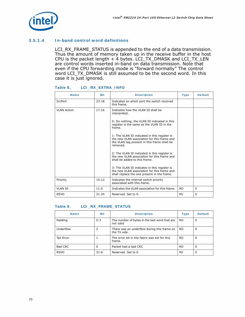
Intel® FM2224 24-Port 10G Ethernet L2 Switch Chip Data Sheet
70
3.5.1.4 In-band control word definitions
LCI_RX_FRAME_STATUS is appended to the end of a data transmission. Thus the amount of memory taken up in the receive buffer in the host CPU is the packet length + 4 bytes. LCI_TX_DMASK and LCI_TX_LEN are control words inserted in-band on data transmission. Note that even if the CPU forwarding mode is “forward normally” The control word LCI_TX_DMASK is still assumed to be the second word. In this case it is just ignored.
Table 8. LCI_RX_EXTRA_INFO
Name Bit Description Type Default
SrcPort 23:18 Indicates on which port the switch received this frame.
VLAN Action 17:16 Indicates how the VLAN ID shall be interpreted.
0: Do nothing, the VLAN ID indicated in this register is the same as the VLAN ID in the frame.
1: The VLAN ID indicated in this register is the new VLAN association for this frame and the VLAN tag present in this frame shall be removed.
2: The VLAN ID indicated in this register is the new VLAN association for this frame and shall be added to this frame.
3: The VLAN ID indicates in this register is the new VLAN association for this frame and shall replace the one present in the frame.
Priority 15:12 Indicates the internal switch priority associated with this frame.
VLAN ID 11:0 Indicates the VLAN association for this frame. RO 0
RSVD 31:24 Reserved. Set to 0. RV 0
Table 9. LCI_RX_FRAME_STATUS
Name Bit Description Type Default
Padding 5:3 The number of bytes in the last word that are not valid
RO 0
Underflow 2 There was an underflow during this frame on the TX side.
RO 0
Tail Error 1 The error bit in the fabric was set for this frame.
RO 0
Bad CRC 0 Packet had a bad CRC RO 0
RSVD 31:6 Reserved. Set to 0. RV 0

71
Intel® FM2224 24-Port 10G Ethernet L2 Switch Chip Data Sheet
3.5.1.5 Switching Modes
Frames may be transmitted in either of two modes
Directed Mode• The frame is sent to the output ports without any applied policies.
— No VLAN, security, spanning tree, or trigger checks. — This is a physical port, there is no canonical port resolution.— The switch may discard these frames for congestion management
• Source addresses are not learned. • The LCI may overwrite the CRC field with a correct CRC.• There is no VLAN tagging or stripping.
Lookup Mode• Frame is transmitted as an ordinary packet. The CPU is indistinguishable from any
other station on the network.• The LCI may overwrite the CRC field with a correct CRC.
3.5.1.6 Data Integrity
The LCI has CRC generation capability. This is purely a convenience for the CPU.
Table 10. LCI_TX_LEN
Name Bit Description Type Default
Switch Mode 31 x0 – Lookup mode – The switch uses the resources of the packet processor to forward the packet, behaving as an ordinary port, and subject to all policy checks of an ordinary port.x1 – Directed mode - The Dmask of LCI_TX_DMASK is used to specify the output port. The switch does not learn or check source addresses in this mode. A frame forwarded in this mode should never be discarded as a reason of policy. Though it is ok to discard this frame for congestion management.
RW 0
Packet Length 15:0 Length of the packet to be transmitted. Includes length of CRC even if the switch is adding the CRC.
RW 0
RSVD 30:16 Reserved. Set to 0. RV 0
Table 11. LCI_TX_DMASK
Name Bit Description Type Default
Dmask 24:1 Destination bit mask of the packet to be transmitted. If any bit of the DMASK is set, then the frame is forwarded in directed mode. If the DMASK=0 then the frame is forwarded in lookup mode.
RW 0
RSVD 31:25; 0 Reserved. Set to 0. RV 0

Intel® FM2224 24-Port 10G Ethernet L2 Switch Chip Data Sheet
72
• If the CRC is enabled then packets transferred from the CPU to the switch do not require a valid CRC. In this case the last four bytes are overwritten with a valid CRC (note: the packet data transmission must include space for the CRC).
• If CRC generation is not enabled, then it is a requirement of software to generate a valid CRC.
• The CRC is not used to check data integrity in the transmission from CPU to the switch. There is a parity check in the CPU Interface for transmission from the CPU to the switch.
3.5.2 Bootstrap Finite State Machine
Described in registers Table 36
The BOOT FSM is normally the initial chip manager.
If the AUTOBOOT signal is asserted, then the BOOT FSM starts automatically after RESET is de-asserted, initializing the chip according to the content of fusebox and returning control to the CPU Interface after the initialization is completed.
If the AUTOBOOT signal is de-asserted, then the BOOT FSM will only start if the CPU forces it to start. The CPU in this case will indicate which phases shall be executed. It is not possible to change order, it is only possible to either execute one phase or skip over that phase. Starting the BOOT FSM and defining which phase is executed is controlled by the CHIP_MODE register.
The BOOT FSM can go through 3 phases: FUSEBOX processing, RAM initialization, EEPROM processing.
3.5.2.1 Boot Phase 1 - Fusebox
During this phase, the BOOT FSM read the fusebox and stores the value read into the FUSEBOX CSRs.
3.5.2.2 Boot Phase 2 - Memory initialization
During this phase, the BOOT FSM initializes the memory to default values and also initializes the list of pointers in the scheduler.
3.5.2.3 Boot Phase 3 - EEPROM read
EEPROM operations will be started if the EEPROM_ENABLED pin-strap is set.
The SPI FSM will issue one read command to address 24'd0 - the EEPROM will continue to auto-increment through all of its memory. . The BOOT FSM will be able to stall the SPI FSM in -order to give time to any required fusebox operations.

73
Intel® FM2224 24-Port 10G Ethernet L2 Switch Chip Data Sheet
3.5.2.4 Chip Bring-up without EEPROM
STEP 1: Taking management out of reset• Deassert reset (note that both CHIP_RESET_N and EBI_RESET_N can be tied
together)• Write 0xD04 into CHIP_MODE• Poll BOOT_STATUS periodically until it goes to 0 (will be within few seconds)• You can now read/write into any management register (read
VITAL_PRODUCT_DATA as an example).
STEP 2: Programming PLL for Frame Processor• Setup PLL_FH_CTRL as desired (depends on FH_REF_CLK value)• Poll PLL_FH_STATUS to check it locks, it will normally locks in few microseconds
STEP 3: Enabling Frame Processor• Write 0 into SOFT_RESET• You can now read/write into any management register
STEP 4: Enabling Ports• Setup correct reference clock for each port using PORT_CLK_SEL (writing 0 in this
register will set all ports to use refclk A)• Take individual ports out of reset using PORT_RESET (writing 0 will take all ports
out of reset).• Bring-up the serdes as needed. The basic procedure is as follows:
— Read DS in PCS_CFG_1 (bits 30:29) to determine if port is in 1-lane or 4-lane mode. If the latter, all four lanes must be powered up. If the former, only lanes 0 and 3 need be powered up since only these lanes can serve as the single lane in 1-lane mode. Power up the lanes by writing zeros to the appropriate bits in the range 15:12 (one bit per lane) of SERDES_CTRL_2[1..24]).
— Take the serdes PLLs out of reset by writing zeros to bits 17:16 of SERDES_CTRL_2[1..24].
— Take all four lanes out of reset by writing zeros to bits 11:8 of SERDES_CTRL_2[1..24].
3.5.2.5 Management Bus
The Management bus is used to read / write registers. Access to the management bus is granted with the following precedence.
• BOOT FSM• JTAG• CPU Interface
3.5.2.6 Scan Chains Converter
The Scan Chain Converter is a management feature that converts management requests into DFT scan chain requests to grant scan access to the device from the CPU.

Intel® FM2224 24-Port 10G Ethernet L2 Switch Chip Data Sheet
74
The scan chains are used to check the DFT state of the FM2000. Access to the scan chains are granted with the following precedence:
• External SCAN IF• JTAG• Management (CPU Interface or BOOT FSM)
3.5.3 CPU Interface
Described in registers Table 47
The CPU interface in the FM2224 is a 24-bit address, 32-bit data bus used to access the registers, tables, and frames. The interface uses a handshaking protocol to allow a variable amount of delay to respond to requests. It supports off-chip DMA functionality.
3.5.3.1 General Description
• Slave-terminated protocol that allows a variable amount of delay to respond to requests
• 32-bit data interface, supporting single, Big Endian, read/write transactions• Supports parity checking on the data bus• Interrupt generation• Support for off-chip DMA PCI bridge devices.• Maximum frequency range of 66MHz• Throughput
— Reads at 528 Mb/s— Writes at 1056 Mb/s
3.5.3.2 IO requirements
• IO power supply = 3.3v • VIH min = 2v, VIL max = 0.8v.• TTL compatibility
3.5.3.3 Register Read/Write Operations
Reads and writes always act on a 32-bit word in the FM2224. Every bus request will always return a response, even if the request was to an unsupported address.
Table 12. CPU Interface External IO Description
Signal Name Direction Description
ADDR[23:2] In Address, word aligned
RW_N In Read/Write select
DATA[31:0] In / Out Data
PAR[3:0] In / Out Data parity per byte
AS_N In Address Strobe

75
Intel® FM2224 24-Port 10G Ethernet L2 Switch Chip Data Sheet
3.5.3.4 CPU interface Operation
The CPU Interface timing diagram is shown in . All input signals and all output signals are driven (or tri-stated) at the rising edge of CLK.
There are two main control signals - one to qualify the incoming request (AS_N) and the other to qualify the completion of the request (DTACK_N). There are no timing requirements from the start to the completion of a request. A write will always complete its request on the next cycle following a write request.
Figure 24. CPU Bus Interface State Diagram
CPU Interface address space
CS_N In Chip Select
DTACK_N Out Data Acknowledge
DERR Out Data Error
INTR_N Out Interrupt
CPU_RESET_N In Reset
Table 12. CPU Interface External IO Description (Continued)

Intel® FM2224 24-Port 10G Ethernet L2 Switch Chip Data Sheet
76
The Chip-Level address space 0x00000-0x000FF is for the CPU Interface. There are no physical registers within it but if a read to this address range occurs then 31'd0,CPUI_STALL will be returned. CPUI_STALL indicates whether the CPU Interface is being told to STALL (ie - the BOOT or JTAG are currently using the management bus).
The bus timing interface for read and writes are shown in next two figures. The minimum read frequency is 3 cycles and 2 for writes.
Figure 25. CPU Interface Read Cycles
Figure 26. CPU Interface Write Cycles
Table 13. CPU Interface Address Space
Address Range Module Usage
0x00000-0x000FF CPU Mgmt There are no physical registers within this module. If a read to this address range occurs then 31'd0,CPUI _STALL will be returned. CPUI_STALL indicates whether the CPU Interface is being told to STALL (ie - the BOOT or JTAG are currently using the management bus).
A write will be ignored.
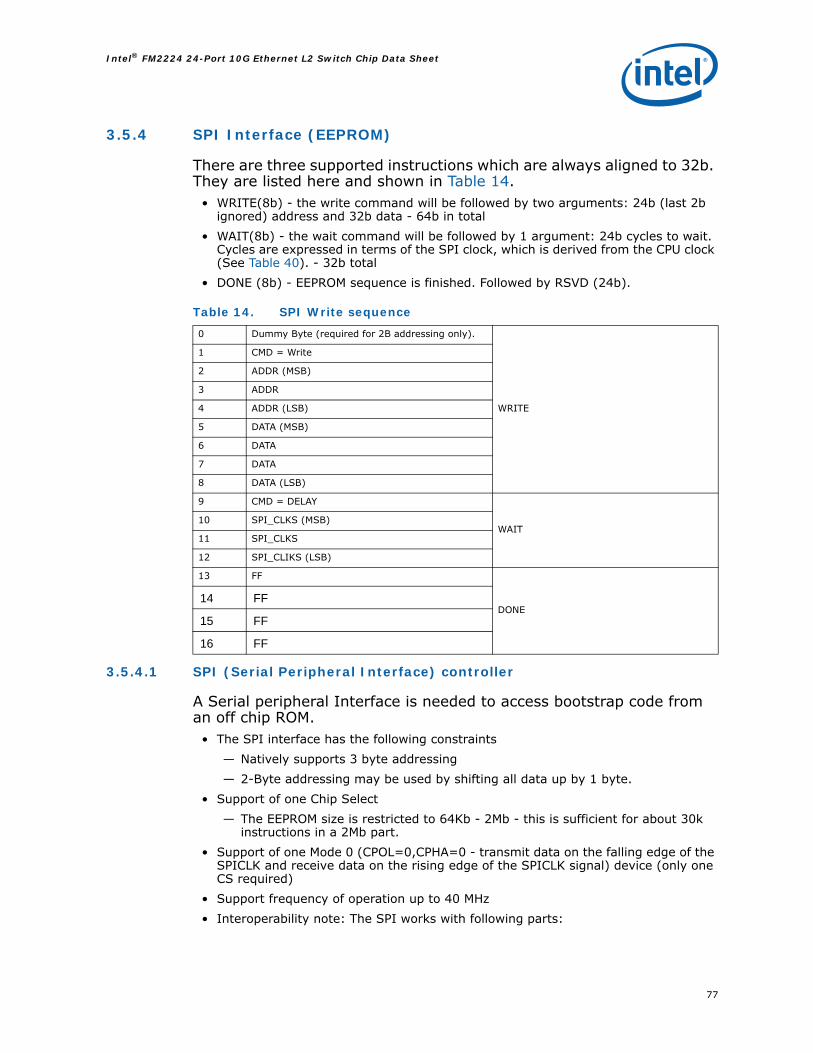
77
Intel® FM2224 24-Port 10G Ethernet L2 Switch Chip Data Sheet
3.5.4 SPI Interface (EEPROM)
There are three supported instructions which are always aligned to 32b. They are listed here and shown in Table 14.
• WRITE(8b) - the write command will be followed by two arguments: 24b (last 2b ignored) address and 32b data - 64b in total
• WAIT(8b) - the wait command will be followed by 1 argument: 24b cycles to wait. Cycles are expressed in terms of the SPI clock, which is derived from the CPU clock (See Table 40). - 32b total
• DONE (8b) - EEPROM sequence is finished. Followed by RSVD (24b).
3.5.4.1 SPI (Serial Peripheral Interface) controller
A Serial peripheral Interface is needed to access bootstrap code from an off chip ROM.
• The SPI interface has the following constraints— Natively supports 3 byte addressing — 2-Byte addressing may be used by shifting all data up by 1 byte.
• Support of one Chip Select — The EEPROM size is restricted to 64Kb - 2Mb - this is sufficient for about 30k
instructions in a 2Mb part. • Support of one Mode 0 (CPOL=0,CPHA=0 - transmit data on the falling edge of the
SPICLK and receive data on the rising edge of the SPICLK signal) device (only one CS required)
• Support frequency of operation up to 40 MHz• Interoperability note: The SPI works with following parts:
Table 14. SPI Write sequence
0 Dummy Byte (required for 2B addressing only).
WRITE
1 CMD = Write
2 ADDR (MSB)
3 ADDR
4 ADDR (LSB)
5 DATA (MSB)
6 DATA
7 DATA
8 DATA (LSB)
9 CMD = DELAY
WAIT10 SPI_CLKS (MSB)
11 SPI_CLKS
12 SPI_CLIKS (LSB)
13 FF
DONE14 FF
15 FF
16 FF

Intel® FM2224 24-Port 10G Ethernet L2 Switch Chip Data Sheet
78
— ST FLASH and EEPROM— ATMEL FLASH— Fairchild EEPROM— AKM EEPROM— MicroChip EEPROM
A SPI transaction is shown in Figure 27 and described below:• Activate SPI_CS_N and assert first data bit• On the negative edge the clock, send the following bit stream - MSB first
— Send instruction - 8'h3 (I[7:0])— Send 3 bytes of address (A[23:0])
• On the positive edge of the clock, receive each bit of data. This will continue until BOOT FSM asserts
• De-activate SPI_CS_N, Tri-state SPI_SO.
Figure 27. SPI Timing Diagram
3.5.5 LED Interface
The LED interface consists of 4 signals, CLK, DATA0, DATA1, DATA2, and ENABLE, which transmits 3 bits of status data for the LED per port over the time multiplexed data pins. The 3 bits of status of ports 0-8 are placed onto Data0 and the 3 bits of status on ports 9-16 are placed onto Data1 and the 3 bits of status of ports 17-24 are placed onto Data2.
There are two modes of operation.
Mode=0: This mode selects operations compatible to devices such as a CPLD LED display drive device. Data polarity is non-inverted.
Table 15. SPI External Interface Pin List
Signal name Signal direction Signal description
SPI_SO OUT Serial Data Output (MOSI, Master-Out- Slave-In, since FM2224 is master). Connect to EEPROM serial data input
SPI_CS_N OUT SPI Chip Select (Active Low)
SPI_SCK OUT CLOCK for SPI interafce.
SPI_SI IN Serial Data Input (MISO, Master-In-Slave-Out, since FM2224 is master). Connect to EEPROM serial data output.
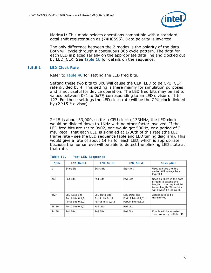
79
Intel® FM2224 24-Port 10G Ethernet L2 Switch Chip Data Sheet
Mode=1: This mode selects operations compatible with a standard octal shift register such as (74HC595). Data polarity is inverted.
The only difference between the 2 modes is the polarity of the data. Both will cycle through a continuous 36b cycle pattern. The data for each LED is placed serially on the appropriate data line and clocked out by LED_CLK. See Table 16 for details on the sequence.
3.5.5.1 LED Clock Rate
Refer to Table 40 for setting the LED freq bits.
Setting these two bits to 0x0 will cause the CLK_LED to be CPU_CLK rate divided by 4. This setting is there mainly for simulation purposes and is not useful for device operation. The LED freq bits may be set to values between 0x1 to 0x7F, corresponding to an LED divisor of 1 to 127. For those settings the LED clock rate will be the CPU clock divided by (2^15 * divisor).
2^15 is about 33,000, so for a CPU clock of 33MHz, the LED clock would be divided down to 1KHz with no other factor involved. If the LED freq bits are set to 0x02, one would get 500Hz, or a period of 2 ms. Recall that each LED is signaled at 1/36th of this rate (the LED frame rate - see the LED sequence table and LED timing diagram). This would give a rate of about 14 Hz for each LED, which is appropriate because the human eye will be able to detect the blinking LED state at that rate.
Table 16. Port LED Sequence
Cycle LED_Data0 LED_Data1 LED_Data2 Description
1 Start Bit Start Bit Start Bit Used to start the 48b series. Will always be a logical 1
2:3 Pad Bits Pad Bits Pad Bits Used as fillers in the data stream to extend the length to the required 36b frame length. These bits will always be logical 0.
4:27 LED Data BitsPort1 bits 0,1,2 …Port8 bits 0,1,2
LED Data BitsPort9 bits 0,1,2 …Port16 bits 0,1,2
LED Data BitsPort17 bits 0,1,2 …Port24 bits 0,1,2
Actual data to be transmitted
28:30 Port0 bits 0,1,2 Pad bits Pad bits
34:36 Pad Bits Pad Bits Pad Bits Enable will be asserted synchronously with bit 36

Intel® FM2224 24-Port 10G Ethernet L2 Switch Chip Data Sheet
80
Figure 28. Serial LED Timing Diagram
Below is the encoding of the 3 bits per port:• Port LED0 (Red)
— Off - Port has no link synch or remote fault error— On - Port has a link synch error or no signal— Blinking - Port has a remote fault
• RX LED1 (Green)—Off - Port is not enabled—On - Port has link and is enabled—Blinking - Port is receiving data (rate will be controllable by a programmable decimated clock and fixed hysteresis value which when latches indicates that traffic has been received)
• TX LED2 (Green)— Off - Port is not transmitting data— Blinking - Port is transmitting data (rate will be controllable by a programmable
decimated clock and some fixed hysteresis value which when latches indicates that traffic has been transmitted.
This interface clock is a multiple of CLK_CPUI and CLK_LED.
3.5.6 TAG
The JTAG controller is compliant to the IEEE 1149.1-2001 specification. The JTAG provides basic external chip debug features,
• Access to an identification register.• Access to the boundary scan.• Access to the internal scan chains.• Ability to Clamp and HighZ all outputs (except SerDes).
The maximum frequency of operation is 40MHZ.
The Supported operations of these registers are:• Load IR (instruction register) • Capture - initializes/captures/freezes value of register

81
Intel® FM2224 24-Port 10G Ethernet L2 Switch Chip Data Sheet
• Shift - serially shifts in/out value into/out of register.• Update - validates the contents of the register. Ie. Logic can now use the new value
for its internal operation.
The JTAG reset domain is separate and independent from the chip reset domain.
3.5.6.1 Tap Controller
The tap controller is a finite state machine of 16 states controlled by the 5 pin JTAG interface. It is defined by IEEE 1149.1-2001.
3.5.6.2 Instruction Register
Supported JTAG Instructions
3.5.6.3 Bypass Register
The bypass register is a 1 bit register that connects between TDI and TDO. When the bypass register is selected by the instruction, the data driven on the TDI input pin is shifted out the TDO interface one cycle later.
3.5.6.4 TAG Scan Chain
The boundary scan register is a 162-bit deep shift register. Refer to the BSDL description file for pin assignment.
Table 17. Supported JTAG Instructions
Instruction Code (6b) Description
IDCODE x01 Selects the identification register.
SAMPLE/PRELOAD x02 Select the boundary scan register. Sample input pins to input boundary scan register, preload the output boundary scan register.
EXTEST x03 Select the boundary scan register. Output boundary scan register cells drive the covered output pins. Input boundary cell registers sample the input pins.
HIGHZ x06 Selects the bypass register and sets all covered output pins to high impedance.
CLAMP x07 Forces a known value on the outputs, but uses the bypass register to shorten scan length.
BYPASS x3F Selects the bypass register.
Table 18. JTAG ID Register
Bit Description Value
31:28 Silicon Version Number 0x00 (pre-A5)
0x01 (A5 and later)
27:12 Manufacturer part number 0xae18
1:11 Manufacturer ID 0x215
0 Mandatory JTAG field b1

Intel® FM2224 24-Port 10G Ethernet L2 Switch Chip Data Sheet
82
3.6 Clocks
3.6.1 SerDes Clocks, RCK[A:B][1:4]P/N
The SerDes reference clocks are externally provided, low jitter, differential CMOS/CML clocks in the range of 100MHz to 400MHz, representing 1/10th the serial data rate. The requirements for these inputs are given in Table 19.
Notes: 1. UI refers to the Bit Time period
2. RCUI refers to the Reference Clock period
3.6.2 CPU Interface Clock
The clock source for the CPU interface on the FM2224 must meet the following requirements:
• 3.3V CMOS drive• Maximum frequency of 100 MHz.
3.6.3 JTAG Clock
The FM2224 supports JTAG. The clock source must meet the LVTTL specification and:
• Duty cycle distortion of 40/60%, maximum • Maximum frequency of 40 MHz
3.6.4 Frame Handler Clock
The frame handler clock controls the rate at which frame headers are processed in the frame handler block. Frame headers are processed one header per clock cycle, so if the aggregated 24-port frame throughput is desired to be 300 million frames per second, the frame handler clock must be set at 300 MHz. The aggregate frame rate for all ports in frames per second (FPS) should never exceed the frame handler clock speed in Herz (The aggregate frame rate for all ports in frames per second (FPS) should never exceed the frame handler clock
Table 19. Reference Clock Requirements
Symbol Description Min Typ Max Units
VIL-RC Low-level CML/CMOS input voltage 0 VDD-0.5 V
VIH-RC High-level CML/CMOS input voltage 0 VDD V
Clock frequency range 100 400 MHz
Duty cycle 40 50 60 %
Skew between + and – inputs of a single reference clock
.05 RCUI
JCLK-REF Input jitter (peak to peak) 0.1 UI1
TRRef, TFRef Rise/Fall time of differential inputs 0.2 0.25 RCUI2

83
Intel® FM2224 24-Port 10G Ethernet L2 Switch Chip Data Sheet
speed in Megaherz (MHz) or unpredicted behavior will result Hz) or unpredicted behavior will result. The frame handler clock is generated by an internal PLL using the FH_PLL_REFCLK clock input pin as its input. The relationship between the input frequency and the PLL output frequency to the frame handler is controlled by parameters input in the PLL_FH_CTRL register (See Table 43). A simplified schematic of the PLL circuit is shown that will clarify the meaning of the input parameters.
Figure 29. Frame Handler Clock Generation
The resulting equation governing the PLL output is:
PLL_OUT = FH_PLL_REFCLK x M/NP
Where:• N ==> 1 to 16• M ==> 4 to 128• 150 MHz < FVCO (point A) < 650 MHz• 12.5 MHz < PLL output < 360 MHz• 1.2 MHz < FH_PLL_REFCLK < 70 MHz
Note: See Table 44 for examples of N, M, and P settings.

Intel® FM2224 24-Port 10G Ethernet L2 Switch Chip Data Sheet
84
4.0 Electrical Specifications
The following tables provide recommended operating conditions for the FM2224:
4.1 Absolute Maximum Ratings
4.2 Recommended Operating Conditions
(1) Operation at VDD = 1.25V may be desired for provisioning purposes. See Note on VDD supply voltage below for details.
Table 20. Absolute Maximum Ratings
Parameter Symbol Min Max Units
Core Voltage VDD -0.3 2 Volts
SerDes Supply Voltage VDDX -0.3 2 Volts
SerDes Bias Voltage VDDA -0.3 2 Volts
Transmitter Termination Voltage VTT -0.3 2 Volts
LVTTL Power Supply VDD33 -0.3 3.9 Volts
PLL Analog power supply VDDA33 -0.3 3.9 Volts
Case Temp under bias - +130 °C
Storage Temp -65 +150 °C
ESD -2000 +2000 Volts
Table 21. Recommended Operating Conditions
Parameter Symbol Min Typ Max Units
Core Voltage VDD 1.14 1.2 1.26 Volts
1.19 1.25 1.31 Volts1
SerDes Supply Voltage VDDX 1.14 1.2 1.26 Volts2,4
0.95 1.0 1.1 Volts3,4
SerDes Bias Voltage VDDA 1.14 1.2 1.26 Volts
0.95 1.0 1.1 Volts
LVTTL Power Supply VDD33 3.14 3.3 3.47 Volts
PLL Analog power supply VDDA33 3.14 3.3 3.47 Volts
Transmitter Termination Voltage VTT Vdd 1.5 1.8 Volts
Operating Temp (Case)
Commercial 0 +85 °C
Extended 0 +105 °C
Industrial -40 +115 °C

85
Intel® FM2224 24-Port 10G Ethernet L2 Switch Chip Data Sheet
(2) Connect a 1.2KΩ resistor from RREF to VDDX for 1.2V operation.
(3) Connect a 1.0KΩ resistor from RREF to VDDX for 1.0V operation.
(4) Operating with VDDX = 1.0V results in less power dissipation, but operating with VDDX =1.2V may be desired to avoid implementation of another supply voltage. Use caution if doing this as the proper filtering must be implemented. See the Design Guide and/or contact Intel® for details.
Note on VDD supply voltage:
In accordance with IEEE 802.3ae, each 10G interface can experience a maximum frame rate of 14,880,952 frames per second (fps). That frame rate results from a 10 gigabit per second data rate consisting of a steady stream of minimum size frames (64B) with minimum spacing (20B) between each. The 20B spacing is the sum of the 7B preamble plus 1B SFD plus 12B minimum interframe gap. Although it is an unusual case, the FM2224 can process frames with this frame rate on all ports simultaneously, an aggregate frame throughput of 357 million frames per second (Mfps). In other words, the FM2224 is fully provisioned. If this frame rate is expected however, a nominal VDD of 1.25V should be used and the actual voltage must be kept above a value that is dependent on the maximum operating case temperature of the device, TCASE.
Figure 30. Frame Rate vs VDD and Case Temperature.

Intel® FM2224 24-Port 10G Ethernet L2 Switch Chip Data Sheet
86
As shown in the figure, each line is a boundary where the FM2224 is provisioned for the given aggregate frame rate for all points above that line.
To calculate the maximum frame rate for use conditions in which not all 24 ports are operated, or not all operated at 10G rates, the following table may be useful.
For example, with 20 ports operating at 10 Gbps and 4 ports operating at 1 Gbps, the maximum possible aggregate frame rate is 303.6 Mfps. This frame rate is provisioned for an Industrial grade part (115ºC maximum case temperature) even if a 1.2V +/- 5% VDD supply voltage is used. As a second example, using only 23 ports, all in 10 Gbps mode results in a worst case aggregate frame rate of 342 Mfps. Keeping VDD above approximately 1.18V will ensure that a Commercial grade part (85ºC maximum case temperature) is fully provisioned for the worst case frame rate.
Port Speed Maximum Frame Rate (Mfps)
1 Gbps 1.488
2.5 Gbps 3.72
10 Gbps 14.88
Table 22. DC Characteristics of 4mA LVTTL Outputs
Parameter Symbol Test Conditions Min Typ Max Units
HIGH Force Tri-State output leakage
IOZH VDD= Max Vo=VDD -1 - +1 µA
LOW Force Tri-State output leakage
IOZL VDD=Max Vo=GND -1 - +1 µA
Output HIGH Current IODH VDD=1.2V, VDD33=3.3 V, VO = 1.5
- -17 - mA
Output LOW Current IODL VDD=1.2 V, VDD33=3.3 V, VO = 1.5 V
- 20 - mA
Output HIGH Voltage VOH VDD= Min VDD33=Min IOH= -0.4 mA
VDD33 - 0.2
- - V
Output HIGH Voltage VOH VDD= Min VDD33=Min IOH= -4.0 mA
VDD33 - 0.5
- - V
Output LOW Voltage VOL VDD= Min VDD33=Min IOL= -0.4 mA
- - 0.2 V
Output LOW Voltage VOL VDD= Min VDD33=Min IOL= -4.0 mA
- 0.2 0.4 V
Short Circuit Current IOS VDD=MAX Vo=GND -32 mA
Power Supply Quiescent Current
IAA VDD= Max VDD33=Max
74 µA
Power Supply Quiescent Current
IAA Tri-stated -1 µA

87
Intel® FM2224 24-Port 10G Ethernet L2 Switch Chip Data Sheet
Table 23. DC Characteristics of 8mA LVTTL Outputs
Parameter Symbol Test Conditions Min Typical Max Units
HIGH Force Tri-State output leakage
IOZH VDD= Max Vo=VDD -1 - +1 µA
LOW Force Tri-State output leakage
IOZL VDD=Max Vo=GND -1 - +1 µA
Output HIGH Current IODH VDD=1.2 V, VDD33=3.3 V, VO = 1.5 V
- -35 - mA
Output LOW Current IODL VDD=1.2 V, VDD33=3.3 V, VO = 1.5 V
- -40 - mA
Output HIGH Voltage VOH VDD= Min VDD33=Min IOH= -0.4 mA
VDD33 - 0.2
- - V
Output HIGH Voltage VOH VDD= Min VDD33=Min IOH= -4.0 mA
VDD33 - 0.5
- - V
Output LOW Voltage VOL VDD= Min VDD33=Min IOL= -0.4 mA
- - 0.2 V
Output LOW Voltage VOL VDD= Min VDD33=Min IOL= -4.0 mA
- 0.2 0.4 V
Short Circuit Current IOS VDD=MAX Vo=GND -64 mA
Power Supply Quiescent Current
IAA VDD= Max VDD33=Max
74 µA
Power Supply Quiescent Current
IAA Tri-stated -1 µA
Table 24. DC Characteristics of LVTTL Inputs
Parameter Symbol Test Conditions Min Typical Max Units
Input HIGH Level (Input and I/O pins)
VIH Guaranteed Logic HIGH Level
2 - VDD33 +0.5(1)
V
Input LOW Level (Input and I/O pins)
VIL Guaranteed Logic LOW Level
-0.3 - 0.8 V
Input Hysterisis VH it0 5 mV
Input Hysterisis VH it2 200 mV
Input HIGH Current (Input pins)
IIH VDD=Max, VI=VIH(Max)
+-1 µA
Input HIGH Current (I/O pins) IIH VDD=Max, VI=VCC +-1 µA
Input LOW Current (Input pins) IIL VDD=Max, VI=GND +-1 µA
Input LOW Current (I/O pins) IIL VDD=Max, VI=GND +-1 µA
Clamp Diode Voltage VIK VDD=Min, IIN=-18mA
-0.7 -1.2 V
Quiescent Power Supply Current
IDD33L VDD=Max, VCC=Max, VIN=GND
0.1 10 µA
Quiescent Power Supply Current
IDD33H VDD=Max, VCC=Max, VIN=VDD
0.1 10 µA

Intel® FM2224 24-Port 10G Ethernet L2 Switch Chip Data Sheet
88
Note: Restrict total input voltage, including overshoot, to 4.5V maximum.
4.3 AC Timing Specifications
a. HiDrv bit set to 0, LoDrv bit set to 1 in SERDES_CNTL_2 register - see Table 132, and Current Drive bits set to 1100 in SERDES_CNTL_1 register - see Table 130.
b. VTT = 1.8V, HiDrv bit set to 1, LoDrv bit set to 0 in SERDES_CNTL_2 register - see Table 132, and Current Drive bits set to 0011 in SERDES_CNTL_1 register - see Table 130.
c. AC coupled operation only
d. Based on CJPAT.
e. 20% to 80%.
Table 25. XAUI Transmitter Characteristics
Symbol Parameter Min Typ Max Units
VSW Output voltage (peak-to-peak, single-ended)
200a 500 750 b mV
VDIFF-PP Output voltage (peak-to-peak, differential) 400 a 1000 1500 b mV
VOL Low-level output voltage Vtt-1.5* VSW
VOH High-level output voltage Vtt-0.5* VSW
VTCM Transmit common-mode voltagec Vtt-VSW
[email protected] Gb/S
Transmitter Total Jitter (Peak-Peak)d .24 UI
Random jitter component (RJ) .12
Deterministic jitter component (DJ) .12
[email protected] Gb/S
Transmitter Total Jitter (Peak-Peak)d .35 UI
Random jitter component (RJ) .18
Deterministic jitter component (DJ) .17
ZOSE Single Ended Output Impedance 40 50 60 Ohms
ZD Differential Output Impedance 80 100 120 Ohms
TTR, TTF Rise, fall times of differential outputse 80 110 ps
Table 26. XAUI Receiver Characteristics
Symbol Parameter Min Typ Max Units
VLOS Low signal differential input threshold voltage 85 mV
VIN Differential input voltage, peak to peak 170 2000 mV
VRCM Common mode voltage 0.70 V
TRR, TRF Rise, fall times of differential inputs 160 ps

89
Intel® FM2224 24-Port 10G Ethernet L2 Switch Chip Data Sheet
a. CJPAT
b. Frequency range of 100MHz to 1.875GHz
c. Without damage to any signal pin
4.3.1 CPU Interface, General Timing Requirements
Figure 31. CPU Signal Timing
JRT @ 1.25 Gbps
Total jitter tolerancea .71 UI
Random jitter component (RJ) .26
Deterministic jitter component (DJ) .45
JTT@ 3.25 Gbps
Total jitter tolerancea .65 UI
Random jitter component (RJ) .24
Deterministic jitter component (DJ) .41
ZIN Impedance, single-ended 40 50 60 W
LDR Differential return lossb 10 dB
VRHP Hot plug voltage (applied with power on or off)c
-.5 1.6 V
Table 26. XAUI Receiver Characteristics (Continued)

Intel® FM2224 24-Port 10G Ethernet L2 Switch Chip Data Sheet
90
4.3.2 JTAG Interface
The JTAG interface follows standard timing as defined in the IEEE 1149.1 Standard Test Access Port and Boundary-Scan Architecture, 2001.
Note: When not using the JTAG interface, either drive the TCK pin with an external clock, or drive the TRST_N pin low. Conversely, when using the JTAG interface assert TRST_N along with chip reset to ensure proper reset of the JTAG interface prior to use.
Table 27. CPU Interface Timing Constraints
Parameter Symbol Min Typ Max Units TestConditions
Setup time for CS_N, AS_N, DS_N and RW_N, to rising edge of clock
Tsu1 3.0 - - ns -
Hold time for CS_N, AS_N and RW_N, to rising edge of clock
Th1 0.5 - - ns -
Setup time for ADDR and DATA(in) to rising edge of clock
Tsu2 3.0 - - ns -
Hold time for ADDR and DATA(in) to rising edge of clock
Th2 0.5 - - ns -
Output valid for DTACK_N and DATA(out) to rising edge of clock
Tov 0 - 4.5 ns
Notes• DTACK_INV, RW_N_INV, SYNC_MODE are static signals. They must be stable before RESET_N is de-
asserted.• CS_N must stay active from before the assertion of AS_N to DTACK_N being de-asserted. The minimum
setup time before AS_N is 200pS.• A minimum of one idle cycle is required between successive transactions to different slave devices.• BUSIF_RESET and INTR are asynchronous signals. • Typical latency to access an internal 32-bit register is in the range of 100-150ns.

91
Intel® FM2224 24-Port 10G Ethernet L2 Switch Chip Data Sheet
5.0 Register Definitions
This section provides information on the registers used in the FM2224. Although the registers are generally directly accessible, it is recommended that they be accessed through the Intel® API where related registers can be rationally configured as a group in the context of the application.
5.1 Register Conventions
Registers follow these conventions:• All registers are 32 bits in length• Tables may be more than 32 bits in length• There are four types of register fields:
— RW - Read / Write— RO - Read Only— CR - Clear on Read— PIN - Pin
• Registers are located on different reset domains and are reset to their default value only when their respective domain is reset. The reset domains are:— Global Reset Domain: Reset only when CHIP_RESET_N is asserted— Ethernet Port Logic Reset Domain: Reset when CHIP_RESET_N is asserted or
the port reset is active (see PORT_RESET register)— Frame Handler Reset Domain: Reset when frame handler reset is asserted (see
SOFT_RESET register)
Note: The entries in the MAC address (MA), VLAN Information Database (VID), Forwarding Information Database (FID), and Management Information Base (MIB) tables are larger than 32 bits, as follows: MA: 95 bits; VID: 64 bits; FID: 50 bits; MIB: 64 bits. The FM2000 supports atomic access to these addresses. A read or write to the MAC address, VLAN, or Flooding ID tables, or the read of a MIB counter is atomic.
5.2 Register Map
Note: The statistics register map is detailed in section 5.7.
Table 28. Global Register List
Global Registers
Name Reset Domain Description Address
BOOT_STATUS Global Boot status 0x00000
SOFT_RESET Global Reset switch by software 0x00300
PORT_RESET Global Reset port by software 0x00318
CHIP_MODE Global Configures various chip-level modes 0x00301
CLK_MULT_1 Global Clock multiples between the CPU interface, LED interface, and SPI interface
0x00302

Intel® FM2224 24-Port 10G Ethernet L2 Switch Chip Data Sheet
92
FRAME_TIME_OUT Global Configures whether (and how) frames time out
0x00303
VPD Global Vital Product Data 0x00304
PLL_FH_CTRL Global Frame Handler PLL Control 0x00315
PLL_FH_STAT Global Frame Handler PLL Status 0x00316
PORT_CLK_SEL Global Selects between 2 CML clocks per port
0x00317
Table 29. Switch Configuration Register List
Switch Configuration Registers
Name Reset Domain Description Address
INTERRUPT_DETECT Global Detects an interrupt 0x00309
GLOBAL_EPL_INT_DETECT Global Detects an interrupt on a port 0x0030A
MGR_IP Global Chip interrupt pending 0x0030B
MGR_IM Global Chip interrupt mask 0x0030C
FRAME_CTRL_IP Global Frame control interrupt pending 0x0030D
FRAME_CTRL_IM Global Frame control interrupt mask 0x0030E
PERR_IP Global Parity error interrupt pending 0x00312
PERR_IM Global Parity error interrupt mask 0x00313
PERR_DEBUG Global Parity error debug 0x00314
TRIGGER_IP FH Trigger interrupt pending 0x640C6
TRIGGER_IM FH Trigger interrupt mask 0x640C7
PORT_MAC_SEC_IP FH MAC security interrupt pending 0x640C4
PORT_MAC_SEC_IM FH MAC security interrupt mask 0x640C5
PORT_VLAN_IP_1 FH VLAN violation interrupt pending 0x640C0
PORT_VLAN_IM_1 FH VLAN violation interrupt mask 0x640C1
PORT_VLAN_IP_2 FH VLAN violation interrupt pending 0x640C2
PORT_VLAN_IM_2 FH VLAN violation interrupt mask 0x640C3
SYS_CFG_1 General feature configuration 0x60001
SYS_CFG_2 Mgmt General feature configuration in the asynchronous logic
0x58121
SYS_CFG_3 Global Most significant bit of the CPU’s MAC address (Port 0)
0x60002
SYS_CFG_4 Global Least significant bit of the CPU’s MAC address (Port 0)
0x60003
SYS_CFG_6 Global Ether-type Trap 0x60004
SYS_CFG_7 Global Age time 0x0030F
PORT_CFG_1 [1..24] Global Security and VLAN settings 0x54000+i
PORT_CFG_2 [1..24] Global Port-based VLAN flood map 0x60060+i
HEADER_MASK [0..3] Mgmt 128-bit mask of the Ethernet header 0x581100x581110x581120x58113
Table 28. Global Register List (Continued)

93
Intel® FM2224 24-Port 10G Ethernet L2 Switch Chip Data Sheet
Table 30. Logical CPU Interface Register List
LCI Configuration Registers
Name Reset Domain Description Address
LCI_RX_FIFO Mgmt LCI RX FIFO 0x04000
LCI_TX_FIFO Mgmt LCI TX FIFO 0x04001
LCI_IP Mgmt LCI interrupt 0x04002
LCI_IM Mgmt LCI interrupt mask 0x04003
LCI_STATUS Mgmt LCI status 0x04004
LCI_CFG Mgmt LCI mode configuration 0x04005
Table 31. Bridge Register List
Bridge Registers
Name Reset Domain Description Address
MA_TABLE[0..16383] Global MAC address table 0x10000+i*4
VID_TABLE[0..4095] Global VLAN table 0x50000+i*2
FID_TABLE[0..4095] Global Spanning tree status per VLAN 0x52000+i*2
MA_TABLE_CFG Mgmt MAC address table configuration 0x58120
MA_TABLE_STATUS_1 Mgmt Status of switch-modified entries in the MAC address Table
0x58000
MA_TABLE_STATUS_2 Mgmt Bin full count and hash 0x58001
MA_TABLE_STATUS_3 Mgmt No source address lookup count 0x03010
TRUNK_PORT_MAP [1..24] FH Indicates whether a port is in a Link Aggregation Group
0x63000+i
TRUNK_GROUP_1 [0..11] FH Link Aggregation Group entries 0-5
0x63020+i
TRUNK_GROUP_2 [0..11] FH Link Aggregation Group entries 6-11
0x63040+i
TRUNK_GROUP_3 [0..11] FH Length of Link Aggregation Group 0x63060+i
TRUNK_CANONICAL [1..24] FH Mapping to canonical port 0x60020+i
TRUNK_HASH_MASK FH byte mask for link aggregation hash function
0x61000
TRIGGER_CFG [0..15] FH Configures user programmable triggers
0x62020+i
TRIGGER_PRI [0..15] FH Switch priority to be in trigger 0x62040+i
TRIGGER_RX [0..15] FH Source port of trigger 0x62060+i
TRIGGER_TX [0..15] FH Destination port of trigger 0x62080+i

Intel® FM2224 24-Port 10G Ethernet L2 Switch Chip Data Sheet
94
Table 32. Congestion Management Register List
Traffic Management Registers
Name Reset Domain Description Address
RX_PRI_MAP [0..24] FH Mapping of ingress priority to switch priority
0x60040+i
CM_PRI_MAP_1 FH Mapping 1 of switch priority to PWD priority
0x64000
CM_PRI_MAP_2 FH Mapping 2 of switch priority to PWD priority
0x64001
SCHED_PRI_MAP FH Mapping of switch priority to scheduling priority
0x60000
LFSR_CFG FH Random number configuration for PWD
0x64002
QUEUE_CFG_1 [0..24] FH RX and TX queue shared watermark for frame discard check
0x64020+i
QUEUE_CFG_2 [0..24] FH RX private watermark and configuration
0x64040+i
QUEUE_CFG_3 FH Congestion management priority watermark selection
0x65000
QUEUE_CFG_4 FH Congestion management low and high watermark
0x64003
STREAM_STATUS_1 [0..24] FH Occupancy for RX and TX queues 0x64060+i
STREAM_STATUS_2 FH Occupancy of global stream memory 0x64008
EGRESS_SCHED_1 Mgmt Egress scheduling configuration 0x02040
EGRESS_SCHED_2 Mgmt Egress scheduling weights 0x02041
GLOBAL_PAUSE_WM [0..24] FH Watermarks for PAUSE based on stream memory occupancy
0x64080+i
RX_PAUSE_WM [0..24] FH Watermarks for PAUSE based on RX queue occupancy
0x640A0+i
SAF_MATRIX[0..24] FH Cut-through switching configuration 0x650C0+i
JITTER_CFG Mgmt Configures the TX jitter controller 0x020FC
Table 33. Statistics and Counter Registers
Statistics and Counter Registers
Name Reset Domain Description Address
STATS_CFG Enable/Disable counter groups 0x66200
STATS_DROP_COUNT Counts event rate related counter drops
0x66202
GROUP 1 COUNTERS RX packet counters per type 0x70000
GROUP 2 COUNTERS RX packet counters per size 0x70080
GROUP 3 COUNTERS RX octet counters 0x700A0
GROUP 4 COUNTERS RX packet counters per priority 0x70010
GROUP 5 COUNTERS RX octet counters per priority 0x70120
GROUP 6 COUNTERS RX packet counters per flow 0x70100

95
Intel® FM2224 24-Port 10G Ethernet L2 Switch Chip Data Sheet
GROUP 7 COUNTERS TX packet counters per type 0x70020
GROUP 8 COUNTERS TX packet counters per size 0x700A8
GROUP 9 COUNTERS TX octet counters 0x802C0
GROUP 10 COUNTERS Congestion Management counters 0x66080
GROUP 11 COUNTERS VLAN octet counters 0x66180
GROUP 12 COUNTERS VLAN packet counters 0x66100
GROUP 13 COUNTERS Trigger counters 0x660C0
Table 34. Ethernet Port Logic Register List
PHY Registers(EPL register addresses are 0x8000 + 0x400*(N-1) + Offset, where N is the port number)
Name Reset Domain Description Offset
SERDES_CTRL_1 EPL Per-lane DEQ and DTX 0x000
SERDES_CTRL_2 EPL Lane, PLL, and mode control 0x001
SERDES_CTRL_3 EPL Signal detect de-assertion count 0x002
SERDES_TEST_MODE EPL BIST test modes 0x003
SERDES_STATUS [1..24] EPL Counter for any interrupt in the SERDES
0x004
SERDES_IP EPL SERDES interrupt pending 0x005
SERDES_IM EPL SERDES interrupt mask 0x006
SERDES_BIST_ERR_CNT EPL BIST error count per lane. 0x008
PCS_CFG_1 EPL PCS Control 0x009
PCS_CFG_2 EPL Data value on local TX fault 0x00A
PCS_CFG_3 EPL Data value on remote TX fault 0x00B
PCS_CFG_4 EPL Data value on signal ordered set Sent 0x00C
PCS_CFG_5 EPL Data value on signal ordered set received
0x00D
PCS_IP EPL PCS interrupt pending 0x00E
PCS_IM EPL PCS interrupt mask 0x00F
PACING_PRI_WM [0..7] EPL Watermarks per priority for inter-frame gap stretch
0x010+i
PACING_RATE EPL Pacing rate for inter-frame gap stretch 0x018
PACING_STATUS EPL Pacing status for inter-frame gap stretch
0x019
MAC_CFG_1 EPL MAC configuration 1 0x01A
MAC_CFG_2 EPL MAC configuration 2 0x01B
MAC_CFG_3 EPL MAC configuration 3: Pause time value 0x01C
MAC_CFG_4 EPL MAC Configuration 4: Pause re-send time
0x01D
MAC_CFG_5 EPL MAC configuration 5: Most significant 16 bits of the MAC address, SA for Pause
0x01E
Table 33. Statistics and Counter Registers (Continued)

Intel® FM2224 24-Port 10G Ethernet L2 Switch Chip Data Sheet
96
5.3 Global Registers
5.3.1 Global Register Tables
Note: If all steps are enabled, then this register will successively go through the following sequence: 0xF, 0x7, 0x3, 0x0.
MAC_CFG_6 EPL MAC configuration 6: Least significant 32 bits of the MAC address, SA for Pause
0x01F
TX_PRI_MAP_1 EPL Switch to egress 1 0x020
TX_PRI_MAP_2 EPL Switch to egress 2 0x021
MAC_STATUS EPL Idle status 0x022
MAC_IP EPL Interrupt pending 0x023
MAC_IM EPL Interrupt mask 0x024
EPL_INT_DETECT EPL Interrupt detect for the Ethernet Port Logic
0x02B
EPL_LED_STATUS EPL LED status bits 0x02A
STAT_EPL_ERROR1 EPL Error count 0x025
STAT_EPL_ERROR2 EPL Error count 0x028
STAT_TX_CRC EPL BAD CRC transmitted count 0x27
STAT_TX_PAUSE EPL Pause transmitted count 0x26
STAT_RX_JABBER EPL Received oversized with bad CRC 0x29
STAT_TX_BYTECOUNT EPL Transmit byte count 0x2C
Table 35. Scan Chain Access Register List
Global Registers
Name Ref Description Address
SCAN_FREQ_MULT Boot status 0x00100
SCAN_CTRL Reset switch by software 0x00101
SCAN_SEL Reset port by software 0x00102
SCAN_DATA_IN Configures various chip level modes 0x00103
SCAN_DATA_OUT Clock multiples between CPU and LED and SPI 0x00104
Table 36. BOOT_STATUS
Name Bit Description Type Default
Memory Initialization 2 Indicates that the boot FSM has not completed this step yet.
RO 0
EEPROM Reading 1 Indicates that the boot FSM has not completed this step yet.
RO 0
Boot Running 0 The boot process is actually running (1) or completed (0). The CPU shall not attempt to read/write any register until this bit is 0.
RO 0
RSVD 31:3 Reserved. Set to 0. RV 0
Table 34. Ethernet Port Logic Register List (Continued)
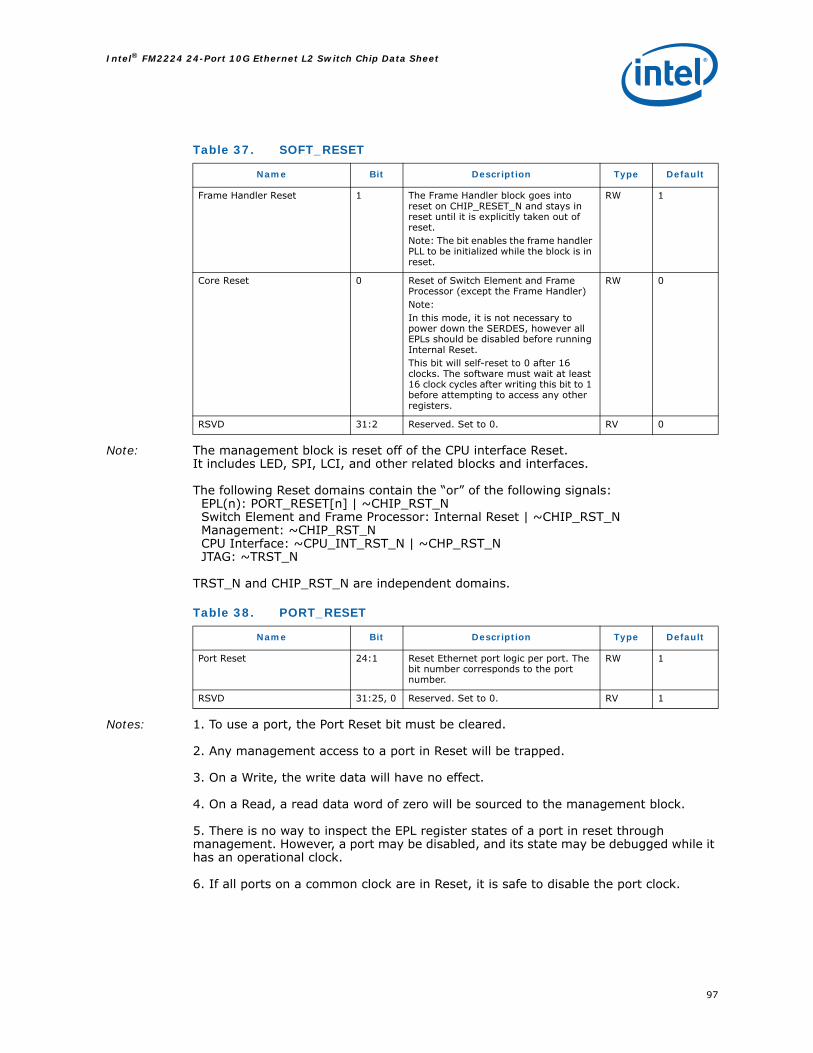
97
Intel® FM2224 24-Port 10G Ethernet L2 Switch Chip Data Sheet
Note: The management block is reset off of the CPU interface Reset.It includes LED, SPI, LCI, and other related blocks and interfaces.
The following Reset domains contain the “or” of the following signals:EPL(n): PORT_RESET[n] | ~CHIP_RST_NSwitch Element and Frame Processor: Internal Reset | ~CHIP_RST_NManagement: ~CHIP_RST_N CPU Interface: ~CPU_INT_RST_N | ~CHP_RST_NJTAG: ~TRST_N
TRST_N and CHIP_RST_N are independent domains.
Notes: 1. To use a port, the Port Reset bit must be cleared.
2. Any management access to a port in Reset will be trapped.
3. On a Write, the write data will have no effect.
4. On a Read, a read data word of zero will be sourced to the management block.
5. There is no way to inspect the EPL register states of a port in reset through management. However, a port may be disabled, and its state may be debugged while it has an operational clock.
6. If all ports on a common clock are in Reset, it is safe to disable the port clock.
Table 37. SOFT_RESET
Name Bit Description Type Default
Frame Handler Reset 1 The Frame Handler block goes into reset on CHIP_RESET_N and stays in reset until it is explicitly taken out of reset. Note: The bit enables the frame handler PLL to be initialized while the block is in reset.
RW 1
Core Reset 0 Reset of Switch Element and Frame Processor (except the Frame Handler) Note:In this mode, it is not necessary to power down the SERDES, however all EPLs should be disabled before running Internal Reset. This bit will self-reset to 0 after 16 clocks. The software must wait at least 16 clock cycles after writing this bit to 1 before attempting to access any other registers.
RW 0
RSVD 31:2 Reserved. Set to 0. RV 0
Table 38. PORT_RESET
Name Bit Description Type Default
Port Reset 24:1 Reset Ethernet port logic per port. The bit number corresponds to the port number.
RW 1
RSVD 31:25, 0 Reserved. Set to 0. RV 1

Intel® FM2224 24-Port 10G Ethernet L2 Switch Chip Data Sheet
98
Table 39. CHIP_MODE
Name Bit Description Type Default
Bypass PLL 13 Bypass the PLL in the Frame Handler and take the clock from off-chip. Note: this is not the same as the PLL_FH_CTRL[bypass] bit.This bit must be reset to 0 after the bootstrap is completed and FH PLL has been initialized and locked for the device to work properly.This bit should be held at 1 for scan test of the Frame Handler.
RW 1
Exec Mem Init 10 x1 – Execute memory initialization phase of BOOT FSM.x0 – Do not execute memory initialization phase of BOOT FSM
RW 0
Exec EEPROM 9 x1 – Execute EEPROM phase of BOOT FSM.x0 – Do not execute EEPROM phase of BOOT FSM
RW 0
Start BOOT FSM 8 x1 – Starts the BOOT FSM using the content of CHIP_MOD[9:11] to define which step is executed or skipped. This is a self clear register once the BOOT FSM has completed the operation.x0 – Do not start the BOOT FSM.
RW 0
RSVD 7:4 Reserved. Set to 0. RV 0
LED Mode 3 1 – Invert LED data on the LED interface.0 – Do not invert LED data on the LED interface.
RW 0
LED Enable 2 1 – Present LED signals on the LED interface.0 – Disable the generation of LED signals
RW 0
RSVD 1 Reserved. Set to 0. RV 0
DFT Access 0 Grants access of the DFT functions to the control interfaces
RW 0
RSVD 31:14, 12:11
Reserved. Set to 0. RV 0
Table 40. CLK_MULT_1
Name Bit Description Type Default
SPI Divider 15:8 The SPI EEPROM clock dividerSPI clock = CPU Interface clock / (2*(SPI Div+1)Default value gives CPU clock speed divisor of 52.
RW 0x19
LED Divider 7:0 LED clock divisor0x0: LED clock = CPU_CLK / 4
0x1…0x7F: LED Clock = CPU_CLK/(215 * LED Div)
RW 0x00
RSVD 31:16 Reserved. Set to 0. RV 0

99
Intel® FM2224 24-Port 10G Ethernet L2 Switch Chip Data Sheet
Table 41. FRAME_TIME_OUT
Name Bit Description Type Default
Frame Timer 27:0 Timer to determine whether a frame has been in the switch element for too long. Once the timer is reached the frame will be discarded. When changing this from a larger value to a smaller value, the new value will not be used until the larger value has expired.x0 – turns off the featurex000001 – x3FFFFF – Timer in increments of 210 * CPU Interface cycle time.x000001 – 15 uSx00F4240 – 15 seconds xFFFFFFF – 1 hour Note: The values listed here by way of example assume a 66 MHz CPU Interface.
RW 0x0
RSVD 31:28 Reserved. Set to 0. RV 0
Table 42. VITAL_PRODUCT_DATA
Name Bit Description Type Default
Version 31:28 Version, pre A5 siliconVersion, A5 silicon
RO 0x00x1
Part Number 27:12 Part Number – Intel® specific RO 0xAE18
JTAG ID 11:1 JEDEC Manufacturer’s ID for Intel® (4 bytes of continuation code and ID of 7’h15)
RO 0x215
CONST 0 1 bit constant alignment field RO 1
Table 43. PLL_FH_CTRL
Name Bit Description Type Default
Out Enable 15 Allows the PLL output to be driven out of the chip for debug purposes
RW 0
N Divider 14:11 N Parameter. See section 3.6.3.(Note: setting this parameter to 0 will cause the divider to be 16.)
RW 4
M Divider 10:4 M Parameter. See section 3.6.3.(Note: setting this parameter to 0 will cause the multiplier to be 128.)
RW 20
P Divider 3:2 P Parameter. See section 3.6.3.
0 = divide by 11 = divide by 22 = divide by 43 = divide by 8
RW 0

Intel® FM2224 24-Port 10G Ethernet L2 Switch Chip Data Sheet
100
Note: The physical clock inputs to the chip group the ports into 4 groups of 6 ports; each group shares the same two clock references. These groups are based on proximity. The following table specifies which ports are in which clock group:
Disable 1 Power down the PLL RW 1
Bypass 0 Bypass FH_PLL_REFCLK through to the output of the PLL. FH_PLL_REFCLK is the input to the PLL.
RW 0
RSVD 31:16 Reserved. Set to 0. RV 0
Table 44. PLL Configuration Examples
FH_REFCLK M N P PLL_OUT
33MHZ 24 3 0 264MHZ
33MHZ 27 3 0 297MHZ
33MHZ 30 3 0 330MHZ
33MHZ 31 3 0 341MHZ
33MHZ 33 3 0 363MHZ
66MHZ 20 4 0 330MHZ
66MHZ 22 4 1 363MHZ
Table 45. PLL_FH_STAT
Name Bit Description Type Default
Lock 0 PLL has achieved lock RO 0
RSVD 31:1 Reserved. Set to 0. RV 0
Table 46. PORT_CLK_SEL
Name Bit Description Type Default
RefClkSel (n) (n) Selects one of the two low-jitter RefClks for port (n). b0 selects RCK[i][A]b1 selects RCK[i][B]The index [i] is the group number of the clocks available at port (n).
RW 0
RSVD 31:25,0 Reserved. Set to 0. RV 0
GROUP PORTS REFCLK1 1,3,5,7,9,11 RCK[1][A]
RCK[1][B]2 2,4,6,8,10,12 RCK[2][A]
RCK[2][B]
Table 43. PLL_FH_CTRL (Continued)

101
Intel® FM2224 24-Port 10G Ethernet L2 Switch Chip Data Sheet
5.4 Switch Configuration
5.4.1 Critical Events
Note: All unmasked interrupts in the interrupt detect register are “or-d” together to form the bus interrupt: INT_N.
3 13,15,17,19,21,23 RCK[3][A]RCK[3][B]
4 14,16,18,20,22,24 RCK[4][A]RCK[4][B]
Table 47. INTERRUPT_DETECT
Name Bit Description Type Default
PERR_INT 12 Parity error has been detected RO 0
PORT_VLAN_INT_1 11 A VLAN egress boundary violation has occurred
RO 0
PORT_VLAN_INT_2 10 A VLAN ingress boundary violation has occurred
RO 0
PORT_MAC_SEC_INT 9 A security violation has occurred RO 0
EPL_INT_DETECT 8 An Ethernet port has raised an interrupt RO 0
RSVD 7:6 Reserved. Set to 0. RV 0
MGR_INT 5 An interrupt has occurred in the Manager unit
RO 0
FC_INT 4 An interrupt has occurred in the Frame control
RO 0
RSVD 3 Reserved. Set to 0. RV 0
TRIGGER_INT 2 An Interrupt has occurred in the Triggers
RO 0
LCI_INT 1 An Interrupt has occurred in the Logical CPU Interface
RO 0
RSVD 31:13,0 Reserved. Set to 0. RV 0
Table 48. GLOBAL_EPL_INT_DETECT
Name Bit Description Type Default
GLOBAL_INT_DET 24:1 Interrupt on Port[i] is indicated by bit[i] RO 0
RSVD 0, 31:25 Reserved. Set to 0. RV 0
Table 49. MGR_IP
Name Bit Description Type Default
RSVD 6:5 Reserved. Set to 0 RV 0
Boot Done 4 Boot complete RO 0
EEPROM Error 3 Error on SPI interface CR 0
RSVD 2:0 Reserved. Set to 0. RV 0
RSVD 31:7 Reserved. Set to 0. RV 0

Intel® FM2224 24-Port 10G Ethernet L2 Switch Chip Data Sheet
102
Note: The following interrupts actually occur in the switch element, but are reported in the FRAME_CTRL_IP register: Frame Time Out; Parity Error in the Scheduler.
Table 50. MGR_IM
Name Bit Description Type Default
Mask Interrupts 6:0 For each interrupt:1 – Mask Interrupt0 – Do not mask interruptNote: EEPROM interrupts default to active so the CPU can be called in if there is an EEPROM error, without having to write this register.
RW x7F
RSVD 31:7 Reserved. Set to 0. RV 0
Table 51. FRAME_CTRL_IP
Name Bit Description Type Default
Skip Learn 10 A learning event was skipped because there wasn’t adequate time to complete the operation
CR 0
Skip source address lookup 9 A source address lookup was skipped because there wasn’t adequate time to complete the operation (requires source address lookup mode=1 in MA_CFG_2)
CR 0
Frame Time Out 8 Frames have timed out from being in the fabric for too long.
CR 0
Parity Error 7 Indicate a parity error while processing a frame.
CR 0
CM Privilege drop 6 A frame was dropped because it would have exceeded the privileged watermark. This means the entire memory is full and is an equivalent condition to MACs overflowing.
CR 0
VID table parity error 5 A parity error has occurred in the VLAN ID table. Note: In the hardware the membership and spanning tree state are separated into two different tables. The parity information from both tables is combined in this interrupt.
CR 0
MAC address status buffer overflow
4 The 64-place status buffer overflowed and now the table is fatally out of synchronization with software
CR 0
MAC address full bin 3 A MAC address bin is full CR 0
MAC address new entry 2 A new entry has been learned in the MAC address table
CR 0
MAC address Aged entry 1 An address has been aged out of the MAC address table
CR 0
MAC address table parity error 0 A parity error has occurred in the MAC address table
CR 0
RSVD 31:11 Reserved. Set to 0. RV 0

103
Intel® FM2224 24-Port 10G Ethernet L2 Switch Chip Data Sheet
Table 52. FRAME_CTRL_IM
Name Bit Description Type Default
Mask Interrupts 10:0 For each interrupt:1 – Mask Interrupt0 – Do not mask interrupt
RW x7FF
RSVD 31:11 Reserved. Set to 0. RV 0
Table 53. PERR_IP
Name Bit Description Type Default
Parity Error 15:12 A fatal parity error has occurred from one of three sources of parity errors. (If the watchdog is enabled it will reboot the chip.)
CR 0
Parity Error 11:4 A parity error occurred in one of eight sources. The switch removed one memory segment from the free pool to recover from this error. It is recommended to reboot the device.
CR 0
Parity Error 3:0 A parity error has occurred in one of four sources. The switch recovered from this error.
CR 0
RSVD 31:16 Reserved. Set to 0. RV 0
Table 54. PERR_IM
Name Bit Description Type Default
Mask Interrupts 15:0 For each interrupt:1 – Mask Interrupt0 – Do not mask interruptNote: EEPROM interrupts default to active so the CPU can be called in if there is an EEPROM error, without having to write this register.
RW xFFFF
RSVD 31:16 Reserved. Set to0. RV 0
Table 55. PERR_DEBUG
Name Bit Description Type Default
Fatal Parity Error 23:16 Count of fatal parity errors CR 0
Cumulative Parity Error 15:8 Count of cumulative parity errors CR 0
Transient Parity Error 7:0 Count of transient parity errors CR 0
RSVD 31:24 Reserved. Set to 0. RV 0
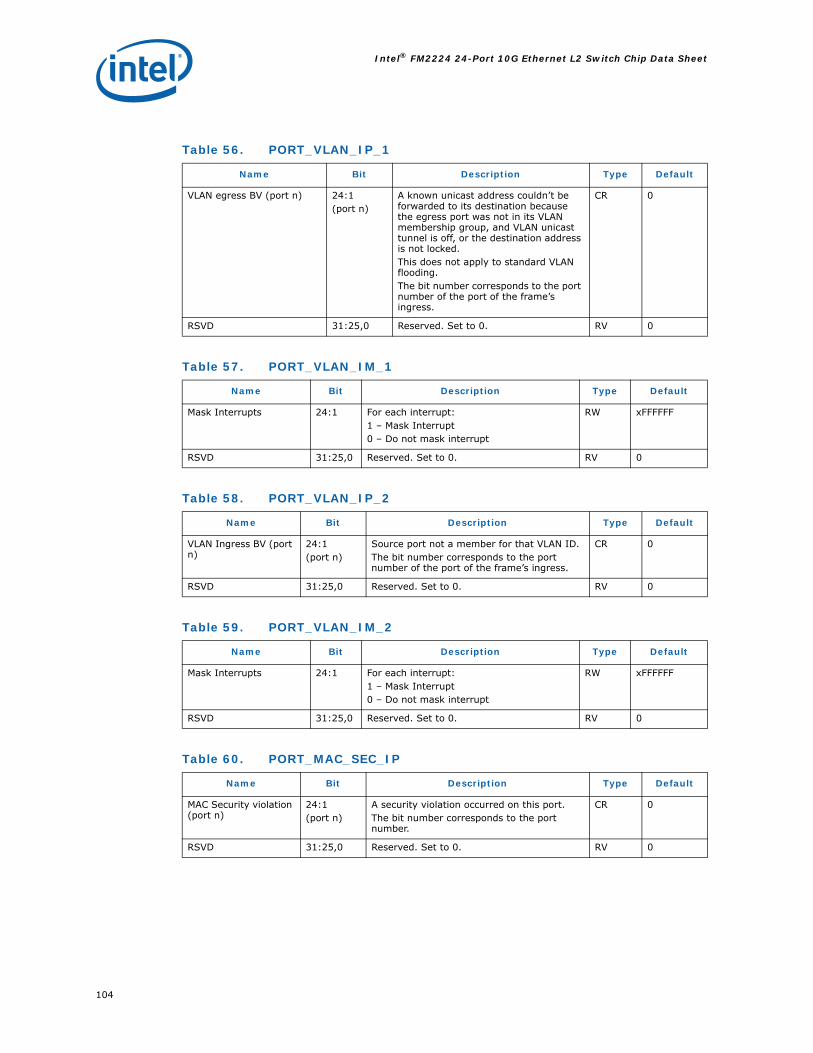
Intel® FM2224 24-Port 10G Ethernet L2 Switch Chip Data Sheet
104
Table 56. PORT_VLAN_IP_1
Name Bit Description Type Default
VLAN egress BV (port n) 24:1(port n)
A known unicast address couldn’t be forwarded to its destination because the egress port was not in its VLAN membership group, and VLAN unicast tunnel is off, or the destination address is not locked.This does not apply to standard VLAN flooding.The bit number corresponds to the port number of the port of the frame’s ingress.
CR 0
RSVD 31:25,0 Reserved. Set to 0. RV 0
Table 57. PORT_VLAN_IM_1
Name Bit Description Type Default
Mask Interrupts 24:1 For each interrupt:1 – Mask Interrupt0 – Do not mask interrupt
RW xFFFFFF
RSVD 31:25,0 Reserved. Set to 0. RV 0
Table 58. PORT_VLAN_IP_2
Name Bit Description Type Default
VLAN Ingress BV (port n)
24:1(port n)
Source port not a member for that VLAN ID. The bit number corresponds to the port number of the port of the frame’s ingress.
CR 0
RSVD 31:25,0 Reserved. Set to 0. RV 0
Table 59. PORT_VLAN_IM_2
Name Bit Description Type Default
Mask Interrupts 24:1 For each interrupt:1 – Mask Interrupt0 – Do not mask interrupt
RW xFFFFFF
RSVD 31:25,0 Reserved. Set to 0. RV 0
Table 60. PORT_MAC_SEC_IP
Name Bit Description Type Default
MAC Security violation (port n)
24:1(port n)
A security violation occurred on this port. The bit number corresponds to the port number.
CR 0
RSVD 31:25,0 Reserved. Set to 0. RV 0

105
Intel® FM2224 24-Port 10G Ethernet L2 Switch Chip Data Sheet
5.4.2 System Configuration
Table 61. PORT_MAC_SEC_IM
Name Bit Description Type Default
Mask Interrupts 24:1 For each interrupt:1 – Mask Interrupt0 – Do not mask interrupt
RW xFFFFFF
RSVD 31:25,0 Reserved. Set to 0. RV 0
Table 62. TRIGGER_IP
Name Bit Description Type Default
Trigger [n] n(15:0)
An interrupt has occurred on Trigger [n] CR 0
RSVD 31:16 Reserved. Set to 0. RV 0
Table 63. TRIGGER_IM
Name Bit Description Type Default
Mask Interrupts 15:0 For each interrupt:1 – Mask Interrupt0 – Do not mask interrupt
RW xFFFF
RSVD 31:16 Reserved. Set to 0. RV 0
Table 64. SYS_CFG_1
Name Bit Description Type Default
Broadcast disable 15 x1 – Discard broadcast framesx0 – Treat broadcast frames normally (see SYS_CFG_1[Broadcast Control]) for further details.
RW 0
Flood control multicast 14 If a multicast address is unknown on destination address look-up, it will be flooded unless this bit is set.
RW 0
Flood control unicast 13 If a unicast address is unknown on destination address look-up, it will be flooded unless this bit is set.
RW 0
RSVD 12:11 Reserved. Set to 0. RV 0
Drop Pause 10 This bit only has an effect when the Ethernet Port Logic is streaming pause into the switch element.x0 – Frames with the MAC control address 01-80-c2-00-00-01 are treated as ordinary multicast (pause pass-through). RxMcast counter is incremented.x1- Frames with the MAC control address 01-80-c2-00-00-01 are discarded (normal Ethernet behavior). RxPause counter is incremented.
RW 1

Intel® FM2224 24-Port 10G Ethernet L2 Switch Chip Data Sheet
106
Remap ET SP15 9 1 – Remap any frame for which the Ether-type = the programmed Ether-type trap to switch priority 150 – Do not do this priority remapping.This only applies if the trap is enabled.
RW 0
Remap CPU SP15 8 1 – Remap any frame for which the destination address = the programmable CPU MAC address to switch priority 15.0 – Do not do this priority remapping.This only applies if the trap is enabled.
RW 0
Remap IEEE SP15 7 1 – Remap any frame with IEEE reserved destination address, or IGMPv3 destination address to Switch Priority 15.0 – Do not do this priority remapping.This only applies if the trap is enabled
RW 1
Broadcast control 6 1 – Send broadcast to the CPU port0 – Do not send the broadcast to the CPU portA broadcast occurs when Destination address = xFFFFFFFFFFFF
RW 1
Trap 802.1x frames 5 1 – Trap frames with destination address = 0x0180C2000003. This may be used in connection with Ether-type trap set to 88-8E
RW 1
Trap IGMP v3 frames 4 1 – IGMPv3 configuration frames will be forwarded to the CPUdestination address = 0x01005E000001.0 – IGMPv3 configuration frames are treated as regular multicast frames
RW 1
Trap GARP frames 3 1 – GARP ports will be forwarded to the CPU0 – GARP frames are treated as regular multicast framesNote: This includes both GMRP and GVRP. Destination address = 0x0180c2000020and destination address = 0x0180C2000021
RW 1
Trap BPDU frames(Enable Spanning Tree)
2 1 – BPDU ports will be forwarded to the CPU.Destination address = 0x0180C2000000.0 – BPDU frames are treated as regular multicast frames
RW 1
Trap LACP and Marker frames (Enable Link aggregation)
1 1 – LACP and Marker frames will be forwarded to the CPU.Destination address = 0x0180C2000002.0 – LACP and Marker frames will be treated as regular multicast frames.
RW 1
Trap Other generic slow protocols
0 1 – Frames of all other IEEE reserved multicast addresses (not enumerated above) will be forwarded to the CPU.Destination address = 0x0180C20000xy: where x==0 & y > 3, x==1, or x==2 & y > 10 – Frames of all other IEEE reserved multicast addresses (not enumerated above) will be treated normally.
RW 1
RSVD 31:16 Reserved. Set to 0. RV 0
Table 64. SYS_CFG_1 (Continued)

107
Intel® FM2224 24-Port 10G Ethernet L2 Switch Chip Data Sheet
Note: If a frame has a destination address = CPU MAC address, then that packet is sent to the CPU regardless of VLAN association.
Table 65. SYS_CFG_2
Name Bit Description Type Default
Multiple Spanning Trees 3 1 – There is one spanning tree per VLAN0 – There is one spanning tree shared by all of the VLANs
RW 0
Enable 802.1q VLAN tagging
2 1 – Use the VLAN table, L2 packet look-up is by MAC address and VLAN. All frames have a VID association. (Either from tag that is already there on Ingress or by port association).Note: VLAN #4095 is reserved.0 – Ignore tags. The tag (or lack of a tag) of the outgoing frame is the same as when the frame Ingressed.There is no notion of a VID in this context. However, the port-based VLAN membership list is stored in the VID table, indexed by port instead of VID.
RW 0
VLAN multicast Tunnel 1 1 – Multicast bit mask is not “anded” with VLAN mask. In IVL mode, the FID address is made “zero” for multicast if the tunnel is on.0 – Multicast bit mask is “anded” with VLAN mask as normal.
RW 0
VLAN unicast Tunnel 0 1 – Unicast bit mask is not “anded” with VLAN membership if the entry is locked in the table.Note: This feature is only efficient in shared learning mode.
RW 0
RSVD 31:4 Reserved. Set to 0. RV 0
Table 66. 66 SYS_CFG_3
Name Bit Description Type Default
CPU MAC address MSB 15:0 Top 16 bits of the CPU MAC address RW x0000
RSVD 31:16 Reserved. Set to 0. RV 0
Table 67. SYS_CFG_4
Name Bit Description Type Default
CPU MAC address LSB 31:0 Bottom 32 bits of the CPU MAC address RW x00000000

Intel® FM2224 24-Port 10G Ethernet L2 Switch Chip Data Sheet
108
Table 68. SYS_CFG_6
Name Bit Description Type Default
Ether-type Trap on 16 1 - Enable Ether-type trap0 – Disable Ether-type trap
RW 0
Ether-type value 15:0 Value of 2 byte ether-type field to be trapped. Any packet with this field will be sent to the CPU instead of forwarded normally. Like IEEE group addresses, this trap takes precedence over VLAN and MAC security. Default is set to type for IEEE 802.1x.
RW x888E
RSVD 31:17 Reserved. Set to 0. RV 0
Table 69. SYS_CFG_7
Name Bit Description Type Default
Disable Aging 31 x1 – Do not age the tablex0 – Age the table with the age time specified below.
RW 0x1
Age Time 30:0 MAC table entry age time, t, in terms of CPU clock periods. Table aging proceeds one entry every 2t periods. The 16K table requires 16K*t*2 periods to complete the aging process.Example:CPU clock 50 MHz (period = 20 ns)Timer set to 0x7530 (decimal 30,000)Entries are aged one per 1.2 ms(30,000*2*20 ns)Entire table aging process occurs in 19.2 sec.
Note: This is a best case calculation. Other activity on the bus takes precedence over aging requests, so actual age timing may be somewhat slower.0x0 – RSVD
RW 0x7530

109
Intel® FM2224 24-Port 10G Ethernet L2 Switch Chip Data Sheet
5.4.3 Per port Configuration
Table 70. PORT_CFG_1 [0..24]
Name Bit Description Type Default
Multiple VLAN Tagging 25 x1 – Treat the incoming frame as if it is untagged for the purpose of VLAN association and tagging. The frame is associated with the per port VLAN default.If the frame leaves the switch tagged in 802.1Q mode, it gets an additional VLAN tag.If the frame leaves the switch untagged in 802.1Q mode, then any original VLAN is preserved, but this tag is not added.Note: If set to 1, VLAN ingress port precedence (bit 19) must also be set to 1.x0 – Single tag only. All of the VLAN rules pertain to the traditional VLAN tag only.
RW 0
Remap Security SP15 24 x1 – Remap a security violation frame that is trapped and sent to the CPU to Switch Priority 15x0 – Do not do this priority remapping
RW 0
Security CFG 23 x0 – Do not trap the frame that caused a security violation. In which case the frame is simply discarded.x1 –Trap the frame and send it to the CPU.Note: Security violations are never forwarded to non-CPU Ethernet ports.
RW 0
MAC security enable 22:21 x0 – No security checksx1 – Unknown source MAC address is considered a security violationx2 – Unknown source MAC address or a source MAC association with another port is a security violation.x3 - reservedNote: Port security is not VLAN aware.
RW 0
Learning Enable 20 1 – Source addresses from this port will be learned.0 - Source addresses from this port will not be learned.
RW 1
VLAN ingress port precedence
19 0 – Tag untagged frames only1 – Overwrite all frames with port default VID and internal switch priority. (Note that egress frame’s priority is still subject to the regeneration bits in TX_PRI_MAP.)
RW 0
Filter ingress VLAN boundary violations
18 1 - If the source port does not match the VLAN membership, it is a VLAN boundary violation and the packet is dropped.0 – Such packet is not dropped.
RW 0
Drop untagged frames 17 1 – Filter frames that do not Ingress with a VLAN tag.0 – Accept frames that do not Ingress with a VLAN tag.Note: If the “Multiple VLAN Tagging” bit is set, then this filter will result in a discard if the incoming frame does not have its first level tag. That is, the ethertype does not equal VLAN.If Ethertype = VLAN but VLAN-ID = 0, the frame is considered untagged.
RW 0
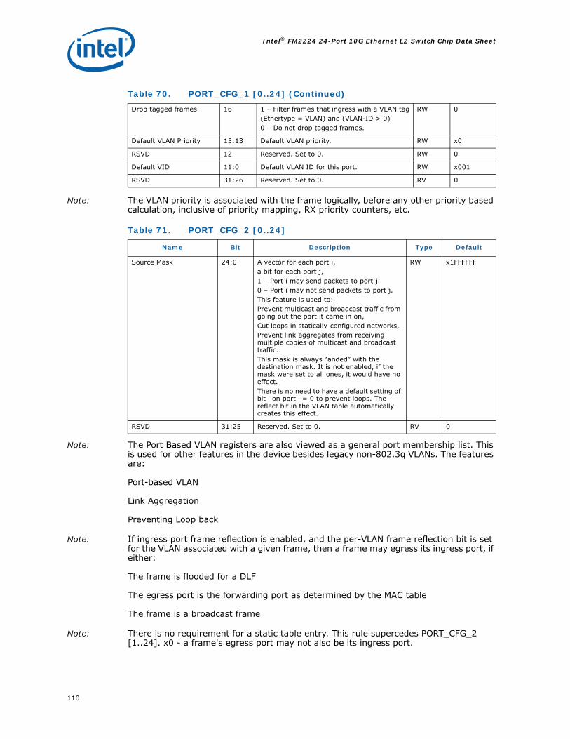
Intel® FM2224 24-Port 10G Ethernet L2 Switch Chip Data Sheet
110
Note: The VLAN priority is associated with the frame logically, before any other priority based calculation, inclusive of priority mapping, RX priority counters, etc.
Note: The Port Based VLAN registers are also viewed as a general port membership list. This is used for other features in the device besides legacy non-802.3q VLANs. The features are:
Port-based VLAN
Link Aggregation
Preventing Loop back
Note: If ingress port frame reflection is enabled, and the per-VLAN frame reflection bit is set for the VLAN associated with a given frame, then a frame may egress its ingress port, if either:
The frame is flooded for a DLF
The egress port is the forwarding port as determined by the MAC table
The frame is a broadcast frame
Note: There is no requirement for a static table entry. This rule supercedes PORT_CFG_2 [1..24]. x0 - a frame's egress port may not also be its ingress port.
Drop tagged frames 16 1 – Filter frames that ingress with a VLAN tag(Ethertype = VLAN) and (VLAN-ID > 0)0 – Do not drop tagged frames.
RW 0
Default VLAN Priority 15:13 Default VLAN priority. RW x0
RSVD 12 Reserved. Set to 0. RW 0
Default VID 11:0 Default VLAN ID for this port. RW x001
RSVD 31:26 Reserved. Set to 0. RV 0
Table 71. PORT_CFG_2 [0..24]
Name Bit Description Type Default
Source Mask 24:0 A vector for each port i,a bit for each port j,1 – Port i may send packets to port j.0 – Port i may not send packets to port j.This feature is used to:Prevent multicast and broadcast traffic from going out the port it came in on,Cut loops in statically-configured networks,Prevent link aggregates from receiving multiple copies of multicast and broadcast traffic.This mask is always “anded” with the destination mask. It is not enabled, if the mask were set to all ones, it would have no effect.There is no need to have a default setting of bit i on port i = 0 to prevent loops. The reflect bit in the VLAN table automatically creates this effect.
RW x1FFFFFF
RSVD 31:25 Reserved. Set to 0. RV 0
Table 70. PORT_CFG_1 [0..24] (Continued)

111
Intel® FM2224 24-Port 10G Ethernet L2 Switch Chip Data Sheet
5.4.4 Non-IEEE 802.3 Header info
Non IEEE-compliant header support comes from two features:• The location of the 16-byte header can be offset in the global per port settings from
the start of packet by any arbitrary byte amount up to 256bytes from the start of the header.
• A bit mask can be applied to any bits in the 16-byte header to generalize the standard source, destination, and type/VLAN fields that would normally exist.
Table 72. HEADER_MASK [0..3]
Name Bit Description Type Default
SWM 31:0 Bit mask for sliding window mask. RW xFFFFFFFF
Table 73. LCI_CFG
Name Bit Description Type Default
RSVD 16:11 Reserved. Set to 0. RV 0
RSVD 10:5 Reserved. Set to 0. RV 0
Host Padding 4 1 – Padding for frames sent from the switch to the host is to 64 bit boundaries.0 – Padding for frames sent from the switch to the host is to 32 bit boundaries.Note: Padding is not required when sending frames from the host to the switch. This feature is to increase compatibility with off-chip DMA engines.
RW 0
Endianess 3 0 – CPU is little Endian.1 – CPU is big Endian.
RW 0
Tx Compute CRC 2 1- Computes the CRC and overwrites the last 4 bytes of the packet with the new CRC.0 – Does not compute the CRC and relies on what the CPU has written in the CRC field.
RW 1
RSVD 1 RV 0
Rx Enable 0 1 – Receive packets in the LCI.0 – Discard all packets in the LCI.Must be set to receive packets into the receive buffer.
RW 0
RSVD 31:17 Reserved. Set to 0. RV 0
Table 74. LCI_ STATUS
Name Bit Description Type Default
RSVD 4 Reserved. Set to 0. RV 0
RSVD 3 Reserved. Set to 0. RV 0
RX EOT 2 1 – Signals end of frame transmission. This bit does not raise an interrupt but it is redundant with the RX end of frame bit in the LCI_IP register. This is done so that software only needs to read one register.
CR 0

Intel® FM2224 24-Port 10G Ethernet L2 Switch Chip Data Sheet
112
Notes: 1. RX Ready itself does not signal new frame or end of frame. Rx Ready could stay high over multiple packets.
2. The TX interrupt is equivalent to a change in state of TX Ready.
Note: See LCI description for treatment of endianness. Endianness only applies to RxData and TxData.
RX Ready 1 1 – Frame data is in the receive FIFO.0 – There is no frame data in the receive FIFO.The transition from 0 to 1 occurs on a new frame. The transition from 1 to 0 occurs at the end of a frame.
RO 0
TX Ready 0 This signal is equivalent to the inverse of Pause. The pause watermarks exist for the switch port, and when pause is triggered this status bit changes to 0. When the port is “unpaused” this bit changes back to 0.Note: it is not anticipated under normal operation, that the CPU port will ever be paused.
RO 1
RSVD 31:5 Reserved. Set to 0. RV 0
Table 75. LCI_RX_FIFO
Name Bit Description Type Default
RxData 31:0 Rx Data channel. All incoming packet data appears on this channel in FIFO order. At the end of the packet the LCI_RX_FRAME_STATUS register data is appended.
RO 0
Table 76. LCI_TX_FIFO
Name Bit Description Type Default
TxData 31:0 Tx Data channel. The CPU or DMA bridge writes exclusively to this register during packet transmission. See LCI functional description for the bit format and “in-band” control fields.
RW 0
Table 77. LCI_IP
Name Bit Description Type Default
LCI_TX Overrun 7 The frame being sent from the manager to the switch was corrupted because the switch did not have room to store the frame.
CR 0
LCI_RX Underflow 6 The frame being sent to the manager under-flowed because all the frame data was not available in the switch quickly enough to keep up with the CPU interface
CR 0
LCI_RX Tail error 5 The frame being sent from the switch to the manager had the error bit set in the fabric
CR 0
LCI_RX Internal Error 4 There was an error on the frame being transmitted from the switch to the manager, however when it entered the switch from the network it was error free. So the switch generated the error.
CR 0
Table 74. LCI_ STATUS (Continued)

113
Intel® FM2224 24-Port 10G Ethernet L2 Switch Chip Data Sheet
Note: By convention:
LCI_RX means frames going to the CPU from the switch which have come from the network.
LCI_TX means frames going from the CPU to the switch on their way to the network.
Bridge Registers
5.4.5 Switch Control Tables
5.4.5.1 MAC Address Table
Address table Fields• Destination Mask - a bit mask of the destination ports to which this address
corresponds.• TRIG-ID - Each trigger has a TRIG-ID defined in TRIGGER_CFG. If the trigger calls
for a single MAC address match, then of the 2 MAC address lookups, there must be one match for that trigger. If the trigger calls for a source address and destination
LCI_RX Error 3 There was an error on the frame being transmitted from the switch to the manager
CR 0
LCI_RX End 2 The switch is done transmitting the packet to the Manager.
CR 0
LCI_RX Request 1 A new packet has arrived for processing. That is, a frame from Ethernet port N > 0 headed for Port 0, has arrived in the switch and needs to be read from the LCI.
CR 0
TXRDY Transition 0 Either of the following two conditions: Change of pause state. The switch had been able to accept new frames from the manager and it no longer can, or vice versa, from a change in pause state.From an overflow in the RX buffer (switch port).
CR 0
RSVD 31:8 Reserved. Set to 0. RV 0
Table 78. LCI_IM
Name Bit Description Type Default
Mask Interrupts 7:0 For each interrupt:1 – Mask Interrupt0 – Do not mask interrupt
RW xFF
RSVD 31:8 Reserved. Set to 0. RV 0
Table 79. MAC Address Table
94:70 69 68 67 66:62 61..50 49..2 1 0
Address Dest. Mask
Age Lock Valid TRIG-ID FID MAC Address RSVD Parity
0
…
16,383
Table 77. LCI_IP (Continued)

Intel® FM2224 24-Port 10G Ethernet L2 Switch Chip Data Sheet
114
address match, then both lookups must resolve to the same TRIG-ID as the trigger lookups.
• Parity - memory protection. A parity error is assumed to be a soft error in the table and is a reason to Reset the chip.
• Age - The age timer. 1 - The entry is new, 0 - The entry is old. Every time the table is accessed the bit is refreshed. If the age clock comes around between refreshes, it purges the table of the entry.
• Valid - The entry is valid.• Lock - The entry may not be aged out of the table. It can only be removed from the
CPU.• FID - Learning Group. In shared spanning tree mode, FID = 0. In multiple spanning
tree mode, FID = VID.• MA Address - MAC address.
Notes: 1. The table is searched by MAC address and FID. That is, the same MAC address may exist once per VLAN in the table in multiple spanning tree mode. On a VLAN boundary violation, an address is not learned.
2. On a parity error, the line is considered invalid.
3. On power-up, all bits are zero by default.
4. MAC entries take 3 32-bit words to completely specify. The entries are aligned to 128 bit boundaries in address space, that is, one entry every four addresses.
Table 80. MA_TABLE_CFG
Name Bit Description Type Default
Hash Rotation 2:1 The hash function produces a 16 bit value. The hash address is only 12 bits. Which 4 bits are excluded is programmable. 0x0 – Bits 15:12 are not used.0x1 – Bits 11:8 are not used.0x2 – Bits 7:4 are not used.0x3 – Bits 3:0 are not used.
RW 0x3
Source address lookup mode
0 1 – The source address lookup is only performed while the frame processor is ahead of the requests for destination address lookups. 0 – The source address lookup is performed on every frame.Note: This mode is incompatible with port security. It is used for achieving high event rate to support forwarding small packets at line rate. Normally, it should be set to 0.
RW 0
RSVD 31:3 Reserved. Set to 0. RV 0

115
Intel® FM2224 24-Port 10G Ethernet L2 Switch Chip Data Sheet
Note: There is a 64-place FIFO behind this. Once the value of the data is read, the register is cleared. If the switch has to place more than 64 changes in the FIFO ahead of the CPU, the FIFO fills up, and the reports of any subsequent table changes will be discarded and the “MA Status Buffer Overflow” interrupt in FRAME_CTRL_IP will be set. This implies that the MAC address table in the switch and the MAC address table in the host software are out of synchronization. The CPU now needs to re-read the entire table, to make the software image of the table consistent.
VLAN Table Fields• VCNT - Check this index, and if VCNT < 32, then VCNT is the index into the
counters for this VLAN to count octets, unicast frames, non-unicast frames in the VLAN.
Table 81. MA_TABLE_STATUS_1
Name Bit Description Type Default
Type 18:16 0x0 – Empty (No new entry since last read).0x1 - Entry was learned.0x2 – Entry was aged.0x3 – Entry was a parity error.0x4-0x7 – RSVD.
CR 0
Last learned/aged entry 15:0 Index of the most recently modified entry in the MAC address table.
CR 0
RSVD 31:19 Reserved. Set to 0 RV 0
Table 82. MA_TABLE_STATUS_2
Name Bit Description Type Default
Bin full count 31:16 Count of times an address was not learned from full bin.
CR 0
Bin Full Hash 11:0 Hash value of last bin that was full. RO 0
RSVD 15:12 Reserved. Set to 0. RV 0
Table 83. MA_TABLE_STATUS_3
Name Bit Description Type Default
Skip LRN count 31:16 Count of the number of times a learning event was skipped because it is best effort and there wasn’t time.
CR 0
Skip source address count
15:0 Count the number of times a source address lookup or learning event was not done because it is best effort and there wasn’t time. (Learning events are always best-effort, source address lookup is only best-effort if the mode bit is set).
CR 0
Table 84. VLAN ID Table
63:14 13 12:8 7:2 1 0
Address Port Membership and Tag RSVD TRIG ID VCNT Reflect Parity
0
…
4094

Intel® FM2224 24-Port 10G Ethernet L2 Switch Chip Data Sheet
116
Parity - If there is a parity error in the VLAN table it is grounds for resetting the chip.
Reflect - If this bit is set then the frame may be sent out the port it came in on, subject to the description in PORT_CFG_1.
TRIG ID - See section on monitoring.
Port Membership and Spanning tree state. 2 bits per port flood map (50 bits).
• b0 - Tag bit— 0 - Frame leaves untagged— 1 - Frame leaves tagged
• b1 - Membership bit — 0 - Port is not a member of this VLAN— 1 - Port is a member of this VLAN
• Port membership includes CPU.
On power-up all bits are zero by default.
In port-based VLAN there is no tagging, however this table is used to store the state of the membership lists. In that case the table is indexed by the port the traffic came in on, instead of the VLAN ID. The tag bit is ignored, as the frame always exits the switch unmodified. The membership bit indicates which ports can receive frames from the source port.
5.4.5.2 Forwarding Information Database (FID) Table
Each FID entry corresponds to a unique spanning tree.
Two bits of spanning tree state per port. This facilitates multiple spanning tree learning.
• Disabled - All packets are discarded in this state. (b1b0=00)• Listening - All packets but BPDUs are discarded in this state. (b1b0=01)• Learning - All packets are discarded, however they are subject to Source lookups
and learning. (b1b0=10)• Fowarding - Port behaves normally. (b1b0=11)
Spanning Tree State does not include CPU (Port 0).
Table 85. FID_TABLE (Spanning Tree State Table)
63:50 49:2 1 0
Address RSVD Spanning Tree State RSVD Parity
0
…
4094
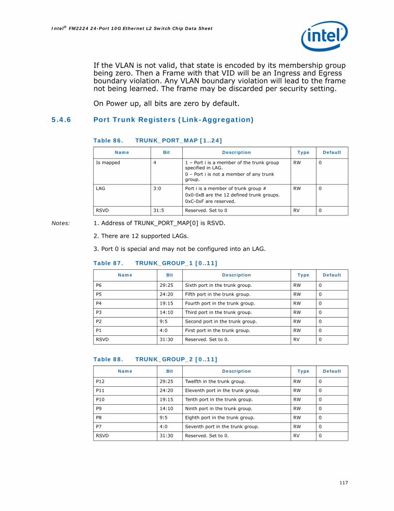
117
Intel® FM2224 24-Port 10G Ethernet L2 Switch Chip Data Sheet
If the VLAN is not valid, that state is encoded by its membership group being zero. Then a Frame with that VID will be an Ingress and Egress boundary violation. Any VLAN boundary violation will lead to the frame not being learned. The frame may be discarded per security setting.
On Power up, all bits are zero by default.
5.4.6 Port Trunk Registers (Link-Aggregation)
Notes: 1. Address of TRUNK_PORT_MAP[0] is RSVD.
2. There are 12 supported LAGs.
3. Port 0 is special and may not be configured into an LAG.
Table 86. TRUNK_PORT_MAP [1..24]
Name Bit Description Type Default
Is mapped 4 1 – Port i is a member of the trunk group specified in LAG.0 – Port i is not a member of any trunk group.
RW 0
LAG 3:0 Port i is a member of trunk group #0x0-0xB are the 12 defined trunk groups. 0xC-0xF are reserved.
RW 0
RSVD 31:5 Reserved. Set to 0 RV 0
Table 87. TRUNK_GROUP_1 [0..11]
Name Bit Description Type Default
P6 29:25 Sixth port in the trunk group. RW 0
P5 24:20 Fifth port in the trunk group. RW 0
P4 19:15 Fourth port in the trunk group. RW 0
P3 14:10 Third port in the trunk group. RW 0
P2 9:5 Second port in the trunk group. RW 0
P1 4:0 First port in the trunk group. RW 0
RSVD 31:30 Reserved. Set to 0. RV 0
Table 88. TRUNK_GROUP_2 [0..11]
Name Bit Description Type Default
P12 29:25 Twelfth in the trunk group. RW 0
P11 24:20 Eleventh port in the trunk group. RW 0
P10 19:15 Tenth port in the trunk group. RW 0
P9 14:10 Ninth port in the trunk group. RW 0
P8 9:5 Eighth port in the trunk group. RW 0
P7 4:0 Seventh port in the trunk group. RW 0
RSVD 31:30 Reserved. Set to 0. RV 0

Intel® FM2224 24-Port 10G Ethernet L2 Switch Chip Data Sheet
118
Notes: 1. The trunk is valid if the length is set to ≥ 1.
2. It is illegal, but not checked in the switch hardware for the following conditions, which will result in undefined behavior:
• A port may not be a member of more than one trunk group.• The CPU port may not be in any trunk group.
The address of TRUNK_CANONICAL[0] is RSVD. Port 0 is not mapped.
Note: The ports in the MAC table are considered canonical and to get a physical port, this is the mapping. Thus to observe a frame coming out a statically mapped physical, the MAC address table must agree with the TRUNK_CANONICAL register.
Table 89. TRUNK_GROUP_3 [0..11]
Name Bit Description Type Default
Group Length 4:0 Number of ports in the trunk group. RW 0
RSVD 31:5 Reserved. Set to 0. RV 0
Table 90. TRUNK_CANONICAL [1..24]
Name Bit Description Type Default
Canonical Port 4:0 The physical port i maps to the canonical port.Valid values are 1 – 24.
RW “I” equal to port number
RSVD 31:5 Reserved. Set to 0. RV 0
Table 91. TRUNK_HASH_MASK
Name Bit Description Type Default
Force Symmetric Hash(A4 and earlier silicon revisions)
6 0x0 – symmetric hash not enabled.0x1 – The hash function will give the same result for:DA=MAC #1 and or SA=MAC #2DA=MAC #2 and or SA=MAC #1When Force Symmetric Hash is applied, the actual value of “Include DA” and “Include SA” are ignored and treated as true. The values of “Include VLAN-ID,” and “Include VLAN-Pri” may be true or false, and should always result in preserving the symmetry. “Include Type and Source” may not be set to 0x2, or symmetry will be broken.
Note: This feature is used for Fat tree topologies where it is desired for the distribution function to resolve to the same uplink port (chip) for both sides of a conversation.
RW 0
Symmetric Hash Mode(A5 and later revisions of silicon)
6 Selects between two independent symmetric hash functions.
Note that “SA Symmetry” and “DA Symmetry” must both be set to 0 to enable symmetric hashing.
RW 0
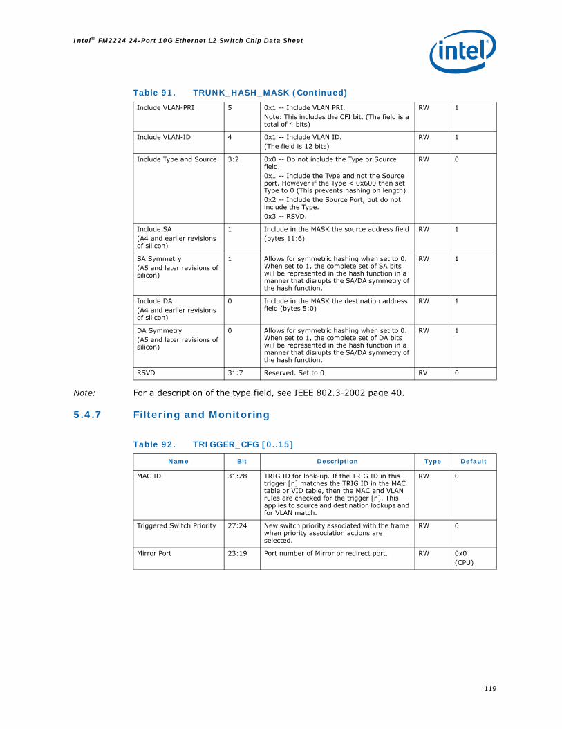
119
Intel® FM2224 24-Port 10G Ethernet L2 Switch Chip Data Sheet
Note: For a description of the type field, see IEEE 802.3-2002 page 40.
5.4.7 Filtering and Monitoring
Include VLAN-PRI 5 0x1 -- Include VLAN PRI.Note: This includes the CFI bit. (The field is a total of 4 bits)
RW 1
Include VLAN-ID 4 0x1 -- Include VLAN ID. (The field is 12 bits)
RW 1
Include Type and Source 3:2 0x0 -- Do not include the Type or Source field.0x1 -- Include the Type and not the Source port. However if the Type < 0x600 then set Type to 0 (This prevents hashing on length)0x2 -- Include the Source Port, but do not include the Type.0x3 -- RSVD.
RW 0
Include SA(A4 and earlier revisions of silicon)
1 Include in the MASK the source address field(bytes 11:6)
RW 1
SA Symmetry(A5 and later revisions of silicon)
1 Allows for symmetric hashing when set to 0. When set to 1, the complete set of SA bits will be represented in the hash function in a manner that disrupts the SA/DA symmetry of the hash function.
RW 1
Include DA(A4 and earlier revisions of silicon)
0 Include in the MASK the destination address field (bytes 5:0)
RW 1
DA Symmetry(A5 and later revisions of silicon)
0 Allows for symmetric hashing when set to 0. When set to 1, the complete set of DA bits will be represented in the hash function in a manner that disrupts the SA/DA symmetry of the hash function.
RW 1
RSVD 31:7 Reserved. Set to 0 RV 0
Table 92. TRIGGER_CFG [0..15]
Name Bit Description Type Default
MAC ID 31:28 TRIG ID for look-up. If the TRIG ID in this trigger [n] matches the TRIG ID in the MAC table or VID table, then the MAC and VLAN rules are checked for the trigger [n]. This applies to source and destination lookups and for VLAN match.
RW 0
Triggered Switch Priority 27:24 New switch priority associated with the frame when priority association actions are selected.
RW 0
Mirror Port 23:19 Port number of Mirror or redirect port. RW 0x0(CPU)
Table 91. TRUNK_HASH_MASK (Continued)

Intel® FM2224 24-Port 10G Ethernet L2 Switch Chip Data Sheet
120
Notes: 1) The default value of source MAC address hit and a source MAC address miss effectively disables the triggers, which is the default state.
2) Trapped frames such as BDPU, GVRP, etc., are not subject to triggers
Action 18:16 0x0 – Forward Normally0x1 – Redirect (send to mirror port only)0x2 – Mirror (send to output port and mirror port)0x3 – Discard.0x4 – Forward normally and associate the frame with the Triggered Switch Priority0x5 – Redirect and associate the frame with the Triggered Switch Priority0x6 – Mirror and associate the frame with the Triggered Switch Priority.0x7 – Reserved.
Note: these actions are mutually exclusive.Note: If the trigger fires, the trigger action is taken on the frame. The first trigger to fire in the precedence order of the trigger number 0..15, is the only trigger taken. There are counts for all triggers.
RW 0
RSVD 15:12 Reserved. Set to 0. RV 0
Any one MAC address match
11 Requires either the source address or the destination address to match, or both.
RW 0
Priority 10 Require frame to have a switch priority match.
RW 0
Multicast 9 Require frame to be multicast. RW 0
Broadcast 8 Require frame to be broadcast. RW 0
Unicast 7 Require frame to be unicast. RW 0
VLAN 6 Require a VLAN trigger match. RW 0
Destination Port 5 Require a destination port mask match. RW 0
Source Port 4 Require a source port mask match. RW 0
Destination MAC miss 3 Require a destination MAC table miss. RW 0
Destination MAC 2 Require a destination MAC trigger match. RW 0
Source MAC miss 1 Require a source MAC table miss. RW 1
Source MAC 0 Require a source MAC table match. RW 1
Table 93. TRIGGER_PRI [0..15]
Name Bit Description Type Default
Priority Mask 15:0 Switch priority mask for this trigger. RW 0
RSVD 31:16 Reserved. Set to 0. RV 0
Table 94. TRIGGER_RX [0..15]
Name Bit Description Type Default
Source Port Mask 24:1 Source port mask for this trigger. RW 0
RSVD 31:25,0 Reserved. Set to 0. RV 0
Table 92. TRIGGER_CFG [0..15] (Continued)
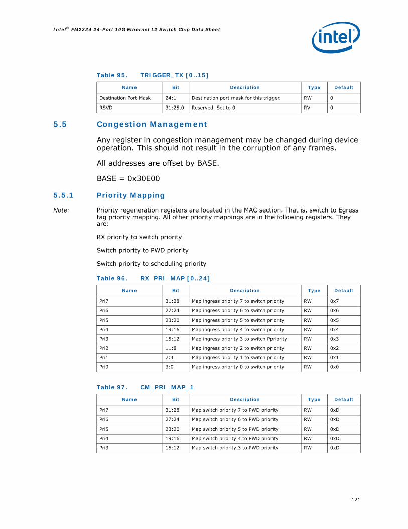
121
Intel® FM2224 24-Port 10G Ethernet L2 Switch Chip Data Sheet
5.5 Congestion Management
Any register in congestion management may be changed during device operation. This should not result in the corruption of any frames.
All addresses are offset by BASE.
BASE = 0x30E00
5.5.1 Priority Mapping
Note: Priority regeneration registers are located in the MAC section. That is, switch to Egress tag priority mapping. All other priority mappings are in the following registers. They are:
RX priority to switch priority
Switch priority to PWD priority
Switch priority to scheduling priority
Table 95. TRIGGER_TX [0..15]
Name Bit Description Type Default
Destination Port Mask 24:1 Destination port mask for this trigger. RW 0
RSVD 31:25,0 Reserved. Set to 0. RV 0
Table 96. RX_PRI_MAP [0..24]
Name Bit Description Type Default
Pri7 31:28 Map ingress priority 7 to switch priority RW 0x7
Pri6 27:24 Map ingress priority 6 to switch priority RW 0x6
Pri5 23:20 Map ingress priority 5 to switch priority RW 0x5
Pri4 19:16 Map ingress priority 4 to switch priority RW 0x4
Pri3 15:12 Map ingress priority 3 to switch Ppriority RW 0x3
Pri2 11:8 Map ingress priority 2 to switch priority RW 0x2
Pri1 7:4 Map ingress priority 1 to switch priority RW 0x1
Pri0 3:0 Map ingress priority 0 to switch priority RW 0x0
Table 97. CM_PRI_MAP_1
Name Bit Description Type Default
Pri7 31:28 Map switch priority 7 to PWD priority RW 0xD
Pri6 27:24 Map switch priority 6 to PWD priority RW 0xD
Pri5 23:20 Map switch priority 5 to PWD priority RW 0xD
Pri4 19:16 Map switch priority 4 to PWD priority RW 0xD
Pri3 15:12 Map switch priority 3 to PWD priority RW 0xD
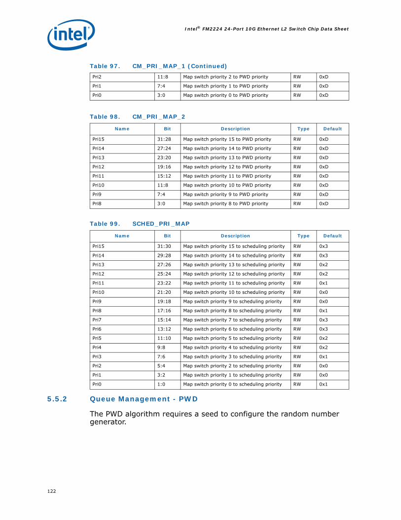
Intel® FM2224 24-Port 10G Ethernet L2 Switch Chip Data Sheet
122
5.5.2 Queue Management - PWD
The PWD algorithm requires a seed to configure the random number generator.
Pri2 11:8 Map switch priority 2 to PWD priority RW 0xD
Pri1 7:4 Map switch priority 1 to PWD priority RW 0xD
Pri0 3:0 Map switch priority 0 to PWD priority RW 0xD
Table 98. CM_PRI_MAP_2
Name Bit Description Type Default
Pri15 31:28 Map switch priority 15 to PWD priority RW 0xD
Pri14 27:24 Map switch priority 14 to PWD priority RW 0xD
Pri13 23:20 Map switch priority 13 to PWD priority RW 0xD
Pri12 19:16 Map switch priority 12 to PWD priority RW 0xD
Pri11 15:12 Map switch priority 11 to PWD priority RW 0xD
Pri10 11:8 Map switch priority 10 to PWD priority RW 0xD
Pri9 7:4 Map switch priority 9 to PWD priority RW 0xD
Pri8 3:0 Map switch priority 8 to PWD priority RW 0xD
Table 99. SCHED_PRI_MAP
Name Bit Description Type Default
Pri15 31:30 Map switch priority 15 to scheduling priority RW 0x3
Pri14 29:28 Map switch priority 14 to scheduling priority RW 0x3
Pri13 27:26 Map switch priority 13 to scheduling priority RW 0x2
Pri12 25:24 Map switch priority 12 to scheduling priority RW 0x2
Pri11 23:22 Map switch priority 11 to scheduling priority RW 0x1
Pri10 21:20 Map switch priority 10 to scheduling priority RW 0x0
Pri9 19:18 Map switch priority 9 to scheduling priority RW 0x0
Pri8 17:16 Map switch priority 8 to scheduling priority RW 0x1
Pri7 15:14 Map switch priority 7 to scheduling priority RW 0x3
Pri6 13:12 Map switch priority 6 to scheduling priority RW 0x3
Pri5 11:10 Map switch priority 5 to scheduling priority RW 0x2
Pri4 9:8 Map switch priority 4 to scheduling priority RW 0x2
Pri3 7:6 Map switch priority 3 to scheduling priority RW 0x1
Pri2 5:4 Map switch priority 2 to scheduling priority RW 0x0
Pri1 3:2 Map switch priority 1 to scheduling priority RW 0x0
Pri0 1:0 Map switch priority 0 to scheduling priority RW 0x1
Table 97. CM_PRI_MAP_1 (Continued)

123
Intel® FM2224 24-Port 10G Ethernet L2 Switch Chip Data Sheet
Note: The degenerate case of the random seed is x7FFFFFFF.
Note: The RX shared watermark and TX shared watermark default to 255 kB, or about 25% of the switch resources. These are “hog watermarks,” protecting the switch from any one port needing too much of the switch resources. This arises during congestion.
Note: The RX private watermark default to 16 kB (0x10), the total amount of private memory is 400 kB for 24 ports, or about 38% of the memory. 16k is chosen to guarantee a jumbo packet may be received on an empty port, irrespective of the congestion of the shared memory. RX private watermark does not enter into the calculation for flow control.
Table 100. LFSR_CFG
Name Bit Description Type Default
Seed 30:0 Random seed. RW 0
RSVD 31 Reserved. Set to 0. RV 0
Table 101. QUEUE_CFG_1 [0..24]
Name Bit Description Type Default
TX Hog WM 25:16 TX queue size, based on 1024 byte values. Frames are dropped 100% at this watermark. Note that a frame causing the WM to be exceeded is not dropped. The next frame considered for that queue is dropped since the WM is now exceeded.
RW 0x0FF
RX Hog WM 9:0 RX queue size, based on 1024 byte values. For Switch. Frames are dropped 100% at this watermark. Note that a frame causing the WM to be exceeded is not dropped. The next frame considered for that queue is dropped since the WM is now exceeded. Should be set higher than the Rx Private WM by at least a max frame size (round up to nearest 1024 byte value).
RW 0x0FF
RSVD 31:26, 15:10
Reserved. Set to 0. RW 0
Table 102. QUEUE_CFG_2 [0..24]
Name Bit Description Type Default
RX Private CFG 15 b1 – Discard frames that fail the TX shared check, even if the RX port associated with that frame has not exceeded its RX private watermark.b0 – Only discard frames that exceed both the TX shared and RX private watermarks.
RW 0
RX Private WM 9:0 RX queue size, based on 1024 byte values. This memory is protected from congestion management for unicast frames.
RW 0x10
RSVD 31:16,14:10
Reserved. Set to 0. RW 0

Intel® FM2224 24-Port 10G Ethernet L2 Switch Chip Data Sheet
124
Note: The low global watermark defaults to leaving about 15% of the memory empty for high priority traffic assuming 16KB RX private FIFOs. The calculation is:
Table 103. QUEUE_CFG_3
Name Bit Description Type Default
Switch Pri WM Select
2*i+1:2*i(15 ≥ i ≥ 0)
0x0 – All frames in this switch priority are checked against the low global watermark for PWD.0x1 – All multicast and broadcast frames in this switch priority are checked against the low global watermark for PWD, but all unicast frames in this switch priority are checked against the high global watermark0x2 – All frames in this switch priority are check against the high global watermark for PWD0x3 – All frames in this switch priority are checked against the privileged watermark only (no PWD).
RW 0x1
Table 104. QUEUE_CFG_4
Name Bit Description Type Default
RSVD 31:28 Reserved. Set to 0. RV 0
Global High Watermark 27:16 Global high watermark based on 1024 byte values. If the frame matches a type in QUEUE_CFG_3 configured to be checked against the high watermark, then the PWD line for that frame intersects this watermark at 100% drop probability.
RW 0x21C
RSVD 15 Reserved. Set to 0. RV 0
RSVD 14:12 Reserved. Set to 0. RV 0
Global low Watermark 11:0 Global low watermark based on 1024 byte values. If the frame matches a type in QUEUE_CFG_3 configured to be checked against the low watermark, then the PWD line for that frame intersects this watermark at 100% drop probability.
RW 0x21C
Table 105. QUEUE_CFG_5
Name Bit Description Type Default
Global Watermark - Privileged
11:0 Global queue size, based on 1024 byte values. All frames are dropped 100% at this watermark.
RW 0x3d0
RSVD 32:12 Reserved. Set to 0. RV 0

125
Intel® FM2224 24-Port 10G Ethernet L2 Switch Chip Data Sheet
Table 106. STREAM_STATUS_1 [0..24]
Name Bit Description Type Default
TX Queue Status 27:16 Number of 1024 byte segments that are occupied in this TX Queue.
RO 0
RX Queue Status 11:0 Number of 1024 byte segments that are occupied in this RX Queue.
RO 0
RSVD 31:28, 15:12
Reserved. Set to 0. RV 0
Table 107. STREAM_STATUS_2
Name Bit Description Type Default
Global Shared Queue Status
27:16 Number of 1024 byte segments that are in the shared portion of the memory. That is, the total memory segment usage minus the segments in the private RX queues.
RO 0
Global Queue Status 11:0 Number of 1024 byte segments that are occupied in the stream memory. Total segments.
RO 0
RSVD 31:28,15:12
Reserved. Set to 0. RV 0
Table 108. EGRESS_SCHEDULE_1 [0..24]
Name Bit Description Type Default
WRR Ports 3:2 Number of ESPQ in strict priority mode, counted from the highest priority ESPQ downward. 0x3 – All queues are WRR.0x2 – The lowest 3 priority queues are WRR.0x1 – The lowest 2 priority queues are WRR.0x0 – All queues are strict priority.Any queues which are not WRR are strict priority. If they are weighted round robin, then the service order and weights are used to determine the scheduling.
RW 0
Service mode 1:0 This only applies to the WRR mode.0x0 – Priority Round Robin.0x1 – Reserved.0x2 – Pure Round Robin.0x3 – RSVD.
RW 0
RSVD 31:4 Reserved. Set to 0. RV 0
Table 109. EGRESS_SCHEDULE_2 [0..24]
Name Bit Description Type Default
Weight Queue 3 31:24 0x01-0xFF - Number of packets per turn in Queue 3.0x00 - Illegal value, undefined behavior.
RW x0F

Intel® FM2224 24-Port 10G Ethernet L2 Switch Chip Data Sheet
126
Note: Weights assigned to queues in Strict Priority mode have no relevance.
The RX pause watermark refers to the total RX status, not the portion of RX status that contributes to the shared memory (RX total - RX private). The defaults for RX_PAUSE_WM are calculated by:
Pause on : 25% of the memory
Pause off: Pause on - 16 kB
The following further restrictions apply to transmitting Pause Frames:• Once the smaller Pause On watermark is achieved (global or per-port), that port
will begin transmitting pause frames.• Once both queues are below their pause off watermarks, that port will end
transmitting pause frames.
Weight Queue 2 23:16 0x01-0xFF - Number of packets per turn in Queue 2.0x00 - Illegal value, undefined behavior.
RW x07
Weight Queue 1 15:8 0x01-0xFF - Number of packets per turn in Queue 1.0x00 - Illegal value, undefined behavior.
RW x03
Weight Queue 0 7:0 0x01-0xFF - Number of packets per turn in Queue 0.0x00 - Illegal value, undefined behavior.
RW x01
Table 110. GLOBAL_PAUSE_WM [0..24]
Name Bit Description Type Default
Pause OFF 27:16 The occupancy of 1024 byte segments in the global shared memory that ends the transmission of Pause frames out of the port. That is, not total memory, but sum of all ports above their RX private watermark.
RW x120
Pause ON 11:0 The occupancy of 1024 byte segments in the global shared memory that initiates the transmission of Pause frames out of the port. In addition, the RX private watermark must be surpassed on any port before it will generate Pause messages.
RW x144
RSVD 31:28, 15:12
Reserved. Set to 0. RV 0
Table 111. RX_PAUSE_WM [0..24]
Name Bit Description Type Default
Pause OFF 27:16 The occupancy of 1024 byte segments in the RX Status that ends the transmission of Pause frames out of the port.
RW x0F5
Pause ON 11:0 The occupancy of 1024 byte segments in the RX Status that initiates the transmission of Pause frames out of the port.
RW x0FF
RSVD 31:28, 15:12
Reserved. Set to 0. RV 0
Table 109. EGRESS_SCHEDULE_2 [0..24] (Continued)
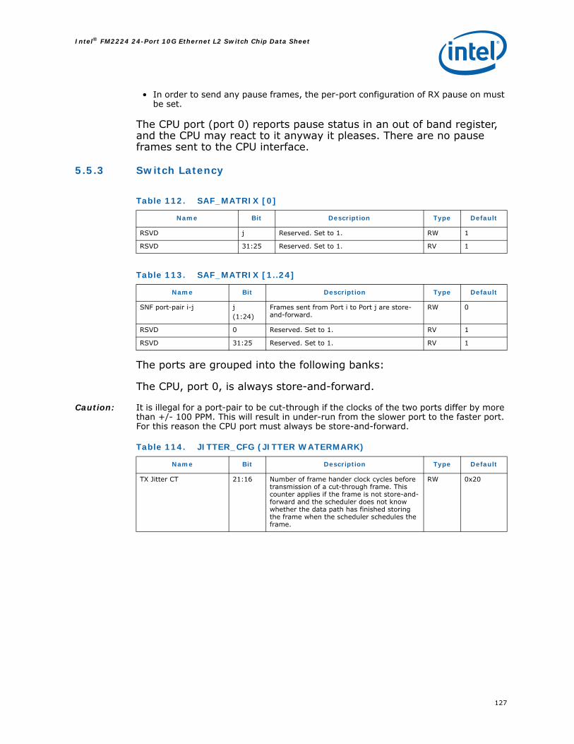
127
Intel® FM2224 24-Port 10G Ethernet L2 Switch Chip Data Sheet
• In order to send any pause frames, the per-port configuration of RX pause on must be set.
The CPU port (port 0) reports pause status in an out of band register, and the CPU may react to it anyway it pleases. There are no pause frames sent to the CPU interface.
5.5.3 Switch Latency
The ports are grouped into the following banks:
The CPU, port 0, is always store-and-forward.
Caution: It is illegal for a port-pair to be cut-through if the clocks of the two ports differ by more than +/- 100 PPM. This will result in under-run from the slower port to the faster port. For this reason the CPU port must always be store-and-forward.
Table 112. SAF_MATRIX [0]
Name Bit Description Type Default
RSVD j Reserved. Set to 1. RW 1
RSVD 31:25 Reserved. Set to 1. RV 1
Table 113. SAF_MATRIX [1..24]
Name Bit Description Type Default
SNF port-pair i-j j(1:24)
Frames sent from Port i to Port j are store-and-forward.
RW 0
RSVD 0 Reserved. Set to 1. RV 1
RSVD 31:25 Reserved. Set to 1. RV 1
Table 114. JITTER_CFG (JITTER WATERMARK)
Name Bit Description Type Default
TX Jitter CT 21:16 Number of frame hander clock cycles before transmission of a cut-through frame. This counter applies if the frame is not store-and-forward and the scheduler does not know whether the data path has finished storing the frame when the scheduler schedules the frame.
RW 0x20

Intel® FM2224 24-Port 10G Ethernet L2 Switch Chip Data Sheet
128
5.6 Statistics
With few exceptions, all counters are 64 bits in the FM2224. The 64-bit counters are stored least significant 32-bit word first (even address). The MIB counters may be read as rarely or often as desired. A MIB counter must be read one at a time. The counters are listed in groups. Each counter in a group is mutually exclusive.
The MIB counters are split into two types: RMON and non-RMON counters. For RMON counters, the FM2224 implements the standard set of counters with no additions or deletions. There are two categories of exceptions to this rule:
• Any counter which is not meaningful in 802.3ae has been deleted. (RxAlignment Errors, TX collisions, etc)
• Packet size bins have been expanded to include some non-standard Ethernet packets, but these bins are only counted if the FM2224 is configured to allow the transmission of non-standard frame sizes.
The FM2224 contains additional counters beyond the traditional RMON MIB definitions. These counters are not targeted at well established software applications. Instead, their definition follows the principle that if the FM2224 has a rule to treat a specific class of packets in a certain way, then that treatment is counted. From this principle follows the security, filtering, and priority based counters, user programmable triggers and VLAN statistics.
5.6.1 Statistics Registers
TX Jitter SF 13:8 Number of frame handler clock cycles before transmission of a frame that meets the following condition:The writing of the frame is at least one segment (256 bytes) ahead of the reading of the frame.Note: This applies to store-and-forward traffic, as well as cut-through traffic that has at least a segment in the memory as a result of switch congestion.
RW 0x20
TX Jitter SS 5:0 Number of EPL clock cycles before starting transmission of a frame that is one sub-segment in length (64 bytes) or less.
RW 0x20
RSVD 31:22, 15:14,7:6
Reserved. Set to 0. RV 0
Table 114. JITTER_CFG (JITTER WATERMARK) (Continued)
Table 115. STATS_CFG
Name Bit Description Type Default
RSVD 11 Reserved. Set to 0 RW 0
RSVD 10 Reserved. Set to 0. RW 0
Group 8 Enable 9 Enable all group 8 counters. RW 1

129
Intel® FM2224 24-Port 10G Ethernet L2 Switch Chip Data Sheet
Note: Port statistics may have difficulty keeping pace when the highest frame rates and smallest frame sizes are present on all ports.
5.6.2 Counter groups
There are 13 groups of counters excluding the extra counters in the Ethernet Port Logic. They are:
Per-port counters (one set per port):• Group 1: RX packet counters per type.• Group 2: RX packet counters per size.• Group 3: RX octet counters.• Group 4: RX packet counters per priority.• Group 5: RX octet counters per priority.• Group 6: RX packet counters per flow.• Group 7: TX packet counters per type.• Group 8: TX packet counters per priority.• Group 9: TX octet counters.
Non-per port counters:• Group 10: Congestion management packet counters (one global set).• Group 11: VLAN octet counters (32 sets, assigned per VLAN).• Group 12: VLAN packet counters (32 sets, assigned per VLAN).• Group 13: Trigger packet counters (16 sets, one per trigger).
Group 7 Enable 8 Enable all group 7 counters. RW 1
RSVD 7 Reserved. Set to 0. RW 0
Group 3 Enable 6 Enable all group 3 counters. RW 1
Group 5 Enable 5 Enable all group 5 counters. RW 1
RSVD 4 Reserved. Set to 0. RW 0
Group 6 Enable 3 Enable all group 6 counters. RW 1
Group 4 Enable 2 Enable all group 4 counters. RW 1
Group 2 Enable 1 Enable all group 2 counters. RW 1
Group 1 Enable 0 Enable all group 1 counters. RW 1
RSVD 31:12 Reserved. Set to 0. RV 0
Table 116. STATS_DROP_COUNT
Name Bit Description Type Default
Drop Count 2 31:16 Number of counter updates in groups 7-9 that were dropped due to counter event rate issues.
CR/W 0
Drop Count 1 15:0 Number of counter updates in groups 1-6 that were dropped due to counter event rate issues.
CR/W 0
Table 115. STATS_CFG (Continued)

Intel® FM2224 24-Port 10G Ethernet L2 Switch Chip Data Sheet
130
Table 117. Group 1 Counters - RX Packet Counters per Type [0..24]
Name Description Address
RxUcast Unicast frames received. (Note: oversize and undersize frames with good or bad CRC are counted. Proper size frames with bad CRC are not counted; they are counted as RxFCSErrors.)
0x70000+0x200*i
RxBcast Valid broadcast frames received (good frames only). 0x70002+0x200*i
RxMcast Valid multicast frames received (good frames only, does not include broadcast or Pause frames).
0x70004+0x200*i
RxPause Valid received pause frames 0x70006+0x200*i
RxFCSErrors Received frames of proper size but CRC error, and integral number of octets.
0x70008+0x200*i
RxSymbolErrors Received frames of proper size, but with symbol error. 0x7000A+0x200*i
Table 118. Group 2 Counters - RX Packet Counters per Size [0..24]
Name Description Address
RxMinto63 Received frames of < 64 octets that are not error frames because the min frame size is set below the Ethernet minimum (good and bad frames counted).
0x70080+0x200*i
Rx64 Received frames of 64 octets (good and bad frames counted).
0x70082+0x200*i
Rx65to127 Received frames of 65 to 127 octets (good and bad frames counted).
0x70084+0x200*i
Rx128to255 Received frames of 128 to 255 octets (good and bad frames counted).
0x70086+0x200*i
Rx256to511 Received frames of 256 to 511 octets (good and bad frames counted).
0x70088+0x200*i
Rx512to1023 Received frames of 512 to 1023 octets (good and bad frames counted).
0x7008A+0x200*i
Rx1024to1522 Received frames of 1024 to 1522 octets (good and bad frames counted).
0x7008C+0x200*i
Rx1523to2047 Received frames of 1523 to 2047 octets (good and bad frames counted).
0x7008E+0x200*i
Rx2048to4095 Received frames of 2048 to 4095 octets (good and bad frames counted).
0x70090+0x200*i
Rx4096to8191 Received frames of 4096 to 8191 octets (good and bad frames counted).
0x70092+0x200*i
Rx8191to10239 Received frames of 8192 to 10239 octets (good and bad frames counted).
0x70094+0x200*i
Rx10240toMax Received frames of 10240 to MaxFrame octets. Note: Maxframe is configurable. This counter will only be activated if MaxFrame is > 10240. That is it is the count of non-error frames above 10240. In any case, Intel® strongly recommends against sending packets above 10240 octets, as the Ethernet CRC is no longer valid.
0x70096+0x200*i
RxFragments Received frames smaller than Min Sized Frame octets with either a CRC or alignment error.
0x7009C+0x200*i

131
Intel® FM2224 24-Port 10G Ethernet L2 Switch Chip Data Sheet
RxUndersized Received frames smaller than the minimum frame size but otherwise well formed with a good CRC.
0x70098+0x200*i
RxJabbers Received frames greater than MaxFrame octets and alignment error and good or bad CRC. This counter is only 16 bits.
0x80029+0x400*(N-1)
RxOversized Received frames greater than MaxFrame octets . This counter includes oversized well formed packets as well oversized packets with bad a CRC or an alignment problem. The software must read the counter STAT_RX_JABBER[Jabber Count] in the EPL to detect how many of the oversized frames where actually malformed packets. NOTE: If the frame is counted here, it is not counted in a bin counter RxXXXXtoYYYY even if it fits in that bin.
0x7009A+0x200*i
Table 119. Group 3 Counters - RX Octet Counters [0..24]
Name Description Address
RxGoodOctets Received octets on good packets. 0x700A0+0x200*i
RxBadOctets Received octets on bad packets. Note: total received octets is the sum of RxGoodOctets and RxBadOctets.
0x700A2+0x200*i
Table 120. Group 4 Counters - RX Packet Counters per Priority [0..24]
Name Description Address
RxP0 Received frames of priority 0. 0x70010+0x200*i
RxP1 Received frames of priority 1. 0x70012+0x200*i
RxP2 Received frames of priority 2. 0x70014+0x200*i
RxP3 Received frames of priority 3. 0x70016+0x200*i
RxP4 Received frames of priority 4. 0x70018+0x200*i
RxP5 Received frames of priority 5. 0x7001A+0x200*i
RxP6 Received frames of priority 6. 0x7001C+0x200*i
RxP7 Received frames of priority 7. 0x7001E+0x200*i
Table 121. Group 5 Counters - RX Octet Counters per Priority [0..24]
Name Description Address
RxOctetsP0 Received octets on Priority 0. 0x70120+0x200*i
RxOctetsP1 Received octets on Priority 1. 0x70122+0x200*i
RxOctetsP2 Received octets on Priority 2. 0x70124+0x200*i
RxOctetsP3 Received octets on Priority 3. 0x70126+0x200*i
RxOctetsP4 Received octets on Priority 4. 0x70128+0x200*i
RxOctetsP5 Received octets on Priority 5. 0x7012A+0x200*i
RxOctetsP6 Received octets on Priority 6. 0x7012C+0x200*i
RxOctetsP7 Received octets on Priority 7. 0x7012E+0x200*i
Table 118. Group 2 Counters - RX Packet Counters per Size [0..24]

Intel® FM2224 24-Port 10G Ethernet L2 Switch Chip Data Sheet
132
Table 122. Group 6 Counters - RX Packet Counters per Flow [0..24]
Name Description Address
FIDForwarded Number of frames that were forwarded normally, either unicast or multicast, as a result of a lookup of a valid entry in the MAC address table, or a broadcast. Note: This counter does not count mirrored frames.
0x70100+0x200*i
FloodForwarded Number of good unicast addressed frames that were flooded because the destination is unknown, or an unregistered multicast.
0x70102+0x200*i
TriggerMirrored Number of good frames that were mirrored. Note: Total number of normally forwarded packets = FIDForwarded + FloodForwarded + TriggerMirrored (note that trapped frames are not subject to triggers, so are not mirrored). This counter is only incremented if flooding is enabled in the switch..
0x70112+0x200*i
STPDrops Number of frames that were dropped because either the ingress or egress port is not in the forwarding spanning tree state, resulting in a frame drop on ingress.
0x70104+0x200*i
ReservedTraps Number of frames that are trapped to the CPU and not forwarded normally, as a result of any of the three specific trap functions: Destination address = IEEE reserved group address (as configured in SYS_CFG_1)Destination address = CPU MAC address (as configured in SYS_CFG_3 and SYS_CFG_4)Ether-type = Ether-type trap (as configured in SYS_CFG_6)
0x70106+0x200*i
BroadcastDrops Number of frames that were dropped with DA=xFFFFFFFFFFFF because storm control is enabled.
0x70116+0x200*i
SecurityViolationDrops Number of frames that are dropped or trapped because they are considered a security violation.
0x70108+0x200*i
VLANTagDrops Number of frames discarded because the frames were untagged, and drop untagged is configured, or the frames were tagged, and drop tagged is configured.
0x7010A+0x200*i
VLANIngressBVDrops Number of frames dropped for an Ingress VLAN boundary violation. Note: This only applies to 802.1Q, because in port-based VLAN there is no such thing as an ingress violation.
0x7010C+0x200*i
VLANEgressBVDrops Number of frames dropped for an Egress VLAN boundary violation. This does not mean the number of ports filtered by the VLAN membership list in a multicast or flood; it means the destination address corresponds to a port that is not (or no longer) in the VLAN membership list, so the frame was dropped and not forwarded.
0x7010E+0x200*i
TriggerRedirAndDrops Number of frames that were dropped or redirected because they caused a user defined trigger to fire.
0x70110+0x200*i
DLFDrops Number of frames that were discarded because there was a destination lookup failure and flooding is not enabled in the switch. Note: This counter is incremented for unicast. & multicast
0x70114+0x200*i
CMRxDrops Number of frames dropped for exceeding the RX shared watermark.
0x70118+0x200*i

133
Intel® FM2224 24-Port 10G Ethernet L2 Switch Chip Data Sheet
Table 123. Group 7 Counters - TX Packet Counters per Type [0..24]
Name Description Address
TxUnicast Unicast frames transmitted, possibly with incorrect FCS due to cut-through. (Note: undersized frames that have been padded to the min size (MAC_CFG_2[PadMinSize]=1) are counted.)
0x70020+0x200*i
TxBroadcast Broadcast frames transmitted, possibly with incorrect FCS due to cut-through.
0x70022+0x200*i
TxMulticast Multicast frames transmitted, possibly with incorrect FCS due to cut-through.
0x70024+0x200*i
TxPause Transmitted pause frames, and valid FCS.This counter is a 32 bit counter only. Also described in .
0x80026+0x400*(N-1)
TxFCSErrors Transmitted frames with FCS errors. (Note: undersized frames that have been padded to the min size (MAC_CFG_2[PadMinSize]=1) are not counted even thought they have a forced bad CRC.)This counter is a 32 bit conter only. Also described in
0x80027+0x400*(N-1)
TxErrorDrops The number of frames that the were marked on ingress as erroneous (either due to an FCS or PHY error, or due to under/over size problems) which the switch element actually managed to discard. Frames marked as erroneous on ingress which were transmitted (due to cut-through) will not be included in this counter.
0x70028+0x200*i
TxTimeoutDrops A frame in a TX queue was drop as a result of a time out.
0x70026+0x200*i
Table 124. Group 8 Counters - TX Packet Counters per Size [0..24]*
Name Description Address
TxMinto63 Transmitted frames of min frame size to 63 octets. This counter is for non-error frames that are less than 64 octets because the min frame size is set below 64 octets in the MAC, or error frames that the switch transmitted anyway because MAC_CFG_2[Min Frame Discard] was not set (includes bad frames)
0x700A8+0x200*i
Tx64 Transmitted frames of 64 octets. (includes bad frames) 0x700AA+0x200*i
Tx65to127 Transmitted frames of 65 to 127 octets. (includes bad frames)
0x700AC+0x200*i
Tx128to255 Transmitted frames of 128 to 255 octets. (includes bad frames)
0x700AE+0x200*i
Tx256to511 Transmitted frames of 256 to 511 octets. (includes bad frames)
0x700B0+0x200*i
Tx512to1023 Transmitted frames of 512 to 1023 octets. (includes bad frames)
0x700B2+0x200*i
Tx1024to1522 Transmitted frames of 1024 to 1522 octets. (includes bad frames)
0x700B4+0x200*i
Tx1523to2047 Transmitted frames of 1522 to 2047 octets. (includes bad frames)
0x700B6+0x200*i
Tx2048to4095 Transmitted frames of 2048 to 4095 octets. (includes bad frames)
0x700B8+0x200*i

Intel® FM2224 24-Port 10G Ethernet L2 Switch Chip Data Sheet
134
Note: Packet lengths are calculated before any frame length modifications are made by the EPL (Ethernet Port Logic) such as VLAN tag removal, for example.
Note: 0 ≤ i ≤ 31. See VCNT field in VID table. This is the index i.
Tx4096to8191 Transmitted frames of 4096 to 8191 octets. (includes bad frames)
0x700BA+0x200*i
Tx8192to10239 Transmitted frames of 8192 to 10239 octets. (includes bad frames)
0x700BC+0x200*i
Tx10240toMax Transmitted frames of 10240 to MaxFrame octets. (includes bad frames). This counter will only be activated if Maxframe is > 10240. That is it is the count of non-error frames above 10240. However, Intel® strongly recommends not sending packets above 10240, as the Ethernet CRC isn’t long enough.
0x700BE+0x200*i
Table 125. Group 9 Counters - TX Octet Counters [1..24]
Name Description Address
TxOctets Transmitted octets including CRC but excluding preambles and inter-frame characters.
Port 1…N:0x802C + 0x400*(i-1)
Table 126. Group 10 Counters - Congestion Management Counters
Name Description Address
CMTxDrops[0..24] Count of frames dropped for congestion management from TX port 0.
0x66080+2*i
CMGlobalLowDrops Count of frames dropped for congestion management from the global low PWD watermark.
0x66000
CMGlobalHighDrops Count of frames dropped from the global high PWD watermark.
0x66002
CMGlobalPrivilegeDrops Count of frames dropped from the global privilege watermark.
0x66004
Table 127. Group 11 Counters - VLAN Octet Counters [0..31]
Name Description Address
VLANUnicastOctets[i] Unicast octets received on VLAN[i]. 0x66180+2*i
VLANXcastOctets[i] Broadcast and multicast octets received on VLAN[i]. 0x661C0+2*i
Table 128. Group 12 Counters - VLAN Packet Counters [0..31]
Name Description Address
VLANUnicast[i] Unicast frames received on VLAN[i] 0x66100+2*i
VLANXcast[i] Broadcast and multicast frames received on VLAN[i] 0x66140+2*i
Table 129. Group 13 Counters - Trigger Counters [0..16]
Name Description Address
TrigCount[i] Number of times trigger “I” was taken, where 0 ≤ i ≤ 15. 0x660C0+2*i
TrigCount[16] No trigger was taken. 0x660E0
Table 124. Group 8 Counters - TX Packet Counters per Size [0..24]*
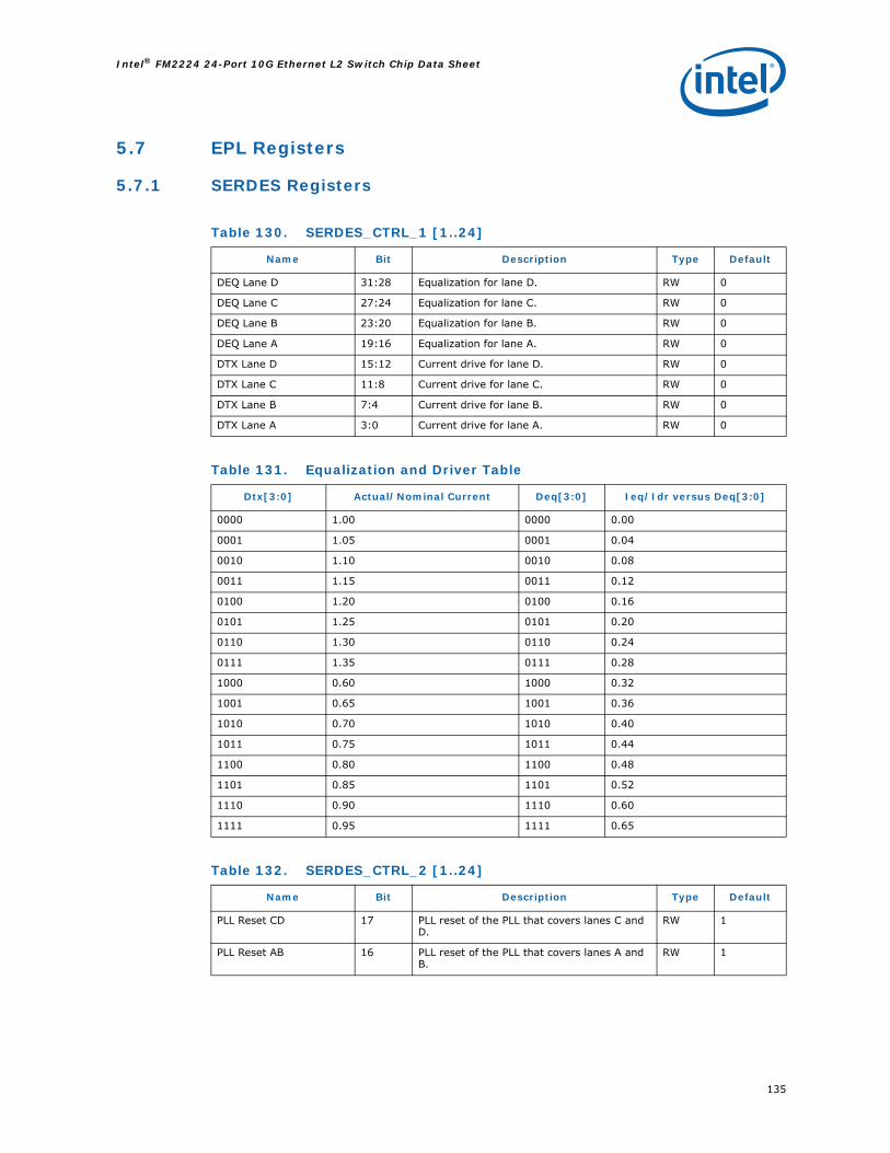
135
Intel® FM2224 24-Port 10G Ethernet L2 Switch Chip Data Sheet
5.7 EPL Registers
5.7.1 SERDES Registers
Table 130. SERDES_CTRL_1 [1..24]
Name Bit Description Type Default
DEQ Lane D 31:28 Equalization for lane D. RW 0
DEQ Lane C 27:24 Equalization for lane C. RW 0
DEQ Lane B 23:20 Equalization for lane B. RW 0
DEQ Lane A 19:16 Equalization for lane A. RW 0
DTX Lane D 15:12 Current drive for lane D. RW 0
DTX Lane C 11:8 Current drive for lane C. RW 0
DTX Lane B 7:4 Current drive for lane B. RW 0
DTX Lane A 3:0 Current drive for lane A. RW 0
Table 131. Equalization and Driver Table
Dtx[3:0] Actual/Nominal Current Deq[3:0] Ieq/Idr versus Deq[3:0]
0000 1.00 0000 0.00
0001 1.05 0001 0.04
0010 1.10 0010 0.08
0011 1.15 0011 0.12
0100 1.20 0100 0.16
0101 1.25 0101 0.20
0110 1.30 0110 0.24
0111 1.35 0111 0.28
1000 0.60 1000 0.32
1001 0.65 1001 0.36
1010 0.70 1010 0.40
1011 0.75 1011 0.44
1100 0.80 1100 0.48
1101 0.85 1101 0.52
1110 0.90 1110 0.60
1111 0.95 1111 0.65
Table 132. SERDES_CTRL_2 [1..24]
Name Bit Description Type Default
PLL Reset CD 17 PLL reset of the PLL that covers lanes C and D.
RW 1
PLL Reset AB 16 PLL reset of the PLL that covers lanes A and B.
RW 1

Intel® FM2224 24-Port 10G Ethernet L2 Switch Chip Data Sheet
136
Note: The 2-bit number constructed from 1 bit per lane of the Low Drive field and one bit per lane of the High Drive field is used to encode the nominal drive current, according to the following table:
Lane Power Down 15:12 Independent lane power down. 1 bit per lane.Note: The FM2224 operates in 4 lane or 1 lane modes only. In the one lane mode, only lane 0 or lane 3 will be enabled.
RW b1111
Lane Reset 11:8 Independent lane reset. 1 bit per lane. RW b1111
High Drive 7:4 1 bit per lane. See table. RW 0
Low Drive 3:0 1 bit per lane. See table. RW 0
RSVD 31:18 Reserved. Set to 0. RV 0
Table 133. Nominal SERDES Drive Current
HiDrv LoDrv Nominal Driver Current
0 0 20mA
0 1 10mA
1 0 28mA
1 1 Reserved
Table 134. SERDES_CTRL_3 [1..24]
Name Bit Description Type Default
DC 19:0 Lane locked and signal detect de-assertion count. Number of cycles to count before de-asserting SD bit in SERDES STATUS register. (CX4 spec is 250us) and LU in PCS Status register (default: 78,125)
RW x1312D
RSVD 31:20 Reserved. Set to 0. RV 0
Table 135. SERDES_TEST_MODE [1..24]
Name Bit Description Type Default
FE 6 Enables PCS framer.The function of the PCS framer is to look for the comma character and instruct the SERDES I/O to shift by a certain number of bits when the comma character is not properly aligned. The PCS framer must be enabled at all time except during SERDES testing using BIST.
RW 1
BS 5 Synchronizes the RX BIST checker. When register de-asserted allows RX BIST to start checking. Change in state is delayed by 5 cycles to allow for starting of pattern through setting BM and also de-assertion the BS bit.
RW 1
Table 132. SERDES_CTRL_2 [1..24] (Continued)

137
Intel® FM2224 24-Port 10G Ethernet L2 Switch Chip Data Sheet
Test Mode 4:3 Test Mode0x0 – normal -default0x1 - Parallel Loop-back0x2-0x3 – RSVD
RW 0
BIST Mode 2:0 0x0 – Disabled 0x1 – PRBS, Test Data = x9+x5+10x2 – Test Data = D21.5 Pattern0x3 – Test Data = K28.5(Idle) Pattern0x4 – Test Data = K28.7(Test) Pattern0x5 – PRBS, Test Data = x10+x3+10x6 – PRBS, Test Data = x9+x4+1 0x7 – PRBS, Test Data = X7+1
RW 0
RSVD 31:6 Reserved. Set to 0. RV 0
Table 136. SERDES_STATUS [1..24]
Name Bit Description Type Default
Signal Detect 4 Signal Detect based on all four lanes. There is hysteresis in this status, see SERDES_CTRL_3.In 1 lane mode, the Signal detect is only based on lane 0 or lane 3, depending the lane reversal state.Note that when in SerDes Loopback mode, Signal Detect is achieved but not displayed via this bit.
RO 0
Symbol Lock 3:0 Symbol Lock. 1 bit per lane.In 1 lane mode only the 1 active lane should be read for polling the lock status. The other 3 bits are undefined.
RO 0
RSVD 31:5 Reserved. Set to 0. RV 0
Table 137. SERDES_IP [1..24]
Name Bit Description Type Default
EC 31:12 Saturating Error counter – increments once per any kind of error in any lane. For instance if all 12 errors(3 per lane) were asserted the Error count would increment by 1
CR 0
ER3DE 11 Lane 3 Disparity Error. CR 0
ER3BC 10 Lane 3 Out of band Character. CR 0
ER3LS 9 Lane 3 Loss of Signal. CR 0
ER2DE 8 Lane 2 Disparity Error. CR 0
ER2BC 7 Lane 2 Out of band Character. CR 0
ER2LS 6 Lane 2 Loss of Signal. CR 0
ER1DE 5 Lane 1 Disparity Error. CR 0
ER1BC 4 Lane 1 Out of band Character. CR 0
ER1LS 3 Lane 1 Loss of Signal. CR 0
ER0DE 2 Lane 0 Disparity Error. CR 0
ER0BC 1 Lane 0 Out of band Character. CR 0
ER0LS 0 Lane 0 Loss of Signal. CR 0
Table 135. SERDES_TEST_MODE [1..24] (Continued)

Intel® FM2224 24-Port 10G Ethernet L2 Switch Chip Data Sheet
138
Note: The interrupt detect field for SERDES_IP is only the OR of bits 11:0. Not the counter.
5.7.2 PCS Registers
Table 138. SERDES_IM [1..24]
Name Bit Description Type Default
Interrupt Mask 11:0 1 – Mask interrupt.0 – Do not mask interrupt.
RW XFFF
RSVD 31:12 Reserved. Set to 0. RV 0
Table 139. SERDES_BIST_ERR_CNT [1..24]
Name Bit Description Type Default
BEC 31:0 8 bits per lane. Saturating counter. CR 0
Table 140. PCS_CFG_1 [1..24]
Name Bit Description Type Default
RSVD 31 Reserved. Set to 0 RV 0
DS 30:29 Datapath structure2’b00: 4lanes (10Gb)2’b01: 1 lane (1Gb)2’b10: 1 lane – 1/10 effective data rate (100Mb)2’b11: 1 lane – 1/100 effective data rate (10Mb)
RW 0
AA 28 Arbitration scheme1’b0: Fast Arbitration – used when EPL datapath frequency is the highest in the chip1’b1: Slow Arbitration – used when EPL datapath is slower frequency and do not want to buffer up header data before arbitrating.
RW 1
DR 27 Disable Receive RS. This will stop accepting data from the MAC.
RW 0
DT 26 Disable Transmit RS. RW 0
FS 25 Force Sequence Ordered Set Note: Cleared when FSIG is sent and will also cause FS bit to be asserted in PCS_IP Register
RW 0
FR 24 Force Remote Fault. Will force transmission of remote fault symbol continuously.
RW 0
FL 23 Force Local Fault. Will force transmission of local fault symbol continuously.
RW 0
EL 22 Enabling sending remote fault in response to RX link being down
RW 0
EF 21 Enable sending of remote faults on RX and also allow the disabling of TX channel when 4 or more RF seen
RW 0
RI 20 Invert RX lane ordering (L3 – L0)In 1 lane mode this recieves all data on lane 3 instead of lane 0
RW 0

139
Intel® FM2224 24-Port 10G Ethernet L2 Switch Chip Data Sheet
TI 19 Invert TX lane ordering (L3-L0)In 1 lane mode this sends all data out on lane 3 instead of lane 0
RW 0
DE 18 Enables the deficit idle count. The DIC counter allows an average of the programmed IFG, usually taken as 12, while forcing alignment of the start of frame to lane zero.
RW 0
II 17 Ignore inter-frame gap errors(Recommend setting this bit, especially in single serdes mode.)
RW 0
IP 16 Ignore Preamble Errors(Recommend setting this bit, especially in single serdes mode.)
RW 0
ID 15 Ignore Data Errors. These are non-data characters found within the frame - bounded by |S| and |T|
RW 0
IA 14 Ignore All RX errors RW 0
IF 13:8 Programmable inter-frame gap (6b – 0-63B) Transmit only.
RW 0xC
RSVD 7:5 Reserved. Set to 0. RV 0
SP 4 Enable support of shorter preamble in 10M/100M/1G mode only. Do not set this option in 10G mode.
RW 0
LF 3:0 LFSR seed, used to randomize /K/R/A characters in 10G mode. Must be non-zero; 0xA works well.
RW 0xA
Table 141. PCS_CFG_2 [1..24]
Name Bit Description Type Default
LF 23:0 Local fault value.The default value is required for compliance to 802.3ae.
RW x000001
RSVD 31:25 Reserved. Set to 0. RV 0
Table 142. PCS_CFG_3 [1..24]
Name Bit Description Type Default
RF 23:0 Remote fault valueThe default value is required for compliance to 802.3ae.
RW x000002
RSVD 31:24 Reserved. Set to 0. RV 0
Table 143. PCS_CFG_4 [1..24]
Name Bit Description Type Default
FSIGTX 23:0 Transmit FSIG value RW x000000
RSVD 31:24 Reserved. Set to 0. RV 0
Table 140. PCS_CFG_1 [1..24] (Continued)

Intel® FM2224 24-Port 10G Ethernet L2 Switch Chip Data Sheet
140
Table 144. PCS_CFG_5 [1..24]
Name Bit Description Type Default
FSIGRX 23:0 Received FSIG value RO X000000
RSVD 31:24 Reserved. Set to 0. RV 0
Table 145. PCS_IP [1..24]
Name Bit Description Type Default
Fault change 14 Indicates that there was a local fault or remote fault status change on the line. Read the LF or RF bit to determine the current status.
CR 0
Link Up 13 This bit reflects the current status of the link.
If this bit is set, then the link is in good working order, i.e. signal is detected (SERDES Status[SD]), symbol locked (SERDES Status[SL]) and lanes are aligned (PCS Status[LA]).
Hysteresis on this signal is controlled by registger SERDES_CONTROL_3
RO 0
Link went up 12 Link transitioned from being down to being up
CR 0
Link went down 11 Link transitioned from being up to being down
CR 0
OV3 10 PCS FIFO overflow Lane 3 CR 0
OV2 9 PCS FIFO overflow Lane 2 CR 0
OV1 8 PCS FIFO overflow Lane 1 CR 0
OV0 7 PCS FIFO overflow Lane 0 CR 0
LA 6 Lanes Mis-AlignedShould be masked in 1 lane mode
CR 0
FSIG Sent 5 FSIG Sent CR 0
RS 4 Remote fault sent CR 0
LS 3 Local fault sent CR 0
FD 2 FSIG detected CR 0
RD 1 Remote Fault Detected. This is a status bit, not an interrupt bit.The switch set this bit when at least 4 RF symbols are received from the line within 128 cycles.The switch reset this bit when no RF symbols are received within 128 cycles.
RO 0
LD 0 Local Fault Detected. This is a status bit, not an interrupt bit.The switch set this bit when at least 4 LF symbols are received from the line within 128 cycles.The switch reset this bit when no LF symbols are received within 128 cycles.
RO 0
RSVD 31:15 Reserved. Set to 0. RV 0

141
Intel® FM2224 24-Port 10G Ethernet L2 Switch Chip Data Sheet
Note: At the link level, frames can no longer be re-ordered. So if the scheduler picks a frame to transmit that can't go because of the IFGS and the frame priority, it is not acceptable for a higher priority frame behind it to be transmitted first even if it meets the watermark check in EPL_PACE_PRI_WM[i].
The index used [0..7] is retrieved from the switch priority to egress priority table TXPRI_MAP regardless if the priority regeneration is enabled or not.
Table 146. PCS_IM [1..24]
Name Bit Description Type Default
Interrupt Mask 14:0 1 – Mask interrupt0 – Do not mask interrupt
Note that bits 0, 1 and 13 correspond to status bits in the PCS_IP register and shall remain masked.
RW X7FFF
RSVD 31:15 Reserved. Set to 0. RV 0
Table 147. PACING_PRI_WM [0..7] [1..24]
Name Bit Description Type Default
Pace_WM[i] 24:0 Watermark (in 4 byte words). For a frame of IEEE 802.1p, the WM is checked against the IFGS. If the IFGS has exceeded this WM, then the frame is held on transmission until the IFGS has been decremented to this WM.*
In 1 lane mode will increment counter by 4B for each cycle actual data is sent. One can think of the counter to be an effectively 23b byte counter. 1 lane 1/10 and 1/100 mode operation will be ignored and will make IFGS ineffective for these 2 modes.
RW x0000
RSVD 31:25 Reserved. Set to 0. RV 0
Table 148. PACING_RATE [1..24]
Name Bit Description Type Default
Pacing Rate 7:0 Pacing Rate controls the rate to a degree of 1 in 256. 0x00 – Pacing is not enabled0x01 – Pacing is 1/256 the bandwidth.…0xFF – Pacing is 255/256 the bandwidth
RW x00
RSVD 31:8 Reserved. Set to 0. RV 0
Table 149. PACING_STAT [1..24]
Name Bit Description Type Default
IFGS 24:0 IFGS (calculated in bytes) from each frame accumulated from frame to frame.
RO x0000
RSVD 31:25 Reserved. Set to 0. RV 0
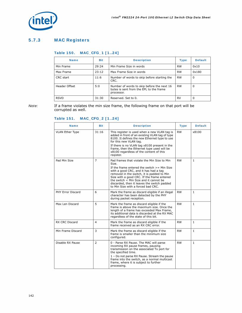
Intel® FM2224 24-Port 10G Ethernet L2 Switch Chip Data Sheet
142
5.7.3 MAC Registers
Note: If a frame violates the min size frame, the following frame on that port will be corrupted as well.
Table 150. MAC_CFG_1 [1..24]
Name Bit Description Type Default
Min Frame 29:24 Min Frame Size in words RW 0x10
Max Frame 23:12 Max Frame Size in words RW 0x180
CRC start 11:6 Number of words to skip before starting the CRC.
RW 0
Header Offset 5:0 Number of words to skip before the next 16 bytes is sent from the EPL to the frame processor.
RW 0
RSVD 31:30 Reserved. Set to 0. RV 0
Table 151. MAC_CFG_2 [1..24]
Name Bit Description Type Default
VLAN Ether Type 31:16 This register is used when a new VLAN tag is added in front of an existing VLAN tag of type 8100. It defines the new Ethernet type to use for this new VLAN tag. If there is no VLAN tag x8100 present in the frame, then the Ethernet type used will be x8100 regardless of the content of this reqister.
RW x8100
Pad Min Size 7 Pad frames that violate the Min Size to Min Size.If the frame entered the switch >= Min Size with a good CRC, and it has had a tag removed in the switch, it is padded to Min Size with a good CRC. If the frame entered the switch < Min Size and it cannot be discarded, then it leaves the switch padded to Min Size with a forced bad CRC.
RW 1
PHY Error Discard 6 Mark the frame as discard eligible if an illegal character has been detected by the PHY during packet reception.
RW 1
Max Len Discard 5 Mark the frame as discard eligible if the frame is above the maximum size. Once the length of a frame has exceeded Max Frame, its additional data is discarded at the RX MAC regardless of the state of this bit.
RW 1
RX CRC Discard 4 Mark the frame as discard eligible if the frame received as an RX CRC error.
RW 1
Min Frame Discard 3 Mark the frame as discard eligible if the frame is smaller than the minimum size configured.
RW 1
Disable RX Pause 2 0 - Parse RX Pause. The MAC will parse incoming RX pause frames, pausing transmission on the associated Tx port for the specified time. 1 – Do not parse RX Pause. Stream the pause frame into the switch, as a normal multicast frame, where it is subject to further processing.
RW 1
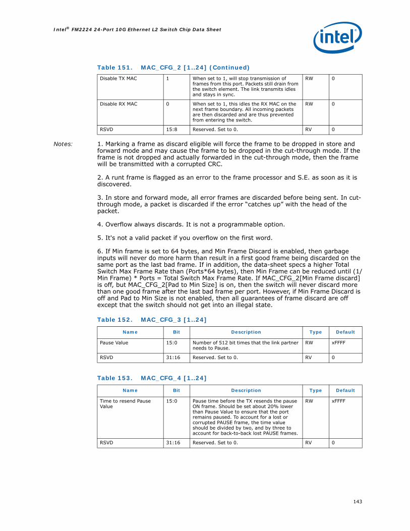
143
Intel® FM2224 24-Port 10G Ethernet L2 Switch Chip Data Sheet
Notes: 1. Marking a frame as discard eligible will force the frame to be dropped in store and forward mode and may cause the frame to be dropped in the cut-through mode. If the frame is not dropped and actually forwarded in the cut-through mode, then the frame will be transmitted with a corrupted CRC.
2. A runt frame is flagged as an error to the frame processor and S.E. as soon as it is discovered.
3. In store and forward mode, all error frames are discarded before being sent. In cut-through mode, a packet is discarded if the error “catches up” with the head of the packet.
4. Overflow always discards. It is not a programmable option.
5. It's not a valid packet if you overflow on the first word.
6. If Min frame is set to 64 bytes, and Min Frame Discard is enabled, then garbage inputs will never do more harm than result in a first good frame being discarded on the same port as the last bad frame. If in addition, the data-sheet specs a higher Total Switch Max Frame Rate than (Ports*64 bytes), then Min Frame can be reduced until (1/Min Frame) * Ports = Total Switch Max Frame Rate. If MAC_CFG_2[Min Frame discard] is off, but MAC_CFG_2[Pad to Min Size] is on, then the switch will never discard more than one good frame after the last bad frame per port. However, if Min Frame Discard is off and Pad to Min Size is not enabled, then all guarantees of frame discard are off except that the switch should not get into an illegal state.
Disable TX MAC 1 When set to 1, will stop transmission of frames from this port. Packets still drain from the switch element. The link transmits idles and stays in sync.
RW 0
Disable RX MAC 0 When set to 1, this idles the RX MAC on the next frame boundary. All incoming packets are then discarded and are thus prevented from entering the switch.
RW 0
RSVD 15:8 Reserved. Set to 0. RV 0
Table 152. MAC_CFG_3 [1..24]
Name Bit Description Type Default
Pause Value 15:0 Number of 512 bit times that the link partner needs to Pause.
RW xFFFF
RSVD 31:16 Reserved. Set to 0. RV 0
Table 153. MAC_CFG_4 [1..24]
Name Bit Description Type Default
Time to resend Pause Value
15:0 Pause time before the TX resends the pause ON frame. Should be set about 20% lower than Pause Value to ensure that the port remains paused. To account for a lost or corrupted PAUSE frame, the time value should be divided by two, and by three to account for back-to-back lost PAUSE frames.
RW xFFFF
RSVD 31:16 Reserved. Set to 0. RV 0
Table 151. MAC_CFG_2 [1..24] (Continued)

Intel® FM2224 24-Port 10G Ethernet L2 Switch Chip Data Sheet
144
Table 154. MAC_CFG_5 [1..24]
Name Bit Description Type Default
MSB of MA 15:0 Most significant 16 bits of the MAC address. Used as a source address when a PAUSE frame is transmitted.
RW 0
RSVD 31:16 Reserved. Set to 0. RV 0
Table 155. MAC_CFG_6 [1..24]
Name Bit Description Type Default
LSB of MA 31:0 Least significant 32 bits of the MAC address. Used as a source address when a PAUSE frame is transmitted.
RW 0
Table 156. TX_PRI_MAP_1 [1..24]
Name Bit Description Type Default
Pri7 Regen 31 Indicates if the Egress Priority shall be replace (1) or not (0) for switch priority 7.
RW 0x0
Pri7 30:28 Map Switch Priority 7 to Egress Priority RW 0x7
Pri6 Regen 27 Indicates if the Egress Priority shall be replace (1) or not (0) for switch priority 6.
RW 0x0
Pri6 26:24 Map Switch Priority 6 to Egress Priority RW 0x6
Pri5 Regen 23 Indicates if the Egress Priority shall be replace (1) or not (0) for switch priority 5.
RW 0x0
Pri5 22:20 Map Switch Priority 5 to Egress Priority RW 0x5
Pri4 Regen 19 Indicates if the Egress Priority shall be replace (1) or not (0) for switch priority 4.
RW 0x0
Pri4 18:16 Map Switch Priority 4 to Egress Priority RW 0x4
Pri3 Regen 15 Indicates if the Egress Priority shall be replace (1) or not (0) for switch priority 3.
RW 0x0
Pri3 14:12 Map Switch Priority 3 to Egress Priority RW 0x3
Pri2 Regen 11 Indicates if the Egress Priority shall be replace (1) or not (0) for switch priority 2.
RW 0x0
Pri2 10:8 Map Switch Priority 2 to Egress Priority RW 0x2
Pri1 Regen 7 Indicates if the Egress Priority shall be replace (1) or not (0) for switch priority 1.
RW 0x0
Pri1 6:4 Map Switch Priority 1 to Egress Priority RW 0x1
Pri0 Regen 3 Indicates if the Egress Priority shall be replace (1) or not (0) for switch priority 0.
RW 0x0
Pri0 2:0 Map Switch Priority 0 to Egress Priority RW 0x0
Table 157. TX_PRI_MAP_2 [1..24]
Name Bit Description Type Default
Pri15 Regen 31 Indicates if the Egress Priority shall be replace (1) or not (0) for switch priority 15.
RW 0x0
Pri15 30:28 Map Switch Priority 15 to Egress Priority RW 0x7

145
Intel® FM2224 24-Port 10G Ethernet L2 Switch Chip Data Sheet
Pri14 Regen 27 Indicates if the Egress Priority shall be replace (1) or not (0) for switch priority 14.
RW 0x0
Pri14 26:24 Map Switch Priority 14 to Egress Priority RW 0x6
Pri13 Regen 23 Indicates if the Egress Priority shall be replace (1) or not (0) for switch priority 13.
RW 0x0
Pri13 22:20 Map Switch Priority 13 to Egress Priority RW 0x5
Pri12 Regen 19 Indicates if the Egress Priority shall be replace (1) or not (0) for switch priority 12.
RW 0x0
Pri12 18:16 Map Switch Priority 12 to Egress Priority RW 0x4
Pri11 Regen 15 Indicates if the Egress Priority shall be replace (1) or not (0) for switch priority 11.
RW 0x0
Pri11 14:12 Map Switch Priority 11 to Egress Priority RW 0x3
Pri10 Regen 11 Indicates if the Egress Priority shall be replace (1) or not (0) for switch priority 10.
RW 0x0
Pri10 10:8 Map Switch Priority 10 to Egress Priority RW 0x2
Pri9 Regen 7 Indicates if the Egress Priority shall be replace (1) or not (0) for switch priority 9.
RW 0x0
Pri9 6:4 Map Switch Priority 9 to Egress Priority RW 0x1
Pri8 Regen 3 Indicates if the Egress Priority shall be replace (1) or not (0) for switch priority 8.
RW 0x0
Pri8 2:0 Map Switch Priority 8 to Egress Priority RW 0x0
Table 158. MAC_STATUS [1..24]
Name Bit Description Type Default
TX Status 1 TX idle RO 0
RX Status 0 RX idle RO 0
RSVD 31:2 Reserved. Set to 0. RV 0
Table 159. MAC_IP [1..24]
Name Bit Description Type Default
FE 10 Fabric error.This bit is set whenever the enable signal from the switch array becomes deasserted regardless where we are in the frame or if there is any data received at all.This could only happen if the crossbar becomes congested. It is not expected to happen if the chip is operated in normal conditions.
CR 0
PE 9 RX Pause Enable de-asserted (for debug purposes – should not be observed in normal operation)
CR 0
TU 8 TX underflow CR 0
TR 7 TX CRC without RX CRC error CR 0
TC 6 TX CRC error (inclusive of TR) CR 0
HE 5 RX PHY error CR 0
Table 157. TX_PRI_MAP_2 [1..24] (Continued)

Intel® FM2224 24-Port 10G Ethernet L2 Switch Chip Data Sheet
146
Note: The MAC and SERDES and PCS IP registers are or'd together to form a hardware EPL interrupt. This is visible at the per-port level interrupts.
Note: This register is made clear on read for the LED state machine. It is possible for the CPU to read this as well, in which case the results are cleared independent of the LED state machine. These fields are not “Or-d” into a standard interrupt detect chain.
PO 4 RX Pause Overflow.Note that this is for debug purpose at the unit level and cannot happen at the system level.
CR 0
JE 3 RX Oversized error CR 0
CE 2 RX CRC error CR 0
OE 1 Overflow error.This bit is set if a data word has been discarded because either the fabric or the frame control back pressured and data was actually lost.This could only happen once per frame.
CR 0
RE 0 RX Runt error CR 0
RSVD 31:11 Reserved. Set to 0. RV 0
Table 160. MAC_IM [1..24]
Name Bit Description Type Default
Mask Interrupts 10:0 For each interrupt:1 – Mask Interrupt0 – Do not mask interrupt
RW 0x7FF
RSVD 31:11 Reserved. Set to 0. RV 0
Table 161. EPL_INT_DETECT [1..24]
Name Bit Description Type Default
EPL_IP_3 2 There is an interrupt in MAC_IP RO 0
EPL_IP_2 1 There is an interrupt in PCS_IP RO 0
EPL_IP_1 0 There is an interrupt in SERDSE_IP RO 0
RSVD 31:3 Reserved. Set to 0. RV 0
Table 162. EPL_LED_STATUS [1..24]
Name Bit Description Type Default
TT 4 TX Port Transmitting – TX port transmiting data
CR 0
RR 3 RX Port Receiving – RX port receiving data CR 0
RL 2 RX Port Status – RX port has link up CR 0
PR 1 Port Remote Fault – port has or has sent a remote fault
CR 0
PS 0 Port Status - port has link sync error or no signal
CR 0
RSVD 31:5 Reserved. Set to 0. RV 0
Table 159. MAC_IP [1..24] (Continued)

147
Intel® FM2224 24-Port 10G Ethernet L2 Switch Chip Data Sheet
Table 163. STAT_EPL_ERROR1[1..24]
Name Bit Description Type Default
Overflow Count 15:8 Number of overflowed frames (RX) that were discarded before any information was sent to the FCU
RO 0
Underflow Count 7:0 Number of frame that were terminated early or discarded due to underflow in the TX
RO 0
RSVD 31:16 Reserved. Set to 0. RV 0
Table 164. STAT_EPL_ERROR2[1..24]
Name Bit Description Type Default
Corrupted Frame Count 15:0 Count the number of frames that where received with good CRC but transmitted with a bad CRC by this port because there was an error detected in the message array memory.
RO 0
RSVD 31:16 Reserved. Set to 0. RV 0
Table 165. STAT_RX_JABBER [1..24]
Name Bit Description Type Default
Jabber Count 15:0 Number of frames received in which frame size > MaxFrame and the CRC is invalid. Writing into this register will reset the register to 0.
RWC 0
RSVD 31:16 Reserved. Set to 0. RV 0
Table 166. STAT_TX_CRC [1..24]
Name Bit Description Type Default
TX CRC Errors 31:0 Number of frames transmitted with CRC errors. Part of the RMON counters, even though they are physically located in the MAC. Writing into this register will reset the register to 0.
RWC 0
Table 167. STAT_TX_PAUSE [1..24]
Name Bit Description Type Default
TX Pause 31:0 Number of Pause frames transmitted by the MAC. Part of the RMON counters, even though they are physically located in the MAC. Writing into this register will reset the register to 0.
RWC 0
Table 168. STAT_TX_BYTECOUNT [1..24]
Name Bit Description Type Default
TX Byte Count 63:0 Number of bytes transmitted (see STAT_TxOctets in the statistics section). Writing into this register will reset the register to 0.
RWC 0

Intel® FM2224 24-Port 10G Ethernet L2 Switch Chip Data Sheet
148
5.7.4 Scan Registers
Table 169. SCAN_FREQ_MULT
Name Bit Description Type Default
MGMT2SCAN 7:0 CLK_CPU divider RW 0
RSVD 31:8 Reserved. Set to 0. RV 0
Table 170. SCAN_CTRL
Name Bit Description Type Default
Shift Count 6:2 Number of bits to shift RW 0
Test Mode 1 Select group of scan chain:0 = scan chains 0-151 = scan chains 16-31
RW 0
Enable Capture 0 Execute capture (self clear after capture done)
RW 0
RSVD 31:7 Reserved. Set to 0. RV 0
Table 171. SCAN_SEL
Name Bit Description Type Default
Select 31:0 Select scan chain. This is a one hot encoding (1 << “n”).
RW 0
Table 172. SCAN_DATA_IN
Name Bit Description Type Default
Data 31:0 Data received from scan chain RO 0
Table 173. SCAN_DATA_OUT
Name Bit Description Type Default
Data 31:0 Data sent to scan chain RW 0

149
Intel® FM2224 24-Port 10G Ethernet L2 Switch Chip Data Sheet
6.0 Signal, Ball, and Package Descriptions
6.1 Package Overview
The FM2224 uses the following package:• Overall package dimensions of 40mm x 40mm• Flip-chip-based BGA package, with attached heat spreader• 39 balls on a side (ball pitch of 1.0mm)• 1,433 total balls in use
6.2 Power Mapping
The following figure shows a visual mapping of the power pins for the device:

Intel® FM2224 24-Port 10G Ethernet L2 Switch Chip Data Sheet
150
Figure 32. Power Mapping for the FM2224 1433-ball BGA Package (bottom view)
Note: Consult the FM2224 Design and Layout Guide (Intel® document number: FM2224-DG) for specific information on filtering strategies.
6.3 Interface Mapping
The following figure shows a visual mapping of the interface pins for the device:

151
Intel® FM2224 24-Port 10G Ethernet L2 Switch Chip Data Sheet
Figure 33. Interface Mapping (bottom view)
6.4 Signal Descriptions
This section describes the signals for the device, providing details on the name, ball assignment, type, and use of each signal.

Intel® FM2224 24-Port 10G Ethernet L2 Switch Chip Data Sheet
152
6.4.1 FM2224 Signals
Note: There are twenty-four XAUI interfaces in total. The “nn” in the above signal names represent a port number from 1 to 24.
Table 174. FM2224 XAUI Signal Pins
Signal Name I/O Type Description
Pnn_RAN [1:24] CML Input Differential receive inputs for channel A -- Complement
Pnn_RAP [1:24] CML Input Differential receive inputs for channel A -- True
Pnn_RBN [1:24] CML Input Differential receive inputs for channel B -- Complement
Pnn_RBP [1:24] CML Input Differential receive inputs for channel B -- True
Pnn_RCN [1:24] CML Input Differential receive inputs for channel C -- Complement
Pnn_RCP [1:24] CML Input Differential receive inputs for channel C -- True
Pnn_RDN [1:24] CML Input Differential receive inputs for channel C -- Complement
Pnn_RDP [1:24] CML Input Differential receive inputs for channel C -- True
Pnn_TAN [1:24] CML Output Differential transmit outputs for channel A - Complement
Pnn_TAP [1:24] CML Output Differential transmit outputs for channel A - True
Pnn_TBN [1:24] CML Output Differential transmit outputs for channel B - Complement
Pnn_TBP [1:24] CML Output Differential transmit outputs for channel B - True
Pnn_TCN [1:24] CML Output Differential transmit outputs for channel C - Complement
Pnn_TCP [1:24] CML Output Differential transmit outputs for channel C - True
Pnn_TDN [1:24] CML Output Differential transmit outputs for channel D - Complement
Pnn_TDP [1:24] CML Output Differential transmit outputs for channel D - True
RREF [1:24] Analog Ref-erence Reference resistor pad. RREF connects a 1.2KΩ external resistor to VDDA to provide a reference current for the driver and equalization circuits
Table 175. FM2224 High-Speed Clock Signal Pins
Signal Name I/O Type Description
RCK1AN CML (1)LVDSLVPECL
Input Differential Reference Clock A for Ports 1, 3, 5, 7, 9, 11Complement
RCK1AP CML (1)LVDSLVPECL
Input Differential Reference Clock A for Ports 1, 3, 5, 7, 9, 11True
RCK1BN CML (1)LVDSLVPECL
Input Differential Reference Clock B for Ports 1, 3, 5, 7, 9, 11Complement

153
Intel® FM2224 24-Port 10G Ethernet L2 Switch Chip Data Sheet
Note: These pins are AC coupled and are compatible with the stated IO. For LVDS IO a 2K resistor is required between the lines on the driver side of the isolation capacitors
RCK1BP CML (1)LVDSLVPECL
Input Differential Reference Clock B for Ports 1, 3, 5, 7, 9, 11True
RCK2AN CML (1)LVDSLVPECL
Input Differential Reference Clock A for Ports 2, 4, 6, 8, 10, 12Complement
RCK2AP CML (1)LVDSLVPECL
Input Differential Reference Clock A for Ports 2, 4, 6, 8, 10, 12 True
RCK2BN CML (1)LVDSLVPECL
Input Differential Reference Clock B for Ports 2, 4, 6, 8, 10, 12 Complement
RCK2BP CML (1)LVDSLVPECL
Input Differential Reference Clock B for Ports 2, 4, 6, 8, 10, 12 True
RCK3AN CML (1)LVDSLVPECL
Input Differential Reference ClockA for Ports 13, 15, 17, 19, 21, 23Complement
RCK3AP CML (1)LVDSLVPECL
Input Differential Reference ClockA for Ports 13, 15, 17, 19, 21, 23True
RCK3BN CML (1)LVDSLVPECL
Input Differential Reference ClockB for Ports 13, 15, 17, 19, 21, 23Complement
RCK3BP CML (1)LVDSLVPECL
Input Differential Reference ClockB for Ports 13, 15, 17, 19, 21, 23True
RCK4AN CML (1)LVDSLVPECL
Input Differential Reference Clock A for Ports 14, 16, 18, 20, 22, 24Complement
RCK4AP CML (1)LVDSLVPECL
Input Differential Reference Clock A for Ports 14, 16, 18, 20, 22, 24True
RCK4BN CML (1)LVDSLVPECL
Input Differential Reference Clock B for Ports 14, 16, 18, 20, 22, 24Complement
RCK4BP CML (1)LVDSLVPECL
Input Differential Reference Clock B for Ports 14, 16, 18, 20, 22, 24True
Table 175. FM2224 High-Speed Clock Signal Pins (Continued)

Intel® FM2224 24-Port 10G Ethernet L2 Switch Chip Data Sheet
154
Table 176. FM2224 CPU Interface Signal Pins
Signal Name I/O Type Description
CPU_CLK Input LVTTL Clock for Bus Interface (maximum frequency is 100MHz)
CS_N Input LVTTL Chip select. Active low. Enables the FM2224 to act on an incoming request. Allows multiple devices with the same address space to share the bus. Two uses for the signal: (1) To enable the start of a new request – to qualify AS_N; (2) To qualify the outputs DATA and DTACK_N. When asserted, the two outputs are tri-stated. (Pull-up recommended on board.)
ADDR[23:2] Input LVTTL Address Bus. Address must be driven whenever AS_N asserted.
DATA[31:0] In/Out LVTTL Bi-directional data bus. Must be driven when AS_N and RW_N (read) are asserted. Will be driven on a write when DTACK_N is asserted. The DATA bus is undriven when the device is coming out of reset. (Pull-down recommended on board.)
PAR[3:0] In/Out LVTTL Even parity for each byte of data. PAR must be driven when AS_N and RM_N (read) are asserted and Ignore_Parity strapping pin is not asserted. PAR will be driven on a write when DTACK_N is asserted. (Pull-down recommended on board.)
AS_N Input LVTTL Address Strobe. Indicates the start of a valid transaction on the bus. Active Low. Must be inactive after reset. (Pull-up recommended on board.)
RW_N Input LVTTL Read/Write. Indicates when a read (active high) or write (active low) transaction is being requested. Determines which device drives the data bus. Polarity can be switched through the RW_INV strapping pin.
RW_INV Input LVTTL Inverts RW_N pin. When connected to ground, then read is active high while write is active low. Conversely, when connected to VDD33, read is active low while write is active high.
DTACK_N Output LVTTL Data transfer acknowledge. Indicates the completion of a data transfer. At the termination of a request, this signal is actively driven inactive for 1 cycle and then tri-stated. The pin is tri-stated when the device is coming out of reset. Pull-up or pull-down should be added to board, according to whether DTACK_INV is asserted.
DTACK_INV Input LVTTL Strap pin. Inverts sense of DTACK_N. If connected to ground, then DTACK_N is active low. If connected to VDD33, then DTACK_N is active high.
DERR_N Output LVTTL Data error occurred; transaction must be aborted and was not completed. Indicates write data parity errors. Only asserted (and valid) when DTACK_N asserted. Tri-stated otherwise.
CPU_RESET_N Input LVTTL Hard reset for Management block domain. Reserved for Intel®. Connect to an external pull-up.
INTR_N Output SE, Open Drain
Synchronous interrupt. Indicates an internal error. The global interrupt status register must be checked to ascertain the source of the problem. Active Low. (Pull-up recommended on board.)
IGNORE_PARITY Input LVTTL Disables parity checking on incoming write data.

155
Intel® FM2224 24-Port 10G Ethernet L2 Switch Chip Data Sheet
Table 177. FM2224 DMA Pins
Signal Name I/O Type Description
TXRDY_N Output LVTTL Transmit queue is ready to receive (connected to Pause channel)
RXRDY_N Output LVTTL Receive queue has data to send to CPU
RXEOUT Output LVTTL End of frame indication (instructs DMA controller to begin storing data to a new frame descriptor)
Table 178. FM2224 SPI Interface Signal Pins
Signal Name I/O Type Description
SPI_CLK Output LVTTL SPI clock
SPI_CS_N Output LVTTL SPI chip select (active low)
SPI_SI Input LVTTL Serial data input
SPI_SO Output LVTTL Serial data output
Table 179. FM2224 LED Interface Signal Pins
Signal Name I/O Type Description
LED_CLK Output LVTTL Provides a continuous clock synchronous to the serial data stream output on the LED_DATA pin. Tri-stated with LED_EN.
LED_DATA0 Output LVTTL Serial bit stream from ports 1-8, and 0. Ports 1-8 are driven first, and then the CPU port (port 0) is driven. Asserted on the negative edge of LED_CLK. Tri-stated with LED_EN.
LED_DATA1 Output LVTTL Serial bit stream from ports 9-16. Data is driven on the negative edge of LED_CLK and is valid on the rising edge of CLK_LED. Mode 1 inverts the polarity of the data. Tri-stated with LED_EN.
LED_DATA2 Output LVTTL Serial bit stream from ports 17-24. Data is driven on the negative edge of LED_CLK and is valid on the rising edge of CLK_LED. Mode 1 inverts the polarity of the data. Tri-stated with LED_EN.
LED_EN Output LVTTL Used in Mode1 as the latch enable for the shift register chain. In Mode 0, this signal is not used and should be left unconnected. Asserted when LED_CLK is low, coincident with the 36th bit (last bit in LED data stream). Tri-stated with LED_EN.
Table 180. FM2224 JTAG Interface Signal Pins
Signal Name I/O Type Description
TCK Input LVTTL JTAG Clock
TDI Input LVTTL JTAG Input Data. Internally pulled up.
TMS Input LVTTL JTAG Test Mode. Internally pulled up.
TRST_N Input LVTTL JTAG Reset Pin. Internally pulled up.
TDO Output LVTTL JTAG Data Out

Intel® FM2224 24-Port 10G Ethernet L2 Switch Chip Data Sheet
156
Note: When not using the JTAG interface, either drive the TCK pin with an external clock, or drive the TRST_N pin low. Conversely, when using the JTAG interface assert TRST_N along with chip reset to ensure proper reset of the JTAG interface prior to use.
Table 181. FM2224 Miscellaneous Signal Pins
Signal Name I/O Type Description
CHIP_RESET_N Input LVTTL Hard reset for the entire chip.
CONT_EN Input LVTTL SerDes continuity test enable.
CONT_OUT Output LVTTL SerDes continuity test output.
DIODE_INDIODE_OUT
Sense LVTTL Die temperature is measured with a standard temperature sensing diode. Both terminals of the diode are exposed through the die to the package.
EEPROM_EN Input LVTTL EEPROM enable. Enabled when high. Pull low to bypass EEPROM and boot from processor.
AUTOBOOT Input LVTTL When asserted, the BOOT FSM starts automatically after RESET is de-asserted, initializing the chip according to the content of fusebox. Returns control to the CPU Interface after the initialization is completed. Pull low to boot from processor
FH_PLL_REFCLK Input LVTTL Refclock input to frame handler PLL
FH_PLL_CLKOUT Output Reserved for Intel® use and should be left unconnected
TESTMODE Input Reserved for Intel® use. Must be pulled down in normal operation.

157
Intel® FM2224 24-Port 10G Ethernet L2 Switch Chip Data Sheet
6.4.2 Power Supply Pins and Recommendations
6.4.3 Recommended Connections
Ideally the following power supplies should be on the board containing the FM2224:
• A 1.2 V source to supply the core (VDD)• A 1.2 V or 1.0 V source to supply power to the SerDes (VDDX)
Table 182. List of no connects and unpopulated ball locations
Pins Description
ag15, ag16, ag17, ag18, ag19, ag20, ag21, ag22, ag23, ag24, ag25ah15, ah16, ah17, ah18, ah19,ah20, ah21, ah22, ah23, ah24, ah25m15, m16, m17, m18, m19, m20, m21,m 22, m23,m 24, m25n15, n16, n17, n18, n19, n20,n 21, n22, n23, n24, n25r12,r13, r27, r28t12, t13, t27, t28u12,u13, u27,u 28v12, v13,v 27, v28w12, w13, w27, w28y12, y13, y27, y28aa12, aa13, aa27, aa28ab12, ab13, ab27, ab28ac12,ac13, ac27, ac28ad12,ad13, ad27, ad28ae12,ae13, ae27, ae28
Ball grid locations that are not populated with solder balls
p32, p33ag30, ag31, ag32, ag33r30, r32, r33, r38, r39t30v31, v32w32y32aa32ab31, ab32n30af29, af31, af32, af33
No connects
Table 183. FM2224 Power Supply Signal Descriptions
Signal Name Quantity Type Description
VSS 448 Power Ground, for Core and I/O
VDD 179 Power Core VDD (1.2 V)
VDD33 12 Power I/O VDD (3.3 V), for LVTTL
VDDA33 1 Power PLL analog supply
VDDA 24 Power SerDes bias voltage
VDDX 128 Power SerDes supply voltage
VTT 96 Power TX termination voltage, which can be used to adjust the common mode voltage and swing of TX outputs

Intel® FM2224 24-Port 10G Ethernet L2 Switch Chip Data Sheet
158
• A 1.2 V source to supply bias to the SerDes (VDDA)• A 1.5 V typical source to terminate and set the common mode of the CML TX
interface (VTT)• A 3.3 V supply for the LVTTL I/O signals (VDD33)• A 3.3 V noise minimized source to supply the PLL (VDDA33)
6.4.3.1 Recommended Filtering
The power supply should be filtered both at the source of the power supply and local to the power supply balls on the FM2224. The power balls have been designed to take advantage of the space on the inside of the signal pins on the back side of the board for this purpose.
Note: Consult the FM2224 Design and Layout Guide (Intel® document number: FM2224 DG) for specific information on filtering strategies.
6.4.3.2 Power Supply Sequencing
The FM2224 TTL I/Os use the 3.3V supply, but the internal logic in the switch contolling those I/Os uses the VDD supply. If the 3.3V is present on the part and the VDD is not, then the I/Os are in an unpredictable state. As an example, if a processor is attached to the FM2224 via the CPU bus and to a boot ROM on the same bus, then the fact that the FM2224 I/Os could be in an unknown state (if VDD is not present) may cause a boot problem. To solve this problem, ensure that VDD is applied before a general master reset is de-asserted to the main processor as this will ensure that the TTL I/Os are in a correct state. Another way to solve this problem would be to use tri-state buffers on the EBI bus.
The correct power sequencing is:• Apply power to all components, including the switch• De-assert master reset on board• Optional de-assert reset on the switch (but not required at this stage)• Processor boots (if processor present)• Processor de-assert reset on the switch (if not done)
— EBI clock must be present on the switch before the reset is deasserted (10 cycles good enough).
6.4.4 Ball Assignment
Table 184. Package Ball Assignment in Numerical Order
Pkg Ball Signal Name Pkg
Ball Signal Name Pkg Ball Signal Name
a1 P20_TDP p1 VSS ag1 P23_TDP
a2 VSS p2 VTT24 ag2 P23_TDN
a3 P20_TCP p3 VDDX ag3 VSS

159
Intel® FM2224 24-Port 10G Ethernet L2 Switch Chip Data Sheet
a4 VSS p4 VTT24 ag4 P23_RDP
a5 P20_TBP p5 VSS ag5 P23_RDN
a6 VSS p6 VDD ag6 VDD
a7 P20_TAP p7 VSS ag7 P17_TDP
a8 VSS p8 VTT18 ag8 P17_TDN
a9 P14_TDP p9 VDDX ag9 VSS
a10 VSS p10 VTT18 ag10 P17_RDP
a11 P14_TCP p11 VSS ag11 P17_RDN
a12 VSS p12 VDDX ag12 VDDX
a13 P14_TBP p13 RCK4AN ag13 RCK3AN
a14 VSS p14 RCK4BN ag14 RCK3BN
a15 P14_TAP p15 VSS ag15 NO BALL
a16 VSS p16 VSS ag16 NO BALL
a17 P12_TDP p17 VDD ag17 NO BALL
a18 VSS p18 VDD ag18 NO BALL
a19 P12_TCP p19 VSS ag19 NO BALL
a20 VSS p20 VSS ag20 NO BALL
a21 P12_TBP p21 VSS ag21 NO BALL
a22 VSS p22 VDD ag22 NO BALL
a23 P12_TAP p23 VDD ag23 NO BALL
a24 VSS p24 VSS ag24 NO BALL
a25 P08_TDP p25 VSS ag25 NO BALL
a26 VSS p26 RCK2BN ag26 RCK1BN
a27 P08_TCP p27 RCK2AN ag27 RCK1AN
a28 VSS p28 VDDX ag28 VDDX
a29 P08_TBP p29 LEDCLK ag29 VSS
a30 VSS p30 NC ag30 NC
a31 P08_TAP p31 CONT_OUT ag31 NC
a32 VSS p32 NC ag32 NC
a33 P04_TDP p33 NC ag33 NC
a34 VSS p34 VSS ag34 VSS
a35 P04_TCP p35 VSS ag35 P01_RDN
a36 VSS p36 VSS ag36 P01_RDP
a37 P04_TBP p37 VSS ag37 VSS
a38 VSS p38 VSS ag38 P01_TDN
a39 P04_TAP p39 VSS ag39 P01_TDP
b1 P20_TDN r1 P24_TBP ah1 VSS
b2 VTT20 r2 P24_TBN ah2 VSS
b3 P20_TCN r3 VDDX ah3 VSS
b4 VDDX r4 P24_RBP ah4 VDD
b5 P20_TBN r5 P24_RBN ah5 VDD
b6 VTT20 r6 VSS ah6 VDD
Table 184. Package Ball Assignment in Numerical Order (Continued)

Intel® FM2224 24-Port 10G Ethernet L2 Switch Chip Data Sheet
160
b7 P20_TAN r7 P18_TBP ah7 VDD
b8 VSS r8 P18_TBN ah8 VDD
b9 P14_TDN r9 VDDX ah9 VDD
b10 VTT14 r10 P18_RBP ah10 VDD
b11 P14_TCN r11 P18_RBN ah11 VDD
b12 VDDX r12 NO BALL ah12 VSS
b13 P14_TBN r13 NO BALL ah13 VSS
b14 VTT14 r14 VSS ah14 VSS
b15 P14_TAN r15 VSS ah15 NO BALL
b16 VSS r16 VSS ah16 NO BALL
b17 P12_TDN r17 VDD ah17 NO BALL
b18 VTT12 r18 VDD ah18 NO BALL
b19 P12_TCN r19 VSS ah19 NO BALL
b20 VDDX r20 VSS ah20 NO BALL
b21 P12_TBN r21 VSS ah21 NO BALL
b22 VTT12 r22 VDD ah22 NO BALL
b23 P12_TAN r23 VDD ah23 NO BALL
b24 VSS r24 VSS ah24 NO BALL
b25 P08_TDN r25 VSS ah25 NO BALL
b26 VTT08 r26 VSS ah26 VSS
b27 P08_TCN r27 NO BALL ah27 VSS
b28 VDDX r28 NO BALL ah28 VSS
b29 P08_TBN r29 LED_DATA0 ah29 VSS
b30 VTT08 r30 NC ah30 VSS
b31 P08_TAN r31 EEPROM_EN ah31 VSS
b32 VSS r32 NC ah32 VSS
b33 P04_TDN r33 NC ah33 DIODE_IN
b34 VTT04 r34 SPI_SO ah34 VSS
b35 P04_TCN r35 SPI_CS_N ah35 VSS
b36 VDDX r36 SPI_SCK ah36 VTT01
b37 P04_TBN r37 SPI_SI ah37 VDDX
b38 VTT04 r38 NC ah38 VTT01
b39 P04_TAN r39 NC ah39 VSS
c1 VSS t1 VSS aj1 P21_RAN
c2 VDDX t2 VDDX aj2 VSS
c3 VDDX t3 VDDA aj3 P21_RBN
c4 VDDA t4 RREF24 aj4 VSS
c5 VDDX t5 VSS aj5 P21_RCN
c6 VDDX t6 VSS aj6 VSS
c7 VSS t7 VSS aj7 P21_RDN
c8 VSS t8 VDDX aj8 VDD
c9 VSS t9 VDDA aj9 P15_RAN
Table 184. Package Ball Assignment in Numerical Order (Continued)

161
Intel® FM2224 24-Port 10G Ethernet L2 Switch Chip Data Sheet
c10 VDDX t10 RREF18 aj10 VSS
c11 VDDX t11 VSS aj11 P15_RBN
c12 VDDA t12 NO BALL aj12 VSS
c13 VDDX t13 NO BALL aj13 P15_RCN
c14 VDDX t14 VDD aj14 VSS
c15 VSS t15 VDD aj15 P15_RDN
c16 VSS t16 VDD aj16 VDD
c17 VSS t17 VDD aj17 P09_RAN
c18 VDDX t18 VDD aj18 VSS
c19 VDDX t19 VDD aj19 P09_RBN
c20 VDDA t20 VDD aj20 VSS
c21 VDDX t21 VDD aj21 P09_RCN
c22 VDDX t22 VDD aj22 VSS
c23 VSS t23 VDD aj23 P09_RDN
c24 VSS t24 VDD aj24 VDD
c25 VSS t25 VDD aj25 P05_RAN
c26 VDDX t26 VDD aj26 VSS
c27 VDDX t27 NO BALL aj27 P05_RBN
c28 VDDA t28 NO BALL aj28 VSS
c29 VDDX t29 LED_DATA1 aj29 P05_RCN
c30 VDDX t30 NC aj30 VSS
c31 VSS t31 TESTMODE aj31 P05_RDN
c32 VSS t32 ADDR[2] aj32 VDD
c33 VSS t33 ADDR[3] aj33 DIODE_OUT
c34 VDDX t34 ADDR[4] aj34 VDD
c35 VDDX t35 ADDR[5] aj35 P01_RCN
c36 VDDA t36 ADDR[6] aj36 P01_RCP
c37 VDDX t37 ADDR[7] aj37 VDDX
c38 VDDX t38 ADDR[8] aj38 P01_TCN
c39 VSS t39 ADDR[9] aj39 P01_TCP
d1 P20_RDP u1 P24_TCP ak1 P21_RAP
d2 VTT20 u2 P24_TCN ak2 VTT21
d3 P20_RCP u3 VDDX ak3 P21_RBP
d4 RREF20 u4 P24_RCP ak4 RREF21
d5 P20_RBP u5 P24_RCN ak5 P21_RCP
d6 VTT20 u6 VSS ak6 VTT21
d7 P20_RAP u7 P18_TCP ak7 P21_RDP
d8 VDD u8 P18_TCN ak8 VDD
d9 P14_RDP u9 VDDX ak9 P15_RAP
d10 VTT14 u10 P18_RCP ak10 VTT15
d11 P14_RCP u11 P18_RCN ak11 P15_RBP
d12 RREF14 u12 NO BALL ak12 RREF15
Table 184. Package Ball Assignment in Numerical Order (Continued)

Intel® FM2224 24-Port 10G Ethernet L2 Switch Chip Data Sheet
162
d13 P14_RBP u13 NO BALL ak13 P15_RCP
d14 VTT14 u14 VDD ak14 VTT15
d15 P14_RAP u15 VDD ak15 P15_RDP
d16 VDD u16 VDD ak16 VDD
d17 P12_RDP u17 VDD ak17 P09_RAP
d18 VTT12 u18 VDD ak18 VTT09
d19 P12_RCP u19 VDD ak19 P09_RBP
d20 RREF12 u20 VDD ak20 RREF09
d21 P12_RBP u21 VDD ak21 P09_RCP
d22 VTT12 u22 VDD ak22 VTT09
d23 P12_RAP u23 VDD ak23 P09_RDP
d24 VDD u24 VDD ak24 VDD
d25 P08_RDP u25 VDD ak25 P05_RAP
d26 VTT08 u26 VDD ak26 VTT05
d27 P08_RCP u27 NO BALL ak27 P05_RBP
d28 RREF08 u28 NO BALL ak28 RREF05
d29 P08_RBP u29 LED_DATA2 ak29 P05_RCP
d30 VTT08 u30 DTACK_N ak30 VTT05
d31 P08_RAP u31 ADDR[10] ak31 P05_RDP
d32 VDD u32 ADDR[11] ak32 VDD
d33 P04_RDP u33 ADDR[12] ak33 VSS
d34 VTT04 u34 ADDR[13] ak34 VDD
d35 P04_RCP u35 ADDR[14] ak35 VSS
d36 RREF04 u36 ADDR[15] ak36 RREF01
d37 P04_RBP u37 ADDR[16] ak37 VDDA
d38 VTT04 u38 ADDR[17] ak38 VDDX
d39 P04_RAP u39 ADDR[18] ak39 VSS
e1 P20_RDN v1 VSS al1 VSS
e2 VSS v2 VTT24 al2 VDDX
e3 P20_RCN v3 VDDX al3 VDDX
e4 VSS v4 VTT24 al4 VDDA
e5 P20_RBN v5 VSS al5 VDDX
e6 VSS v6 VSS al6 VDDX
e7 P20_RAN v7 VSS al7 VSS
e8 VDD v8 VTT18 al8 VSS
e9 P14_RDN v9 VDDX al9 VSS
e10 VSS v10 VTT18 al10 VDDX
e11 P14_RCN v11 VSS al11 VDDX
e12 VSS v12 NO BALL al12 VDDA
e13 P14_RBN v13 NO BALL al13 VDDX
e14 VSS v14 VSS al14 VDDX
e15 P14_RAN v15 VSS al15 VSS
Table 184. Package Ball Assignment in Numerical Order (Continued)

163
Intel® FM2224 24-Port 10G Ethernet L2 Switch Chip Data Sheet
e16 VDD v16 VSS al16 VSS
e17 P12_RDN v17 VSS al17 VSS
e18 VSS v18 VSS al18 VDDX
e19 P12_RCN v19 VSS al19 VDDX
e20 VSS v20 VSS al20 VDDA
e21 P12_RBN v21 VSS al21 VDDX
e22 VSS v22 VSS al22 VDDX
e23 P12_RAN v23 VSS al23 VSS
e24 VDD v24 VSS al24 VSS
e25 P08_RDN v25 VSS al25 VSS
e26 VSS v26 VSS al26 VDDX
e27 P08_RCN v27 NO BALL al27 VDDX
e28 VSS v28 NO BALL al28 VDDA
e29 P08_RBN v29 LED_EN al29 VDDX
e30 VSS v30 DERR_N al30 VDDX
e31 P08_RAN v31 NC al31 VSS
e32 VDD v32 NC al32 VSS
e33 P04_RDN v33 ADDR[19] al33 VSS
e34 VSS v34 ADDR[20] al34 VDD
e35 P04_RCN v35 ADDR[21] al35 P01_RBN
e36 VSS v36 ADDR[22] al36 P01_RBP
e37 P04_RBN v37 ADDR[23] al37 VDDX
e38 VSS v38 VSS al38 P01_TBN
e39 P04_RAN v39 VSS al39 P01_TBP
f1 VSS w1 P24_TDP am1 P21_TAN
f2 VSS w2 P24_TDN am2 VTT21
f3 VSS w3 VSS am3 P21_TBN
f4 VDD w4 P24_RDP am4 VDDX
f5 VDD w5 P24_RDN am5 P21_TCN
f6 VDD w6 VDD am6 VTT21
f7 VDD w7 P18_TDP am7 P21_TDN
f8 VDD w8 P18_TDN am8 VSS
f9 VDD w9 VSS am9 P15_TAN
f10 VSS w10 P18_RDP am10 VTT15
f11 VSS w11 P18_RDN am11 P15_TBN
f12 VSS w12 NO BALL am12 VDDX
f13 VSS w13 NO BALL am13 P15_TCN
f14 VSS w14 VSS am14 VTT15
f15 VDD w15 VSS am15 P15_TDN
f16 VDD w16 VSS am16 VSS
f17 VDD w17 VSS am17 P09_TAN
f18 VSS w18 VSS am18 VTT09
Table 184. Package Ball Assignment in Numerical Order (Continued)

Intel® FM2224 24-Port 10G Ethernet L2 Switch Chip Data Sheet
164
f19 VSS w19 VSS am19 P09_TBN
f20 VSS w20 VSS am20 VDDX
f21 VSS w21 VSS am21 P09_TCN
f22 VSS w22 VSS am22 VTT09
f23 VDD w23 VSS am23 P09_TDN
f24 VDD w24 VSS am24 VSS
f25 VDD w25 VDD33 am25 P05_TAN
f26 VSS w26 VDD33 am26 VTT05
f27 VSS w27 NO BALL am27 P05_TBN
f28 VSS w28 NO BALL am28 VDDX
f29 VSS w29 VSS am29 P05_TCN
f30 VSS w30 VSS am30 VTT05
f31 VDD w31 VSS am31 P05_TDN
f32 VDD w32 NC am32 VSS
f33 VDD w33 IGN_PAR am33 VSS
f34 VDD w34 CS_N am34 VDD
f35 VDD w35 AS_N am35 VSS
f36 VDD w36 INTR_N am36 VTT01
f37 VSS w37 AUTOBOOT am37 VDDX
f38 VSS w38 VDD33 am38 VTT01
f39 VSS w39 VDD33 am39 VSS
g1 P22_TDP y1 VSS an1 P21_TAP
g2 VSS y2 VSS an2 VSS
g3 P22_TCP y3 VSS an3 P21_TBP
g4 VSS y4 VDD an4 VSS
g5 P22_TBP y5 VDD an5 P21_TCP
g6 VSS y6 VDD an6 VSS
g7 P22_TAP y7 VSS an7 P21_TDP
g8 VSS y8 VSS an8 VSS
g9 P16_TDP y9 VSS an9 P15_TAP
g10 VSS y10 VSS an10 VSS
g11 P16_TCP y11 VSS an11 P15_TBP
g12 VSS y12 NO BALL an12 VSS
g13 P16_TBP y13 NO BALL an13 P15_TCP
g14 VSS y14 VDD an14 VSS
g15 P16_TAP y15 VDD an15 P15_TDP
g16 VSS y16 VDD an16 VSS
g17 P10_TDP y17 VDD an17 P09_TAP
g18 VSS y18 VDD an18 VSS
g19 P10_TCP y19 VSS an19 P09_TBP
g20 VSS y20 VSS an20 VSS
g21 P10_TBP y21 VSS an21 P09_TCP
Table 184. Package Ball Assignment in Numerical Order (Continued)

165
Intel® FM2224 24-Port 10G Ethernet L2 Switch Chip Data Sheet
g22 VSS y22 VDD an22 VSS
g23 P10_TAP y23 VDD an23 P09_TDP
g24 VSS y24 VDD an24 VSS
g25 P06_TDP y25 VDD33 an25 P05_TAP
g26 VSS y26 VDD33 an26 VSS
g27 P06_TCP y27 NO BALL an27 P05_TBP
g28 VSS y28 NO BALL an28 VSS
g29 P06_TBP y29 VSS an29 P05_TCP
g30 VSS y30 CPU_RESET_N an30 VSS
g31 P06_TAP y31 VSS an31 P05_TDP
g32 VSS y32 NC an32 VSS
g33 VSS y33 RXRDY an33 VSS
g34 VDD y34 TXRDY_N an34 VDD
g35 P02_RDN y35 RXEOT an35 P01_RAN
g36 P02_RDP y36 RW_N an36 P01_RAP
g37 VSS y37 CLK_CPU an37 VSS
g38 P02_TDN y38 VDD33 an38 P01_TAN
g39 P02_TDP y39 VDD33 an39 P01_TAP
h1 P22_TDN aa1 P23_TAP ap1 VSS
h2 VTT22 aa2 P23_TAN ap2 VSS
h3 P22_TCN aa3 VSS ap3 VSS
h4 VDDX aa4 P23_RAP ap4 VDD
h5 P22_TBN aa5 P23_RAN ap5 VDD
h6 VTT22 aa6 VDD ap6 VDD
h7 P22_TAN aa7 P17_TAP ap7 VDD
h8 VSS aa8 P17_TAN ap8 VDD
h9 P16_TDN aa9 VSS ap9 VDD
h10 VTT16 aa10 P17_RAP ap10 VSS
h11 P16_TCN aa11 P17_RAN ap11 VSS
h12 VDDX aa12 NO BALL ap12 VSS
h13 P16_TBN aa13 NO BALL ap13 VSS
h14 VTT16 aa14 VSS ap14 VSS
h15 P16_TAN aa15 VSS ap15 VDD
h16 VSS aa16 VSS ap16 VDD
h17 P10_TDN aa17 VSS ap17 VDD
h18 VTT10 aa18 VSS ap18 VSS
h19 P10_TCN aa19 VSS ap19 VSS
h20 VDDX aa20 VSS ap20 VSS
h21 P10_TBN aa21 VSS ap21 VSS
h22 VTT10 aa22 VSS ap22 VSS
h23 P10_TAN aa23 VSS ap23 VDD
h24 VSS aa24 VSS ap24 VDD
Table 184. Package Ball Assignment in Numerical Order (Continued)

Intel® FM2224 24-Port 10G Ethernet L2 Switch Chip Data Sheet
166
h25 P06_TDN aa25 VDD33 ap25 VDD
h26 VTT06 aa26 VDD33 ap26 VSS
h27 P06_TCN aa27 NO BALL ap27 VSS
h28 VDDX aa28 NO BALL ap28 VSS
h29 P06_TBN aa29 VSS ap29 VSS
h30 VTT06 aa30 VSS ap30 VSS
h31 P06_TAN aa31 VSS ap31 VDD
h32 VSS aa32 NC ap32 VDD
h33 VSS aa33 DTACK_INV ap33 VDD
h34 VDD aa34 PAR[0] ap34 VDD
h35 VSS aa35 PAR[1] ap35 VDD
h36 VTT02 aa36 PAR[2] ap36 VDD
h37 VDDX aa37 PAR[3] ap37 VSS
h38 VTT02 aa38 VDD33 ap38 VSS
h39 VSS aa39 VDD33 ap39 VSS
j1 VSS ab1 VSS ar1 P19_RAN
j2 VDDX ab2 VTT23 ar2 VSS
j3 VDDX ab3 VDDX ar3 P19_RBN
j4 VDDA ab4 VTT23 ar4 VSS
j5 VDDX ab5 VSS ar5 P19_RCN
j6 VDDX ab6 VSS ar6 VSS
j7 VSS ab7 VSS ar7 P19_RDN
j8 VSS ab8 VTT17 ar8 VDD
j9 VSS ab9 VDDX ar9 P13_RAN
j10 VDDX ab10 VTT17 ar10 VSS
j11 VDDX ab11 VSS ar11 P13_RBN
j12 VDDA ab12 NO BALL ar12 VSS
j13 VDDX ab13 NO BALL ar13 P13_RCN
j14 VDDX ab14 VSS ar14 VSS
j15 VSS ab15 VSS ar15 P13_RDN
j16 VSS ab16 VSS ar16 VDD
j17 VSS ab17 VSS ar17 P11_RAN
j18 VDDX ab18 VSS ar18 VSS
j19 VDDX ab19 VSS ar19 P11_RBN
j20 VDDA ab20 VSS ar20 VSS
j21 VDDX ab21 VSS ar21 P11_RCN
j22 VDDX ab22 VSS ar22 VSS
j23 VSS ab23 VSS ar23 P11_RDN
j24 VSS ab24 VSS ar24 VDD
j25 VSS ab25 VSS ar25 P07_RAN
j26 VDDX ab26 VSS ar26 VSS
j27 VDDX ab27 NO BALL ar27 P07_RBN
Table 184. Package Ball Assignment in Numerical Order (Continued)

167
Intel® FM2224 24-Port 10G Ethernet L2 Switch Chip Data Sheet
j28 VDDA ab28 NO BALL ar28 VSS
j29 VDDX ab29 VDDA33 ar29 P07_RCN
j30 VDDX ab30 TDI ar30 VSS
j31 VSS ab31 NC ar31 P07_RDN
j32 VSS ab32 NC ar32 VDD
j33 VSS ab33 DATA[0] ar33 P03_RAN
j34 VDD ab34 DATA[1] ar34 VSS
j35 P02_RCN ab35 DATA[2] ar35 P03_RBN
j36 P02_RCP ab36 DATA[3] ar36 VSS
j37 VDDX ab37 DATA[4] ar37 P03_RCN
j38 P02_TCN ab38 VSS ar38 VSS
j39 P02_TCP ab39 VSS ar39 P03_RDN
k1 P22_RDP ac1 P23_TBP at1 P19_RAP
k2 VTT22 ac2 P23_TBN at2 VTT19
k3 P22_RCP ac3 VDDX at3 P19_RBP
k4 RREF22 ac4 P23_RBP at4 RREF19
k5 P22_RBP ac5 P23_RBN at5 P19_RCP
k6 VTT22 ac6 VSS at6 VTT19
k7 P22_RAP ac7 P17_TBP at7 P19_RDP
k8 VDD ac8 P17_TBN at8 VDD
k9 P16_RDP ac9 VDDX at9 P13_RAP
k10 VTT16 ac10 P17_RBP at10 VTT13
k11 P16_RCP ac11 P17_RBN at11 P13_RBP
k12 RREF16 ac12 NO BALL at12 RREF13
k13 P16_RBP ac13 NO BALL at13 P13_RCP
k14 VTT16 ac14 VDD at14 VTT13
k15 P16_RAP ac15 VDD at15 P13_RDP
k16 VDD ac16 VDD at16 VDD
k17 P10_RDP ac17 VDD at17 P11_RAP
k18 VTT10 ac18 VDD at18 VTT11
k19 P10_RCP ac19 VDD at19 P11_RBP
k20 RREF10 ac20 VDD at20 RREF11
k21 P10_RBP ac21 VDD at21 P11_RCP
k22 VTT10 ac22 VDD at22 VTT11
k23 P10_RAP ac23 VDD at23 P11_RDP
k24 VDD ac24 VDD at24 VDD
k25 P06_RDP ac25 VDD at25 P07_RAP
k26 VTT06 ac26 VDD at26 VTT07
k27 P06_RCP ac27 NO BALL at27 P07_RBP
k28 RREF06 ac28 NO BALL at28 RREF07
k29 P06_RBP ac29 RW_INV at29 P07_RCP
k30 VTT06 ac30 TCK at30 VTT07
Table 184. Package Ball Assignment in Numerical Order (Continued)

Intel® FM2224 24-Port 10G Ethernet L2 Switch Chip Data Sheet
168
k31 P06_RAP ac31 DATA[5] at31 P07_RDP
k32 VDD ac32 DATA[6] at32 VDD
k33 VSS ac33 DATA[7] at33 P03_RAP
k34 VDD ac34 DATA[8] at34 VTT03
k35 VSS ac35 DATA[9] at35 P03_RBP
k36 RREF02 ac36 DATA[10] at36 RREF03
k37 VDDA ac37 DATA[11] at37 P03_RCP
k38 VDDX ac38 DATA[12] at38 VTT03
k39 VSS ac39 DATA[13] at39 P03_RDP
l1 P22_RDN ad1 VSS au1 VSS
l2 VSS ad2 VDDX au2 VDDX
l3 P22_RCN ad3 VDDA au3 VDDX
l4 VSS ad4 RREF23 au4 VDDA
l5 P22_RBN ad5 VSS au5 VDDX
l6 VSS ad6 VSS au6 VDDX
l7 P22_RAN ad7 VSS au7 VSS
l8 VDD ad8 VDDX au8 VSS
l9 P16_RDN ad9 VDDA au9 VSS
l10 VSS ad10 RREF17 au10 VDDX
l11 P16_RCN ad11 VSS au11 VDDX
l12 VSS ad12 NO BALL au12 VDDA
l13 P16_RBN ad13 NO BALL au13 VDDX
l14 VSS ad14 VDD au14 VDDX
l15 P16_RAN ad15 VDD au15 VSS
l16 VDD ad16 VDD au16 VSS
l17 P10_RDN ad17 VDD au17 VSS
l18 VSS ad18 VDD au18 VDDX
l19 P10_RCN ad19 VDD au19 VDDX
l20 VSS ad20 VDD au20 VDDA
l21 P10_RBN ad21 VDD au21 VDDX
l22 VSS ad22 VDD au22 VDDX
l23 P10_RAN ad23 VDD au23 VSS
l24 VDD ad24 VDD au24 VSS
l25 P06_RDN ad25 VDD au25 VSS
l26 VSS ad26 VDD au26 VDDX
l27 P06_RCN ad27 NO BALL au27 VDDX
l28 VSS ad28 NO BALL au28 VDDA
l29 P06_RBN ad29 FH_PLL_CLKOUT au29 VDDX
l30 VSS ad30 TRST_N au30 VDDX
l31 P06_RAN ad31 DATA[14] au31 VSS
l32 VDD ad32 DATA[15] au32 VSS
l33 VSS ad33 DATA[16] au33 VSS
Table 184. Package Ball Assignment in Numerical Order (Continued)
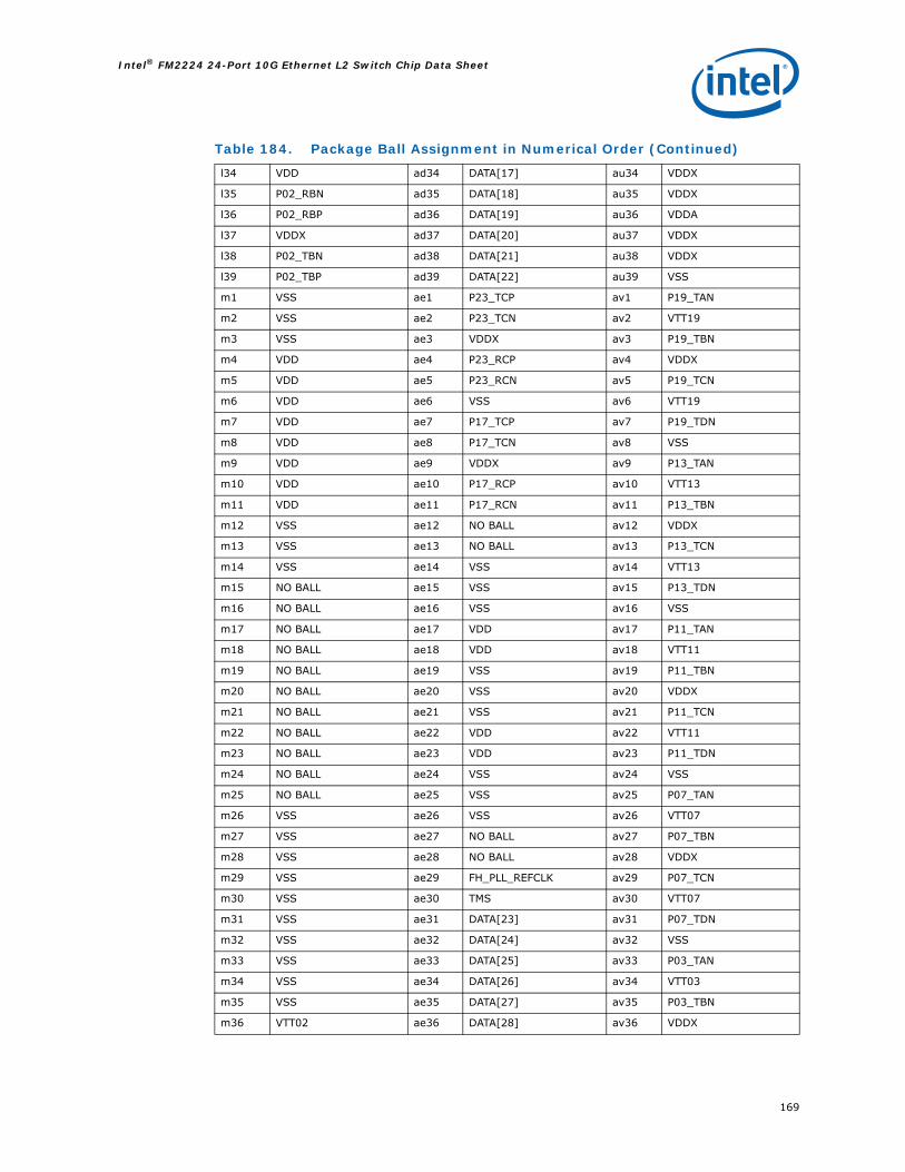
169
Intel® FM2224 24-Port 10G Ethernet L2 Switch Chip Data Sheet
l34 VDD ad34 DATA[17] au34 VDDX
l35 P02_RBN ad35 DATA[18] au35 VDDX
l36 P02_RBP ad36 DATA[19] au36 VDDA
l37 VDDX ad37 DATA[20] au37 VDDX
l38 P02_TBN ad38 DATA[21] au38 VDDX
l39 P02_TBP ad39 DATA[22] au39 VSS
m1 VSS ae1 P23_TCP av1 P19_TAN
m2 VSS ae2 P23_TCN av2 VTT19
m3 VSS ae3 VDDX av3 P19_TBN
m4 VDD ae4 P23_RCP av4 VDDX
m5 VDD ae5 P23_RCN av5 P19_TCN
m6 VDD ae6 VSS av6 VTT19
m7 VDD ae7 P17_TCP av7 P19_TDN
m8 VDD ae8 P17_TCN av8 VSS
m9 VDD ae9 VDDX av9 P13_TAN
m10 VDD ae10 P17_RCP av10 VTT13
m11 VDD ae11 P17_RCN av11 P13_TBN
m12 VSS ae12 NO BALL av12 VDDX
m13 VSS ae13 NO BALL av13 P13_TCN
m14 VSS ae14 VSS av14 VTT13
m15 NO BALL ae15 VSS av15 P13_TDN
m16 NO BALL ae16 VSS av16 VSS
m17 NO BALL ae17 VDD av17 P11_TAN
m18 NO BALL ae18 VDD av18 VTT11
m19 NO BALL ae19 VSS av19 P11_TBN
m20 NO BALL ae20 VSS av20 VDDX
m21 NO BALL ae21 VSS av21 P11_TCN
m22 NO BALL ae22 VDD av22 VTT11
m23 NO BALL ae23 VDD av23 P11_TDN
m24 NO BALL ae24 VSS av24 VSS
m25 NO BALL ae25 VSS av25 P07_TAN
m26 VSS ae26 VSS av26 VTT07
m27 VSS ae27 NO BALL av27 P07_TBN
m28 VSS ae28 NO BALL av28 VDDX
m29 VSS ae29 FH_PLL_REFCLK av29 P07_TCN
m30 VSS ae30 TMS av30 VTT07
m31 VSS ae31 DATA[23] av31 P07_TDN
m32 VSS ae32 DATA[24] av32 VSS
m33 VSS ae33 DATA[25] av33 P03_TAN
m34 VSS ae34 DATA[26] av34 VTT03
m35 VSS ae35 DATA[27] av35 P03_TBN
m36 VTT02 ae36 DATA[28] av36 VDDX
Table 184. Package Ball Assignment in Numerical Order (Continued)

Intel® FM2224 24-Port 10G Ethernet L2 Switch Chip Data Sheet
170
m37 VDDX ae37 DATA[29] av37 P03_TCN
m38 VTT02 ae38 DATA[30] av38 VTT03
m39 VSS ae39 DATA[31] av39 P03_TDN
n1 P24_TAP af1 VSS aw1 P19_TAP
n2 P24_TAN af2 VTT23 aw2 VSS
n3 VSS af3 VDDX aw3 P19_TBP
n4 P24_RAP af4 VTT23 aw4 VSS
n5 P24_RAN af5 VSS aw5 P19_TCP
n6 VDD af6 VDD aw6 VSS
n7 P18_TAP af7 VSS aw7 P19_TDP
n8 P18_TAN af8 VTT17 aw8 VSS
n9 VSS af9 VDDX aw9 P13_TAP
n10 P18_RAP af10 VTT17 aw10 VSS
n11 P18_RAN af11 VSS aw11 P13_TBP
n12 VDDX af12 VDDX aw12 VSS
n13 RCK4AP af13 RCK3AP aw13 P13_TCP
n14 RCK4BP af14 RCK3BP aw14 VSS
n15 NO BALL af15 VSS aw15 P13_TDP
n16 NO BALL af16 VSS aw16 VSS
n17 NO BALL af17 VDD aw17 P11_TAP
n18 NO BALL af18 VDD aw18 VSS
n19 NO BALL af19 VSS aw19 P11_TBP
n20 NO BALL af20 VSS aw20 VSS
n21 NO BALL af21 VSS aw21 P11_TCP
n22 NO BALL af22 VDD aw22 VSS
n23 NO BALL af23 VDD aw23 P11_TDP
n24 NO BALL af24 VSS aw24 VSS
n25 NO BALL af25 VSS aw25 P07_TAP
n26 RCK2BP af26 RCK1BP aw26 VSS
n27 RCK2AP af27 RCK1AP aw27 P07_TBP
n28 VDDX af28 VDDX aw28 VSS
n29 VSS af29 NC aw29 P07_TCP
n30 NC af30 TDO aw30 VSS
n31 CONT_EN af31 NC aw31 P07_TDP
n32 VSS af32 NC aw32 VSS
n33 CHIP_RESET_N af33 NC aw33 P03_TAP
n34 VSS af34 VSS aw34 VSS
n35 P02_RAN af35 VSS aw35 P03_TBP
n36 P02_RAP af36 VSS aw36 VSS
n37 VSS af37 VSS aw37 P03_TCP
n38 P02_TAN af38 VSS aw38 VSS
n39 P02_TAP af39 VSS aw39 P03_TDP
Table 184. Package Ball Assignment in Numerical Order (Continued)

171
Intel® FM2224 24-Port 10G Ethernet L2 Switch Chip Data Sheet
6.5 Package Dimensions
Figure 34. FM2224 Package Bottom View

Intel® FM2224 24-Port 10G Ethernet L2 Switch Chip Data Sheet
172
Figure 35. FM2224 Package Top View (relative to the bottom view, the package has been flipped holding the a1-aw39 diagonal constant)
Figure 36. FM2224 Package Side View
Figure 37. Expanded Detail B of Side View
Table 185. Dimensions Used in Figures
Dimensional References
Reference Min Nom Max
A 2.67 3.07 3.47

173
Intel® FM2224 24-Port 10G Ethernet L2 Switch Chip Data Sheet
Notes: 1. All dimensions are in millimeters.
2. “e” represents the basic solder ball grid pitch.
3. “M” represents the basic solder ball matrix size, and symbol “N” is the maximum allowable number of balls after depopulating.
4. Primary datum C and Seating Plane are defined by the spherical crowns of the solder balls.
5. Package surface is Ni plated.
6. Black spot (or circular etch) for pin 1 identification.
7. Dimensioning and tolerancing per ASME Y14.5M 1994
6.6 Power Dissipation and Heat Sinking
6.6.1 Power Dissipation
The power dissipation of the FM2224 is dependent on a number of different operational factors including:
• The number of ports in operation• The operating rate of each port (10 Gbps, 2.5 Gbps, 1.0 Gbps, etc)• The utilization factor of each port (the percentage of the bit stream that is actual
data, vs. 8B/10B idle characters)• The distribution of frame sizes• SerDes drive strengths• Use of the CPU interface• Supply voltages• Temperature
Though the dependencies above have a considerable effect on supply current draws and overall power dissipation, useful guidelines can be provided through measured data under two operating conditions. One condition consists of the most aggressive possible values for the parameters that have the most impact, namely utilization percentage
A1 0.39 0.49 0.59
A2 2.18 2.58 2.98
D 39.80 40.00 40.20
D1 38.0 BSC
E 39.80 40.00 40.20
E1 38.0 BSC
e 1.00 BSC
M 39
N 1433
Ref.: JEDEC MS-034 B
Table 185. Dimensions Used in Figures (Continued)

Intel® FM2224 24-Port 10G Ethernet L2 Switch Chip Data Sheet
174
and frame size. Other parameters such as SerDes drive strength, supply voltages and case temperatures are kept at nominal values. A second, more typical use model assumes more moderate values for frame sizes and utilization percentages, while keeping the other parameters at their nominal values. The test conditions and resulting current draws and overall power dissipation values are shown in Table 186 and Table 187.
Notes: (1) IDDA is approximately 10 mA per port and is measured as a part of IDDX.
(2) VDDA33 is approximately 4 mA.
(3) VDD33 is used for the CPU interface and no current is drawn when not in use.
(4) Using VDDX = 1.2V will raise power dissipations by up to 4W, depending on use parameters.
(5) Using VDD = 1.25V will increase power dissipation by 2.5W under the most aggressive use conditions and by 1.5W under typical use conditions.
6.6.2 Heat Sinking
It is anticipated that a heat sink will be required for most FM2224 applications. Intel® has successfully used two copper heat sinks designed by Intel® and manufactured by Radian Heatsinks of Santa Clara, CA (www.radianheatsinks.com), which when reasonable air flow is present, leads to acceptable case temperatures.
Table 186. Conditions for Power Measurements
Parameter Aggressive Case Typical
Operating ports 24 24
Operating rate, all ports 10 Gbps 10 Gbps
Utilization factor 100% 50%
Frame size 64B 256B
SerDes drive parameters Nominal Nominal
CPU utilization Not in use Not in use
Supply voltages Nominal Nominal
Temperature, case ~60ºC ~60ºC
Frame handler clock 360 MHz 360 MHz
Table 187. FM2224 Currents and Power
Power Supply Currents (A)
IDD IDDX ITTTotal Power (W)
(VDD=1.2V) (VDDX=1.0V) (VTT=1.5V)
Typical Use 12 6.1 2.0 23.5
Most Aggressive 22.6 6.1 2.0 36.2

175
Intel® FM2224 24-Port 10G Ethernet L2 Switch Chip Data Sheet
The two heat sink designs that have been tested have Radian model numbers FUL003 and FUL004/5. The FUL003 design occupies a smaller area of approximately 64mm x 64mm and is taller at just over 25mm in height. The FUL004/5 design occupies a larger footprint of 80mm x 100mm but is only 8.5mm in height. The thermal characteristics (θCA) of the two heat sink designs are approximately equal.
The overarching goal of heat sink design is to keep the operating case temperature of the device below its maximum allowed value. This will also ensure that the junction stays below its maximum allowable temperature of 125 ºC. With a junction-to-case thermal resistance (θJC) of only 0.15 ºC/W, even the highest allowed value of case temperature, 115ºC, will keep the junction temperature below 125ºC. This is true even assuming a worst case power dissipation approaching 40W, which results in a 6ºC rise in junction temperature over case temperature (40W x 0.15ºC/W = 6ºC).
An effective thermal design solution requires knowledge of several parameters of the device package and heat sink, and of the expected ambient temperature and air flow over the device. The relevant package and heat sink parameters are listed in Table 188.
Notes: (1) This parameter is similar to JB as defined by JEDEC, except that the presence of an isothermal cold ring is not assumed. The value of JB is more relevant to real world use scenarios.
(2) The PC board is assumed to be at ambient temperature.
The parameters above are illustrated in Figure 38. With a knowledge of these parameters and the ambient air temperature surrounding the device, the degree of airflow required to keep the case temperature below the specified maximum can be determined.
Table 188. Thermal Parameters
Parameter Description Value
θJC Thermal resistance, junction to case 0.15 ºC/Watt
ΨJB1,2 Thermal resistance, junction to board 3.5 ºC/Watt
θCA Thermal resistance, case to ambient with heat sink in place.
100 LFM 1.2 ºC/Watt (typ)
150 LFM 0.9 ºC/Watt (typ)
200 LFM 0.75 ºC/Watt (typ)
TCASE(max) Maximum case temperature
Commercial, -C 85 ºC
Extended, -E 105 ºC
Industrial, -I 115 ºC

Intel® FM2224 24-Port 10G Ethernet L2 Switch Chip Data Sheet
176
Figure 38. Thermal Pathways and Corresponding Thermal Resistances
Alternatively, if the airflow is known, the maximum ambient temperature can be calculated.
As an example, if the known parameters are:• FM2224-F1433-C, 85ºC max case temperature• 36W maximum power dissipation• Airflow = 150 LFM
Then the overall temperature rise from case to ambient can be calculated as:
With the values of θCA and θJB from Table 188, this equates to a temperature rise of 26ºC. With a maximum case temperature of 85ºC , a maximum ambient temperature of 59ºC is allowed. If higher ambient temperatures are desired, an increase in airflow or the use of the Extended temperature range (-E) device may be required.
6.6.3 Temperature Sensor Operation
The FM2224 has an integrated temperature sensing diode on board with LVTTL outputs DIODE_IN and DIODE_OUT. Die temperature is read using these outputs through a temperature sensor IC such as the National LM95231. The temperature as reported by this IC has been checked in temperature controlled conditions across a range of temperatures. It was found that the LM95231 measured temperature was higher than the controlled case temperature by approximately 11 to 13 °C. Table 189 shows the corrections that must be applied to the LM95231 temperature to arrive at the correct case temperature. Temperature readings with this IC are not expected to be degree-

177
Intel® FM2224 24-Port 10G Ethernet L2 Switch Chip Data Sheet
accurate, but approximately +/- 5°C. Temperature accuracy with other IC's is unspecified and may vary significantly from the table below, especially for those IC's where series resistance nulling is used.
Table 189. LM95231 Temperature Offsets
Tcase Tmeas (LM95231) Tmeas - Tcase
-44.6 -33.0 11.6
-27.4 -15.0 12.4
-10.0 2.5 12.5
7.6 20.0 12.4
31.4 44 12.6
35.8 48.5 12.7
50.0 62.5 12.5
70.0 82.5 12.5
92.4 105.0 12.6
110.8 123.5 12.7
119.4 132.5 13.1
120.5 133.5 13.0

Intel® FM2224 24-Port 10G Ethernet L2 Switch Chip Data Sheet
178
7.0 Document Revision Information
The following table lists the changes made to the FM2224 Datasheet resulting in the publication of a new revision.
7.1 Nomenclature
Document revisions are placed in either of two categories to allow the user to quickly focus on changes of a substantive nature (Category 1), that is, changes that may have an impact on system or board level design.
Category 1 changes are specification clarifications or changes and include modifications to the current published specifications, or describe a specification in greater detail or further highlight a specification's impact to a complex design situation. These clarifications and changes will be incorporated in any new release of the specification or other affected document.
Category 2 changes are documentation changes and include corrections for typos, errors, or omissions from the current published specifications. These will be incorporated in any new release of the specification.
7.2 Rev 1.0 to 1.1 changes
PageCategory
Description1 2
1 54 X Removed references to a switch priority protected from the PWD mechanism. Also noted in QUEUE_CFG_1 register.
2 122 X Added note of clarification to Table 108
3 83 X Figure 31: Removed reference to DS_N pin, which does not exist.
4 19 X Table 41: Changed Fat Tree image.
5 94 X Added version number for A5 silicon.
6 170 X Corrected dimension A in Table 184. Min and Max were reversed.
7 78 X Updated Figure 30, provisioning vs. Vdd and Tcase. 0.1V higher Vdd is needed to guarantee provisioning level.
8 88 X Table 32: Added statistics and counter register tables to register map
9 32 X Table 1: Corrected RCK to port assignments for the 4 port groups.
10 151 X Table 174: Corrected RCK to port assignments for the 4 port groups.
11 136 X Table 139: Recommend setting “Ignore IFG errors” and “Ignore preamble” errors bits.
12 136 X Table 139: Change bits 3:0 from reserved to LF, controlling the /K/A/R randomization.
13 157 X Added note on power supply sequencing
14 155 X Table 180: Changed TESTMODE pin from “leave unconnected” to “pull down”.

179
Intel® FM2224 24-Port 10G Ethernet L2 Switch Chip Data Sheet
7.3 Rev 2.0 to 2.1 changes
7.4 Rev 2.1 to 2.2 changes
15 81 X Table 23: Add note on overshoot for VIH on LVTTL inputs.
16 119 X Table 100: QUEUE_CFG_1, TX shared watermark. Remove text to the effect that switch priority 15 is exempt from PWD dropping
17 114 X Table 90: Include new definitions of 3 bits in TRUNK_HASH_MASK table.
18 121 X Table 104: Documented QUEUE_CFG_5 register, which had been missing.
19 134 X Table 134: BIST mode 0x2 corrected to D21.5 pattern.
20 - X Removed references to FUSEBOX and SHADOW FUSEBOX register operations in several locations. Fusebox processing is not customer configurable.
21 67 X Added serdes power-up procedure to Step 4 of Bring-up without EEPROM procedure.
PageCategory
Description1 2
1 170 X Corrected min and max “A” dimensions.
2 174 X Made several additions/corrections to the page numbers and Table numbers in Rev 1.0 to 2.0 change table.
3 156 X Table 181: removed pin af30 from list of no-connect pins. It is TDO.
4 157 X Clarified power sequencing at boot-up.
5 129 X Table 121, VLANEgressBVDrops: removed the word “unicast” as this applies to multicast also
7 94 X Table 42, Bypass bit: Replace CPU_CLK with FH_PLL_REFCLK, as this is the actual PLL reference clock.
8 72 X Added section 3.5.5.1, clarifying the LED clock divider scheme
9 93 X Table 39: clarified LEDfreq description.
10 75 X Table 17: Update silicon version bit description.
11 130 X Table 122: changed offset for TXMulticast register to 0x70024+0x200*i
PageCategory
Description1 2
1 173 X Added section 6.6.3 on Temperature Sensor Operation
2 72 X Added Table 14: SPI write sequence.
3 43 X Improve description of Discard Egress Boundary Violation
4 106 X Clarify behavior of PORT_CFG_1:VLAN ingress port precendence
5 105 X PORT_CFG_1[1..24] and PORT_CFG_2[1..24] are defined for Port 0, so changed to PORT_CFG_1[0..24] and PORT_CFG_2[0..24]
6 126 X Added text explaining that counters may not be able to keep up with worst case traffic on all ports.
7 78 X Recommended Operating Conditions, Note 4: added note of caution if using Vddx = 1.2V.

Intel® FM2224 24-Port 10G Ethernet L2 Switch Chip Data Sheet
180
7.5 Rev 2.2 to 2.3 changes
§ §
8 114 X Table 91 TRUNK_HASH_MASK: Modify VLAN-PRI to note that the CFI bit is included.
9 44 X Removed reference to support for IGMPv3 Snooping. Limitations on its use render it not practical to use.
10 119 X Table 101: Bit names changed to Tx and Rx Hog watermarks. They are not associated with PWD.
11 69 X Section 3.5.4: Change Wait command description to express wait cycles in terms of SPI clock, not CPU clock.
12 86 X Table 29: Corrected register addresses for PORT_VLAN_IP1/2 and PORT_VLAN_IM1/2.
13 93 X Table 41: Frame Timer default changed to 0x0
14 141 X Table 153: Inclued recommendations for setting value of PAUSE resend interval
15 130 X Group 7 Counters: Modify Unicast, Multicast and Broadcast to include possible bad FCS frames.
PageCategory
Description1 2
1 71 X Removed reference to SGS M5450 LED driver
2 84 X Added notes to CPU timing spec.
3 94 X Added to the description of FRAME_TIME_OUT