integration of dye lasers and microfluidics for biochemical analysis
TRANSCRIPT

Integration of Dye Lasers and Microfluidics for Biochemical Analysis
Thesis by
Yan Chen
In Partial Fulfillment of the Requirements
for the Degree of
Doctor of Philosophy
California Institute of Technology
Pasadena, California
2009
(Defended July 18th, 2008)

ii
2009
Yan Chen
All Rights Reserved

iii
Acknowledgements
The six years at Caltech have been the most memorable time in my life so far, I owe
many thanks for my experience here. First of all, I would like to thank my advisor, Prof.
Axel Scherer, for providing me with the opportunity and resources to complete my Ph.D. at
Caltech. I am grateful to his guidance and support through all these years. His broad
perspective, valuable advice, and sincere mentorship have always been a source of
inspiration and motivation.
I would also like to thank my committee members: Prof. Changhuei Yang, Prof. Oskar
Painter, Prof. Yu-Chong Tai, and Prof. Chin-Lin Guo, and other members in my candidacy
committee: Prof. Mory Gharib, and Prof. Mladen Barbic.
My great thanks go to my collaborators: Dr. Zhenyu Li and Dr. John Zhong. It has
been great to work with Dr. Zhenyu Li, I am most grateful for all the helpful discussions
and valuable advice from him. Collaboration with Dr. John Zhong in USC Medical School
has been very fruitful and enjoyable. I thank him for providing many valuable resources for
research, and being a great friend.
The Nanofabrication group is a great place to work and study. I would like to thank all
the members in the Caltech Nanofabrication Group. I would first like to thank Dr. Zhaoyu
Zhang, who helped me get started from the first day I arrived in the lab. I also benefit a lot
from many of our former group members, Dr. George Maltezos, Dr. Saurabh Vyawahare,
Dr. Tereal Neal, Dr. Koichi Okamoto, Dr. Michael Hochberg, Dr. Tom Baehr-Jones, Dr.
Emil Kartalov, and Dr. Joyce Wong. I am grateful to the remaining members of the
Nanofabrication group for their support and help in the lab, and their friendship, Chris

ivWalker, Teresa Emery, Lin Zhu, David Henry, Michael Shearn, Uday Khankhoje,
Guangxi Wang, Ting Hong, Jingqing Huang, and Sameer Walavalkar. I would like to thank
our secretary, Kate Finigan, and our lab coordinator, Dr. Guy DeRose, who have been
working hard to enable an efficient working environment for all of us. I have been
extremely fortunate to work with so many wonderful people in my time at Caltech.
Finally, but most importantly, I am eternally grateful to my parents and my
grandmother for their unconditional love, constant support and confidence in me
throughout my life. Above all I owe my deepest thanks to Jiarui Han, for his tremendous
love, encouragement, and support during the past six years, none of this could have been
accomplished without him.

v
Abstract
This dissertation describes the study of two important aspects of integration in
microfluidics: optics and biochemistry. In optics integration, two types of miniaturized dye
lasers, namely the solid-state polymer dye lasers and optofluidic dye lasers were
demonstrated. Both of the dye lasers possess a resonant cavity with circular grating
geometry, and they are suitable to serve as low-threshold, surface-emitting coherent light
source in microfluidic networks. The mass production and large scale fabrication of such
low-cost dye laser arrays can be realized by the well developed nanoimprint and soft
lithography, making this technology attractive for various biochemical applications. In
biochemistry integration, a microfluidic system was developed to fully utilize the
complexity of microfluidic circuits to process single cells and extract gene expression
information in a parallel manner. The work presented here explored both the optics and
biochemistry integration in microfluidics, which are the key issues for further development
of complete “lab-on-a-chip” systems.

vi

vii
Contents
Acknowledgements .............................................................................................................iii
Abstract ................................................................................................................................. v
List of Figures ....................................................................................................................... x
List of Tables ...................................................................................................................... xv
Glossary of Acronyms ...................................................................................................... xvi
1 Introduction .................................................................................................................. 1
1.1 Overview ............................................................................................................... 1
1.1.1 Optics in microfluidics ............................................................................. 1
1.1.2 Biochemistry in microfluidics ................................................................. 3
1.2 Thesis organization ............................................................................................... 4
2 Modeling of Circular Grating Structure by Transfer Matrix Method ................. 5
2.1 Introduction ........................................................................................................... 5
2.1.1 Circular gratings ....................................................................................... 5
2.1.2 Transfer matrix method ............................................................................ 7
2.2 Transfer matrix analysis ....................................................................................... 8
2.2.1 Maxwell’s equation .................................................................................. 8
2.2.2 Transfer matrix method .......................................................................... 11
2.2.3 Transfer matrix method coefficients ...................................................... 14
2.3 Simulation results ............................................................................................... 17
2.3.1 Index matching ....................................................................................... 17
2.3.2 Cavity resonance .................................................................................... 19

viii2.3.3 Electromagnetic field plot ...................................................................... 23
3 Nanoimprinted Circular Grating Dye Laser .......................................................... 25
3.1 Introduction ......................................................................................................... 25
3.2 Materials ............................................................................................................. 28
3.2.1 PMMA .................................................................................................... 28
3.2.2 Organic dye ............................................................................................ 28
3.2.3 Cytop ...................................................................................................... 29
3.3 Laser cavity design ............................................................................................. 30
3.4 Fabrication process ............................................................................................. 31
3.4.1 Imprint mold fabrication ........................................................................ 31
3.4.2 Laser chip fabrication ............................................................................. 34
3.4.3 Nanoimprint process .............................................................................. 35
3.5 Results and discussion ........................................................................................ 38
3.6 Summary ............................................................................................................. 42
4 Optofluidic Circular Grating Dye Laser ................................................................. 43
4.1 Introduction ......................................................................................................... 43
4.2 Materials ............................................................................................................. 46
4.2.1 PDMS ..................................................................................................... 46
4.2.2 PFPE ....................................................................................................... 47
4.2.3 Laser dye and solvents ........................................................................... 49
4.3 Laser cavity design ............................................................................................. 51
4.3.1 Circular grating distributed feedback structure ..................................... 51
4.3.2 Flow channel design ............................................................................... 53
4.4 Fabrication process ............................................................................................. 55
4.4.1 Mold fabrication ..................................................................................... 55
4.4.2 Laser chip fabrication ............................................................................. 59
4.5 Results and discussion ........................................................................................ 62
4.6 Summary ............................................................................................................. 65

ix
5 Microfluidic Device as a Platform for Single Cell
Biochemical Analysis ................................................................................................. 66
5.1 Introduction ......................................................................................................... 66
5.1.1 Microfluidic device as a platform for biochemical analysis ................. 66
5.1.2 Significance of single-cell gene analysis ............................................... 67
5.2 Design of microfluidic devices for single-cell analysis .................................... 69
5.2.1 First generation of microfluidic chip ..................................................... 69
5.2.2 Second generation of microfluidic chip ................................................. 70
5.3 Materials and methods ........................................................................................ 72
5.3.1 Mold fabrication ..................................................................................... 72
5.3.2 Device fabrication .................................................................................. 72
5.3.3 Microfluidic station ................................................................................ 73
5.3.4 Synthesis of cDNA from hESCs............................................................ 74
5.4 Operation of microfluidic device ....................................................................... 75
5.5 Results and discussion ........................................................................................ 77
5.5.1 Device efficiency .................................................................................... 77
5.5.2 Gene expression of single hESC cells ................................................... 80
5.6 Conclusions ......................................................................................................... 82
6 Summary ..................................................................................................................... 85
Appendix A ......................................................................................................................... 87
Appendix B ......................................................................................................................... 90
Bibliography ....................................................................................................................... 93

x
List of Figures
2.1 Diagram of a circular grating resonator design. The scheme illustrates the
second-order Bragg diffraction including (1) normal diffraction to the grating surface
(first-order) and (2) in-plane feedback (second-order) ......................................................... 6
2.2 Schematic representation of a circular grating, with grating period , duty cycle
/wdc , effective indices In and IIn , cavity radius 121 ,,, Nrrr .......................... 11
2.3 Effective index approximation of solid-state dye laser ............................................ 28
2.4 Effective index approximation of optofluidic dye laser ........................................... 17
2.5 The power ratio in circular grating with period of 440 nm for m=0,1,2 .................. 19
2.6 The power ratio in circular grating with period varying from 400 nm to 450 nm ... 20
2.7 The power ratio in circular grating with two groove depths .................................... 21
2.8 The power ratio in circular grating with period varying from 400 nm to 440 nm ... 22
2.9 The 1-D graph of the normalized mjzH , field in circular grating for m=0,1 .......... 23
2.10 The 3-D graph of the normalized mjzH , field in circular grating for m=0,1 .......... 23

xi
3.1 The general nanoimprint process............................................................................... 26
3.2 Schematic diagram of a nanoimprinted circular grating dye laser chip ................... 27
3.3 The monomer building block of PMMA .................................................................. 28
3.4 Rhodamine 640 molecule structure ........................................................................... 29
3.5 Cytop molecule structure ........................................................................................... 29
3.6 General design of a circular grating distributed feedback structure ......................... 30
3.7 The SEM image of the cross section of an etched SiO2 grating ............................... 31
3.8 Schematic fabrication procedure for the circular grating nanoimprint hard mold. (a)
The original wafer with 500 nm SiO2 on top of silicon substrate. (b) PMMA is spun on the
sample for subsequent e-beam lithography steps. (c) The PMMA is exposed by b-beam,
and the circular grating pattern is completely transferred into PMMA after developing the
exposed resist. (d) The pattern is transferred into the SiO2 via CHF3 RIE etch, and the
PMMA residue is removed after dry etch ........................................................................... 32
3.9 SEM images of (a) the top view and (b) the angled view of SiO2 mold .................. 33
3.10 Summary of the Cytop and PMMA substrate preparation process .......................... 35
3.11 Schematic nanoimprint process of circular grating polymer dye laser .................... 36
3.12 SEM images of (a) the SiO2 mold and (b) the imprinted PMMA film .................... 37

xii3.13 Measurement setup for polymer dye laser device ..................................................... 38
3.14 Nanoimprinted circular grating DFB dye laser spectrum. The measured linewidth is
0.18 nm. Inset: Polymer laser chip excited by Nd:YAG 532nm laser pulse ..................... 39
3.15 The output laser power vs. the absorbed pump energy curve. The threshold pump
fluence is 1.31 μJ/mm2 ........................................................................................................ 40
3.16 (a) Far-field image of the emission pattern recorded by a CCD camera. (b) Circular
grating DFB laser far-field radiation patterns through a linear polarizer with different
orientation angles ................................................................................................................. 41
4.1 Schematic diagram of an optofluidic circular grating dye laser chip ....................... 45
4.2 Rhodamine 6G molecule structure ............................................................................ 49
4.3 Cross sections of stimulated singlet state absorption and emission for Rhodamine 6G
in ethanol .................................................................................................................... 49
4.4 General design of an optofluidic circular grating DFB dye laser cavity .................. 51
4.5 Illustration of the Bragg diffraction in the second-order circular grating. First-order
Bragg reflection induces coupling to vertical propagating waves, and second-order
Bragg reflection leads to in-plane feedback .............................................................. 52
4.6 PDMS microvalves (push-down version). Source: www.fluidigm.com ................. 53
4.7 Microscope graph of microfluidic flow channel. Left: flow channel covering the
grating area. Right: flow channel filled with dye solution ....................................... 54

xiii4.8 Schematic fabrication procedure for the circular grating hard mold. (a) The
original wafer with 1 µm SiO2 on top of silicon substrate. (b) Cr is evaporated on the
sample. (c) PMMA is spun on top of the Cr for subsequent e-beam lithography steps.
(d) The PMMA is exposed by e-beam, and the circular grating pattern is completely
transferred into PMMA after developing the exposed resist. (e) The Cr underneath
the exposed pattern is removed by wet etch, and the remaining PMMA is also
removed. (f) The pattern is transferred into the SiO2 via DRIE etch ....................... 56
4.9 The SEM images of the cross-section of etched SiO2 gratings. (a) A cut-away view of
the gratings. (b) Deeply etched trenches in the circular grating structure ................ 57
4.10 SEM images of (a) the top view and (b) the angled view of the SiO2 mold ............ 58
4.11 Fabrication process of hybrid PFPE/PDMS laser chip ............................................. 60
4.12 (a) SEM images of SiO2 mold. (b) ESEM images of PFPE replica ......................... 61
4.13 Measurement setup of optofluidic dye laser chip ..................................................... 62
4.14 Optofluidic circular grating DFB dye laser spectrum. Inset: The output laser power
vs. the pump energy curve ......................................................................................... 63
5.1 20X single-cell mRNA extraction microfluidic device filled with food dye ........... 69
5.2 32X single-cell gene profiling microfluidic device filled with food dye ................. 71
5.3 The setup of the microfluidic device for single hESC mRNA extraction. (a) The
system includes a microscope, a computer to control air pressure with pressure
regulators, and a heating plate. (b) A typical microfluidic chip ............................... 73

xiv5.4 Merged image of immunofluorescent-stained (Oct-3/4) and light microscope
images from a pluripotent hESC colony ................................................................... 74
5.5 The process flow in the single-cell microfluidic processor ...................................... 76
5.6 Measuring absolute molecule numbers of three genes in single hESC with multiplex
quantitative PCR ........................................................................................................ 79
5.7 Expression of B2M, Nodal, and Fzd4 in single hESC ............................................. 81

xv
List of Tables
4.1 Refractive indices of PDMS-compatible solvents .................................................... 50
5.1 Microfluidic device increasing mRNA capture and reverse transcription (RT)
efficiency .................................................................................................................... 78

xvi
Glossary of acronyms
2D – Two-dimensional
DBR – Distributed Bragg reflector
DFB – Distributed feedback
ESEM – Environmental scanning electron microscope
FDTD – Finite difference time domain
FP – Fabry-Perot
FWHM – Full width at half maximum
MIBK – Methyl isobutyl ketone
OSA – Optical spectrum analyzer
PL – Photoluminescence
RIE – Reactive ion etching
PMMA – Poly(methyl methacrylate)
Q – Quality factor
SEM – Scanning electron microscope

1
Chapter 1
Introduction
1.1 Overview
1.1.1 Optics in microfluidics
The field of microfluidics continues to become an important area with novel applications in
biotechnology [1]. The most important goal for microfluidics is to achieve a complete
“lab-on-a-chip” system, which is capable of performing biological and chemical
experiments normally carried out in a standard full-size laboratory. While efforts are made
to develop the microfluidic system to realize more functionality for various biochemical
reactions, the integration of optical components into microfluidic systems becomes more
and more indispensable.
Optical detection and spectroscopic analysis are important in most micrototal analysis
systems (μTAS) [2]. Currently a majority of microfluidic systems are based on external
light sources. However, the coupling of optical signals in and out of the devices, typically
by optical fibers, remains one of the major challenges in integrated optics. By making
on-chip light sources, we can eliminate the optics alignment, which greatly reduces the
complexity of the system. Therefore, the integration of miniaturized active light sources
such as lasers into microfluidic systems becomes an attractive approach for biological and
chemical processes.

2We are very interested in the miniaturization and integration of dye lasers into
microfluidic systems because of their broadband tunablity, low cost, and easy fabrication.
Dye lasers have been widely used as tunable, coherent light sources for spectroscopic
analysis in the visible wavelength region (from 400 nm to 900 nm) during the past 30 years
[3]. Miniaturized dye lasers, which can be integrated in lab-on-a-chip microsystems, would
similarly have numerous applications. For applications in biochemical analysis in
microfluidic systems, a surface emitting laser is more useful than other lasers because of its
stacked substrate structure. Therefore, we choose a circular grating structure as the laser
resonator design to produce low-threshold surface emitting lasing. The laser operating
characteristics can be significantly improved by the two-dimensional nature of the
resonator structure.
Two types of miniaturized dye lasers with the circular grating geometry are
demonstrated in this thesis: solid-state and optofluidic dye lasers. For the solid-state dye
laser, the laser dye is doped in the polymer forming the laser resonator, and it is fabricated
using nanoimprint lithography. For the microfluidic dye laser, the laser dye is dissolved in
an organic solvent and flowed through a microfluidic channel with laser resonator
embedded, and it is realized by soft lithography. They can produce high-intensity and
narrow-linewidth lasing with a well-defined output beam.
The well developed nanoimprint and microfluidics technology provide a convenient
way of mass production and large-scale fabrication of low-cost dye laser arrays with a wide
wavelength output range. It is also straightforward to build on-chip dye lasers with
waveguides to replace the optical fibers necessary for the integrated optics. The
miniaturized dye lasers can serve as surface emitting coherent light sources, which are very
important in various biochemical applications, such as laser-induced fluorescence and
spectroscopy.

31.1.2 Biochemistry in microfluidics
As we study the optical integration in microfluidic systems towards fully functional
“lab-on-a-chip” system, we are exploring more capabilities of the microfluidic system in
the field of biochemical analysis. Lab-on-a-chip devices have the potential to revolutionize
biochemistry by allowing complicated biochemical procedures to be performed on a small
microfluidic chip. Single-cell processing is one of the major applications of microfluidics
that can take advantage of its nanoliter fluid handing abilities.
A microfluidic approach that can extract gene expression information from individual
single cells is described in this thesis. The integrated process: cell capture/lysis, mRNA
isolation/purification, and cDNA synthesis/purification for single human embryonic stem
cells is implemented on a microfluidic device. With the improved design of the
microfluidic circuit, a parallel processing of dozens of cells with 100% efficiency can be
achieved.
The gene expression of human embryonic stem cells (hESC) is a critical aspect for
understanding the normal and pathological development of human cells and tissues.
Current bulk gene expression assays rely on RNA extracted from cell and tissue samples
with various degree of cellular heterogeneity. These “cell population averaging” data are
difficult to interpret, especially for the purpose of understanding the regulatory relationship
of genes in the earliest phases of development and differentiation of individual cells. Here,
we report a microfluidic approach that can extract total mRNA from individual single cells
and synthesize cDNA on the same device with high mRNA-to-cDNA efficiency. This
feature makes large-scale single-cell gene expression profiling possible. Using this
microfluidic device, we measured the absolute numbers of mRNA molecules of three genes
in a single hESC. Our results indicate that gene expression data measured from the cDNA
of a cell population is not a good representation of the expression levels in individual single
cells. Within the G0/G1 phase pluripotent hESC population some individual cells did not
express all of the 3 interrogated genes in detectable levels. Consequently, the relative
expression levels, which are broadly used in gene expression studies, are very different

4between measurements from population cDNA and single-cell cDNA. The results
underscore the importance of discrete single-cell analysis, and the advantages of a
microfluidic approach in stem-cell gene expression studies.
1.2 Thesis organization
The thesis is organized as follows: Chapter 2, Chapter 3 and Chapter 4 focus on the optics
integration of the microfluidic system, and Chapter 5 highlights the biochemistry aspect of
the microfluidic system.
Chapter 2 extensively studies the modeling of circular grating resonators using
transfer matrix method. An analytical model is developed to locate the resonance in a
circular grating resonator. Both the parameters from solid-state and optofluidic dye lasers
have been applied to the analytical model, and the simulation results are compared with
experimental data. Chapter 3 describes the fabrication of solid-state polymer dye lasers
using nanoimprint lithography. The detection result of the surface emitting dye laser with a
circular grating geometry is discussed. Chapter 4 presents the fabrication of optofluidic dye
lasers using soft lithography. A hybrid material system is introduced to make functional
microfluidic laser devices. Chapter 5 demonstrates the use of microfluidic system as a
platform to perform single-cell gene analysis. Chapter 6 concludes the thesis with an
outlook of the future work for integration of optics with microfluidics for various
biochemical applications.

5
Chapter 2
Modeling of circular grating structure by transfer matrix method
2.1 Introduction
2.1.1 Circular grating
Laser (Light Amplification by Stimulated Emission of Radiation) is composed of a gain
medium and a resonant optical cavity [4]. The gain medium amplifies the beam by
stimulated emission, and the resonant cavity provides the feedback necessary for the lasing
operation. For our solid-state and optofluidic dye lasers in Chapter 3 and Chapter 4, we
choose the circular grating resonator as laser cavities for their unique two-dimensional
nature and enhanced lasing performance.
In particular, we use the second-order circular grating distributed feedback (DFB)
structure as the resonant cavity. The distributed feedback scheme indicates that the gain
material is directly implemented in the grating structure. The circular grating DFB structure
satisfies the second-order Bragg condition, effBragg n , where Bragg is the emission
wavelength, effn is the effective index of the waveguide mode, and is the grating
period, with an inner cavity providing a quarter- or half-wavelength shift similar to the
classical DFB case.

6
Figure 2.1: Diagram of a circular grating resonator design. The scheme illustrates the
second-order Bragg diffraction including (1) normal diffraction to the grating surface
(first-order) and (2) in-plane feedback (second-order).
The second-order grating is used to obtain surface emission, because it not only
couples counter-propagating radial waves (via second-order Bragg reflection), but also
induces coupling of radially propagating waves into the direction normal to the grating
surface (via first-order Bragg reflection). Fig. 2.1 shows a cut-away diagram of a typical
circular grating resonator. The corrugations in the grating structure provide both distributed
feedback and output coupling of the guided optical mode via second-order and first-order
Bragg scattering.
72.1.2 Transfer matrix method
To understand the resonant behavior of the circular grating, a theoretical analysis is
necessary. There are many methods for modeling circular optical resonators. Most of the
models are based on couple mode theory [5-9], which is more suitable for analyzing
circular grating structure with shallow trenches and a modest light confinement. In this
chapter, we present a transfer matrix method for analyzing circular grating structure with
deep etched trenches. The deeper trenches of the structure lead to stronger in-plane
effective index modulation, therefore the resonator can confine light in a smaller volume.
The transfer matrix method [10] is a straightforward method for analyzing optical
structures composed of an arbitrary number of dielectric layers. When the dielectric
properties are taken into account and the boundary conditions are satisfied, a transfer
matrix can relate the electromagnetic field on either side of an optical region. Therefore, a
complex structure can be modeled by simple matrix multiplication of basic subcomponents.
The transfer matrix method is suitable to analysis of various resonant optical cavities, such
as multi-section Fabry-Perot, DBR, DFB, and VCSEL geometries [11]. For our application,
we are interested in utilizing transfer matrix method for the analysis of structures with
cylindrical symmetry.
In this chapter, we derive a transfer matrix method appropriate for description of the
optical modes of circular grating microcavities. The electromagnetic modes of cylindrical
multilayer structures are analyzed in terms of propagating waves, i.e., Hankel functions. In
this chapter, the theoretical analysis follows the calculations of [12] and [13]. Using this
transfer matrix method based 2-D cylindrical model, the spectrum information of the cavity
modes can be obtained to analyze the energy confinement in the circular grating structure.

8
2.2 Transfer matrix analysis
2.2.1 Maxwell’s equation
To solve the wave equation, we define E
and H
as the vector electric and magnetic
fields in the circular grating structure, and they are represented by ),,( EEE rz and
),,( HHH rz in cylindrical coordinates. In our 2-D model, we simplify the circular Bragg
grating to infinite cylinders, and consider the system invariant in the z direction. Therefore,
the electrical field and magnetic field can be expressed as tierE ),(
and tierH ),(
.
The Maxwell’s equation is given below in its differential form
0
0
H
E
EiH
HiE
(2.1)
where and are the magnetic permeability and dielectric permittivity in the grating
structure, and is the angular frequency of the electromagnetic field.
At all layer interfaces, the tangential components of the electric and magnetic field E
and H
must be continuous. The system is invariant in z direction, therefore the solutions
can be decomposed into two distinct polarizations: transverse electric (TE) and transverse
magnetic (TM). We need to explore the general solutions of the Maxwell’s equations for
the cylindrical symmetry, i.e., Hankel functions, and use them to solve the optical modes
based on the transfer matrix method.

9We can derive the Helmholtz equation from Maxwell’s equation and solve it for the
cylindrical coordinate.
022
H
Ek
(2.2)
where k is the wavenumber in the grating structure and satisfies 22 k .
Expressing the Helmholtz equation in cylindrical coordinates, we have
01
)(1 2
2
2
2
2
2
H
Ek
zrrr
rr
. (2.3)
Because the system is invariant along the z coordinate, the separation in z components and
in a transversal part is possible. Let 222zT kkk , where Tk and zk represent the
component for the polar and z coordinates, respectively.
If we apply the following variable separation to Eq. (2.3),
)()(),(
)()(),(
rRBrH
rRArE
z
z (2.4)
the equation becomes
0)()()()()(1
)()(
)( 22
2
22
2
TkrRr
rR
r
rR
rr
rR . (2.5)
The equation can be separated into two parts with only dependence on r and , and
each part can be solved on its own.
22
222
2
22 )(
)(
1)(
)(
)(
)(mkr
r
rR
rR
r
r
rR
rR
rT
(2.6)

10
The solution of 0)()( 2
2
2
m is either
ime
lmm
lmm
)(
)(),sin()(
),cos()(
21 . (2.7)
The equation below is known as the Bessel differential equation
0)()(
)(
)(
)(222
2
22
mkrr
rR
rR
r
r
rR
rR
rT . (2.8)
Therefore, the general solution of the time harmonic electromagnetic field is the
Hankel function, which is a linear combination of Bessel and the Neumann function,
)()()(
)()()()2(
)1(
riNrJr
riNrJr
mmm
mmm
(2.9)
)1(m and )2(
m are the first-kind and second-kind Hankel functions, respectively, m is
the azimuthal order, mJ is the Bessel function, and mN is the Neumann function.
The solutions of variable separated equations can be inserted into Eq. (2.4),
for the TE mode,
0
)2()1( )]()([),(m
immmmm
jz errrH . (2.10)
for the TM mode,
0
)2()1( )]()([),(m
immmmm
jz errrE . (2.11)

112.2.2 Transfer matrix method
The schematic circular grating laser structure is shown in Fig. 2.2. The circular grating
structure consists of N infinite cylindrical concentric layers. Each layer consists of
alternating dielectric materials with refractive indices In and IIn .
Figure 2.2: Schematic representation of a circular grating structure, with grating period ,
duty cycle /wdc , effective indices In and IIn , cavity radius 121 ,,, Nrrr .

12Our goal is to describe the field propagating in a cylindrical waveguide structure
shown in Fig. 2.2. Due to the 2-D nature of the problem, the field solutions can be
decomposed into TE and TM polarizations, for which the field in the plane is entirely
characterized by ),,( EEH rz and ),,( HHE rz , respectively. The present cylindrical
geometry suggests we expand the fields using first-kind and second-kind Hankel functions,
)1(m and )2(
m , which are linearly independent and represent the inward and outward
propagating circular (Hankel) waves.
We are mainly considering the TE polarization, since the perpendicular pumping light
on the grating surface will cause almost pure excitation of TE waves [23]. As described in
the previous chapter, the general TE solutions of the Maxwell’s equations in each layer j
can be expressed as a linear combination of imjm erkn )( 0
)1( and imjm erkn )( 0
)2( for
each mode ,,1,0 m , jn is the effective refractive index in each layer j .
The H -field is expressed as
0
,
00
)2(0
)1(
)(
)]()([),(
m
immjz
m
imjm
jmjm
jm
jz
erH
erknrknrH
. (2.12)
Based on Maxwell’s equations, EinH j 20 ,
j
jrj
jz
jz
jz
E
Ein
rH
H
H
r
z
0
/
/
0
0
0
/
/
/2
0 (2.13)
0
,
00
)2(0
)1(
20
)(
)]()([1
),(
m
immjr
m
imjm
jmjm
jm
j
jr
erE
merknrknin
rE
(2.14)
13
0
,
00
)2(0
)1(
0
)(
)]()([),(
m
immj
m
imjm
jmjm
jm
j
j
erE
erknrkncn
irE
. (2.15)
)1(m and )2(
m are the derivative of )1(m and )2(
m , respectively.
Similarly, for TM polarization, the E -field is expressed as
0
,
00
)2(0
)1(
)(
)]()([),(
m
immjz
m
imjm
jmjm
jm
jz
erE
erknrknrE
. (2.16)
Based on Maxwell’s equations, HiE 0 ,
j
jr
jz
jz
jz
H
Hi
rE
E
E
r
z
0
/
/
0
0
0
/
/
/
0 (2.17)
0
,
00
)2(0
)1(
0
)(
)]()([1
),(
m
immjr
m
imjm
jmjm
jm
jr
erH
merknrknrH
(2.18)
0
,
00
)2(0
)1(
0
)(
)]()([),(
m
immj
m
imjm
jmjm
jm
jj
erH
erknrknic
nrH
. (2.19)

142.2.3 Transfer matrix method coefficients
At the interface between the thj and thj )1( layers, located at jrr , the tangential
fields components ( HEz , for TM polarization; EH z , for TE polarization) must be
continuous. The coefficients calculations of Transfer Matrix below are based on TE
polarizations.
),(),(
),(),(1
1
jj
zjj
z
jj
zjj
z
rHrH
rErE
(2.20)
The relationship between the coefficients ),( jm
jm , ),( 11 j
mj
m can be expressed by
jm
jm
jm
jm
jm
jm
jm
jm
ab
ba
1
1
(2.21)
where jm
jm ba , are the complex conjugates of j
mj
m ba , .
)()()()(1
)()()()(1
0)2(
01)2(
01)2(
0)2(
0)1(
01)2(
01)2(
0)1(
krnkrnkrnkrnD
b
krnkrnkrnkrnD
a
jjmjjmjjmjjmjm
jm
jjmjjmjjmjjmjm
jm
(2.22)
with the index ratio j
j
n
n 1 ,
)()()()( 01)1(
01)2(
01)2(
01)1( krnkrnkrnkrnD jjmjjmjjmjjm
jm . (2.23)
For TM polarization, the only difference is the index ratio 1
j
j
n
n .

15We can obtain an overall transfer matrix relating the inner cavity to the outmost ring
by multiplying the transfer matrices for each layer. For 1,,2,1 Nj ,
1
1
m
mNmN
m
Nm T
. (2.24)
The overall transfer matrix NmT takes the form
11
11
11
11
mm
mmNm
Nm
Nm
Nm
Nm
Nm
Nm
NmN
mab
ba
ab
ba
AB
BAT (2.25)
with
10
0111
111
mm
mmm
AB
BAT . (2.26)
In order to find resonant modes, we can assume 11mm , since every incoming
wave can be considered as an outgoing one after crossing the z axis. The power in each
layer j can be defined as 22 j
mj
mj
mP .
Therefore the ratio of the electromagnetic power confined in the center ring 1mP to
that in the outmost ring NmP is
22
21211
Nm
Nm
mm
Nm
mm P
PR
(2.27)
111
111
)(
)(
mNm
Nmm
Nmm
Nm
Nm
mNm
Nmm
Nmm
Nm
Nm
BAAB
BABA
(2.28)
with Nm
Nm
Nm
2, N
mNm
Nm
2, we obtain
1622122122 N
mNmm
Nm
Nmm
Nm
Nm BABA . (2.29)
So the Power ratio mR between the center ring and the outmost ring can be expressed
as the function of the wavelength by transfer matrix elements NmA and N
mB ,
2
1Nm
Nm
mBA
R
. (2.30)
The power ratio can give us an estimation of the resonance peak of the cavity modes
in the absence of any source input, which helps us to have a good understanding of the
energy confinement in our circular grating structures.
We can also estimate the field in the microcavity with the assumption 11mm ,
1
1j
mj
m
jm
jm
jm
jm
AB
BA
j
mj
mj
mj
m
jm
jm
jm
AB
BA
. (2.31)
Therefore, in the TE polarization, we can write the H-field as a function of NmA and N
mB
)()(Re2
)()(
)()()(
0)1(
0)2(
0)1(
0)2(
0)1(,
rknBA
rknrkn
rknrknrH
jmj
mj
m
jmj
mjmj
m
jmj
mjmj
mmj
z
. (2.32)
Similarly, in the TM polarization, we can express the E-field as
)()(Re2)( 0)1(, rknBArE jm
jm
jm
mjz . (2.33)

17
2.3 Simulation results
2.3.1 Index Matching
In order to introduce the finite vertical component of the waveguide grating into our
transfer matrix formalism, we use the effective index approach. In this method, two
characteristic cross sections, the groove and the tooth, form two different slab waveguides,
providing effective indices In and IIn for the corresponding layers in our transfer matrix
model.
The effective index approximation for the solid-state circular grating dye laser model
is illustrated in Fig. 2.3. The laser waveguide consists of the top cladding (air), the
dye-doped polymer film (PMMA), and the lower cladding (Cytop), with the refractive
indices of 0.1an , 49.1fn , 34.1cn , respectively. The variance between 1effn and
2effn is caused by the different thickness of polymer film in the groove and the tooth.
Figure 2.3: Effective index approximation of solid-state dye laser.

18In the solid-state circular grating laser structure, the core thickness (the polymer
thickness) is 1 um, and the grating trench depth is 400 nm, which gives the thickness of the
two slab waveguides as 11 t m and 6002 t nm . We can calculate the effective index
using the 1-D multilayer waveguide solver [14]. The effective index of the tooth section is
4791.11 effn , and the effective index of the groove section is 3403.12 effn .
Similarly, the effective index approximation for the optofluidic circular grating dye
laser model is illustrated in Fig. 2.4. The laser waveguide consists of the top cladding
(PDMS), the liquid gain medium (dye solution), and the lower cladding (PFPE), with a
refractive index of 40.1tn , 54.1dn , 34.1ln , respectively. The thickness of the
two slab waveguides can be assumed as 6.11 t m and 12 t m . The resulting
effective index of the tooth section is 5321.11 effn , and the effective index of the groove
section is 4007.12 effn .
Figure 2.4: Effective index approximation of optofluidic dye laser.

192.3.2 Cavity resonance
600 605 610 615 620 625 630 635 640 645 650
10-1
100
101
102
Wavelength []
Pow
er R
atio
[ar
b. u
nits
]
m=1
m=0m=2
Figure 2.5: The power ratio in circular grating with period of 440 nm for m=0,1,2.
For the solid-state dye laser, the corresponding parameters are introduced to the transfer
matrix method. We first choose the grating period to be 440, and the duty cycle to be 0.5.
The effective indices are 48.1In and 34.1IIn , respectively. The overall diameter of
grating is 200 µm, which gives the grating layer number 250N . In Fig. 2.5, we plot the
power ratio between the center ring and the outmost ring for different modes 2,1,0m .
We observe a pronounced resonant peak at 1m , but no peaks at 0m or 2m .

20
550 560 570 580 590 600 610 620 630 640 65010
-1
100
101
102
Wavelength []
Pow
er R
atio
[ar
b. u
nits
]
=400
=410
=420
=430
=440
=450
Figure 2.6: The power ratio in circular grating with period varying from 400 nm to 450 nm.
Fig. 2.6 shows the resonance peak corresponding to circular gratings with period from
400 nm to 460 nm. From the simulation results we can see that the cavity resonant modes
fulfill the second-order Bragg condition effBragg n . The resonant peak for grating with
a period of 440 nm matches very well with the experimental results in Chapter 3, which
proves that the transfer matrix method is a powerful tool to reveal the spectrum information
of the cavity modes.

21
580 590 600 610 620 630 64010
-1
100
101
102
Wavelength []
Pow
er R
atio
[ar
b. u
nits
]
600nm depth
400nm depth
Figure 2.7: The power ratio in circular grating with two groove depths.
For the optofluidic dye laser, the main different grating parameters are their effective
refractive indices. Due to the liquid configuration in fluidic dye laser, it is difficult to
retrieve the exact waveguide thickness; here we assume the channel height is 1.6 µm. With
a 400 nm groove depth, we obtain 53.1In and 43.1IIn , if the depth increases to 600
nm, then we have 53.1In and 40.1IIn . In Fig. 2.7, we compare the power ratio for
these two sets of parameters for m=1. We can see that the resonance in 400 nm deep
gratings is considerably weaker than that in the 600 nm deep gratings. Therefore, the low
refractive index contrast between the dye solution and the cladding can be compensated for
by the deeper grating trenches.

22
570 580 590 600 610 620 630 640 65010
-1
100
101
102
Wavelength []
Pow
er R
atio
[ar
b. u
nits
]
=400
=410
=420
=430
=440
Figure 2.8: The power ratio in circular grating with period varying from 400 nm to 440 nm.
Fig. 2.8 shows a series of resonance in the circular grating with period varying from
400 nm to 440 nm for m=1. The effective refractive indices are 53.1In and 40.1IIn ,
respectively. The duty cycle is 0.5, and the grating layer number is 250N . The resonant
peak for grating with period of 400 nm is also very close to the experimental results in
Chapter 4.

232.3.3 Electromagnetic field plot
0 1 2 3 4 5 6 7 80
1
2
3
4
Radius []
|Hz|
2 (m
=0)
0 1 2 3 4 5 6 7 80
0.5
1
1.5
Radius []
|Hz|
2 (m
=1)
Figure 2.9: The 1-D graph of the normalized mjzH , field in circular grating for m=0,1.
Figure 2.10: The 3-D graph of the normalized mjzH , field in circular grating for m=0,1.

24We can have a better understanding of the electromagnetic field in the circular grating by
plotting the normalized mjzH , field expressed by Eq. (2.32) for m=0 and m=1. Fig. 2.9
plots the 1-D graph of the mjzH , field, and Fig. 2.10 plots the 3-D graph of the mj
zH , field.
The graphs illustrate the electromagnetic field distribution of some fundamental modes in
the microcavity.

25
Chapter 3
Nanoimprinted circular grating dye laser
3.1 Introduction
Within recent years the development of polymer dye lasers has progressed to higher levels
of performance and functionality. The most attractive advantages of polymer dye lasers
include low-cost processing, wide choice of emission wavelengths, and easy fabrication on
flexible substrates. Several waveguide dye lasers have been studied with emission
wavelengths ranging from ultraviolet to near infrared [15]. By simply changing the
fluorophore doped in the polymer, these lasers can be used as the tunable sources for
various applications, including spectroscopy [16].
The 1-D distributed feedback (DFB) structure is a widely employed resonator
geometry, and has been previously demonstrated for polymer lasers [17]. Operating
characteristics can be significantly improved within 2-D structures. Here, we choose a
circular grating distributed feedback structure to obtain low threshold operation, a
well-defined output beam, and vertical emission perpendicular to the device plane.
Although surface emitting circular grating lasers using semiconducting polymers have been
previously demonstrated by Bauer et al. [18] and Turnbull et al. [19], their lasers were
fabricated by depositing the organic gain material onto prepatterned dielectric substrates,
limiting the depth and the accuracy of the shape of the grating.

26
Figure 3.1: The general nanoimprint process.
For better geometric control, we choose nanoimprint lithography [20] as a direct
patterning method. A hard mold is used to transfer patterns with high fidelity into target
polymers, and this technique has become an attractive approach to define nanofabricated
optical resonator structures. Conjugated polymer lasers fabricated by hot embossing have
been studied by Lawrence et al. [21], and 1-D DFB lasers based on organic oligomers using
a room temperature nanoimprint method were reported by Pisignano et al. [22, 23].
The basic idea of nanoimprint lithography is to press a mold with nanostructures on its
surface into a thin layer of resist on a substrate, followed by the removal of the mold. The
general nanoimprint process is illustrated in Fig. 3.1. This step creates a thickness contrast
and duplicates the nanostructures in the resist film. During the imprint process, the resist is
heated to a temperature above its glass transition temperature. At this temperature, the
resist, which is thermoplastic, becomes a viscous liquid and can be deformed into the shape
of the mold.

27
Figure 3.2: Schematic diagram of a nanoimprinted circular grating dye laser chip.
In this chapter, we report a circular grating distributed feedback laser fabricated on
dye-doped poly(methylmethacrylate) (PMMA) films, as illustrated in Fig. 3.2. The laser
was fabricated on a glass substrate using a low-cost and manufacturable nanoimprint
method. Surface emission lasing with single frequency at 618 nm and a linewidth of 0.18
nm was measured from the polymer dye laser exhibiting a threshold value of 1.31 μJ/mm2.
The laser operation characteristics of the circular grating resonator are improved through
the high accuracy and aspect ratio nanoimprint pattern transfer. Moreover, the mold can be
re-used repeatedly, providing a convenient way of mass production and large-scale
fabrication of low-cost polymer dye laser arrays.

28
3.2 Materials
3.2.1 PMMA
PMMA (poly(methylmethacrylate)) is a well-known highly transparent thermoplast. In our
laser device, we chose PMMA to be the dye host matrix as well as the nanoimprint
material. PMMA was selected as the polymer matrix because of its solubility of the dye
molecules, as well as its low absorption at the wavelength for activating the dye molecule.
Using PMMA in nanoimprint lithography is very common due to its good mold release
properties and small shrinkage under large changes of temperature and pressure [24]. The
building block for PMMA is shown in Fig. 3.3.
Figure 3.3: The monomer building block of PMMA.
3.2.2 Organic dye
The organic laser dye we use in the laser device is Rhodamine 640 (Exciton). This laser
dye has excellent stability for its large quantum efficiency and relatively long life time
before bleaching. We chose Rhodamine 640 to match its absorption peak with the cavity
resonant frequency. The organic molecular structure is depicted in Fig. 3.4. To dope the
organic dye molecules into the polymer, we mixed PMMA with chlorobenzene, methyl
isobutyl ketone, ethanol, and Rhodamine 640 to make a 30 mM solution.

29
Figure 3.4: Rhodamine 640 molecule structure.
3.2.3 Cytop
Cytop is a low refractive index perfluoropolymer; its molecular structure is shown in Fig.
3.5. This cyclic fluoro-polymer, poly(1,1,2,4,4,5,5,6,7,7-decafluoro-3-oxa-1,6-heptadiene)
is made by Asahi chemicals and used in the electronics industry. It is a hard but amorphous
material with Tg ~ 1080 °C. We chose Cytop as a cladding material because of its low
refractive index (n=1.34). The material system of PMMA and Cytop has previously been
used for commercial polymer optical fibers and simple waveguides [25].
Figure 3.5: Cytop molecule structure.

30
3.3 Laser cavity design
Figure 3.6: General design of a circular grating distributed feedback structure.
The circular grating structure proposed [6] and demonstrated [26] by Erdogan and Hall
provides a natural 2-D extension of the basic DFB structure. It allows feedback to be
applied in all in-plane directions, and the second-order grating couples the emitted radiation
perpendicularly out of the surface of the sample. Fig. 3.6 shows a general design of a
circular grating distributed feedback structure. A theoretical analysis of circular grating
lasers is described in detail elsewhere [7-9, 27, 28] predicting that only the radial
propagating components define the modes in the circularly symmetric grating.
The design parameters of the circular gratings fabricated are selected based on
electromagnetic mode calculations and experimental results. A grating period of 440 nm is
chosen to match the second-order Bragg condition. The center defect is a 440 nm diameter
gain region. The 400 nm groove depth is defined to ensure maximum confinement,
whereas the 200 µm overall diameter of the circular grating and the 50% duty cycle are
used to reach the maximum coupling strength [29].

31
3.4 Fabrication process
3.4.1 Imprint mold fabrication
In our experiments, silicon dioxide (SiO2) was used as the mold material. The grating
pattern was defined by electron beam lithography on a LEICA EBPG 5000+ e-beam writer.
8% 495K PMMA was spun on a SiO2 substrate for 1 min at 4500 rpm and baked for 15
min at 170 °C, which formed a 400 nm thick resist layer. The PMMA was exposed by
electron beam at 100 keV and 800 μC/cm2 with proximity correction. Development of
patterned PMMA film was carried out in a 1:3 MIBK:IPA (methyl isobutyl ketone and
isopropanol alcohol) solution for 1 min. The pattern was subsequently transferred from
PMMA into SiO2 substrate via reactive ion etching (RIE) using fluorine chemistry (CHF3).
The condition of RIE was 20 sccm, 60 mTorr of CHF3 at 110 W for 15 min. Finally the
PMMA residue was removed by sonicating the wafer in Chloroform for 2 min. The SiO2
etching rate in the CHF3 RIE process is 30 to 35 nm per min. Fig. 3.7 is the SEM image of
the cross section of an etched SiO2 grating with the etched depth of 400 nm. The schematic
fabrication procedure for the nanoimprint hard mold is illustrated in Fig. 3.8.
Figure 3.7: The SEM image of the cross section of an etched SiO2 grating.

32
Figure 3.8: Schematic fabrication procedure for the circular grating nanoimprint hard mold.
(a) The original wafer with 500 nm SiO2 on top of silicon substrate. (b) PMMA is spun on
the sample for subsequent e-beam lithography steps. (c) The PMMA is exposed by e-beam,
and the circular grating pattern is completely transferred into PMMA after developing the
exposed resist. (d) The pattern is transferred into the SiO2 via CHF3 RIE etch, and the
PMMA residue is removed after dry etch.

33The SEM images of both the top view and the angled view of an etched SiO2 mold
of circular grating are shown in Fig. 3.9. The grating period is 440 nm, with a center defect
of 440 nm and an overall diameter of 200 µm. The trench depth is 400 nm.
Figure 3.9: SEM images of (a) the top view and (b) the angled view of SiO2 mold.
(a)
(b)

343.4.2 Laser chip fabrication
The laser chip consists of three layers, the substrate, the cladding, and the polymer matrix.
PMMA was selected as the polymer matrix because of the solubility of the dye in PMMA,
as well as its low optical absorption within the wavelength range for activating the dye
molecules, and its excellent properties for nanoimprint lithography.
To construct the dye laser, a glass substrate (SiO2) was spin-coated with Cytop, a
low-refractive-index material (n=1.34) as the lower cladding to ensure the vertical optical
confinement. After an oxygen plasma treatment to improve the adhesion of Cytop to the
PMMA, dye-doped PMMA (n=1.49) was spun on top of the Cytop layer to serve as the
gain medium.
The Cytop and PMMA preparation process for the nanoimprint process is summarized
in Fig. 3.10. We began the fabrication process by depositing a 5 µm thick layer of Cytop
(CTL-809M, Asahi Glass) on a silicon dioxide substrate. The deposition of the Cytop was
accomplished via a series of spinning and thermal curing steps to ensure flatness and
uniformity over the wafer. First, we spun the Cytop on the substrate at 1500 rpm (adhesion
promoters were not necessary). Next, the Cytop was baked at 65 °C for 60 s, 95 °C for 60
s, and 180 °C for 20 min. The ramping of the bake temperature was critical in attaining flat
and uniform surfaces. The spinning and baking steps were then repeated two more times,
with a final bake at 180 °C for 3 hours. After the chip cooled down, an oxygen plasma
treatment (Anatech SP100) of the Cytop was necessary for the adhesion of Cytop to
PMMA. We exposed the oxygen plasma to Cytop at an RF power of 80 W and O2 pressure
of 200 mTorr for 30 s.
Next, dye (Rhodamine 640, Exciton)-doped PMMA (30 mM) was spin-coated on top
of the Cytop layer at 500 rpm for 15 s and then 5000 rpm for 1 min. This produced a
dye-doped polymer thin film with 600 nm thickness as the gain medium. A prebake at 170
°C for 2 min before the nanoimprint process ensured solvents were evaporated and

35improved the adhesion between the Cytop and PMMA. Then the substrate was ready for
the nanoimprint process to define the laser cavity structure.
Figure 3.10: Summary of the Cytop and PMMA substrate preparation process.
3.4.3 Nanoimprint process
Nanoimprint lithography exploits the glass transition of polymers to achieve high-fidelity
pattern transfer. However, degradation of the light emission efficiency of the organic
materials during air exposure at high temperatures presents a challenge in nanoimprint
lithography [30]. To solve this problem, a modified nanoimprint method is used to prevent
this degradation of the dye-doped PMMA film by sealing the mold and the PMMA
substrate into a curable polymer during the imprinting process.

36
Figure 3.11: Schematic nanoimprint process of circular grating polymer dye laser.
During the nanoimprint process, a mold release reagent such as
1H,1H,2H,2H-perfluorodecyl-trichlorosilane (Alfa Aesar) was also deposited on the dye
from the vapor phase to reduce the resist adhesion to the mold. Then, the mold was pressed
into the PMMA film by using an automatic mounting press machine (Buehler SimpliMet
1000) at a temperature of 150 °C (above PMMA’s glass transition temperature) and a
pressure of 1200 psi. After sample cooling, the mold could be easily separated from the
patterned polymer laser chip. The nanoimprint process is schematized in Figure. 3.11.
37
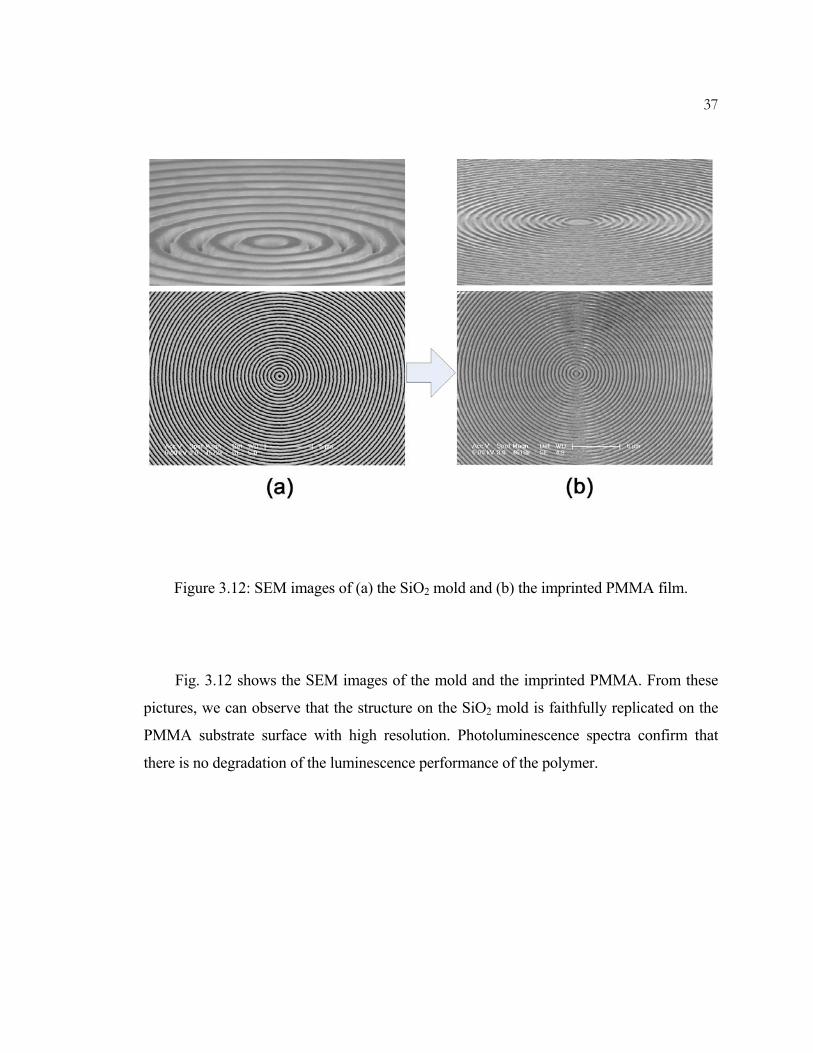
Figure 3.12: SEM images of (a) the SiO2 mold and (b) the imprinted PMMA film.
Fig. 3.12 shows the SEM images of the mold and the imprinted PMMA. From these
pictures, we can observe that the structure on the SiO2 mold is faithfully replicated on the
PMMA substrate surface with high resolution. Photoluminescence spectra confirm that
there is no degradation of the luminescence performance of the polymer.
38
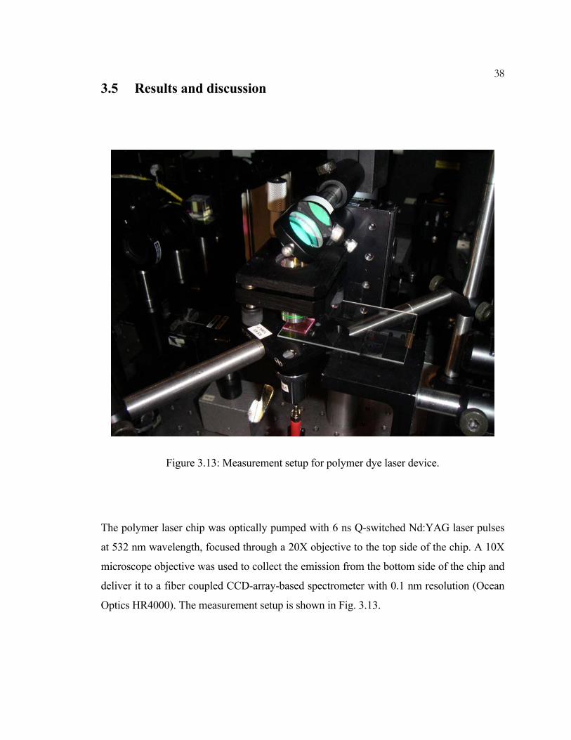
3.5 Results and discussion
Figure 3.13: Measurement setup for polymer dye laser device.
The polymer laser chip was optically pumped with 6 ns Q-switched Nd:YAG laser pulses
at 532 nm wavelength, focused through a 20X objective to the top side of the chip. A 10X
microscope objective was used to collect the emission from the bottom side of the chip and
deliver it to a fiber coupled CCD-array-based spectrometer with 0.1 nm resolution (Ocean
Optics HR4000). The measurement setup is shown in Fig. 3.13.

39
590 595 600 605 610 615 620 625 630 6350
0.1
0.2
0.3
0.4
0.5
0.6
0.7
0.8
0.9
1
Wavelength (nm)
No
rma
lize
d In
ten
sity
(a
.u.)
FWHM=0.18nm
Figure 3.14: Nanoimprinted circular grating DFB dye laser spectrum. The measured
linewidth is 0.18 nm. Inset: Polymer laser chip excited by Nd:YAG 532 nm laser pulse.
A typical single-frequency lasing spectrum is shown in Fig. 3.14. The lasing
wavelength is 618.52 nm, and the measured linewidth is 0.18 nm. Lasing occurs near the
Bragg resonance, determined by the equation effBragg nm 2 , where 2m is the order
of diffraction, effn is the effective refractive index of the propagation mode, and is the
grating period. The linewidth near threshold is measured as 0.20 nm, which results in a
cavity quality factor (Q) of over 3000.

40
30 40 50 60 70 80 90 1000
5
10
15
20
25
30
35Threshold Fluence: 1.31 J/mm2
Absorbed pump Energy (nJ)
Out
put L
aser
Pow
er (
W)
Figure 3.15: The output laser power vs. the absorbed pump energy curve. The threshold
pump fluence is 1.31 μJ/mm2.
Fig. 3.15 shows the variation of the output laser power as a function of absorbed pump
energy. With the absorbed threshold energy of 41.3 nJ, the threshold pump fluence is
estimated to be 1.31 μJ/mm2. This pump intensity is well within the reach of commercial
high power blue laser diodes (LDs), enabling a self-contained LD pumped device. The
polymer laser is pumped from the surface of the chip and the lasing emission is collected
from the back side of the chip. The transparency of the substrate, the size and geometry of
the laser cavity, and the low threshold match well with the output beams of high power
LED and LD. Therefore the replication-molded ring geometry represents a very promising
structure for the construction of compact LED or LD pumped portable dye lasers.

41
Figure 3.16: (a) Far-field image of the emission pattern recorded by a CCD camera. (b)
Circular grating DFB laser far-field radiation patterns through a linear polarizer with
different orientation angles. The laser emits an azimuthally polarized, well-confined
circular beam.
Fig. 3.16 (a) represents the far-field image of the emission pattern recorded by a CCD
camera, and Fig. 3.16 (b) shows the far-field radiation patterns of the laser passing through
a linear polarizer with different orientation angles. The laser is expected to be azimuthally
polarized [31], as illustrated in the polarization patterns. The azimuthal polarization also
results in a zero electrical field (a dark spot) at the center of the laser [26]. In the lasing
process, many spatial modes can be excited with their mode thresholds very close to each
other [7]. The fundamental mode is normally the favored one, because higher order modes
do not overlap well with the gain region.

42We observe decreases in the laser emission with increasing exposure time. This
result is consistent with previous studies on polymer DFB structures [32]. The lifetime of
polymer dye laser can last over 106 shots of pump laser pulse, and if the characterization of
the device is carried out under vacuum to inhibit photo-oxidation, the lifetime can be
further extended [33]. Because of the low cost of materials and fabrication, replication
molded devices are disposable and may not require a long lifetime. In the future, we plan to
make an optofluidic version [34, 35] of the circular grating dye laser which allows us to
constantly change the dye to increase the device lifetime and to tune the wavelength [36].
3.6 Summary
In summary, we have demonstrated a surface emitting polymer dye laser with a circular
grating distributed feedback structure realized by nanoimprint lithography. We have
achieved excitation thresholds as low as 1.31 μJ/mm2 and FWHM linewidths of 0.18 nm.
The technique described here enables the fabrication of low cost, high quality and mass
producible laser arrays, which may be deployed as compact and inexpensive coherent light
sources for lab-on-a-chip applications such as sensing and spectroscopy. Future work will
be focused on improving the laser cavity Q values with better electromagnetic design,
optimizing the dye concentration, and fabricating smoother surfaces. The ultimate goal is to
reduce the lasing threshold to enable the use of LEDs as integrated and inexpensive pump
sources for on-chip polymer lasers.

43
Chapter 4
Optofluidic circular grating dye laser
4.1 Introduction
The field of optofluidics, which is the integration of optics and microfluidics, has attracted
great interest for its novel implementation in biotechnology [37]. Among the new class of
optofluidic devices, On-chip liquid dye lasers allow the integration of coherent light
sources with other microfluidic and optical functionalities, and provide possibilities for
building more complete “lab-on-a-chip” systems. These optically pumped devices consist
of microfluidic channels with an embedded optical resonator, and a liquid laser dye is used
as active gain medium.
There are many unique properties of the miniaturized liquid dye lasers in microfluidic
systems. First, compared to solid-state dye lasers, the liquid gain medium in microfluidic
dye lasers makes the changing of dye easier, which is very helpful for improving the lasing
performance. For example, the photo-bleaching of the dye is significantly reduced by a
regenerating flow of dye through the lasing cavity inside the microfluidic channel. Second,
the microfluidic circuits include valves, and pumps allow the mixing of different solvents
with dyes. Therefore, the tuning of lasing wavelength can be achieved by modifying the
refractive index of the dye solution or changing the dye concentration. Third, the flexibility
and versatility of microfluidic fabrication enables the large-scale integration of laser arrays
in compact devices with more functionality. All these advantages make it possible to build

44on-chip tunable coherent light sources useful for many applications in biochemical
analysis, such as laser-induced fluorescence and spectroscopy.
Distributed feedback (DFB) laser resonators have been proven to be particularly
suitable for optofluidic devices because of their low threshold lasing operation features. A
DFB microfluidic dye laser was first demonstrated by Balslev et al. [38] who used a
high-order Bragg grating in an 8 μm thick polymer film to obtain feedback. Single-mode
lasing with a threshold fluence of approximately 20 μJ/mm2 was obtained due to mode
selective losses in the multimode structure where light was not guided in the fluidic
segments. Li et al. [34] realized a 15th-order DFB laser using low refractive index
poly(dimethylsiloxane) (PDMS) and a high refractive index liquid core. A record low
lasing threshold fluence of 8 μJ/mm2 was obtained. Gersborg-Hansen et al. realized a
third-order distributed feedback laser fabricated in a poly(methylmethacrylate) (PMMA)
integrated microfluidic device [35].
The tuning of lasing wavelength is also an attractive feature of optofluidic dye lasers.
Galas et al. have demonstrated the integration of PDMS-based microfluidic circuits with
microfluidic dye lasers to tune the laser wavelength [39]. Tunable output in microfluidic
dye laser by changing index and concentration was also investigated by Gersborg-Hansen
et al. [36]. Li et al. reported a mechanically tunable dye laser [40]. Vezenov et al.
fabricated an edge emitting dye laser in PDMS based on a liquid-liquid (L2) waveguide
and studied its lasing tuning range [41].

45
Figure 4.1: Schematic diagram of an optofluidic circular grating dye laser chip.
In this chapter, we present a surface emitting optofluidic dye laser with circular
grating distributed feedback (DFB) structure. We choose the circular grating DFB structure
as the laser cavity to achieve low-threshold, high-efficiency operation, and vertical
emission out of the device plane. The schematic diagram of our microfluidic circular
grating dye laser is shown in Fig. 4.1. The laser chip is a hybrid microfluidic device made
of poly(dimethylsiloxane) (PDMS) and perfluoropolyether (PFPE). A microfluidic channel
with the circular grating structures embedded is filled with dye solutions. The gain medium
is a 2 mM solution of Rhodamine 6G in a benzyl alcohol and methanol mixture with
refractive index of 1.53. The PDMS forms the microfluidic channel and serves as the upper
cladding of the cavity. The lower cladding material is PFPE, which also forms the circular
grating that provides the feedback necessary for the laser action.
46
4.2 Materials
4.2.1 PDMS
The most commonly used polymer in soft lithography to make microfluidic devices is
poly(dimethylsiloxane) (PDMS). PDMS is a silicone elastomer and has many advantages
for making microfluidic devices. It is optical transparent in a broad range of spectra (240
nm–1100 nm). It can be used to fabricate nanoscale structures by simple replica molding
technique because of its high elasticity and intrinsically low adhesion properties [42], and it
has easy and superior bonding property to many materials [43]. Also PDMS is low cost (~
$20/kg), biocompatible, and safe to use [44].
The PDMS replication molding process is usually composed of three steps: (1)
pouring or spin coating of PDMS prepolymer onto the structured master, (2) thermal curing
to cross-link the polymer, (3) peeling-off of cured PDMS from the master. The structured
PDMS can be utilized in a further process through bonding with other plates, such as
silicon, glass, plain PDMS, and other structured PDMS.
Soft lithography is currently the most useful technique for patterning 500 nm or larger
features [45]. However, the replication resolution is limited by the most commonly used
PDMS formulation (Sylgard 184, Dow Corning) due to several reasons. First, its low
Young’s modulus (~ 1.5 Mpa) caused high aspect ratio features to deform or collapse [46].
Second, its surface energy (~ 22–25 mN m-1) is not low enough for fabrication that requires
high fidelity [47]. Third, its poor solvent resistance leads to a swelling issue when exposed
to most organic solvents [48].
Several variants of PDMS such as h-PDMS [49] and hν-PDMS [50], have been
reported to improve the resolution and fidelity in soft lithography. The h-PDMS with short
cross-linkers has a relatively high modulus (~ 9 MPa), but its elongation at break is much
lower than that of 184-PDMS. It can be used effectively by a composite bilayer patterning
method. The combination of a thin layer of h-PDMS with a thick backing of 184-PDMS

47successfully improved the replication resolution down to 50 nm [46]. The hν-PDMS is a
photocurable version of PDMS with a modulus of ~ 4 MPa; the photopatterning in
nanostructure fabrication prevents the distortion during the thermal curing process.
hν-PDMS is easier to handle since its elongation at break is much higher than that of
h-PDMS, and it can also achieve the patterning of high aspect ratio, submicron features.
There are also other ways to improve the resolution of replication molding for
184-PDMS. The use of 184-PDMS as high-resolution mold material was reported by
Bender et al. [51], the resulting PDMS reached a modulus of ~ 3 MPa and a surface
hardness of 50 Shore A. The resolution can be further increased by a pressure-assisted
molding [52] or a diluted PDMS material [53]. However, these processes require baking of
PDMS at 130 °C, which fully cures the PDMS and prevents its further bonding with
another PDMS layer, and therefore is not advantageous for our optofluidic dye laser device
fabrication.
4.2.2 PFPE
The photocurable perfluoropolyether (PFPE) has been reported by DeSimone et al. as an
alternative material for microfluidic devices [54] and nanoimprint lithography [47]. This
(PFPE-DMA) has a modulus of ~ 4 MPa and a very low surface energy (~12 mN m-1).
More importantly, this material is solvent resistant and chemically robust to most organic
solvents. These characteristics are very attractive for the fabrication of microfluidic devices
that require higher fidelity pattering and more functionality. The main problem with the
PFPE is the fact that it is hard to bond two layers of PFPE. By adding different terminal
chemical groups to the layers that tend to react with each other, some improvement was
achieved in the bonding. However, the synthesis of this fluoropolymer is very complicated
and the yield is usually low, the small quantities of PFPE have prevented us from extensive
testing of this polymer.
48The use of a commercially available form of PFPE (CN4000, Sartomer Company,
Inc., MW=1000 g mol-1) is reported by Trong et al. [55]. This PFPE is a fluorinated
acrylate oligomer which has the backbone of fluorinated polyether with acryloxy
(CH2=CH−COO−) as ending functional groups instead of methacryloxy groups in the
reported PFPE-DMA. This material is cross-linked under UV illumination to form an
elastomer with a high modulus (10.5 MPa), a low surface energy (18.5 mN m-1), and a low
refractive index (1.341).
With the higher young’s modulus of the PFPE, we can achieve replication of higher
resolution and higher aspect ratio features, which give rise to the optical confinement of the
grating structure. The refractive index of PFPE (n=1.341) is even lower than that of PDMS
(n=1.406), which makes it more suitable to serve as a cladding material for our laser
device.
However, the bonding of PFPE remains a problem. Experiments have been conducted
to test the bonding by partially curing the material, but the results are not very promising.
Also the PFPE is too brittle to punch holes through, unlike PDMS. All these disadvantages
of PFPE prevent it from being used in simple and conventional multilayer soft lithography
to make microfluidic devices.
To successfully fabricate microfluidic channels with the sub-200 nm laser cavity
structures embedded, we not only expect the soft lithography material to have high
replication resolution, but also require a superior bonding property of the material.
Therefore, our optofluidic dye laser is composed of two layers, a stiff layer (PFPE)
supported by a flexible layer (PDMS). This composite bilayer patterning method combines
the most attractive features of both materials, and it is very useful in defining functional
microfluidic devices with nano-scale optical structures embedded.

494.2.3 Laser dye and solvents
The organic laser dye we use in the laser device is Rhodamine 6G, which is also known as
Rhodamine 590 Chloride (Exciton). The molecule structure of Rhodamine 6G is depicted
in Fig. 4.2. Use of this dye as amplifying medium in lasers is very common due to its large
quantum efficiency and relatively long lifetime against bleaching. It is extensively used in
tunable lasers in the visible wavelength for many applications, such as spectroscopy. There
are other dyes in the Rhodamine family with different wavelength, such as Rhodamine B
and Rhodamine 101. We chose Rhodamine 6G to match its absorption peak with the cavity
resonant frequency. The stimulated singlet state absorption and emission cross sections are
illustrated in Fig. 4.3.
Figure 4.2: Rhodamine 6G molecule structure.
Figure 4.3: Cross sections of stimulated singlet state absorption and emission for
Rhodamine 6G in ethanol.

50Because of the swelling issue of PDMS for most organic solvents [48], the choice of
the solvents for the dye molecules is very limited. The commonly used dye laser solvents
which are also compatible with PDMS are listed below: methanol, water, ethanol, ethylene
glycol, glycerol, dimethyl sulfoxide (DMSO), and benzyl alcohol. Table 4.1 shows the
refractive indices of these organic solvents. The available refractive index range is from
1.33 to 1.54. To obtain the highest refractive index contrast, we used a 20:1 mixture of
benzyl alcohol and methanol which has a refractive index close to 1.53. The addition of
methanol is mainly to assist the dissolving of the dye molecules. The PDMS-compatible
solvents can be mixed to produce laser dye solvents with different refractive indices, thus
providing a convenient way to achieve wavelength tuning in optofluidic devices.
Table 4.1: Refractive indices of PDMS-compatible solvents
Solvent Refractive Index* Methanol 1.33 DI Water 1.333 Ethanol 1.36
Ethylene Glycol 1.43 Glycerol 1.473 DMSO 1.478
Benzyl Alcohol 1.54 *At room temperature, sodium D line 589.3 nm

51
4.3 Laser cavity design
4.3.1 Circular grating distributed feedback structure
Figure 4.4: General design of an optofluidic circular grating DFB dye laser cavity.
The circular grating distributed feedback (DFB) structure used in our optofluidic devices is
basically the same as the one in the nanoimprinted solid-state dye lasers. Instead of doping
the dye molecules in the resonator structure, laser dye is dissolved in the organic solvents.
Fig. 4.4 shows a general design of an optofluidic circular grating DFB dye laser cavity. The
upper cladding and the lower cladding is PDMS (n=1.406) and PFPE (n=1.341),
respectively.
The circular grating structure provides a natural 2-D extension of the basic DFB
structure. The corrugations in the grating structure provide both distributed feedback and
output coupling of the guided optical mode. Theoretical analysis of circular grating lasers
predicts that only the radial propagating components define the modes in the circularly

52symmetric grating. Second-order gratings are used to obtain surface emission, because
the first-order Bragg reflection from a second-order grating can phase match radially
propagating waves to vertically propagating plane waves, as illustrated in Fig. 4.5.
Figure 4.5: Illustration of the Bragg diffraction in the second-order circular grating.
First-order Bragg reflection induces coupling to vertical propagating waves, and
second-order Bragg reflection leads to in-plane feedback.
The design parameters of the circular gratings fabricated are selected based on
electromagnetic mode calculations and experimental results. Grating periods varying from
400 nm to 440 nm are chosen to match the second-order Bragg condition. We use a deeper
grating trench to compensate for the low refractive index contrast between the dye solution
and the cladding. The 600 nm groove depth is defined to ensure maximum confinement,
whereas the 200 μm overall diameter of the circular grating and the 50% duty cycle are
used to reach the maximum coupling strength.
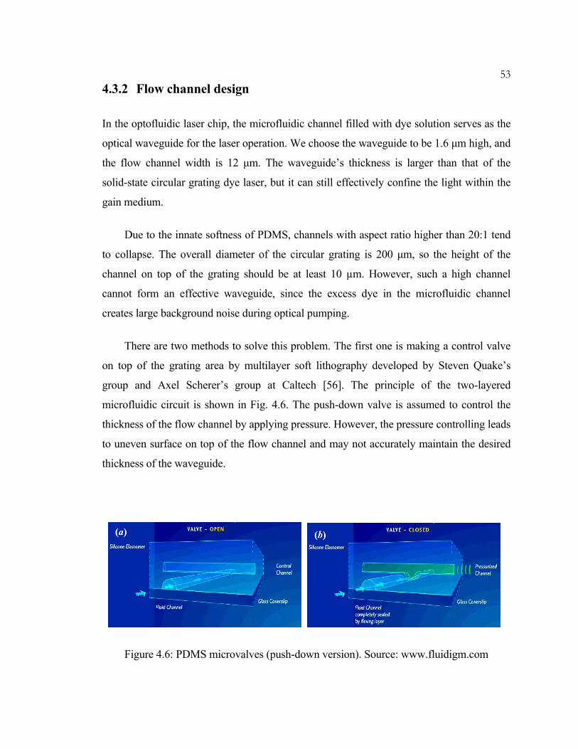
534.3.2 Flow channel design
In the optofluidic laser chip, the microfluidic channel filled with dye solution serves as the
optical waveguide for the laser operation. We choose the waveguide to be 1.6 μm high, and
the flow channel width is 12 μm. The waveguide’s thickness is larger than that of the
solid-state circular grating dye laser, but it can still effectively confine the light within the
gain medium.
Due to the innate softness of PDMS, channels with aspect ratio higher than 20:1 tend
to collapse. The overall diameter of the circular grating is 200 μm, so the height of the
channel on top of the grating should be at least 10 µm. However, such a high channel
cannot form an effective waveguide, since the excess dye in the microfluidic channel
creates large background noise during optical pumping.
There are two methods to solve this problem. The first one is making a control valve
on top of the grating area by multilayer soft lithography developed by Steven Quake’s
group and Axel Scherer’s group at Caltech [56]. The principle of the two-layered
microfluidic circuit is shown in Fig. 4.6. The push-down valve is assumed to control the
thickness of the flow channel by applying pressure. However, the pressure controlling leads
to uneven surface on top of the flow channel and may not accurately maintain the desired
thickness of the waveguide.
Figure 4.6: PDMS microvalves (push-down version). Source: www.fluidigm.com

54
Figure 4.7: Microscope graph of microfluidic flow channel. Left: flow channel covering the
grating area. Right: flow channel filled with dye solution.
The other way to make a 1.6 μm high channel over a 200 μm diameter area is more
simple and straightforward. Support pillars were fabricated within flow channels to avoid
bowing of the extremely wide PDMS channels. Fig. 4.7 shows a microscope graph of
microfluidic flow channel with little posts (5 μm diameter) fabricated inside. The spacing
between posts is around 30 μm to ensure the proper aspect ratio in between posts. Although
the channel aspect ratio (1.6:200) highly exceeds the allowed range (1:20), the flow
channel does not collapse and can be filled with dye solution. Since the height of the flow
channel is relatively small, the flow rate of the dye solution in the channel is reduced, but it
is still enough for the circulation of dye during lasing operation.

55
4.4 Fabrication process
4.4.1 Mold fabrication
To define our circular grating structure, silicon dioxide (SiO2) was used as the mold
material. In order to obtain a deep, steep-sided grating profile, we chose a deep reactive ion
etching (DRIE) process to etch SiO2. DRIE is a highly anisotropic etching process for
creating deep trenches in substrates with relatively high aspect ratio. The DRIE etching in
SiO2 requires the use of higher selective material, i.e., the Cr, as the etching mask.
The original wafer was 1 μm of SiO2 on top of Si substrate. First, 20 nm of Cr was
evaporated on the wafer using a thermal evaporator, then 2% 950K PMMA was spun on
top of the Cr layer for 1 min at 3000 rpm and baked for 15 min at 170 °C, which formed a
100 nm thick resist layer. The grating pattern was defined by electron beam lithography on
a LEICA EBPG 5000+ e-beam writer at 100 keV and 900 μC/cm2 with proximity
correction. Development of patterned PMMA film was carried out in a 1:3 MIBK:IPA
(methyl isobutyl ketone and isopropanol alcohol) solution for 1 min. Next, the wafer was
immersed in chromium etchant (CR-7, Cyantek) for 10 s to remove the Cr underneath the
exposed PMMA pattern. The remaining PMMA was removed by methylene chloride.
The pattern was subsequently transferred from Cr into SiO2 substrate via deep reactive
ion etching (DRIE) using C4F8. The SiO2 etching rate in the C4F8 DRIE process is 5 nm per
second. The schematic fabrication procedure for the soft lithography hard mold is
illustrated in Fig. 4.8.

56
Figure 4.8: Schematic fabrication procedure for the circular grating hard mold. (a) The
original wafer with 1 µm SiO2 on top of Si substrate. (b) Cr is evaporated on the sample. (c)
PMMA is spun on top of the Cr for subsequent e-beam lithography steps. (d) The PMMA
is exposed by e-beam, and the circular grating pattern is completely transferred into
PMMA after developing the exposed resist. (e) The Cr underneath the exposed pattern is
removed by wet etch, and the remaining PMMA is also removed. (f) The pattern is
transferred into the SiO2 via DRIE etch.

57
Figure 4.9: The SEM images of the cross section of etched SiO2 gratings. (a) A cut-away
view of the gratings. (b) Deeply etched trenches in the circular grating structure.
The SEM image of the cross section of etched SiO2 gratings is shown in Fig. 4.9. (a) is
a cut-away view of the gratings indicating an excellent anisotropic profile with a depth of
600 nm; (b) shows the deeply etched trenches with vertical and smooth side walls in the
(a)
(b)

58circular grating structure. The SEM images of both the top view and the angled view of
an etched SiO2 mold of circular grating are shown in Fig. 4.10.
Figure 4.10: SEM images of (a) the top view and (b) the angled view of the SiO2 mold.
(a)
(b)

594.4.2 Laser chip fabrication
The optofluidic dye laser device is fabricated by conventional multilayer soft lithography
techniques. The chip consists of two layers, the grating layer and the flow layer. The
grating layer is made of PFPE supported by a flexible PDMS backbone, and it is bonded to
the thin layer of PDMS with flow channels inside.
In our experiments, we used a commercially available form of PFPE. It is a 1 wt%
mixture of a photoinitiator, Darocurr 4265 (Ciba Specialty Chemicals), and a fluorinated
acrylate oligomer, CN4000 (Sartomer Company, Inc., MW=1000 g mol-1). Mixing the two
chemicals for 2 hours followed by filtering the mixture through a 0.22 μm syringe filter
produced a photocurable liquid resin. Exposing the material the under UV (365 nm) for 1
hour cured the material.
The fabrication of the hybrid material laser chip started with aligning a thin PDMS
layer on top of the grating mold to cover most of the mold except the grating areas. Then
the PFPE was spincoated (2000 rpm for 1 min) on the mold, followed by UV exposure for
1 hour to cure the material. After peeling of the thin PDMS layer, a new PDMS prepolymer
(5:1 RTV A:B) was poured onto the PFPE layer and degassed in a vacuum chamber for 30
min, then the prepolymer was partially cured at 80 °C for 30 min. This process formed a
support layer for the composite PFPE/PDMS structure. The PFPE/PDMS layer was peeled
from the grating mold and bonded to another PDMS layer with the flow channel. Finally,
the device was baked at 80 °C for 3 hours to ensure bonding between the two layers. The
bonding between PFPE and PDMS is not very strong, but the adhesion is sufficient for the
laser chip operation. The fabrication process of the hybrid PFPE/PDMS laser chip is
illustrated in Fig. 4.11.

60
Figure 4.11: Fabrication process of the hybrid PFPE/PDMS laser chip.
The SEM images of SiO2 mold with circular grating structure and its replica in PFPE
are shown in Fig. 4.12. The image of PFPE was obtained using an environmental SEM
(ESEM) operating at a water vapor pressure of 0.98 Torr in the chamber, and an
accelerating potential of 5 kV, in order to mitigate charging effects from the nonconductive
polymer samples. From the ESEM image we can see that the structure on the SiO2 mold is
faithfully replicated on the PFPE with high resolution, and there is no lateral collapse
between the grating lines even with aspect ratios above 3:1.

61
Figure 4.12: (a) SEM images of SiO2 mold. (b) ESEM images of PFPE replica.

62
4.5 Results and discussion
Figure 4.13: Measurement setup of optofluidic dye laser chip.
The optofluidic dye laser chip was optically pumped with 6 ns Q-switched Nd:YAG laser
pulses at 532 nm wavelength, focused through a 20X lens to the top side of the chip. A 10X
microscope objective was used to collect the emission from the bottom side of the chip and
deliver it to a fiber coupled CCD-array based spectrometer with 0.3 nm resolution (Ocean
Optics USB2000). The fluidic control tubing connected to a pressure source was used to
circulate the dye solution in the flow channel. The measurement setup of optofluidic dye
laser chip is shown in Fig. 4.13.
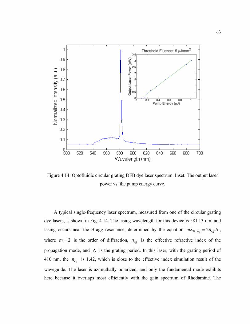
63
Figure 4.14: Optofluidic circular grating DFB dye laser spectrum. Inset: The output laser
power vs. the pump energy curve.
A typical single-frequency laser spectrum, measured from one of the circular grating
dye lasers, is shown in Fig. 4.14. The lasing wavelength for this device is 581.13 nm, and
lasing occurs near the Bragg resonance, determined by the equation effBragg nm 2 ,
where 2m is the order of diffraction, effn is the effective refractive index of the
propagation mode, and is the grating period. In this laser, with the grating period of
410 nm, the effn is 1.42, which is close to the effective index simulation result of the
waveguide. The laser is azimuthally polarized, and only the fundamental mode exhibits
here because it overlaps most efficiently with the gain spectrum of Rhodamine. The

64optofluidic dye laser is pumped from the surface of the chip, and the lasing emission is
collected from the back side of the chip.
The inset shows the variation of the output laser power as a function of pump energy,
the threshold pump fluence is estimated to be 6 μJ/mm2. This relatively low pump
threshold is within the reach of high power laser diodes operating in pulsed mode. In order
to realize light-emitting diode pumped optofluidic dye lasers, however, further reduction of
the dye laser threshold is required. The small size and surface emitting geometry of the
laser cavity also provide a simple but efficient scheme to construct laser arrays with
geometrically controlled emission wavelengths, pumped with a single wavelength source.
The decrease in the laser emission with increasing exposure time was observed during
laser operation. Since the typical photo-bleaching time of Rh6G is ~ 50 ms under pump
intensities required for laser threshold (~ 100 kW/cm2), circulating the dye solution with an
appropriate flow rate prevents the dye molecules from photo-bleaching under pulse
operation. Therefore, the optofluidic version of the circular grating dye laser allows us to
constantly change the dye to increase the device lifetime.
Due to the small size (~ 200 μm) of the laser geometry, it is convenient to construct
laser arrays with different grating periods in the same chip. The whole chip can be excited
simultaneously to achieve parallel operation of the laser arrays. The grating periods vary
from 400 nm to 440 nm with a spacing of 5 nm so that the resulting lasing wavelengths are
within the gain spectrum of the laser dye Rhodamine 6G. Different laser dyes with
separated absorption peaks can also be introduced in multiple flow channels to expand the
emission spectral range.
The microfluidic compatibility of the laser chip also suggests that we can achieve
wavelength tuning by mixing two solvents with different refractive indices. The mixing and
delivery of dye solutions can be implemented in a microfluidic chip using pneumatic valves
and pumps.

65
4.6 Summary
In this chapter, we demonstrate a second-order circular grating distributed feedback
structure embedded in an optofluidic dye laser system. We obtain surface emitting single
frequency lasing at a relatively low pumping threshold. To construct these circular grating
dye lasers, we have developed a hybrid PFPE/PDMS soft lithography technique that
enables the fabrication of low cost, disposable, and high quality dye laser arrays. This
polymer heterostructure also provides a convenient method for fabricating optofluidic
device with nano-scale optical structures embedded within traditional PDMS flow
channels. Parallel lasing operation and automatic wavelength tuning can also be achieved
using the microfluidic circuit. The construction of compact and inexpensive coherent light
sources fully integrated with microfluidics provides an efficient approach to realize
complete “lab-on-a-chip” systems.

66
Chapter 5
Microfluidic device as a platform for single cell biochemical analysis
5.1 Introduction
5.1.1 Microfluidic device as a platform for biochemical analysis
Over the decade of its existence, the rapid development of polydimethylsiloxane
(PDMS)-based microfluidics and its components have found many useful applications in
biotechnology. The now-established techniques in microfluidics not only include
microchannels with pneumatic valves, pumps, mixers, and other specialized structures,
but also enables large-scale-integration of thousands components in a single chip. There are
many successful applications in biochemistry, such as cell sorting and cytometry, nanoliter
PCR, protein crystallization, DNA sequencing, nucleic acids extraction and purification,
immunoassays, cell studies, and chemical synthesis.
In this chapter, we focus on how to use microfluidic systems to extract gene
expression information on single cells. Microfluidic devices fabricated by multilayer soft
lithography possess the ability to manipulate fluids on the nanoliter scale. Therefore, they
provide an ideal platform to improve single-cell gene expression profiling by manipulation
of a single cell in nanoliter reactions. Cells can easily be isolated in a high-throughput
manner, with highly concentrated cDNA being generated using a solid phase synthesis

67approach. Then the cDNA can be extracted and realtime quantitative PCR can be
performed outside of the chip to amplify the target genes and measure their molecule
numbers.
5.1.2 Significance of single-cell gene analysis
The fundamental challenge for stem-cell gene expression study is that stem cells are
extremely rare in the context of numerous differentiated and mature cells, and there is no
definitive marker for the isolation of a homogenous pure stem cell population. There is
especially a lack of markers to distinguish closely related stem cells and progenitor cells.
Many stem-cell gene expression profiling studies have by default used heterogeneous
populations of stem cells and progenitor cells. Data obtained from these
population-averaging expression profiles reflect the sum of all the subpopulations. Without
knowing the relative percentages of stem cells and progenitor cells in the interrogated
population, these gene expression profiles, which are the sum of all expression profiles
from various cell types, are very difficult to interpret and not sufficiently informative. Even
if the percentages are known, variation in the expression profiles among individual stem
cells in different phases of the cell cycle would not be detectable by these current methods.
Single-cell transcriptome analysis can overcome this hurdle and provide precise
information on stem cell gene regulation as revealed in individual, separately analyzed
cells.
Single-cell gene expression profiling from early embryos has suggested the transient
expression of critical regulatory genes, again underscoring the importance of systematical
single-cell expression profiling [57, 58]. Currently, multiple-color florescent-activated cell
sorting (FACS) has limited utility for isolation of pure stem cell populations due to a lack
of discriminating cell markers. Single-cell gene expression profiling studies with laser

68capture microdissection (LCM) [59-68], patch-clamp analysis [58, 69, 70], and in situ
mRNA amplification [69, 71] have been reported, but analysis of a large number of cells
has proven to be very difficult with these methods. Single-cell whole genome microarray
gene expression screening [60, 61, 72] and single-cell cDNA library construction [57, 73,
74] also have been conducted on a limited number of cells. While these studies demonstrate
the potential value of single-cell gene expression profiling, they also show the limitation of
these methods when processing a large number of samples. Material loss and low
biochemical reaction efficiency (mRNA capture and RT reaction) are other major
challenges for single-cell analysis. A single mammalian cell contains 20–40 pg of total
RNA [75, 76], but only 0.5–1.0 pg of mRNA (105 to 106 mRNA molecules) [77].
Therefore, detecting single-cell mRNA is difficult with current methods.
The microfluidic device described here significantly increases the mRNA-to-cDNA
processing efficiency ~ 5-fold to 54% compared to bulk reactions (~ 12%) [78, 79]. With
this device, we measured the absolute copy number of three genes in individual single
hESCs and compared these data to those obtained from cDNA of FACS-sorted hESCs in
G0/G1 phase. Our results indicate that the hESC colony is a heterogeneous cell population
and many single cells do not express all three of the interrogated genes. This result suggests
that pluripotent hESC colonies are not homogeneous cell populations, rather they are a
highly heterogeneous cell population regulated by different gene networks. Besides
stochastic factors of individual cells, heterogeneity of cells with respect to cell cycle and
other factors may be a major contributor to observed variations in mammalian single-cell
gene expression.

69
5.2 Design of microfluidic devices for single-cell analysis
5.2.1 First generation of microfluidic chip
Previous work which has been done by Joshua Marcus in the Quake laboratory [81]
provided a starting point for the design of a microfluidic single-cell gene analysis device.
The integrated process of cell capture/lysis, mRNA isolation/purification, and cDNA
synthesis/purification is implemented in a multilayer microfluidic chip.
Figure 5.1: 20X single-cell mRNA extraction microfluidic device filled with food dye.

70The first generation of microfluidic single-cell mRNA extraction microfluidic chip
is shown in Fig. 5.1. All flow channels are filled with yellow food dye, multiplexer control
channels are filled with red dye, control channels are in green dye. After loading cell
suspension from the cell input inlet, single cells are captured in cell lysis module (Inset 1)
within the flow channels (blue). The pump valves are green, the separation valve is black,
and the lysis buffer is yellow. A captured single hESC is labeled with a fluorescent dye
(green) and shown in Inset 2. Cell lysis is performed by opening the portion valve and
pumping to mix lysis buffer (yellow) with the captured cell (blue). The resulting cell lysate
is pushed through oligo-dT beads columns for mRNA capture. Oligo-dT beads are stacked
into columns by closing the sieve valve while loading bead suspension. Inset 3 shows six
stacked oligo-dT bead columns next to the sieve valve. After washing beads with buffers,
RT reaction master mix is flowed through the bead columns to synthesize cDNA from the
captured mRNA at 40 C. After RT reaction, beads with attached cDNA are pushed to
collection wells (Inset 4) by opening the sieve valve. The beads are recovered by cutting
the wells off the chips and centrifuging a flipped-well in a microcentrifuge tube.
5.2.2 Second generation of microfluidic chip
The output efficiency of the first generation of microfluidic chip is considerably low
because the cells are randomly loaded in each reaction chamber. We intend to improve the
efficiency of the gene analysis on the microfluidic platform to achieve real single-cell
analysis. In order to achieve this goal, the chip design can be changed to implant
multiplexer in both the cell loading and mRNA extraction parts of the device. Therefore,
the second generation of microfluidic chip shown in Fig. 5.2 can carry out single-cell gene
analysis in a 32X parallel manner. Although we do not greatly increase the number of cells
to be processed, efficiency of 100% of single-cell processing can be achieved by the
improved design.

71
Figure 5.2: 32X single-cell gene profiling microfluidic device filled with food dye.
In the 32X single-cell microfluidic processor, all flow channels are filled with yellow
dye, control channels are filled with green dye, multiplexer control channels are filled with
red dye, and the cell loading portion is in blue dye. First the cell suspension is flowed
through the cell loading portion, and the captured single cell can be individually pushed to
the cell lysis module (Inset 1) by operating the corresponding valve in the multiplexer
(Inset 2). 32 reactions can be carried out in one microfluidic device. Cell lysis is performed
by opening the portion valve and pumping to mix lysis buffer (yellow) with the captured
cell (blue). The resulting cell lysate is pushed through oligo-dT bead columns (Inset 3) for
mRNA capture. The following RT reaction and cDNA synthesis are the same as the
process in the previous version of microfluidic chip.

72
5.3 Materials and methods
5.3.1 Mold fabrication
All photomasks were designed with AutoCAD software, and printed at a resolution of
20,000 dots per inch on transparency films (CAD/Art services). We used both the control
mold and flow mold to define device features. The control mold with 24 um high features
was fabricated with a single step using SU8-2025 (Microchem, USA). The flow mold was
fabricated with three lithographic steps. First we defined the 10 um high column
construction flow channels with SU8-2010 (Microchem, USA). Then the 12 um high
output, bead, and buffer delivery channels were fabricated using SPR220-7 (Shipley,
USA). In addition, a hard bake process at 200 °C facilitating channel rounding was
necessary for valve closure. The last step was to construct the 40 um high cell loading
channels with AZ-50 (Clariant). In all optical lithography processes, mold exposures were
under UV light on a MA6 mask aligner.
5.3.2 Device fabrication
The microfluidic devices were fabricated by multilayer soft lithography with the silicone
elastomer polymethylsiloxane (PDMS, General Electric). Each device employs push-up
valve geometry and consists of a three-layer elastomeric structure.
The molds were first exposed to chlortrimethylsilane (TMCS, Aldrich) vapor for 2
min to promote elastomer release after the baking steps. For the flow layer of the device, a
mixture of PDMS (5 parts A: 1 part B) was poured onto a flow mold. After degassing, the
flow molds were baked for 45 min at 80 °C. For the control layer of the device, a mixture
of PDMS (20 parts A: 1 part B) was spun on the control mold at 1800 rpm and baked for
30 min at 80 °C. The flow layer was separated from the flow mold and flow channel access
holes were then punched. Next, the flow and control layers were aligned and baked for 45

73min at 80 °C. The two-layer structure was peeled from the control mold with control
channel access holes punched, and was mounted to another thin PDMS layer made by
spinning 20:1 PDMS mixture on a blank wafer. After baking for 3 hours at 80 °C, the
three-layer structure was bonded to a clean microscope slide and baked overnight at 80 °C.
5.3.3 Microfluidic station
Fig. 5.3 shows the setup of the microfluidic system. The microfluidic valves within the
device are controlled by individual pressure regulators (Fluidigm, USA) and are interfaced
via 23 gauge stainless steel tubing (New England Small Tube) and tygon tubing (VWR).
An NI-DAQ card through a Labview interface (National Instruments) was used to control
the pressure regulators.
Figure 5.3: The setup of the microfluidic device for single hESC mRNA extraction. (a) The
system includes a microscope, a computer to control air pressure with pressure regulators,
and a heating plate. (b) A typical microfluidic chip.

745.3.4 Synthesis of cDNA from hESCs
Figure 5.4: Merged image of immunofluorescent-stained (Oct-3/4) and light microscope
images from a pluripotent hESC colony. The hESC colony was labeled with mouse α
human Oct-3/4 IgG and PE-conjugated rabbit anti-mouse IgG antibodies. Only cells in the
center of the hESC colony expressed Oct-3/4.The intensity of the labeling indicates the
Oct-3/4 positive cells expressed Oct-3/4 at different levels. The spontaneous differentiated
cells around the colony do not express Oct-3/4.
Fig. 5.4 shows the human embryonic stem cell (hESC) colonies for microfluidic analysis.
The centers (100 to 200 cells) of hESC colonies from feeder-free cultures (matrigel) were
mechanically picked up with a 25 gauge needle. The cells were disassociated into
single-cell suspension with trypsin. After being labeled with a DNA-selective dye for living
cells, Vybrant DyeCycle Green (Invitrogen, USA), FACS was performed to isolate cells in
G0/G1 phase based on DNA content. These isolated cells were pooled to extract total RNA
with Trizol LS (Invitrogen, USA), or loaded into the microfluidic device for processing.
Typically, 150,000 FACS-sorted cells were pooled for Trizol RNA extraction, and 2,000 to
5,000 cells were used for microfluidic experiments. To compare the efficiency of bench-top

75bulk assays to microfluidic assay, the same biochemical reagents were used for the bulk
assay and the microfluidic device.
Single-cell lysis, mRNA capture, and RT were performed in the same microfluidic
device to convert mRNA into cDNA. Dynabeads with oligo (dT)25 (Invitrogen, USA) were
used to capture mRNA. Sensiscript RT kit (Qiagen, USA) was used for converting
captured mRNA to cDNA. The oligo (dT)25 sequence in Dynabeads serves as both mRNA
capture sequence and primer for cDNA synthesis. After oligo (dT)25 beads with attached
cDNA were flushed to the collection wells, the wells were cut off from the chip.
Centrifugation was used to transfer the beads from individual wells into PCR tubes. These
beads with attached cDNA from individual cells were subjected to realtime qPCR for
measurement of molecule numbers of interrogated mRNA in IQ5 (Bio-Rad, USA).
5.4 Operation of microfluidic device
The process flow in the single-cell microfluidic processor is shown in Fig. 5.5. The
processor captures mRNA from 20 single cells separately and simultaneously, and then
converts it into individual cDNA. The lysis buffer was loaded into the flow channels until it
reached the waste outlets, so as to leave no air bubbles in the channel. Oligo (dT)25 beads
(Invitrogen, USA) were then loaded, and columns were built serially by addressing flow
lines individually with the multiplexer control channels, while keeping the sieve valve
actuated. Once columns were built, excess beads still present in the flow channels were
flushed with the lysis buffer to the constructed columns. A single-cell suspension was then
loaded. By adjusting cell concentration and flow rate, a single hESC was captured in an
individual cell-lysis module. Cells were then lysed chemically by mixing cells with the
lysis buffer in the ~ 10 nl ring. Mixing occurred by executing a peristaltic pump sequence
[80, 81] with control channels. Cell lysates were then pushed via pneumatic pressure over
the affinity columns to captured mRNA with oligo (dT)25 beads. After washing the
columns with a first strand synthesis buffer, the reverse transcription (RT) master mix was

76introduced. Once the RT master mix filled the flow channels, first strand synthesis was
then carried out by heating the processor to 40 °C on a thermal microscope stage. The oligo
(dT)25 beads served as both primers (oligo (dT)25 sequences and a solid phase support. The
RT reaction mixture (99 ul) was flowed over the columns for 45 min until the RT reaction
was completed at a flow rate of ~ 20 μm/s. Upon completion of the RT reaction, the waste
valves were closed, and collection valves were opened. The beads were sent to collection
wells by opening the sieve valves and flowing columns of the processor in a serial manner
with a PCR buffer. The fluid multiplexer was used to push beads in each of the 20 reaction
channels individually. Beads were collected by cutting the collection wells off the device
and centrifuging the beads into PCR tubes.
Figure 5.5: The process flow in the single-cell microfluidic processor.

77
5.5 Results and discussion
5.5.1 Device efficiency
Single-cell measurement of mRNA is difficult. One difficulty results from the loss of
material during the steps of single-cell capture, lysis, mRNA isolation, and cDNA
synthesis. Unlike the DNA molecule, mRNA is very susceptible to degradation by widely
existing RNase. Therefore, it is essential to carry out the cDNA first strand synthesis on the
same device immediately after mRNA capture. Another difficulty in measurement is the
low mRNA-to-cDNA efficiency, mRNA capture (~ 40–50%) and RT reaction (~ 20%) [78,
79] in bulk assays.
In order to measure the absolute number of molecules of mRNA with standard curves,
the mRNA-to-cDNA efficiency of the processor must be obtained. An artificial Poly-A
RNA standard (Affymetrix, USA) was used to compare the input mRNA copy number to
the cDNA copy number which was measured by qPCR at the end of the processes. This
RNA standard contains known amounts of artificial RNAs with poly-A tails from 4 B.
subtilis genes, lys, phe, thr, and dap. The lys gene was used as RNA standard for
calculation of mRNA-to-cDNA efficiency. A standard curve was generated with a known
amount of lys DNA at 10-fold dilutions. The mRNA capture and RT reaction were carried
out at both conventional micro-liter level and at nanoliter scale with the microfluidic
processor.
In the conventional reaction, a 50 μl RT reaction was carried out after capturing 4 μl
of artificial mRNA (7.3 nM) with 30 μl oligo (dT)25 beads, as instructed by the
manufacturer. One microliter of the RT product (corresponding to 2.16×10⁸ molecules of
lys artificial mRNA) was used for realtime quantitative PCR (qPCR) detection. Based on
the standard curve, the final detected molecule number was 2.5+ 0.5×10⁷ molecules (Table
5.1). The processing efficiency of a conventional microliter scale reaction is 12%. To
compare the efficiency of conventional and microfluidic approaches, the same artificial
RNA sample was introduced into the cell capturing chamber, processed into cDNA and

78detected with realtime qPCR. Each of the 20 cell-capture chambers in the microfluidic
device has a volume of 3.4 nl, resulting in 1.84×10⁶ molecules of input lys artificial mRNA.
The qPCR detected absolute lys cDNA molecule number is 1.0+ 0.3×10⁶ with the
standard curve. The total processing efficiency was 54% which is approximately 5 times
the efficiency of the conventional approach. A series of 10-fold dilutions of the artificial
RNA were used and verified that the processing efficiencies of both approaches do not vary
significantly in different concentrations of the input artificial RNA. The standard deviations
of both bench-top and microfluidic reactions were also calculated and are similar (Table
5.1). The small standard deviation of the 20 reactions in the same device indicates
consistent processing efficiency among the 20 reaction chambers.
Table 5.1: Microfluidic device increasing mRNA capture and reverse transcription (RT) efficiency. Known amounts of artificial lys mRNAs in a mixture with 3 other polyA artificial RNAs were processed with traditional microliter scale reaction or with microfluidic device in nanoliter scale. A standard curve was generated with a known amount of lys DNA for the detection of cDNA molecule numbers (y = -3.5547X + 39.538 R2 = 0.99). Molecule numbers of lys cDNA were calculated from the standard curve with real-time PCR threshold cycles. Processing efficiencies were calculated by dividing the measured cDNA molecule numbers to the input mRNA molecule numbers.
Input lys RNA
(molecule umber) Threshold
Cycle Detected cDNA
(molecule number) Efficiency (%)
Microliter Reaction (Bench-top)
2.16×10⁸ 13.22+0.37
(n = 20) 2.6 + 0.6×10⁷ 12 %
Nanoliter Reaction (Microfluidic)
1.84×10⁶ 18.15+0.46
(n = 20) 1.0 + 0.3×10⁶ 54 %

79
Fzd4
y = -2.9681x + 35.733 R2 = 0.9949
B2M
y = -3.2802x + 36.531R2 = 0.9856
Nodal
y = -3.19x + 35.861 R2 = 0.9936
0
5
10
15
20
25
30
35
40
0 1 2 3 4 5 6 7
Log (molecule number)
Th
res
ho
ld c
yc
le
Fzd4
B2M
Nodal0
200
400
600
800
1000
1200
1400
1600
1800
2000
1 4 7 10 13 16 19 22 25 28 31 34 37 40 43 46 49
Thermal Cycle
Re
lati
ve F
luo
resc
ence
Un
its
B2M (Single cell)B2M (Population cDNA)Fzd4 (Single-cell)Fzd4 (Population cDNA)Nodal (Single cell)Nodal (Population cDNA)B2M (Negative)Fzd4 (Negative)Nodal (Negative)
Figure 5.6: Measuring absolute molecule numbers of three genes in single hESC with
multiplex quantitative PCR. (a) Standard curves are generated with known amounts of
plasmid DNA containing the full sequence of the genes. The curves cover from 2 to 2x10⁶
copies of the respective genes. With our primer design, all the curves overlap each other,
and indicate similar PCR efficiency. The insert is the representative amplification cures of
the B2M genes from 2 to 2x10⁶ copies in 10-fold dilution. (b) The multiplex quantitative
PCR amplification curves obtained from cDNA of hESC colonies are plotted with curves
obtained from cDNA of a representative hESC. Because the standard curves of the three
genes are very similar, these amplification curves show that the expression ratio of B2M
and Nodal is similar in population cDNA and this single-cell cDNA. However, the
expression of Fzd4 and Nodal is very similar in this particular single hESC, but very
different in the hESC population. Unlike this single hESC, some single hESC do not
express all three genes. This result suggests the heterogeneity of hESC and underscores the
importance of single-cell analysis.
(a) (b)
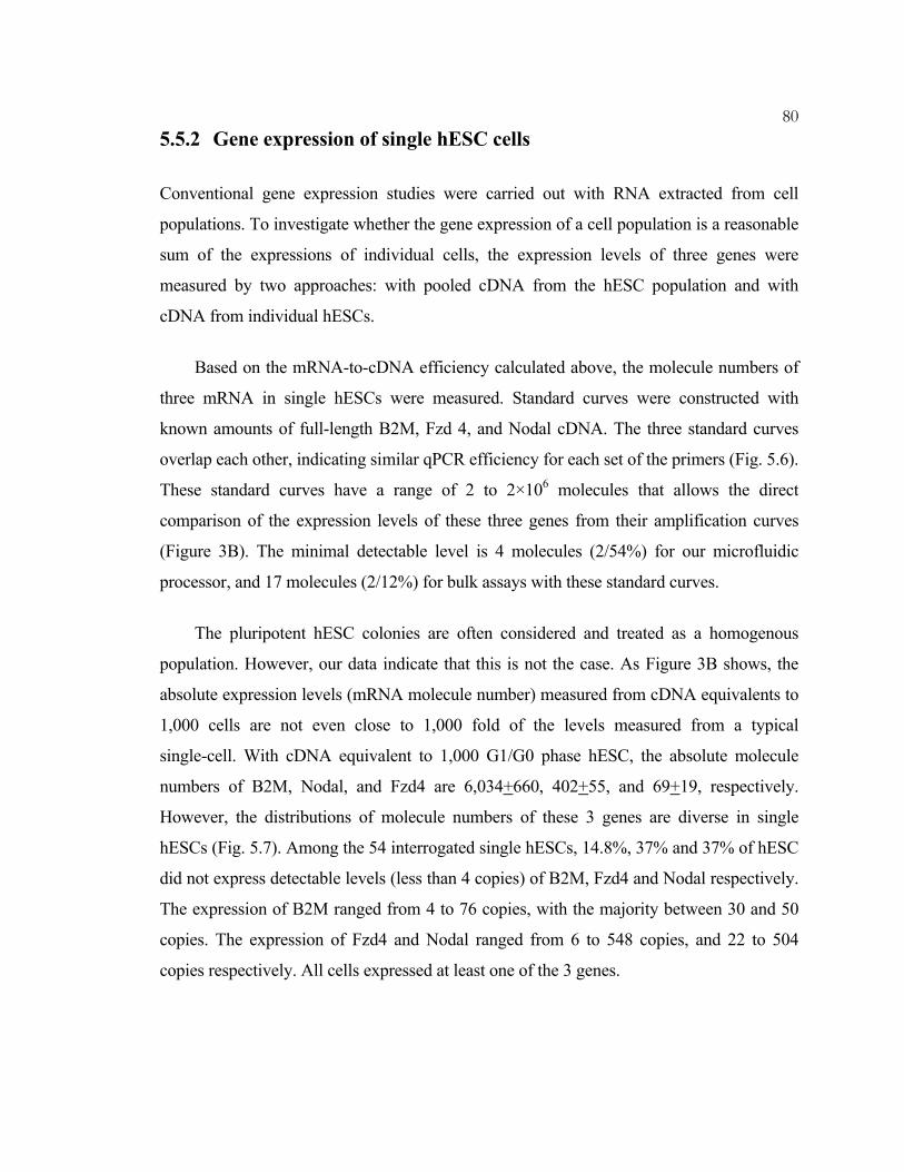
805.5.2 Gene expression of single hESC cells
Conventional gene expression studies were carried out with RNA extracted from cell
populations. To investigate whether the gene expression of a cell population is a reasonable
sum of the expressions of individual cells, the expression levels of three genes were
measured by two approaches: with pooled cDNA from the hESC population and with
cDNA from individual hESCs.
Based on the mRNA-to-cDNA efficiency calculated above, the molecule numbers of
three mRNA in single hESCs were measured. Standard curves were constructed with
known amounts of full-length B2M, Fzd 4, and Nodal cDNA. The three standard curves
overlap each other, indicating similar qPCR efficiency for each set of the primers (Fig. 5.6).
These standard curves have a range of 2 to 2×10⁶ molecules that allows the direct
comparison of the expression levels of these three genes from their amplification curves
(Figure 3B). The minimal detectable level is 4 molecules (2/54%) for our microfluidic
processor, and 17 molecules (2/12%) for bulk assays with these standard curves.
The pluripotent hESC colonies are often considered and treated as a homogenous
population. However, our data indicate that this is not the case. As Figure 3B shows, the
absolute expression levels (mRNA molecule number) measured from cDNA equivalents to
1,000 cells are not even close to 1,000 fold of the levels measured from a typical
single-cell. With cDNA equivalent to 1,000 G1/G0 phase hESC, the absolute molecule
numbers of B2M, Nodal, and Fzd4 are 6,034+660, 402+55, and 69+19, respectively.
However, the distributions of molecule numbers of these 3 genes are diverse in single
hESCs (Fig. 5.7). Among the 54 interrogated single hESCs, 14.8%, 37% and 37% of hESC
did not express detectable levels (less than 4 copies) of B2M, Fzd4 and Nodal respectively.
The expression of B2M ranged from 4 to 76 copies, with the majority between 30 and 50
copies. The expression of Fzd4 and Nodal ranged from 6 to 548 copies, and 22 to 504
copies respectively. All cells expressed at least one of the 3 genes.

81
A Single-hESC Expresses Fzd4 and Nodal
-100
0
100
200
300
400
500
600
0 5 10 15 20 25 30 35 40 45 50
Thermal Cycle
Rel
ati
ve F
luo
resc
ence
Un
its
B2M Fzd4 Nodal
A Single-hESC Expresses Nodal
-50
0
50
100
150
200
250
300
350
0 5 10 15 20 25 30 35 40 45 50
Thermal cycle
Rel
ativ
e F
luo
resc
ence
Un
its B2M Fzd 4 Nodal
Distribution of B2M in Singel hESC
0
5
10
15
20
25
30
35
40
45
Not d
etect
ed 50100
150200
250
500
Over 5
00
Distribution of Fzd4 in single hESC
0
5
10
15
20
25
30
35
40
45
Not d
etect
ed 50100
150200
250500
Over 5
00
Distribution of Nodal in Single hESC
0
5
10
15
20
25
30
35
40
45
Not d
etec
ted 50
100150
200
250500
Over 5
00
Figure 5.7 Expression of B2M, Nodal, and Fzd4 in a single hESC. (a) A single-hESC
expresses both Nodal and Fzd4, but does not express B2M in a detectable level. (b) A
single hESC expresses only Nodal. The mRNAs of B2M and Fzd4 are undetectable. (c),
(d), and (e) show the distribution of the B2M, Fzd4 and Nodal in a single hESC. Among
the 54 interrogated single hESC, 14.8%, 37%, and 37% of cells (indicated by black strait
pattern) do not express detectable levels (less than 4 copies) of B2M, Fzd4, and Nodal,
respectively. The distribution pattern of expressions is narrower in B2M compared to the
other 2 genes. The discontinued distribution of Nodal and Fzd4 suggest a high
heterogeneity of the 54 cells.
(b)
(c) (d) (e)
(a)

82
Many gene expression studies, such as microarray or quantitative PCR, are based on
the relative expression level of genes with normalization to a housekeeping gene which is
assumed to have similar expression in all samples. Our data show that even the relative
expression level of the three genes are very different between measurements derived from
cDNA of a cell population and separately from individual cells. In the measurement from
population cDNA, the expression level of Fzd4 is approximately 8-fold lower than the
expression of Nodal after being normalized to B2M. However, in a representative single
hESC, the expression levels of Nodal and Fzd4 are very similar after normalization with
B2M (Fig. 5.7).
5.6 Conclusions
Microfluidic devices that are designed to manipulate nanoliter amounts of reagents provide
a desirable platform for single-cell gene expression processing. As our data indicate,
capturing mRNA and converting it to cDNA in a microfluidic device not only consumes
significantly less reagents, but most importantly increases the efficiency of biochemical
reactions. The microfluidic device described has a mRNA-to-cDNA efficiency 5 times
better than the corresponding bench-top reactions. Previous studies showed a 40–55%
mRNA capture efficiency of oligo (dT)25 [78], and ~ 20% RT efficiency [79] in
conventional bench-top reactions. The 12% overall efficiency of our bulk assay is
consistent with these previous studies (55% × 20%). With our microfluidic device, the
mRNA-to-cDNA processing efficiency is 54% (5-fold better than bulk assay). This finding
indicates a very efficient mRNA-to-cDNA processing that may be due to the nanoliter scale
reaction. This mRNA-to-cDNA efficiency is similar to the previously reported efficiency
from other microfluidic devices [82].

83Due to the nanoliter scale nature of the microfluidic device, the input number of
mRNA in conventional reaction and microfluidic reaction is ~ 100-fold different when the
same RNA standard is used. To rule out the possibility of RNA concentration in processing
efficiency, serial 10-fold dilutions of the RNA standard were used for the same
experiments. The mRNA-to-cDNA efficiencies are not significantly different for either
bench-top or microfluidic reactions. Therefore, the high mRNA-to-cDNA efficiency is a
desirable characteristic of microfluidic devices. With this 54% processing efficiency, the
microfluidic device described potentially can detect 2 mRNA copies of interrogated genes.
In our device, there are 20 individual single-cell processing reactors for
simultaneously processing. The standard deviation of threshold cycles of the 20 reactors is
small (0.37) and similar to those from conventional reactions (~ 0.5). These data indicate
that the processing efficiencies among the 20 reactors are very similar. Similar results are
also obtained in multiple lots of devices. This aspect is critical for comparing results from
individual cells intra- and inter-device.
With this device, we profiled the expression of three genes in hESC. Our data
indicated that even for FACS-sorted G1/G0 phase hESC, the expression data from
population cDNA can not be used to estimate the gene expression level in individual cells.
Approximately 10–15% of individual cells do not express one of the three interrogated
genes. Therefore, the population averaging effect distorts the expression levels of the three
genes in bulk assays conducted with population cDNA from hESC colonies. Because the
population averaging effects are not the same for all three genes, the relative expression
levels are also distorted. The qPCR with cDNA from 1,000 hESC indicates that Nodal is
expressed approximately 8 times higher than Fzd4 after normalization to B2M. However,
in individual cells the expressions of these genes are very diverse. The difference observed
in pooled cDNA may be due to the different number of cells expressing the respective
genes.
It has been reported that gene expression is highly variable at the single-cell levels
[83, 84]. A speculation is that the high variability is due to experimental variation. In the

84present study, we showed that experimental variation may not be the main factor. The
stochastic gene expression behavior of single cells (biological noise) has been reported in
various studies of prokaryote cells [85-89]. Biochemical processes such as transcription,
translation, RNA and protein degradation have been thought of as the primary contributors.
However, heterogeneity of the mammalian cell populations may be a factor related to the
observed expression variations in single-cell analysis of mammalian cells. When gene
expression studies are conducted at the single-cell level, we must recognize that no two
cells are identical. In a particular mammalian cell population, two cells are always different
in cell cycle, differentiation stages, and environmental stimulation. The variation of gene
expression at the single-cell levels is expected, and the reason may be due to stochastic
expression fluctuation, or to heterogeneity of the cell populations. In mammalian cells
which are regulated by more complex gene networks than yeast and bacteria, cell
heterogeneity may be the major contributor of variation of gene expression at single-cell
levels.

85
Chapter 6
Summary
Microfluidics is increasingly being used in many areas of biotechnology to achieve reduced
reagent volumes, improved performance, parallelism and integration. In this thesis, we
presented the construction of both the solid-state and optofluidic dye lasers as active light
sources in microfluidic system, and studied the biochemical compatibility of the
microfluidic system. The work we demonstrated here represents two important aspects of
integration in microfluidics: optics and biochemistry. Through the nanofabrication
technology, the useful implementation of biotechnology in microfluidic devices will
continue to increase.
The miniaturized dye lasers with circular grating resonant cavities have many
attractive lasing performance features, such as low threshold operation, surface emission,
and well-defined output beam. Typical laser thresholds achieved are well within the reach
of commercial high-power laser diodes, thus enabling the construction of portable laser
devices using compact laser diodes as the pump source.
There are many microsystem analyses in the field of biochemistry that require the use
of coherent light sources. For example, fluorescence actuated cell sorters (FACS),
fluorescence-based DNA sequencers, and laser-induced fluorescence spectrometers are
some of the applications that can utilize the dye laser system. The scheme for making
highly parallel multiplexed biosensors and scanning free spectrometer on chip using
tunable laser arrays is very straightforward and promising. With the development of an

86integrated microfluidic spectroscopy system, the creation of a true lab-on-a-chip is very
close to reality.
Microfluidic devices that are designed to manipulate nanoliter amounts of reagents
provide a desirable platform for single-cell gene expression processing. The single cell
analysis presented here provides an example of using microfluidic circuits to perform
various biochemical experiments. The system can be further developed to accommodate
many other related biochemical process, such as PCR and microarray, which can utilize the
miniaturized light sources to construct compact detection systems. The combination of
miniaturized light source, imager, appropriate filters, and microfluidics allows the creation
of a powerful experimental tool.
In summary, the work described in this thesis presents an important step towards
completely integrated microfluidics with optical functionality and biochemical
compatibility. The full potential of microfluidics integration has yet to be explored, with
novel materials and improved fabrication techniques, we believe that new implementations
in microfluidics with useful biochemical applications can be achieved.

87
Appendix A
Fabrication Recipes for Microfluidic Single Cell Processor
A.1 Photolithography processes
A.1.1 SU8-2010 10 μm / SPR220-7 15 μm / AZ-50 40 μm flow mold
1. Spin SU8-2010 at 3000 rpm for 1 min with an acceleration of 15.
2. Soft bake mold for 1 min / 3 min at 65 °C / 95 °C.
3. Expose mold for 20 s on MA6 mask aligner.
4. Post bake mold after exposure for 1 min / 3 min at 65 °C / 95 °C.
5. Develop in SU8 developer.
6. Once developed, hard bake mold at 150 °C for 2 hr.
7. Expose mold to HMDS vapor for 2 min.
8. Spin SPR220-7 at 1500 rpm for 1 min with an acceleration of 15.
9. Soft bake mold for 90 s at 105 °C.
10. Expose mold under a positive transparency mask for 100 s on MA6 mask aligner.
11. Develop mold in MF-319 developer and rinse under a stream of H2O.
12. Hard bake 2 hr at 200 °C.
13. Expose mold to HMDS vapor for 90 s.
14. Spin AZ-50 at 1600 rpm for 1 min with an acceleration of 15.
15. Soft bake mold for 2 min / 5 min at 65 °C / 115 °C.
16. Expose mold under a positive transparency mask for 150 s on MA6 mask aligner.

8817. Develop mold in 3:1 H2O:2401 developer. Rinse mold under a stream of H2O.
18. Once developed, hard bake 3 hr at 200 °C.
A.1.2 SU8-2025 23 μm control mold
1. Spin SU8-2025 at 3000 rpm for 1 min with an acceleration of 15.
2. Soft bake mold for 2 min / 5 min at 65 °C / 95 °C.
3. Expose mold under a negative transparency mask for 30 s on MA6 mask aligner.
4. Post bake mold after exposure for 2 min / 5 min at 65 °C / 95 °C.
5. Develop in SU8 developer.
6. Once developed, bake mold at 95 °C for 1 min to evaporate excess solvent.
A.2 3-layer PDMS device fabrication (push-up valves)
1. Prepare 5:1 GE RTV A : RTV B (mix 1 min, de-foam 5 min).
2. Expose flow mold to TMCS vapor for 2 min.
3. Pour 30 g 5:1 GE RTV A : RTV B on respective flow mold.
4. Degas flow mold under vacuum.
5. Bake flow mold for 45 min at 80 °C.
6. While flow mold is de-gassing, prepare 20:1 GE RTV A : RTV B (mix 1 min., de- foam 5 min.).
7. Expose control mold to TMCS vapor for 2 min.
8. Spin 20:1 RTV mix at 1800 rpm for 60 s with a 15 s ramp.
9. Let RTV settle on control mold for ~ 30 min before baking for 30 min at 80 °C.
10. Bake control mold for 30 min at 80 °C.
11. Cut devices out of flow mold and punch holes with 650 μm diameter punch tool (Technical Innovations #CR0350255N20R4).

8912. Clean flow device with transparent tape and align to control mold.
13. Bake 2-layer device for 45 min at 80 °C.
14. While 2-layer device is baking, prepare 20:1 GE RTV A : RTV B (mix 1 min, de- foam 5 min) to spin on blank silicon wafer.
15. Expose blank wafer to TMCS vapor for 2 min.
16. Spin 20:1 RTV mix on a blank wafer at 1600 rpm for 60 s with a 15 s ramp.
17. Bake blank wafer for 30 min at 80 °C.
18. Cut out 2-layer device from control mold, punch holes with 650 μm diameter punch tool (Technical Innovations #CR0350255N20R4). Also punch the 2 mm big holes using the big punch tool (Technical Innovations # CR0830655N14R4).
19. Clean with tape and mount on blank wafer. Check for debris and collapsed valves.
20. Bake 3-layer RTV device for 2 hr at 80 °C.
21. Cut 3-layer device out, clean with tape and mount on a clean glass slide. Check for collapse.
22. Bake finished device overnight at 80 °C.

90
Appendix B
Single Cell Preparation Recipes
B.1 Culture of human embryonic stem cell
The hESC line (H9) was obtained from the WiCell Research Institute (Madison, WI)
and maintained as instructed [90]. Undifferentiated hESCs were cultured on an irradiated
(5,500 rads) layer of mouse embryonic fibroblast (MEF) feeder cells in 6-well plates or in
matrigel-coated plates with MEF-conditioned medium. To avoid contamination of mouse
cells from the MEF, hESC colonies were dissected and transferred to matrigel-coated plates
before using for microfluidic processing.
MEF were prepared from the embryos of 13–14 day pregnant CF-1 mice (Charles
River Labs) and stocks were cryopreserved until required for culture of hESCs. hESCs
were consistently observed as large clumps that appeared on the matrigel-coated surface,
consistent with the published observations of others. Periodic karyotyping confirmed their
human diploid chromosomal character. After injection into severe combined
immunodeficient (SCID) mice, these cells produced teratomas which include tissues of
ectodermal, mesodermal, and endodermal origin. Immunostaining of the hESC colonies for
alkaline phosphatase and with antibodies specific for SSEA-4, TRA-1-60, TRA-1-81, or
Oct-3/4 confirmed the pluripotency of these cells.

91
B.2 Standard curves for PCR amplification
Human fetal brain cDNA (Invitrogen, USA) and cDNA generated from poly-A RNA
control kit (Affymetrix, USA) were used as templates to obtain quantitative PCR
amplicons. Quantification of the PCR amplicons was performed by gel densitometry with
DNA ladders (Norgen, Canada). These amplicons contain the majority of the cDNA
sequence of the respective genes and were used for generating standard curves for qPCR.
The lys standard curve was generated with a known amount of a 846 bp fragment of the lys
cDNA. The primers for the amplification were: cagtcaacccttaccgcatt (forward) and
acatggacaggaggcatttc (reverse).
Three sets of primers were used to amplify 905bp, 982bp, and 890bp fragments of
B2M, Nodal, and Fzd4, respectively from human brain cDNA (Invitrogen, USA). The
primer sets were:
B2M: ggcattcctgaagctgaca (forward) and ccagattaaccacaaccatgc (reverse);
Nodal: cttcctgagccaacaagagg (forward) and cagactccactgagcccttc (reverse);
Fzd4: gggacgtctaaaatcccaca (forward) and ggcagtggagatgaaacaca (reverse).

92
B.3 Quantitative PCR
Four sets of multiplex Taqman primers and probes were designed with Beacon
Designer (Premier Biosoft International, USA).
B2M: aattgctatgtgtctgggtttcatcc (forward), gcttacatgtctcgatcccacttaac (reverse) and
acaaagtcacatggttcacacggcaggca (probe-FAM);
Nodal: catacatccagagtctgctgaaacg (forward), atcagaggcacccacattcttcc (reverse) and
cccaccgagtcccttccacttgttgtgcc (probe-Cy5);
Fzd4: cgaccccatccgcatctcc (forward), acattggcacataaacagaacaaagg (reverse) and
ccagaacctcggctacaacgtgaccaaga (probe-Hex);
Lys: ggccggttttgtgttagcag (forward), gcggttcatcatcttccgtataac (reverse) and
ccgaaacctcctccaagattcagcacct (probe-FAM).
Multiplex quantitative PCR was performed with IQ-5 (bio-rad, USA) and Quantitect
Taqman PCR kit (Qiagen, USA) for B2M, Nodal, and Fzd4. The qPCR of lys was
performed independently from the multiplex qPCR.

93
Bibliography
[1] G. M. Whitesides, "The origins and the future of microfluidics," Nature, vol. 442,
pp. 368-373, Jul 27 2006.
[2] E. Verpoorte, "Chip vision - optics for microchips," Lab on a Chip, vol. 3, pp.
42n-52n, 2003.
[3] F.P.Schafer, Dye Lasers, 3rd ed. New York, 1990.
[4] A. E. Siegman, lasers. Mill Valley: University Science Books, 1986.
[5] C. M. Wu, T. Makino, J. Glinski, R. Maciejko, and S. I. Najafi, "Self-Consistent
Coupled-Wave Theory for Circular Gratings on Planar Dielectric Wave-Guides,"
Journal of Lightwave Technology, vol. 9, pp. 1264-1277, Oct 1991.
[6] T. Erdogan and D. G. Hall, "Circularly Symmetrical Distributed Feedback
Semiconductor-Laser - an Analysis," Journal of Applied Physics, vol. 68, pp.
1435-1444, Aug 15 1990.
[7] T. Erdogan and D. G. Hall, "Circularly Symmetrical Distributed Feedback Laser -
Coupled Mode Treatment of Te Vector-Fields," IEEE Journal of Quantum
Electronics, vol. 28, pp. 612-623, Mar 1992.

94[8] P. L. Greene and D. G. Hall, "Effects of radiation on circular-grating DFB lasers
- Part I: Coupled-mode equations," IEEE Journal of Quantum Electronics, vol. 37,
pp. 353-364, Mar 2001.
[9] P. L. Greene and D. G. Hall, "Effects of radiation on circular-grating DFB lasers -
Part II: Device and pump-beam parameters," IEEE Journal of Quantum Electronics,
vol. 37, pp. 365-371, Mar 2001.
[10] P. Yeh, A. Yariv, and E. Marom, "Theory of Bragg Fiber," Journal of the Optical
Society of America, vol. 68, pp. 1196-1201, 1978.
[11] A. Yariv, Optical Electronics in Modern Communications, 5th ed. New York:
Oxford University Press, 1997.
[12] D. Ochoa, R. Houdre, M. Ilegems, H. Benisty, T. F. Krauss, and C. J. M. Smith,
"Diffraction of cylindrical Bragg reflectors surrounding an in-plane semiconductor
microcavity," Physical Review B, vol. 61, pp. 4806-4812, Feb 15 2000.
[13] A. Jebali, D. Erni, S. Gulde, R. F. Mahrt, and W. Bachtold, "Analytical calculation
of the Q factor for circular-grating microcavities," Journal of the Optical Society of
America B-Optical Physics, vol. 24, pp. 906-915, Apr 2007.
[14] M. Hammer, "1-D multilayer slab waveguide mode solver,"
http://wwwhome.math.utwente.nl/~hammer/oms.html, 2003.
[15] Y. Oki, K. Aso, D. Zuo, N. J. Vasa, and M. Maeda, "Wide-wavelength-range
operation of a distributed-feedback dye laser with a plastic waveguide," Japanese
Journal of Applied Physics Part 1-Regular Papers Short Notes & Review Papers,
vol. 41, pp. 6370-6374, Nov 2002.

95[16] Y. Oki, S. Miyamoto, M. Maeda, and N. J. Vasa, "Multiwavelength
distributed-feedback dye laser array and its application to spectroscopy," Optics
Letters, vol. 27, pp. 1220-1222, Jul 15 2002.
[17] Y. Oki, T. Yoshiura, Y. Chisaki, and M. Maeda, "Fabrication of a
distributed-feedback dye laser with a grating structure in its plastic waveguide,"
Applied Optics, vol. 41, pp. 5030-5035, Aug 20 2002.
[18] C. Bauer, H. Giessen, B. Schnabel, E. B. Kley, C. Schmitt, U. Scherf, and R. F.
Mahrt, "A surface-emitting circular grating polymer laser," Advanced Materials,
vol. 13, pp. 1161-+, Aug 3 2001.
[19] G. A. Turnbull, A. Carleton, G. F. Barlow, A. Tahraouhi, T. F. Krauss, K. A. Shore,
and I. D. W. Samuel, "Influence of grating characteristics on the operation of
circular-grating distributed-feedback polymer lasers," Journal of Applied Physics,
vol. 98, pp. -, Jul 15 2005.
[20] S. Y. Chou, P. R. Krauss, and P. J. Renstrom, "Nanoimprint lithography," Journal
of Vacuum Science & Technology B, vol. 14, pp. 4129-4133, Nov-Dec 1996.
[21] J. R. Lawrence, P. Andrew, W. L. Barnes, M. Buck, G. A. Turnbull, and I. D. W.
Samuel, "Optical properties of a light-emitting polymer directly patterned by soft
lithography," Applied Physics Letters, vol. 81, pp. 1955-1957, Sep 9 2002.
[22] D. Pisignano, L. Persano, P. Visconti, R. Cingolani, G. Gigli, G. Barbarella, and L.
Favaretto, "Oligomer-based organic distributed feedback lasers by
room-temperature nanoimprint lithography," Applied Physics Letters, vol. 83, pp.
2545-2547, Sep 29 2003.
[23] D. Pisignano, M. F. Raganato, L. Persano, G. Gigli, P. Visconti, G. Barbarella, L.
Favaretto, M. Zambianchi, and R. Cingolani, "The luminescence quantum yield of

96organic one-dimensional periodic nanostructures," Nanotechnology, vol. 15, pp.
953-957, Aug 2004.
[24] S. Y. Chou, P. R. Krauss, and P. J. Renstrom, "Imprint of Sub-25 Nm Vias and
Trenches in Polymers," Applied Physics Letters, vol. 67, pp. 3114-3116, Nov 20
1995.
[25] Y. G. Zhao, W. K. Lu, Y. Ma, S. S. Kim, S. T. Ho, and T. J. Marks, "Polymer
waveguides useful over a very wide wavelength range from the ultraviolet to
infrared," Applied Physics Letters, vol. 77, pp. 2961-2963, Nov 6 2000.
[26] T. Erdogan, O. King, G. W. Wicks, D. G. Hall, E. H. Anderson, and M. J. Rooks,
"Circularly Symmetrical Operation of a Concentric-Circle-Grating,
Surface-Emitting, Algaas/Gaas Quantum-Well Semiconductor-Laser," Applied
Physics Letters, vol. 60, pp. 1921-1923, Apr 20 1992.
[27] G. F. Barlow, A. Shore, G. A. Turnbull, and I. D. W. Samuel, "Design and analysis
of a low-threshold polymer circular-grating distributed-feedback laser," Journal of
the Optical Society of America B-Optical Physics, vol. 21, pp. 2142-2150, Dec
2004.
[28] G. A. Turnbull, A. Carleton, A. Tahraouhi, T. F. Krauss, I. D. W. Samuel, G. F.
Barlow, and K. A. Shore, "Effect of gain localization in circular-grating distributed
feedback lasers," Applied Physics Letters, vol. 87, pp. -, Nov 14 2005.
[29] A. Jebali, R. F. Mahrt, N. Moll, D. Erni, C. Bauer, G. L. Bona, and W. Bachtold,
"Lasing in organic circular grating structures," Journal of Applied Physics, vol. 96,
pp. 3043-3049, Sep 15 2004.

97[30] J. Wang, X. Y. Sun, L. Chen, and S. Y. Chou, "Direct nanoimprint of submicron
organic light-emitting structures," Applied Physics Letters, vol. 75, pp. 2767-2769,
Nov 1 1999.
[31] R. H. Jordan, D. G. Hall, O. King, G. Wicks, and S. Rishton, "Lasing behavior of
circular grating surface-emitting semiconductor lasers," Journal of the Optical
Society of America B-Optical Physics, vol. 14, pp. 449-453, Feb 1997.
[32] G. Heliotis, R. Xia, D. D. C. Bradley, G. A. Turnbull, I. D. W. Samuel, P. Andrew,
and W. L. Barnes, "Two-dimensional distributed feedback lasers using a broadband,
red polyfluorene gain medium," Journal of Applied Physics, vol. 96, pp. 6959-6965,
Dec 15 2004.
[33] P. Del Carro, A. Camposeo, R. Stabile, E. Mele, L. Persano, R. Cingolani, and D.
Pisignano, "Near-infrared imprinted distributed feedback lasers," Applied Physics
Letters, vol. 89, pp. -, Nov 13 2006.
[34] Z. Y. Li, Z. Y. Zhang, T. Emery, A. Scherer, and D. Psaltis, "Single mode
optofluidic distributed feedback dye laser," Optics Express, vol. 14, pp. 696-701,
Jan 23 2006.
[35] M. Gersborg-Hansen and A. Kristensen, "Optofluidic third order distributed
feedback dye laser," Applied Physics Letters, vol. 89, pp. -, Sep 4 2006.
[36] M. Gersborg-Hansen and A. Kristensen, "Tunability of optofluidic distributed
feedback dye lasers," Optics Express, vol. 15, pp. 137-142, Jan 8 2007.
[37] D. Psaltis, S. R. Quake, and C. H. Yang, "Developing optofluidic technology
through the fusion of microfluidics and optics," Nature, vol. 442, pp. 381-386, Jul
27 2006.
98[38] S. Balslev and A. Kristensen, "Microfluidic single-mode laser using high-order
Bragg grating and antiguiding segments," Optics Express, vol. 13, pp. 344-351, Jan
10 2005.
[39] J. C. Galas, J. Torres, M. Belotti, Q. Kou, and Y. Chen, "Microfluidic tunable dye
laser with integrated mixer and ring resonator," Applied Physics Letters, vol. 86, pp.
-, Jun 27 2005.
[40] Z. Y. Li, Z. Y. Zhang, A. Scherer, and D. Psaltis, "Mechanically tunable optofluidic
distributed feedback dye laser," Optics Express, vol. 14, pp. 10494-10499, Oct 30
2006.
[41] D. V. Vezenov, B. T. Mayers, R. S. Conroy, G. M. Whitesides, P. T. Snee, Y. Chan,
D. G. Nocera, and M. G. Bawendi, "A low-threshold, high-efficiency microfluidic
waveguide laser," Journal of the American Chemical Society, vol. 127, pp.
8952-8953, Jun 29 2005.
[42] Y. N. Xia and G. M. Whitesides, "Soft lithography," Annual Review of Materials
Science, vol. 28, pp. 153-184, 1998.
[43] H. Makamba, J. H. Kim, K. Lim, N. Park, and J. H. Hahn, "Surface modification of
poly(dimethylsiloxane) microchannels," Electrophoresis, vol. 24, pp. 3607-3619,
Nov 2003.
[44] L. P. Tang, M. S. Sheu, T. M. Chu, and Y. H. Huang, "Anti-inflammatory
properties of triblock siloxane copolymer-blended materials," Biomaterials, vol. 20,
pp. 1365-1370, Aug 1999.
[45] Y. N. Xia, J. A. Rogers, K. E. Paul, and G. M. Whitesides, "Unconventional
methods for fabricating and patterning nanostructures," Chemical Reviews, vol. 99,
pp. 1823-1848, Jul 1999.

99[46] T. W. Odom, J. C. Love, D. B. Wolfe, K. E. Paul, and G. M. Whitesides,
"Improved pattern transfer in soft lithography using composite stamps," Langmuir,
vol. 18, pp. 5314-5320, Jun 25 2002.
[47] J. P. Rolland, E. C. Hagberg, G. M. Denison, K. R. Carter, and J. M. De Simone,
"High-resolution soft lithography: Enabling materials for nanotechnologies,"
Angewandte Chemie-International Edition, vol. 43, pp. 5796-5799, 2004.
[48] J. N. Lee, C. Park, and G. M. Whitesides, "Solvent compatibility of
poly(dimethylsiloxane)-based microfluidic devices," Analytical Chemistry, vol. 75,
pp. 6544-6554, Dec 1 2003.
[49] H. Schmid and B. Michel, "Siloxane polymers for high-resolution, high-accuracy
soft lithography," Macromolecules, vol. 33, pp. 3042-3049, Apr 18 2000.
[50] K. M. Choi, "Photopatternable silicon elastomers with enhanced mechanical
properties for high-fidelity nanoresolution soft lithography," Journal of Physical
Chemistry B, vol. 109, pp. 21525-21531, Nov 24 2005.
[51] M. Bender, U. Plachetka, J. Ran, A. Fuchs, B. Vratzov, H. Kurz, T. Glinsner, and F.
Lindner, "High resolution lithography with PDMS molds," Journal of Vacuum
Science & Technology B, vol. 22, pp. 3229-3232, Nov-Dec 2004.
[52] N. Koo, U. Plachetka, M. Otto, J. Bolten, J. H. Jeong, E. S. Lee, and H. Kurz, "The
fabrication of a flexible mold for high resolution soft ultraviolet nanoimprint
lithography," Nanotechnology, vol. 19, pp. -, Jun 4 2008.
[53] N. Koo, M. Bender, U. Plachetka, A. Fuchs, T. Wahlbrink, J. Bolten, and H. Kurz,
"Improved mold fabrication for the definition of high quality nanopatterns by soft
UV-nanoimprint lithography using diluted PDMS material," Microelectronic
Engineering, vol. 84, pp. 904-908, May-Aug 2007.
100[54] J. P. Rolland, R. M. Van Dam, D. A. Schorzman, S. R. Quake, and J. M.
DeSimone, "Solvent-resistant photocurable "liquid teflon" for microfluidic device
fabrication," Journal of the American Chemical Society, vol. 126, pp. 2322-2323,
Mar 3 2004.
[55] T. T. Truong, R. S. Lin, S. Jeon, H. H. Lee, J. Maria, A. Gaur, F. Hua, I. Meinel,
and J. A. Rogers, "Soft lithography using acryloxy perfluoropolyether composite
stamps," Langmuir, vol. 23, pp. 2898-2905, Feb 27 2007.
[56] M. A. Unger, H. P. Chou, T. Thorsen, A. Scherer, and S. R. Quake, "Monolithic
microfabricated valves and pumps by multilayer soft lithography," Science, vol.
288, pp. 113-116, Apr 7 2000.
[57] J. Adjaye, R. Daniels, V. Bolton, and M. Monk, "cDNA libraries from single
human preimplantation embryos," Genomics, vol. 46, pp. 337-44, 1997.
[58] L. Rambhatla, B. Patel, N. Dhanasekaran, and K. E. Latham, "Analysis of G protein
alpha subunit mRNA abundance in preimplantation mouse embryos using a rapid,
quantitative RT-PCR approach," Molecular Reproduction & Development, vol. 41,
pp. 314-24, 1995.
[59] M. K. Chiang and D. A. Melton, "Single-cell transcript analysis of pancreas
development," Developmental Cell, vol. 4, pp. 383-93, 2003.
[60] F. Kamme and M. G. Erlander, "Global gene expression analysis of single cells,"
Current Opinion in Drug Discovery & Development, vol. 6, pp. 231-6, 2003.
[61] L. Luo, R. C. Salunga, H. Guo, A. Bittner, K. C. Joy, J. E. Galindo, H. Xiao, K. E.
Rogers, J. S. Wan, M. R. Jackson, and M. G. Erlander, "Gene expression profiles of
laser-captured adjacent neuronal subtypes.[erratum appears in Nat Med 1999
Mar;5(3):355]," Nature Medicine, vol. 5, pp. 117-22, 1999.

101[62] I. Tietjen, J. M. Rihel, Y. Cao, G. Koentges, L. Zakhary, and C. Dulac,
"Single-cell transcriptional analysis of neuronal progenitors," Neuron, vol. 38, pp.
161-75, 2003.
[63] D. A. Rappolee, A. Wang, D. Mark, and Z. Werb, "Novel method for studying
mRNA phenotypes in single or small numbers of cells," Journal of Cellular
Biochemistry, vol. 39, pp. 1-11, 1989.
[64] L. H. Trumper, G. Brady, A. Bagg, D. Gray, S. L. Loke, H. Griesser, R. Wagman,
R. Braziel, R. D. Gascoyne, S. Vicini, and et al., "Single-cell analysis of Hodgkin
and Reed-Sternberg cells: molecular heterogeneity of gene expression and p53
mutations," Blood, vol. 81, pp. 3097-115, 1993.
[65] G. Brady, F. Billia, J. Knox, T. Hoang, I. R. Kirsch, E. B. Voura, R. G. Hawley, R.
Cumming, M. Buchwald, and K. Siminovitch, "Analysis of gene expression in a
complex differentiation hierarchy by global amplification of cDNA from single
cells.[erratum appears in Curr Biol 1995 Oct 1;5(10):1201]," Current Biology, vol.
5, pp. 909-22, 1995.
[66] A. K. Dixon, P. J. Richardson, K. Lee, N. P. Carter, and T. C. Freeman,
"Expression profiling of single cells using 3 prime end amplification (TPEA) PCR,"
Nucleic Acids Research, vol. 26, pp. 4426-31, 1998.
[67] M. R. Emmert-Buck, R. F. Bonner, P. D. Smith, R. F. Chuaqui, Z. Zhuang, S. R.
Goldstein, R. A. Weiss, and L. A. Liotta, "Laser capture
microdissection.[comment]," Science, vol. 274, pp. 998-1001, 1996.
[68] C. A. Suarez-Quian, S. R. Goldstein, T. Pohida, P. D. Smith, J. I. Peterson, E.
Wellner, M. Ghany, and R. F. Bonner, "Laser capture microdissection of single
cells from complex tissues," Biotechniques, vol. 26, pp. 328-35, 1999.

102[69] J. Eberwine, H. Yeh, K. Miyashiro, Y. Cao, S. Nair, R. Finnell, M. Zettel, and P.
Coleman, "Analysis of gene expression in single live neurons," Proceedings of the
National Academy of Sciences of the United States of America, vol. 89, pp. 3010-4,
1992.
[70] K. M. Schmidt-Ott, S. Tuschick, F. Kirchhoff, A. Verkhratsky, L. Liefeldt, H.
Kettenmann, and M. Paul, "Single-cell characterization of endothelin system gene
expression in the cerebellum in situ," Journal of Cardiovascular Pharmacology, vol.
31, pp. Suppl 1:S364-6, 1998.
[71] P. B. Crino, J. Q. Trojanowski, M. A. Dichter, and J. Eberwine, "Embryonic
neuronal markers in tuberous sclerosis: single-cell molecular pathology,"
Proceedings of the National Academy of Sciences of the United States of America,
vol. 93, pp. 14152-7, 1996.
[72] F. Kamme, R. Salunga, J. Yu, D. T. Tran, J. Zhu, L. Luo, A. Bittner, H. Q. Guo, N.
Miller, J. Wan, and M. Erlander, "Single-cell microarray analysis in hippocampus
CA1: demonstration and validation of cellular heterogeneity," Journal of
Neuroscience, vol. 23, pp. 3607-15, 2003.
[73] S. Y. Ying, H. M. Lui, S. L. Lin, and C. M. Chuong, "Generation of full-length
cDNA library from single human prostate cancer cells," Biotechniques, vol. 27, pp.
410-2, 1999.
[74] L. H. Trumper, G. Brady, S. Vicini, J. Cossman, and T. W. Mak, "Gene expression
in single Reed Sternberg cells of Hodgkin's disease: results from PCR generated
single cell cDNA libraries," Annals of Oncology, vol. 4, pp. 25-6, 1992.
[75] R. C. Roozemond, "Ultramicrochemical determination of nucleic acids in
individual cells using the Zeiss UMSP-I microspectrophotometer. Application to

103isolated rat hepatocytes of different ploidy classes," Histochemical Journal, vol.
8, pp. 625-38, 1976.
[76] E. Uemura, "Age-related changes in neuronal RNA content in rhesus monkeys
(Macaca mulatta)," Brain Research Bulletin, vol. 5, pp. 117-9, 1980.
[77] G. Brady, "Expression profiling of single mammalian cells--small is beautiful,"
Yeast, vol. 17, pp. 211-7, 2000.
[78] Y. Hamaguchi, Y. Aso, H. Shimada, and M. Mitsuhashi, "Direct reverse
transcription-PCR on oligo(dT)-immobilized polypropylene microplates after
capturing total mRNA from crude cell lysates," Clinical Chemistry, vol. 44, pp.
2256-63, 1998.
[79] J. Zhang and C. D. Byrne, "Differential priming of RNA templates during cDNA
synthesis markedly affects both accuracy and reproducibility of quantitative
competitive reverse-transcriptase PCR," Biochemical Journal, vol. 337, pp. 231-41,
1999.
[80] H. P. Chou, M. A. Unger, and S. R. Quake, "A microfabricated rotary pump,"
Biomedical Microdevices, vol. 3, pp. 323-330, 2001.
[81] J. S. Marcus, W. F. Anderson, and S. R. Quake, "Parallel picoliter rt-PCR assays
using microfluidics," Analytical Chemistry, vol. 78, pp. 956-8, 2006.
[82] L. Warren, D. Bryder, I. L. Weissman, and S. R. Quake, "Transcription factor
profiling in individual hematopoietic progenitors by digital RT-PCR," Proceedings
of the National Academy of Sciences of the United States of America, vol. 103, pp.
17807-12, 2006.

104[83] M. Bengtsson, A. Stahlberg, P. Rorsman, and M. Kubista, "Gene expression
profiling in single cells from the pancreatic islets of Langerhans reveals lognormal
distribution of mRNA levels," Genome Research, vol. 15, pp. 1388-92, 2005.
[84] N. Rosenfeld, J. W. Young, U. Alon, P. S. Swain, and M. B. Elowitz, "Gene
regulation at the single-cell level.[see comment]," Science, vol. 307, pp. 1962-5,
2005.
[85] J. R. Newman, S. Ghaemmaghami, J. Ihmels, D. K. Breslow, M. Noble, J. L.
DeRisi, and J. S. Weissman, "Single-cell proteomic analysis of S. cerevisiae reveals
the architecture of biological noise," Nature, vol. 441, pp. 840-6, 2006.
[86] P. S. Swain and A. Longtin, "Noise in genetic and neural networks," Chaos, vol. 16,
2006.
[87] G. M. Suel, R. P. Kulkarni, J. Dworkin, J. Garcia-Ojalvo, and M. B. Elowitz,
"Tunability and noise dependence in differentiation dynamics," Science, vol. 315,
pp. 1716-9, 2007.
[88] M. B. Elowitz, A. J. Levine, E. D. Siggia, and P. S. Swain, "Stochastic gene
expression in a single cell.[see comment]," Science, vol. 297, pp. 1183-6, 2002.
[89] J. Ryley and O. M. Pereira-Smith, "Microfluidics device for single cell gene
expression analysis in Saccharomyces cerevisiae," Yeast, vol. 23, pp. 1065-73,
1065.
[90] J. A. Thomson, J. Itskovitz-Eldor, S. S. Shapiro, M. A. Waknitz, J. J. Swiergiel, V.
S. Marshall, and J. M. Jones, "Embryonic stem cell lines derived from human
blastocysts.[see comment][erratum appears in Science 1998 Dec
4;282(5395):1827]," Science, vol. 282, pp. 1145-7, 1998.

105