integrated vcos for medical implant transceivers to transmit real-time physiologic parameters (e.g.,...
TRANSCRIPT
Hindawi Publishing CorporationVLSI DesignVolume 2008, Article ID 912536, 10 pagesdoi:10.1155/2008/912536
Research ArticleIntegrated VCOs for Medical Implant Transceivers
Ahmet Tekin,1 Mehmet R. Yuce,2 and Wentai Liu1
1 Department of Electrical and Computer Engineering, University of California, Santa Cruz, CA 95064-1077, USA2 The School of Electrical Engineering and Computer Science, University of Newcastle, NSW 2308, Australia
Correspondence should be addressed to Mehmet R. Yuce, [email protected]
Received 2 April 2008; Accepted 8 May 2008
Recommended by Yong-Bin Kim
The 402–405 MHz medical implant communication service (MICS) band has recently been allocated by the US FederalCommunication Commission (FCC) with the potential to replace the low-frequency inductive coupling techniques in implantabledevices. This band was particularly chosen to provide full-integration, low-power, faster data transfer, and longer communicationrange. This paper investigates the design of a voltage-controlled oscillator (VCO) that will be an essential building block ofsuch wireless implantable devices operating in the MICS service band. Three different integrated quadrature VCOs that meetthe requirements of the MICS standard are designed in 0.18 μm TSMC CMOS process to propose an optimum choice. Theirperformances in terms of power consumption, die area, linearity, and phase noise are compared. The fabricated VCOs are afour-stage differential ring VCO, an LC tank VCO directly loaded with a poly-phase filter, and an 800 MHz LC tank VCO with ahigh-frequency master-slave divider. All three architectures target a VCO gain of Kvco = 15 MHz/V with 3 calibration control and2 frequency-shift keying (FSK) control signals and are designed for 1.5 V supply voltage in a 0.18-μm standard CMOS process.
Copyright © 2008 Ahmet Tekin et al. This is an open access article distributed under the Creative Commons Attribution License,which permits unrestricted use, distribution, and reproduction in any medium, provided the original work is properly cited.
1. INTRODUCTION
Design of implantable miniature devices to be able to recordor to transmit real-time physiologic parameters (e.g., ECG,EEG, EOG, EMG, Neural, Blood Flow, Blood Pressure, etc.)from a patient body in medical environments is becomingvery important research area. FCC has recently allocated anew band at 402–405 MHz with 300 kHz channels to enablethe wireless communication of such implantable devices todeliver high level of comfort, mobility, and better patientcare [1]. In addition to medical implants, metrologicalaids service has primary allocation at 402–405 MHz bandand the Earth exploration-satellite service together withmetrological-satellite service has secondary allocation at 402-403 MHz [2]. With the advance of radio frequency IC (RFIC)technology, this frequency band promises high-level integra-tion (compared to inductive link designs) which results inminiaturization and low-power consumption. In addition,there exist relatively insignificant penetration loss at thesefrequencies (10 dB with 10 mm tissue penetration) [3] and istherefore very suitable for the above applications. Althoughhigher frequency causes higher penetration loss, high-levelintegration becomes difficult at low frequencies. Moreover,a small antenna design is also difficult at lower frequencies
[4]. Combining all these with the availability of the 402-403 MHZ band internationally, this frequency band offers anattractive choice for future medical implant devices [5].
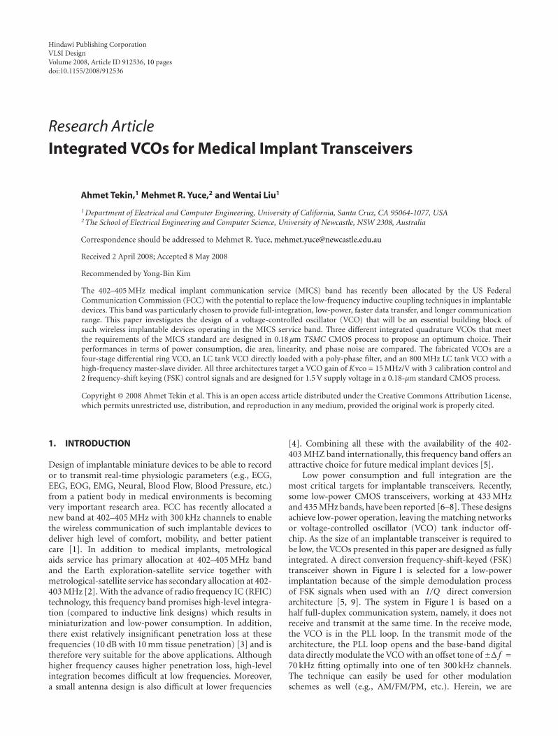
Low power consumption and full integration are themost critical targets for implantable transceivers. Recently,some low-power CMOS transceivers, working at 433 MHzand 435 MHz bands, have been reported [6–8]. These designsachieve low-power operation, leaving the matching networksor voltage-controlled oscillator (VCO) tank inductor off-chip. As the size of an implantable transceiver is required tobe low, the VCOs presented in this paper are designed as fullyintegrated. A direct conversion frequency-shift-keyed (FSK)transceiver shown in Figure 1 is selected for a low-powerimplantation because of the simple demodulation processof FSK signals when used with an I/Q direct conversionarchitecture [5, 9]. The system in Figure 1 is based on ahalf full-duplex communication system, namely, it does notreceive and transmit at the same time. In the receive mode,the VCO is in the PLL loop. In the transmit mode of thearchitecture, the PLL loop opens and the base-band digitaldata directly modulate the VCO with an offset tone of±Δ f =70 kHz fitting optimally into one of ten 300 kHz channels.The technique can easily be used for other modulationschemes as well (e.g., AM/FM/PM, etc.). Herein, we are
2 VLSI Design
RFswitch
LNA
X
Mixers FilterI
Limiter amplifier
xI
Data
Demod.
Clock
xQ
QX
TX
ctr
RX
ctr PA
PA: Power amplifier
Buff I QBuffers
PLLDatain
Figure 1: Block diagram of an MICS transceiver. The shadow area shows the transmitter part.
Vref.high
Comparators Combinationallogic
Vref.low
up
dw
Up/downcounter
(I,Q) to PAand mixers
VCO
128/129 (I,Q)
M
PFD
Fref
up
dwCP
Vctr
DatainRX/TX
LF
(a)
VCO’s powerspectrum
300 kHz
20
Adjacentchannel
70 80
150 kHz
0
(b)
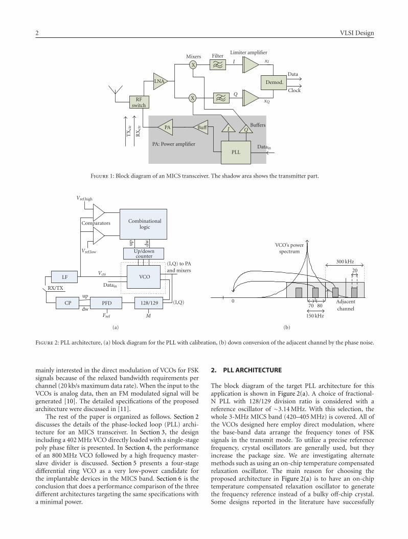
Figure 2: PLL architecture, (a) block diagram for the PLL with calibration, (b) down conversion of the adjacent channel by the phase noise.
mainly interested in the direct modulation of VCOs for FSKsignals because of the relaxed bandwidth requirements perchannel (20 kb/s maximum data rate). When the input to theVCOs is analog data, then an FM modulated signal will begenerated [10]. The detailed specifications of the proposedarchitecture were discussed in [11].
The rest of the paper is organized as follows. Section 2discusses the details of the phase-locked loop (PLL) archi-tecture for an MICS transceiver. In Section 3, the designincluding a 402 MHz VCO directly loaded with a single-stagepoly phase filter is presented. In Section 4, the performanceof an 800 MHz VCO followed by a high frequency master-slave divider is discussed. Section 5 presents a four-stagedifferential ring VCO as a very low-power candidate forthe implantable devices in the MICS band. Section 6 is theconclusion that does a performance comparison of the threedifferent architectures targeting the same specifications witha minimal power.
2. PLL ARCHITECTURE
The block diagram of the target PLL architecture for thisapplication is shown in Figure 2(a). A choice of fractional-N PLL with 128/129 division ratio is considered with areference oscillator of ∼3.14 MHz. With this selection, thewhole 3-MHz MICS band (420–405 MHz) is covered. All ofthe VCOs designed here employ direct modulation, wherethe base-band data arrange the frequency tones of FSKsignals in the transmit mode. To utilize a precise referencefrequency, crystal oscillators are generally used, but theyincrease the package size. We are investigating alternatemethods such as using an on-chip temperature compensatedrelaxation oscillator. The main reason for choosing theproposed architecture in Figure 2(a) is to have an on-chiptemperature compensated relaxation oscillator to generatethe frequency reference instead of a bulky off-chip crystal.Some designs reported in the literature have successfully
Ahmet Tekin et al. 3
GM
RP
RC RL
C L
+
−
(a)
M6
Iref
Cal0 Cal1 Cal2 FSK0 FSK1
M5
M4 M3
2L
D1 D2M1 M2
Vctr
Cbp
LO+
LO−Cbp
Cal0 Cal1 Cal2 FSK0 FSK1
Rfil
Cfil
Rfil
Cfil
Rfil
Cfil
Rfil
Cfil
Q−
I+
Q+
I−
Rbias
Vbias
To the mixersand PA
(b)
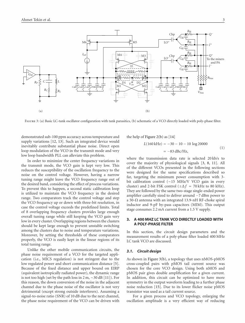
Figure 3: (a) Basic LC-tank oscillator configuration with tank parasitics, (b) schematic of a VCO directly loaded with poly-phase filter.
demonstrated sub-100 ppm accuracy across temperature andsupply variations [12, 13]. Such an integrated device wouldinevitably contribute substantial phase noise. Direct openloop modulation of the VCO in the transmit mode and verylow loop bandwidth PLL can alleviate this problem.
In order to minimize the center frequency variations inthe transmit mode, the VCO gain is kept very low. Thisreduces the susceptibility of the oscillation frequency to thenoise on the control voltage. However, having a narrowtuning range might leave the VCO frequency range out ofthe desired band, considering the effect of process variations.To prevent this to happen, a second static calibration loopis utilized to maintain the VCO frequency in the desiredrange. Two comparators track the control voltage and stepthe VCO frequency up or down with three-bit resolution, incase the control voltage exceeds the predefined limits. Totalof 8 overlapping frequency clusters provides large enoughoverall tuning range while still keeping the VCO gain verylow in every cluster. Overlapping regions between the clustersshould be kept large enough to prevent unstable switchingamong the clusters due to noise and temperature variations.Moreover, by setting the thresholds of these comparatorsproperly, the VCO is easily kept in the linear regions of itstotal tuning range.
Unlike the other mobile communication circuits, thephase noise requirement of a VCO for the targeted appli-cation (i.e., MICS regulation) is not stringent due to thelow regulated power and short communication distance [5].Because of the fixed distance and upper bound on EIRP(equivalent isotropically radiated power), the dynamic rangeis not too high (set by the path loss in 2 m, ∼30 dB [11]). Forthis reason, the down conversion of the noise in the adjacentchannel due to the phase noise of the oscillator is not verydetrimental (except strong outside interferers). Assuming asignal-to-noise ratio (SNR) of 10 dB due to the next channel,the phase noise requirement of the VCO can be driven with
the help of Figure 2(b) as [14]
L(160 kHz) = −30− 10− 10 log 20000
= −83 dBc/Hz,(1)
where the transmission data rate is selected 20 kb/s tocover the majority of physiological signals [3, 8, 11]. Allof the different VCOs presented in the following sectionswere designed for the same specifications described sofar, targeting the minimum power consumption with 3-bit calibration control (∼15 MHz/V VCO gain in everycluster) and 2-bit FSK control (±Δ f = 70 kHz to 80 kHz).They are followed by the same two-stage single-ended poweramplifier carefully sized to deliver around −7 dBm power toa 50-Ω antenna with an integrated 13.9-nH RF-choke spiralinductor and 9-pF by-pass capacitors (MIM). This outputstage consumes 2.2 mA current from a 1.5 V supply.
3. A 400 MHZ LC TANK VCO DIRECTLY LOADED WITHA POLY-PHASE FILTER
In this section, the circuit design parameters and themeasurement results of a poly-phase filter loaded 400 MHzLC tank VCO are discussed.
3.1. Circuit design
As shown in Figure 3(b), a topology that uses nMOS-pMOScross-coupled pairs with pMOS tail current source waschosen for the core VCO design. Using both nMOS andpMOS pair gives double amplification for a given current.In addition, this circuit can be optimized to have moresymmetry in the output waveform leading to a further phasenoise reduction [15]. Due to its lower flicker noise pMOStransistor was used as a tail current source.
For a given process and VCO topology, enlarging theoscillation amplitude is a very efficient way of reducing
4 VLSI Design
the phase noise [16]. For a given current level, this canbe achieved by maximizing the values of the resonant tankinductors [17]. However, there are some serious limitationson the value of the inductor if the inductor is to be integratedin a CMOS process. As the value of the inductance in aspiral inductor increases, the resistive losses associated withit would degrade the Q of this inductor, which is the mostimportant phase noise source in a fully integrated VCO.Thus, it is desirable to construct large inductors with verylow resistive losses [16]. An 8-turn 22.4 nH spiral inductorwith a trace width of w = 12 μm and gap of s = 1.5 μmis used for this design. Only the top metal layer (metal6)was used for the spirals which would result in a total seriesresistance of Rind = 20Ω at 400 MHz. The quality factor ofthis inductor at 400 MHz is 5.2. The total tank capacitancecorresponding to this inductance value is Ctot = 7.07 pF.This total capacitance represents all the parasitic capacitancesassociated with the FETs, capacitive loading due to poly-phase filter, 3-bit binary weighted MIM-Caps for calibration,and varactor diodes for tuning. Moreover, two switchable 7-fF metal2-metal3 capacitors were used for FSK modulation.
The basic configuration for an LC tank oscillator is givenin Figure 3(a) [16]. To satisfy the oscillation condition, thetransconductance necessary to have the unity loop gain at theoscillation frequency, ωo , can be calculated from the transferfunction as [16]
GM = Reff
(ωoC
)2, (2)
where Reff = RC + RL + 1/(RP(ωoC)2). RP is the paralleltank resistance, RL is the inductor series resistance, and RC
is the varactor series resistance. The most important term indetermining the value of Reff is the series resistance of theinductor at 400 MHz, which is approximately 20Ω. Using(1), the transconductance required to compensate the lossescan be calculated as
GM = 20Ω · (2π · 0.4 GHz · 7.07 pF)2 = 6.5 mS. (3)
Therefore, each transistor should have a gm of 6.5 mS.Thus, with a safety factor of 3, the design assumes 20-mS transconductance for each device. Current required toachieve the given transconductance value with an over-drivevoltage of VGS − VT = 0.12 V would be ID = gm(VGS −VT)/2 ∼= 1 mA.Hence, the total tail current of VCO core is setto be 2 mA from a 1.5-V supply during the simulations. Thecorresponding transistor W/L ratios are 100 μm/0.18 μm fornMOS pair transistors and three times bigger for the pMOSpair devices.
Using a poly-phase filter to generate quadrature phasesis a popular approach for low power, I-Q mismatch tolerantapplications [18, 19]. In general, these filters have low inputimpedance and require power hungry buffers to drive themafter the VCO. They might also require buffers followingthem to drive the mixers (Figure 1). These buffers isolate themixer input capacitance from the filter and also provide thesignal swing required for the mixer.
For this specific application, taking advantage of rel-atively low operating frequency, both buffers have been
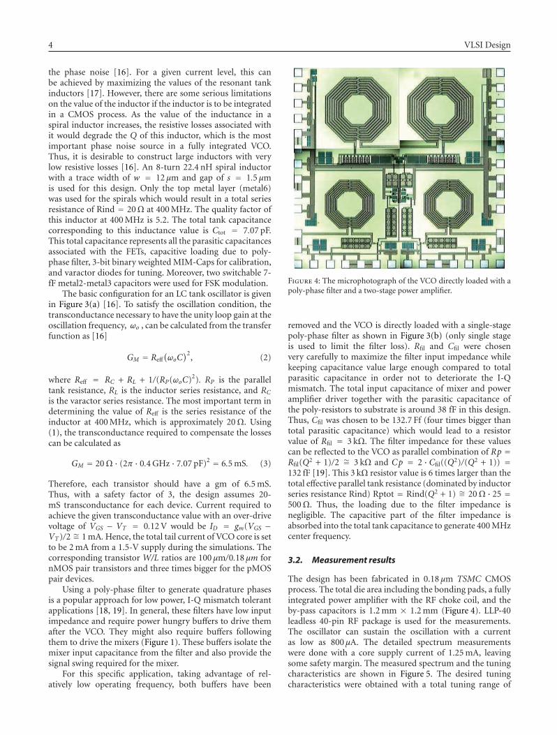
Figure 4: The microphotograph of the VCO directly loaded with apoly-phase filter and a two-stage power amplifier.
removed and the VCO is directly loaded with a single-stagepoly-phase filter as shown in Figure 3(b) (only single stageis used to limit the filter loss). Rfil and Cfil were chosenvery carefully to maximize the filter input impedance whilekeeping capacitance value large enough compared to totalparasitic capacitance in order not to deteriorate the I-Qmismatch. The total input capacitance of mixer and poweramplifier driver together with the parasitic capacitance ofthe poly-resistors to substrate is around 38 fF in this design.Thus, Cfil was chosen to be 132.7 Ff (four times bigger thantotal parasitic capacitance) which would lead to a resistorvalue of Rfil = 3 kΩ. The filter impedance for these valuescan be reflected to the VCO as parallel combination of Rp =Rfil(Q2 + 1)/2 ∼= 3 kΩ and Cp = 2 ·Cfil((Q2)/(Q2 + 1)) =132 fF [19]. This 3 kΩ resistor value is 6 times larger than thetotal effective parallel tank resistance (dominated by inductorseries resistance Rind) Rptot = Rind(Q2 + 1) ∼= 20Ω · 25 =500Ω. Thus, the loading due to the filter impedance isnegligible. The capacitive part of the filter impedance isabsorbed into the total tank capacitance to generate 400 MHzcenter frequency.
3.2. Measurement results
The design has been fabricated in 0.18 μm TSMC CMOSprocess. The total die area including the bonding pads, a fullyintegrated power amplifier with the RF choke coil, and theby-pass capacitors is 1.2 mm × 1.2 mm (Figure 4). LLP-40leadless 40-pin RF package is used for the measurements.The oscillator can sustain the oscillation with a currentas low as 800 μA. The detailed spectrum measurementswere done with a core supply current of 1.25 mA, leavingsome safety margin. The measured spectrum and the tuningcharacteristics are shown in Figure 5. The desired tuningcharacteristics were obtained with a total tuning range of

Ahmet Tekin et al. 5
0
−20
−40
−60
−80
−100
−120
Pow
er(d
Bm
)
4.08 4.1 4.12 4.14 4.16 4.18 4.2
×108Frequency (Hz)
(a)
480
460
440
420
400
380
360
340
Freq
uen
cy(M
Hz)
0 0.3 0.5 0.8 1 1.3 1.5
Vctr (V)
Vlow
Vhigh
MICSregion
(b)
Figure 5: (a) The measured spectrum of the VCO with poly-phase filter, (b) the measured tuning characteristics of this VCO.
−40
−60
−80
−100
−120
−140
Ph
ase
noi
se(d
Bc/
Hz)
103 104 105 106 107
Frequency offset (Hz)
(a)
−95
−100
−105
−110
−115
Ph
ase
noi
se(d
Bc/
Hz)
0.8 1 1.2 1.4 1.6 1.8
Total current (mA)
At 300 kHz offsetAt 160 kHz offset
(b)
Figure 6: (a) The measured phase noise of the VCO with poly-phase filter, (b) phase noise for various VCO core current levels.
90 MHz spread into 3-bit controlled 8 clusters. The VCOgain inside every cluster is around 15 MHz/V as expected.Although the most significant bit (MSB) of the calibrationinput causes a larger step in the tuning range, a safe overlapcan still be observed. The FSK control bits caused 60-kHz tones around the center frequency. Although this tonefrequency still can be employed with FSK, this value caneasily be tuned to the desired 70-kHz tone in the nextiteration of the design by modifying the FSK capacitors. Thephase noise measurement is done with Agilent E5052A. Thephase noise at an offset of 160 kHz is −98 dBc/Hz, whichis far below the prerequisite value for the application. Thephase noise plot is shown in Figure 6(a). Figure 6(b) showsthe phase noise values at the offsets of interest for variouspower levels.
4. AN 800 MHZ LC TANK VCO WITHA MASTER-SLAVE DIVIDER
Another way to generate quadrature signals is to use amaster-slave divide-by-2 circuit following a VCO operatingat double frequency. In this section, the performance of an800 MHz LC tank VCO with an analog master-slave divideris discussed. The divider outputs drive the same mixer andpower amplifier load as in the case of first design (as shownin Figure 1).
4.1. Circuit design
Since the fast analog D-flip-flops of the divider circuit needsto be driven with high swing inputs, a VCO topology withonly nMOS cross-coupled pair is used to have a higher swing

6 VLSI Design
(a) (b)
M4 M3
IbL L
Cal0 Cal1 Cal2 FSK0 FSK1
M1 M2
VctrCal0 Cal1 Cal2 FSK0 FSK1
VCO+
VCO−
D+
D−
C+ C− C+ C−Q+
Q−D+
D−Q+
Q−S-DFFM-DFF
QI
M1 M2 M3 M4
M5M6
M7 M8
M9 M10
M11
Vbp
D+
C+
Q+
D−
Q−
C−
Vbn
Figure 7: The schematic for 800 MHz VCO with master-slave divider.
at the oscillator output. The circuit schematic of the designincluding the divider is shown in Figure 7. Two 13.69-nHspiral inductors with 7 turns are used for this 800-MHzLC tank. The top metal (metal6) with conductor widthw = 9 μm and conductor spacing s = 1.5 μm yields aneffective series resistance of 13Ω. Q factor for this inductor isaround 4.2 at the frequency of 800 MHz. The total of 2.89 pFtank capacitance includes varactor diode capacitances, 3-bitbinary weighted switchable MIM-caps, parasitic gate-source,and drain-source capacitances of the cross coupled nMOSpair and the parasitic input gate capacitance of the dividercircuit. Two 5-fF metal2-meatl3 capacitances are used fordirect FSK modulation by the base-band binary data. Thetotal effective series resistance of the tank was estimated to be16Ω with an additional up to 3-Ω varactor series resistance.Again using (2), the overall required transconductance iscalculated to be 3.36 mS. Assuming a safety factor of 3, eachnMOS device of the cross-coupled pair should have a gm ofaround 20 mS to sustain reliable oscillation. This transcon-ductance value can be obtained by having 1 mA currentthrough each branch with 120 mV overdrive voltage across100 μm width minimum channel length nMOS devices. Acurrent source pMOS device of 400 μm channel width and0.3 μm channel length can support this 2-mA total currentwith an overdrive voltage of 140 mV.
A very common topology shown in Figure 7 was usedfor fast divide-by-2 operation. In this design, M3 and M4would not allow a large voltage drop at the drains of M1 andM2, which otherwise would push M11 into triode region incase of a large VCO output driving this stage, particularly inthe case of a low supply voltage. Transistors were carefullysized to achieve successful division using a 1.5-V supply
Differentialring VCO
RingVCO PA Output
PA
800 MHzLC VCO Divide
Figure 8: The microphotograph of the chip including an 800 MHzLC tank VCO with dividers and a four-stage differential ring VCO.
with minimum power consumption. The divider circuit candirectly drive the mixers and the PA consuming 400 μA froma 1.5-V supply [20].
4.2. Measurement results
The design has been fabricated in 0.18 μm TSMC CMOSprocess. The total die area including the bonding pads, a fullyintegrated power amplifier with the RF choke coil and theby-pass capacitors is 1.1 mm × 1.2 mm (Figure 8). The VCO
Ahmet Tekin et al. 7
440
430
420
410
400
390
380
370
Freq
uen
cy(M
Hz)
0 0.5 1 1.5
Vctr (V)
Vth-low
Thresholds forcomparator Vth-high
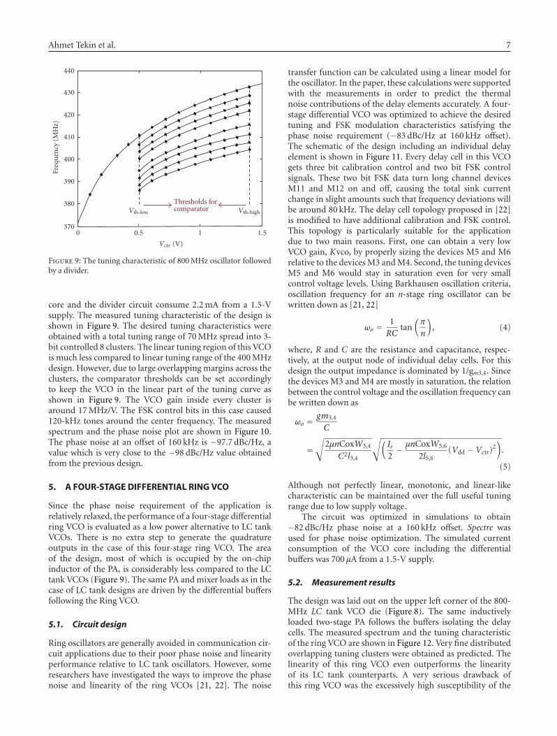
Figure 9: The tuning characteristic of 800 MHz oscillator followedby a divider.
core and the divider circuit consume 2.2 mA from a 1.5-Vsupply. The measured tuning characteristic of the design isshown in Figure 9. The desired tuning characteristics wereobtained with a total tuning range of 70 MHz spread into 3-bit controlled 8 clusters. The linear tuning region of this VCOis much less compared to linear tuning range of the 400 MHzdesign. However, due to large overlapping margins across theclusters, the comparator thresholds can be set accordinglyto keep the VCO in the linear part of the tuning curve asshown in Figure 9. The VCO gain inside every cluster isaround 17 MHz/V. The FSK control bits in this case caused120-kHz tones around the center frequency. The measuredspectrum and the phase noise plot are shown in Figure 10.The phase noise at an offset of 160 kHz is −97.7 dBc/Hz, avalue which is very close to the −98 dBc/Hz value obtainedfrom the previous design.
5. A FOUR-STAGE DIFFERENTIAL RING VCO
Since the phase noise requirement of the application isrelatively relaxed, the performance of a four-stage differentialring VCO is evaluated as a low power alternative to LC tankVCOs. There is no extra step to generate the quadratureoutputs in the case of this four-stage ring VCO. The areaof the design, most of which is occupied by the on-chipinductor of the PA, is considerably less compared to the LCtank VCOs (Figure 9). The same PA and mixer loads as in thecase of LC tank designs are driven by the differential buffersfollowing the Ring VCO.
5.1. Circuit design
Ring oscillators are generally avoided in communication cir-cuit applications due to their poor phase noise and linearityperformance relative to LC tank oscillators. However, someresearchers have investigated the ways to improve the phasenoise and linearity of the ring VCOs [21, 22]. The noise
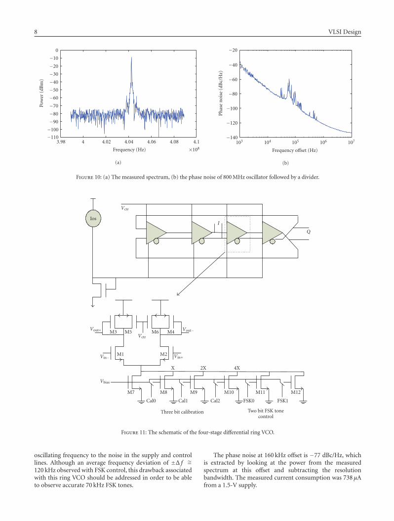
transfer function can be calculated using a linear model forthe oscillator. In the paper, these calculations were supportedwith the measurements in order to predict the thermalnoise contributions of the delay elements accurately. A four-stage differential VCO was optimized to achieve the desiredtuning and FSK modulation characteristics satisfying thephase noise requirement (−83 dBc/Hz at 160 kHz offset).The schematic of the design including an individual delayelement is shown in Figure 11. Every delay cell in this VCOgets three bit calibration control and two bit FSK controlsignals. These two bit FSK data turn long channel devicesM11 and M12 on and off, causing the total sink currentchange in slight amounts such that frequency deviations willbe around 80 kHz. The delay cell topology proposed in [22]is modified to have additional calibration and FSK control.This topology is particularly suitable for the applicationdue to two main reasons. First, one can obtain a very lowVCO gain, Kvco, by properly sizing the devices M5 and M6relative to the devices M3 and M4. Second, the tuning devicesM5 and M6 would stay in saturation even for very smallcontrol voltage levels. Using Barkhausen oscillation criteria,oscillation frequency for an n-stage ring oscillator can bewritten down as [21, 22]
ωo = 1RC
tan(π
n
), (4)
where, R and C are the resistance and capacitance, respec-tively, at the output node of individual delay cells. For thisdesign the output impedance is dominated by 1/gm3,4. Sincethe devices M3 and M4 are mostly in saturation, the relationbetween the control voltage and the oscillation frequency canbe written down as
ωo =gm3,4
C
=√
2μnCoxW3,4
C2l3,4
√(Is2− μnCoxW5,6
2l5,6(Vdd −Vctr)
2).
(5)
Although not perfectly linear, monotonic, and linear-likecharacteristic can be maintained over the full useful tuningrange due to low supply voltage.
The circuit was optimized in simulations to obtain−82 dBc/Hz phase noise at a 160 kHz offset. Spectre wasused for phase noise optimization. The simulated currentconsumption of the VCO core including the differentialbuffers was 700 μA from a 1.5-V supply.
5.2. Measurement results
The design was laid out on the upper left corner of the 800-MHz LC tank VCO die (Figure 8). The same inductivelyloaded two-stage PA follows the buffers isolating the delaycells. The measured spectrum and the tuning characteristicof the ring VCO are shown in Figure 12. Very fine distributedoverlapping tuning clusters were obtained as predicted. Thelinearity of this ring VCO even outperforms the linearityof its LC tank counterparts. A very serious drawback ofthis ring VCO was the excessively high susceptibility of the
8 VLSI Design
0
−10
−20
−30
−40
−50
−60
−70
−80
−90
−100
−110
Pow
er(d
Bm
)
3.98 4 4.02 4.04 4.06 4.08 4.1
×108Frequency (Hz)
(a)
−20
−40
−60
−80
−100
−120
−140
Ph
ase
noi
se(d
Bc/
Hz)
103 104 105 106 107
Frequency offset (Hz)
(b)
Figure 10: (a) The measured spectrum, (b) the phase noise of 800 MHz oscillator followed by a divider.
Ios
Vctr
I
Q
Vout+
Vin−
Vbias
M1 M2
M3 M4M5 M6
M7 M8 M9 M10 M11 M12
Vctr
Vout−
Vin+
Cal0 Cal1 Cal2 FSK0 FSK1
X 2X 4X
Three bit calibration Two bit FSK tonecontrol
Figure 11: The schematic of the four-stage differential ring VCO.
oscillating frequency to the noise in the supply and controllines. Although an average frequency deviation of ±Δ f ∼=120 kHz observed with FSK control, this drawback associatedwith this ring VCO should be addressed in order to be ableto observe accurate 70 kHz FSK tones.
The phase noise at 160 kHz offset is −77 dBc/Hz, whichis extracted by looking at the power from the measuredspectrum at this offset and subtracting the resolutionbandwidth. The measured current consumption was 738 μAfrom a 1.5-V supply.

Ahmet Tekin et al. 9
460
440
420
400
380
360
Freq
uen
cy(M
Hz)
0 0.2 0.4 0.6 0.8 1
Vctr (V)
(a)
0
−20
−40
−60
−80
−100
Pow
er(d
Bm
)
3.85 3.9 3.95 4 4.05
×108Frequency (Hz)
(b)
Figure 12: (a) The tuning characteristic, (b) the measured spectrum of the four-stage differential ring VCO.
Table 1: Comparison table for the three oscillator architectures.
VCO typeCurrentconsumption
Die areaPhase noise @160 kHz offset
LinearityFrequencystability
Supply noisesensitivity
Ring 0.74 mA 0.2 mm × 0.2 mm −77 dBc/Hz Good Poor Sensitive
LC-tank divided 2.20 mA 0.4 mm × 0.7 mm −97 dBc/Hz Moderate Good Immune
LC-tank with PF 1.25 mA 0.6 mm × 0.8 mm −98 dBc/Hz Moderate Good Immune
6. COMPARISON AND CONCLUSION
Three different fully integrated VCOs including the driv-ing buffers and the power amplifiers were designed, andfabricated in 0.18 μm TSMC CMOS process to evaluatethe best option for an MICS band transceiver operating atthe new 402–405 MHz band. Although it consumes verylow power and occupies very small die area, the poorfrequency stability of ring VCO makes it difficult to obtaina reasonable FSK tone for 300 kHz channel spacing in MICSband. Moreover, the measured phase noise was 5 dB morethan the predefined maximum level. The 800 MHz LCtank VCO with master-slave divider achieves almost thesame phase noise performance at the expense of almostdouble power consumption, compared to the 400 MHzLC tank VCO directly loaded with poly-phase filter. Thelinearity of the tuning curve of 800 MHz design is worsethan the 400 MHz one. The measurement results of thesethree architectures were summarized in a comparison table(Table 1). In conclusion, a carefully designed 400 MHz LCtank driving a poly-phase filter was proven to be the bestoption for this application.
ACKNOWLEDGMENTS
The authors would like to thank Masood Yousefi, AliKiaei, Bijoy G Chatterjee, Ahmad Bahai, Raj Subramoniam,and Virginia Abellera of National Semiconductor for theirsupport and collaboration in the project. M. Yuce’s work
is supported by the Australian ARC discovery Grant no.DP0772929.
REFERENCES
[1] FCC Rules and Regulations, “MICS Band Plan,” Table ofFrequency Allocations, Part 95, January 2003.
[2] Australian Communications Authority, Radio FrequencyPlanning Group, “Planning for Medical Implant Communi-cations Systems & Related Devices,” Proposals Paper, October2003, http://www.acma.gov.au.
[3] W. G. Scanlon, J. B. Burns, and N. E. Evans, “Radiowavepropagation from a tissue-implanted source at 418 MHz and916.5 MHz,” IEEE Transactions on Biomedical Engineering, vol.47, no. 4, pp. 527–534, 2000.
[4] A. K. Skrivervik, J.-F. Zurcher, O. Staub, and J. R. Mosig,“PCS antenna design: the challenge of miniaturization,” IEEEAntennas and Propagation Magazine, vol. 43, no. 4, pp. 12–27,2001.
[5] P. Bradley, “An ultra low power, high performance medi-cal implant communication system (MICS) transceiver forimplantable devices,” in Proceedings of the IEEE BiomedicalCircuits and Systems Conference (BioCAS ’06), London, UK,November -December, 2006.
[6] T. Melly, A.-S. Porret, C. C. Enz, and E. A. Vittoz, “An ultralow-power UHF transceiver integrated in a standard digital CMOSprocess: transmitter,” IEEE Journal of Solid-State Circuits, vol.36, no. 3, pp. 467–472, 2001.
[7] E. Zencir, T.-H. Huang, A. Tekin, N. S. Dogan, and E. Arvas,“UHF RF front-end circuits in 0.35-μm silicon on insulator

10 VLSI Design
(SOI) CMOS,” Analog Integrated Circuits and Signal Processing,vol. 45, no. 3, pp. 231–245, 2005.
[8] N. M. Neihart and R. R. Harrison, “Micropower circuits forbidirectional wireless telemetry in neural recording applica-tions,” IEEE Transactions on Biomedical Engineering, vol. 52,no. 11, pp. 1950–1959, 2005.
[9] A.-S. Porret, T. Melly, D. Python, C. C. Enz, and E. A. Vittoz,“An ultralow-power UHF transceiver integrated in a standarddigital CMOS process: architecture and receiver,” IEEE Journalof Solid-State Circuits, vol. 36, no. 3, pp. 452–466, 2001.
[10] Y. B. Choi, T. H. Teo, and W. G. Yeoh, “A 2.4 GHz fullyintegrated CMOS VCO with direct FM/FSK modulationcapability,” in Proceedings of the IEEE Conference on ElectronDevices and Solid-State Circuits (EDSSC ’03), pp. 175–178,Hong Kong, December 2003.
[11] A. Tekin, M. R. Yuce, and W. Liu, “A low power MICS bandtransceiver architecture for implantable devices,” in Proceed-ings of the IEEE Annual Conference on Wireless and MicrowaveTechnology (WAMICON ’05), pp. 55–58, Clearwater, Fla, USA,April 2005.
[12] J. B. Nolan and R. S. Ellison, “Calibration techniques for a pre-cision relaxation oscillator integrated circuit with temperaturecompensation,” US patent 299338, March 2002.
[13] M. H. Splithof, A. J. M. van Tuijl, S. L. J. Gierkink, and E.A. M. Klumperink, “Current-ratio temperature compensationin bipolar relaxation oscillator,” in Proceedings of the 24thEuropean Solid-State Circuits Conference (ESSCIRC ’98), pp.392–395, The Hague, The Netherlands, September 1998.
[14] B. Razavi, RF Microelectronics, Prentice-Hall, Upper SaddleRiver, NJ, USA, 1998.
[15] J. Bhattacharjee, D. Mukherjee, E. Gebara, S. Nuttinck, and J.Laskar, “A 5.8 GHz fully integrated low power low phase noiseCMOS LC VCO for WLAN applications,” in Proceedings of theIEEE MTT-S International Microwave Symposium Digest, vol.1, pp. 585–588, Seattle, Wash, USA, June 2002.
[16] J. Craninckx and M. Steyaert, Wireless CMOS FrequencySynthesizer Design, Kluwer Academic Publishers, Dordrecht,The Netherlands, 1998.
[17] B. Razavi, “A 1.8 GHz CMOS voltage-controlled oscillator,” inProceedings of the 43rd IEEE International Solid-State CircuitsConference (ISSCC ’97), pp. 388–389, San Francisco, Calif,USA, February 1997.
[18] M. Borremans, M. Steyaert, and T. Yoshitomi, “A 1.5 V, wideband 3 GHz, CMOS quadrature direct up-converter for multi-mode wireless communications,” in Proceedings of the IEEECustom Integrated Circuits Conference, pp. 79–82, Santa Clara,Calif, USA, May 1998.
[19] M. Borremans, B. De Muer, and M. Steyaert, “The optimiza-tion of GHz integrated CMOS quadrature VCO’s based on apoly-phase filter loaded differential oscillator,” in Proceedingsof the IEEE International Symposium on Circuits and Systems(ISCAS ’00), vol. 2, pp. 729–732, Geneva, Switzerland, May2000.
[20] J. F. Parker and D. Ray, “A 1.6-GHz CMOS PLL with on-chiploop filter,” IEEE Journal of Solid-State Circuits, vol. 33, no. 3,pp. 337–343, 1998.
[21] B. Razavi, “A study of phase noise in CMOS oscillators,” IEEEJournal of Solid-State Circuits, vol. 31, no. 3, pp. 331–343, 1996.
[22] H. Chen and R. Geiger, “Transfer characterization of CMOSring voltage controlled oscillators,” in Proceedings of the 44thIEEE Midwest Symposium on Circuits and Systems (MWS-CAS ’01), vol. 1, pp. 66–70, Dayton, Ohio, USA, August 2001.