instrumentation & measurements mech 430 chapter 7 sampling
TRANSCRIPT

- +
Instrumentation & Measurements MECH 430
MECH 430 Slide 1
Chapter 7 Sampling, Digital Devices, and Data
Acquisition

- +
Data Acquisition • Integrating analog electrical transducers with digital
devices is cost effective and common-place. • Digital microprocessors are central to most
controllers and data-acquisitions systems today. • How can an analog signal be represented in digital
form and what are the drawbacks? • We will discuss Analog to Digital (A2D) and Digital
to Analog (D2A) devices.
MECH 430 Introduction Slide 2
- +
MECH 430 SC_A/D conversion Slide 3
Analog to Digital Conversion
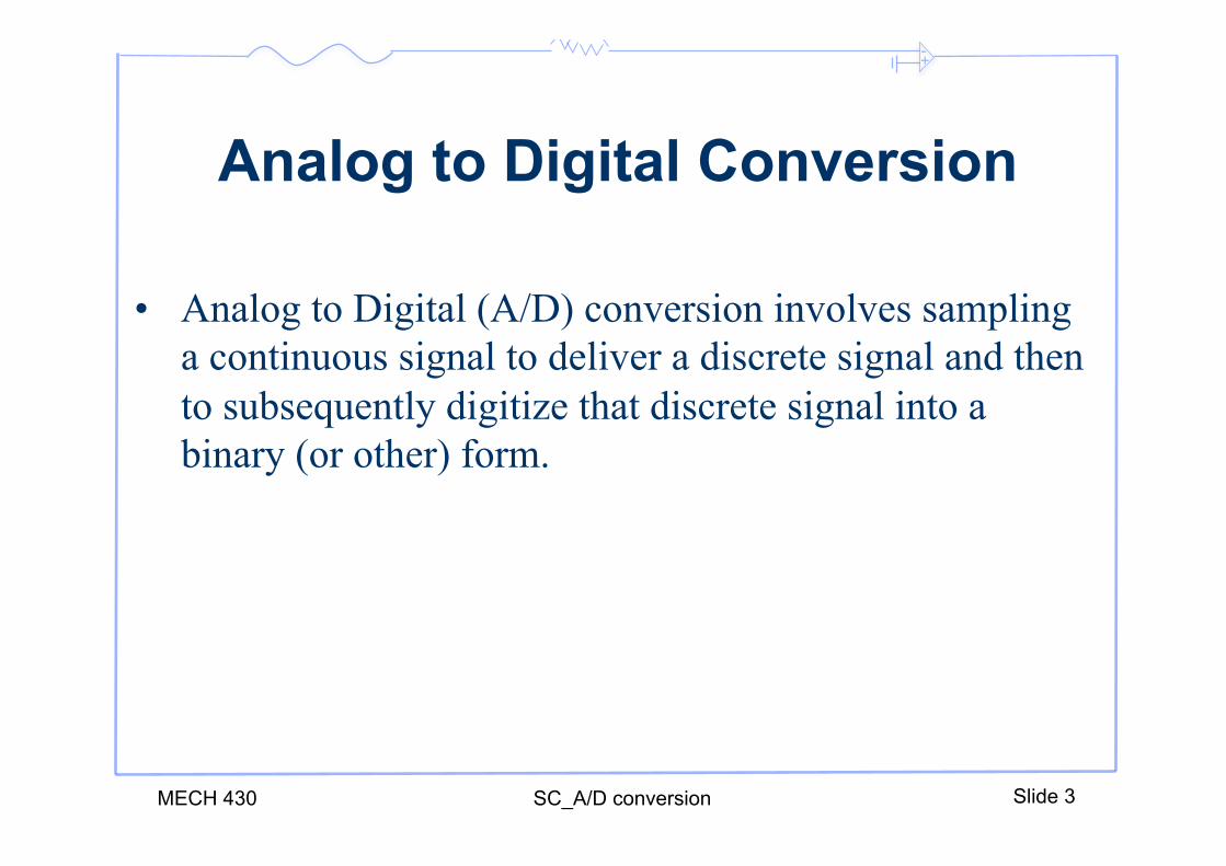
• Analog to Digital (A/D) conversion involves sampling a continuous signal to deliver a discrete signal and then to subsequently digitize that discrete signal into a binary (or other) form.

- +
MECH 430 SC_A/D conversion Slide 4
Analog to Digital Conversion
Measurand
Sensor & signal
conditioning
Physical signal Temperature
Pressure Displacement
Flow,…
Electrical signal Voltage Current
Electrical signal conversion
1)Sampling (fs > 2fin_high) to avoid aliasing 2) Digitization
Tin
inin Tf 1=
ss Tf 1=
Ts
A/D Converter
xV
1 2 3
N
Computer
Digital signal
00101001)4(00101001)3(00011001)2(00001001)1(
=
=
=
=
VVVV
N
- +
MECH 430 SC_A/D conversion Slide 5
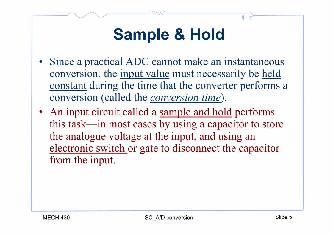
Sample & Hold • Since a practical ADC cannot make an instantaneous
conversion, the input value must necessarily be held constant during the time that the converter performs a conversion (called the conversion time).
• An input circuit called a sample and hold performs this task—in most cases by using a capacitor to store the analogue voltage at the input, and using an electronic switch or gate to disconnect the capacitor from the input.

- +
MECH 430 SC_A/D conversion Slide 6
Sample & Hold + - vi
vo C
• The closure time τ of the switch is relatively short and the samples obtained are stored on the capacitor.
• Each of these voltages is then fed to the input of the ADC, which provides an N-bit binary number proportional to the value of signal sample.
- +
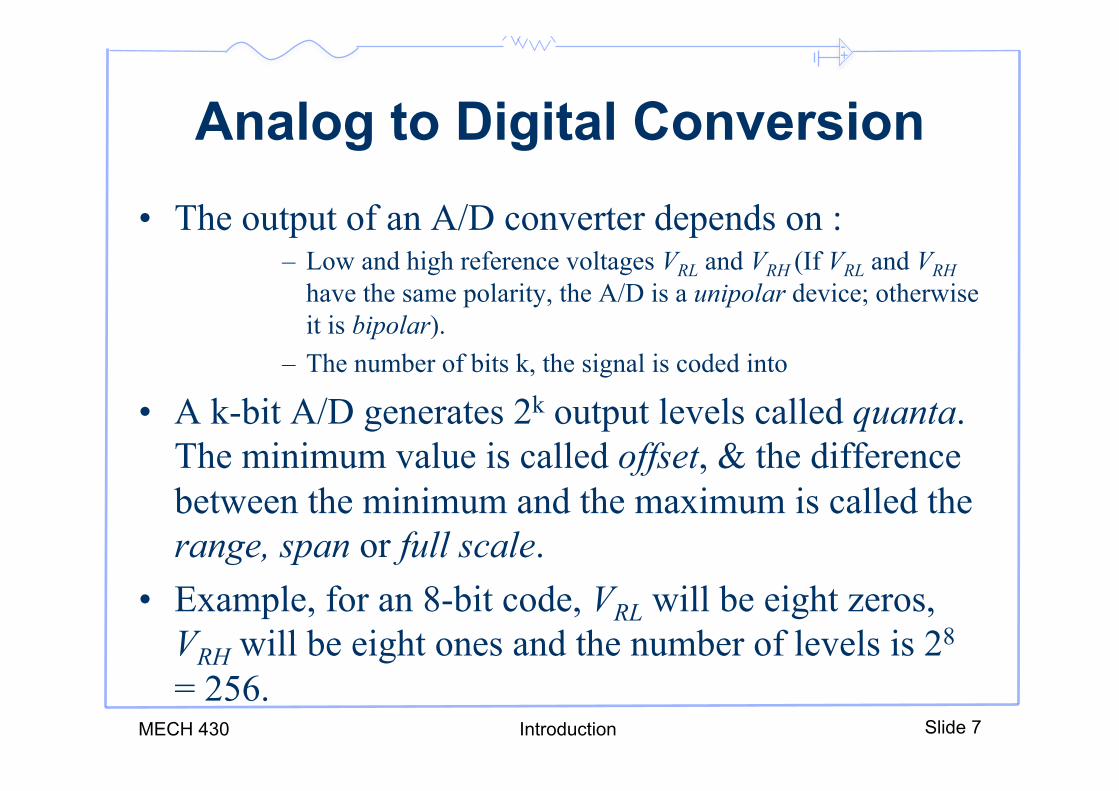
Analog to Digital Conversion • The output of an A/D converter depends on :
– Low and high reference voltages VRL and VRH (If VRL and VRH have the same polarity, the A/D is a unipolar device; otherwise it is bipolar).
– The number of bits k, the signal is coded into
• A k-bit A/D generates 2k output levels called quanta. The minimum value is called offset, & the difference between the minimum and the maximum is called the range, span or full scale.
• Example, for an 8-bit code, VRL will be eight zeros, VRH will be eight ones and the number of levels is 28 = 256.
MECH 430 Introduction Slide 7
- +
MECH 430 SC_A/D conversion Slide 8
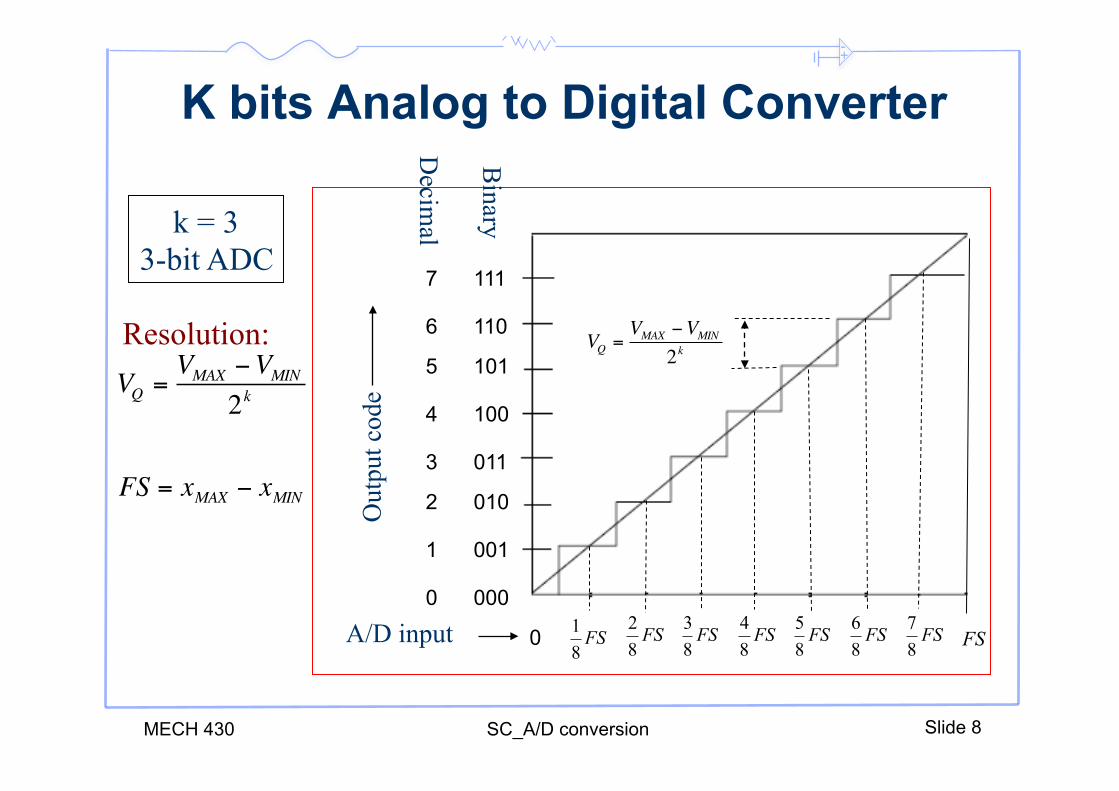
K bits Analog to Digital Converter
FSFS81 FS
84FS
82 FS
83 FS
86FS
85 FS
87
Binary k = 3
3-bit ADC
Out
put c
ode
VQ =VMAX −VMIN
2k
VQ =VMAX −VMIN
2k
FS = xMAX − xMIN
000 0
001 1
010 2
011 3
100 4
101 5
110 6
111 7
A/D input 0
Resolution:
Decim
al

- +
MECH 430 SC_A/D conversion Slide 9
Resolution • The resolution of the converter indicates the number of
discrete values it can produce over the range of voltage values. It is the smallest variation in the analog input signal that would cause the A/D output code to change by one level or quantum.
• It is usually expressed in bits. For example, an ADC that encodes an analog input to one of 256 discrete values (0..255) has a resolution of 8 bits since
• Resolution can also be defined electrically, and expressed in volts. The voltage resolution of an ADC is equal to its overall voltage measurement range (FS) divided by the number of discrete values:
25628 =
VQ =VMAX −VMIN
2k

- +
MECH 430 SC_A/D conversion Slide 10
Resolution Example 1: Full scale measurement range = 0 to 10 volts If ADC resolution is 12 bits: 212 = 4096 quantization levels ADC voltage resolution is: (10-0)/(4096) = 0.00244 volts = 2.44 mV Example 2: Full scale measurement range = -10 to +10 volts If ADC resolution is 14 bits: 214 = 16384 quantization levels ADC voltage resolution is: (10-(-10))/(16384) = 20/16383 = 0.00122 volts = 1.22 mV

- +
MECH 430 SC_A/D conversion Slide 11
Resolution
• In practice, the resolution of the converter is limited by the signal-to-noise (SNR) ratio of the signal in question.
• If there is too much noise present in the analog input, it will be impossible to accurately resolve beyond a certain number of bits of resolution, the “Effective Number Of Bits" (ENOB).
• While the ADC will produce a result, the result is not accurate, since its lower bits are simply measuring noise.

- +
Input-Output Mapping
• Any input voltage vi is translated to its decimal equivalent N as:
MECH 430 Introduction Slide 12
N = INT 2k
FS× vi −VRL[ ]#
$%&
'(
• Going the other way around, to find an analog voltage corresponding to a specific output N we use:
vi = N ×FS2k
"#$
%&'+VRL
FS = xMAX − xMIN
(1)
We will see what this is shortly

- +
MECH 430 SC_A/D conversion Slide 13
A/D Conversion Relations
• Equation (1) can be stated as:
• The decimal equivalent to a binary output N = bn…b1b0
bi is its bit value wi is its weight
• For example if N = 10110010:
- +
MECH 430 SC_A/D conversion Slide 14
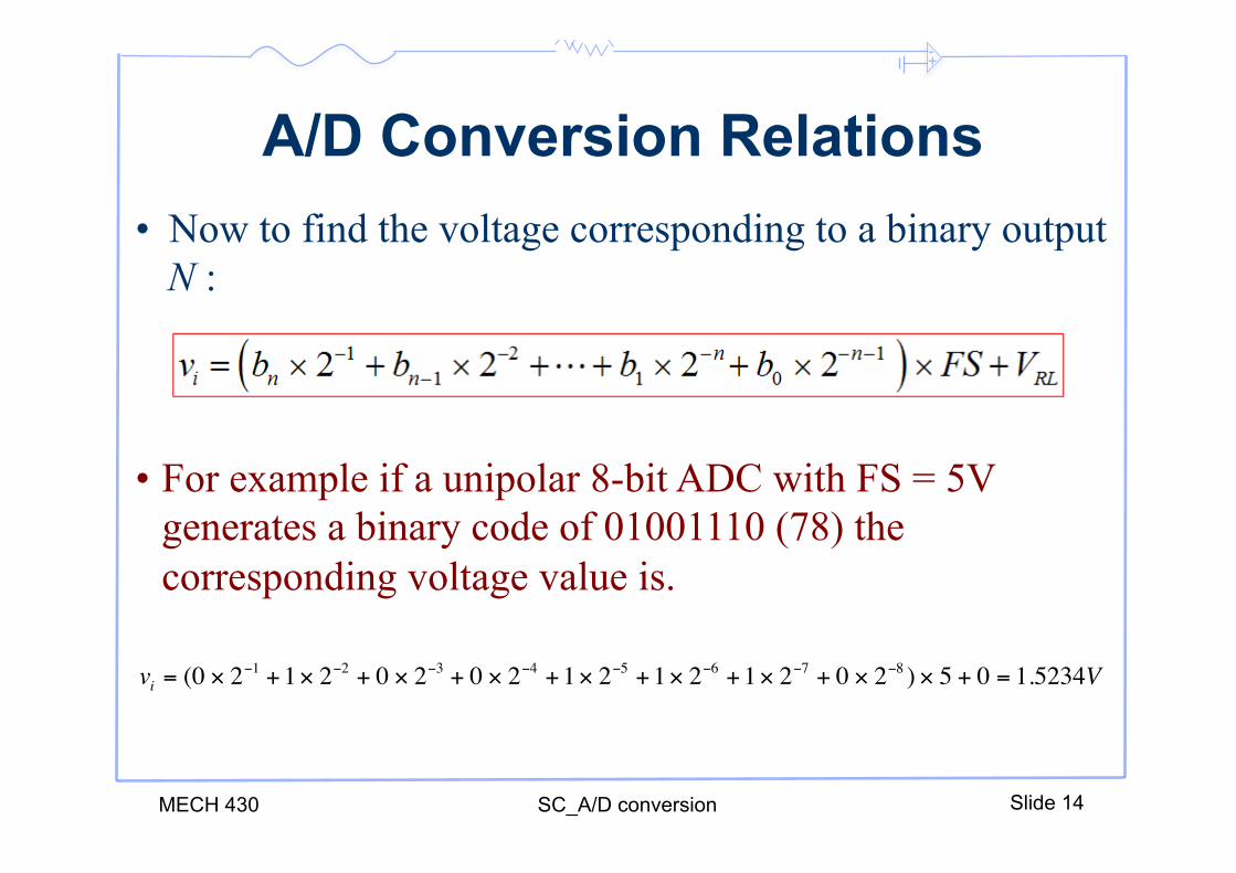
A/D Conversion Relations • Now to find the voltage corresponding to a binary output
N :
• For example if a unipolar 8-bit ADC with FS = 5V generates a binary code of 01001110 (78) the corresponding voltage value is.
vi = (0 × 2−1 +1× 2−2 + 0 × 2−3 + 0 × 2−4 +1× 2−5 +1× 2−6 +1× 2−7 + 0 × 2−8 ) × 5 + 0 = 1.5234V

- +
MECH 430 SC_A/D conversion Slide 15
Example 3 Minimum value
(Offset) Maximum
value Range (FS)
Unipolar A/D 0V 5V 5V
Bipolar A/D -2.5V +12.5V 15V 4-20 mA transmitters 4mA 20mA 16mA
k-bits VQ (%FS) LSB voltage for FS = 5V
4 6.25 312mV 8 0.3906 19.5mV 10 0.0977 4.90mV 12 0.0244 1.20mV 14 0.00610 305µV 16 0.00153 75µV

- +
Example 4 • Assume digitization of a unipolar signal that can change between 0 and 5
Volts into a 3 bit digital equivalent. Calculate the resolution, the number of quantized levels. (Answer: Res=0.625, Levels=8)
• Fill the table
• What is the maximum error that the output voltage can undertake? () • What will the maximum error be if we increased the number of bits to 4 in
the previous example? Verify that the error decreases with increasing the number of bits. ()
MECH 430 Introduction Slide 16

- +
Digital to Analog Conversion
• To find the analog voltage corresponding to the a specific output N, we use:
• Analog values within a quantum level generate the same output code. The maximum error is ±½LSB (Least Significant Bit). The error VE between the digitized voltage and the input voltage is estimated by:
• The error can be lowered by increasing the number of output bits of the converter
MECH 430 Introduction Slide 17
vi = N ×FS2k
"#$
%&'+VRL
- +
MECH 430 SC_A/D conversion Slide 18
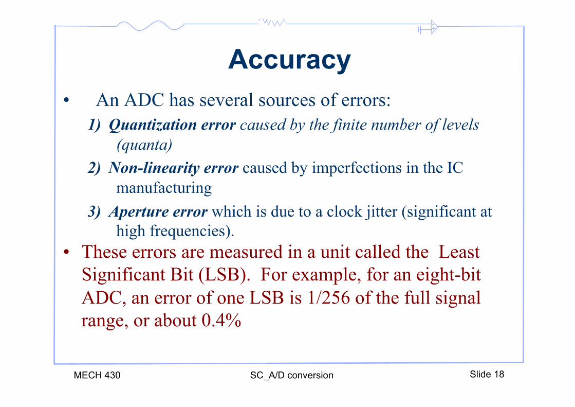
Accuracy • An ADC has several sources of errors:
1) Quantization error caused by the finite number of levels (quanta)
2) Non-linearity error caused by imperfections in the IC manufacturing
3) Aperture error which is due to a clock jitter (significant at high frequencies).
• These errors are measured in a unit called the Least Significant Bit (LSB). For example, for an eight-bit ADC, an error of one LSB is 1/256 of the full signal range, or about 0.4%

- +
MECH 430 SC_A/D conversion Slide 19
Quantization Error
• The quantization error is the error between the analog value and its digitized representation:
VE
Vx VQ
QXE NVVV −=
• The minimum number of bits required in the ADC for a specific allowable error VQ is (truncated to the next highest integer value):
k =log VMAX −VMIN[ ] /VQ +1( )
log(2)
- +
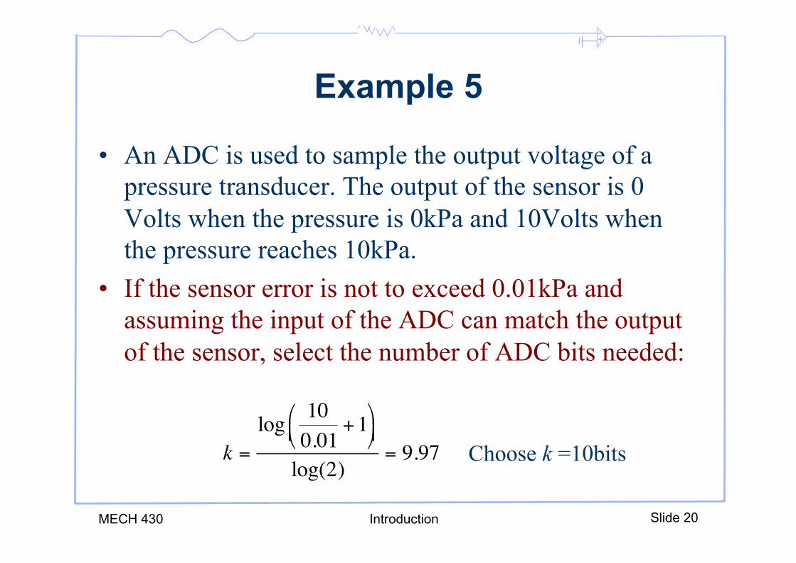
Example 5
• An ADC is used to sample the output voltage of a pressure transducer. The output of the sensor is 0 Volts when the pressure is 0kPa and 10Volts when the pressure reaches 10kPa.
• If the sensor error is not to exceed 0.01kPa and assuming the input of the ADC can match the output of the sensor, select the number of ADC bits needed:
MECH 430 Introduction Slide 20
k =log 10
0.01+1!
"#$%&
log(2)= 9.97 Choose k =10bits
- +
MECH 430 SC_A/D conversion Slide 21
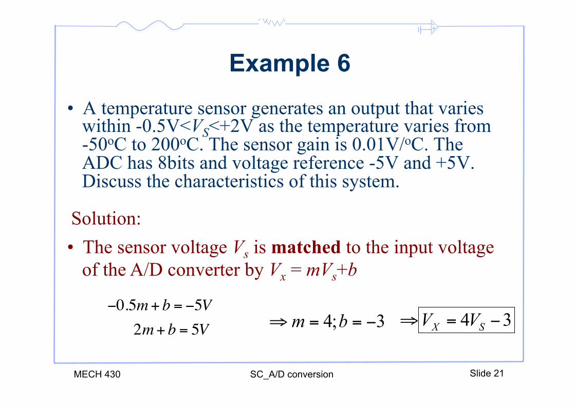
Example 6
• A temperature sensor generates an output that varies within -0.5V<VS<+2V as the temperature varies from -50oC to 200oC. The sensor gain is 0.01V/oC. The ADC has 8bits and voltage reference -5V and +5V. Discuss the characteristics of this system.
Solution: • The sensor voltage Vs is matched to the input voltage
of the A/D converter by Vx = mVs+b
−0.5m+ b = −5V 2m+ b = 5V 3;4 −==⇒ bm 34 −=⇒ SX VV

- +
MECH 430 SC_A/D conversion Slide 22
Example 6
Span: Step size: Resolution:
• For example at T = 50oC, the input of the ADC is: VX = [0.01V/oC) x 50oC]x4 - 3V = -1.0V
5.0-(-5.0V)=10.0V; 200oC-(-50oC)=250oC 10.0V/256 = 39.1mV; 250oC/256 = 0.98oC 39.1mV at 8-bit; 0.98 oC at 8-bit
The equivalent digital output is:
(-1.0V-(-5V))/(0.039V) = 102 (decimal) = 01100110 (binary)
• Therefore, the properties of this ADC are:
Number of quantized values
- +
MECH 430 SC_A/D conversion Slide 23
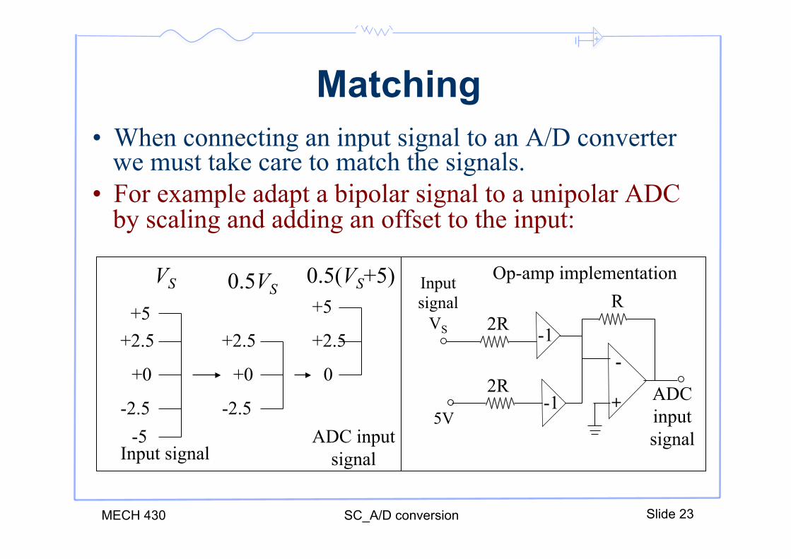
Matching • When connecting an input signal to an A/D converter
we must take care to match the signals. • For example adapt a bipolar signal to a unipolar ADC
by scaling and adding an offset to the input:
VS
+5 +2.5
+0
-2.5 -5
0.5VS
+2.5
+0
-2.5
+5
+2.5
0
0.5(VS+5)
Input signal ADC input
signal
+
-
-1
-1
Input signal
VS
5V
2R
2R
R
ADC input signal
Op-amp implementation
- +
MECH 430 SC_A/D conversion Slide 24
Example 7
Given: An IC temperature sensor with a gain of 5mV/oC is used to measure the temperature of an object up to 100oC. The sensor output is to be sent to an 8-bit ADC with a 0V-10V reference.
Find: Design the required signal conditioning to interface the sensor signal to the A/D and determine the temperature resolution.
- +
MECH 430 SC_A/D conversion Slide 25
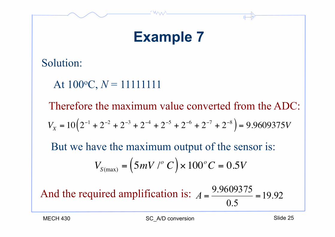
Example 7 Solution:
At 100oC, N = 11111111
Therefore the maximum value converted from the ADC:
VX = 10 2−1 + 2−2 + 2−3 + 2−4 + 2−5 + 2−6 + 2−7 + 2−8( ) = 9.9609375V
But we have the maximum output of the sensor is:
VS(max) = 5mV /o C( ) ×100oC = 0.5V
And the required amplification is: 92.195.0
9609375.9==A

- +
MECH 430 SC_A/D conversion Slide 26
Example 7
• This amplification may be implemented via a non-inverting op-amp with Rf = 18.92kΩ and Ri = 1kΩ
• Finally, the temperature resolution that is possible is:
ΔT =VQA
15mV /o C
=10 / 28( )19.92
15 10−3( )
= 0.39oC
amplification
resolution
gain

- +
MECH 430 SC_A/D conversion Slide 27
Sampling Rate • The analog signal is continuous in time and it is
necessary to convert this to a flow of digital values. • It is therefore required to define the rate at which new
digital values are sampled from the analog signal. • The rate of new values is called the sampling rate or
sampling frequency of the converter.
- +
MECH 430 SC_A/D conversion Slide 28
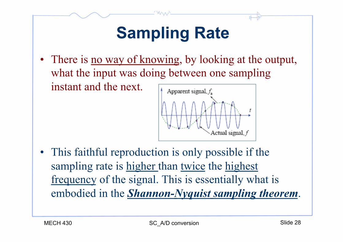
Sampling Rate • There is no way of knowing, by looking at the output,
what the input was doing between one sampling instant and the next.
• This faithful reproduction is only possible if the sampling rate is higher than twice the highest frequency of the signal. This is essentially what is embodied in the Shannon-Nyquist sampling theorem.

- +
MECH 430 SC_A/D conversion Slide 29
Sampling Rate • If the input is known to be changing slowly compared to
the sampling rate, then it can be assumed that the value of the signal between two sample instants was somewhere between the two sampled values.
• If, however, the input signal is changing fast compared to the sample rate, then this assumption is not valid.

- +
Aliasing • Aliasing is the misrepresentation of a high frequency
signal as a low frequency one. This might happen when we use an ADC as shown in the figure below.
• To avoid aliasing, the sampling frequency fs should be more than twice the highest frequency of the sampled analog signal. The sampling frequency of the analog signal fo affects the accuracy of the discrete time representation of the signal. For a reliable approximation, the sampling frequency should be 5 to 10 times the analog signal frequency
MECH 430 Introduction Slide 30

- +
Aliasing
MECH 430 Introduction Slide 31
TS
T0
fS = 1/TSSamplingtimesf0 = 1/T0
Apparent signal(frequency fA)
- +
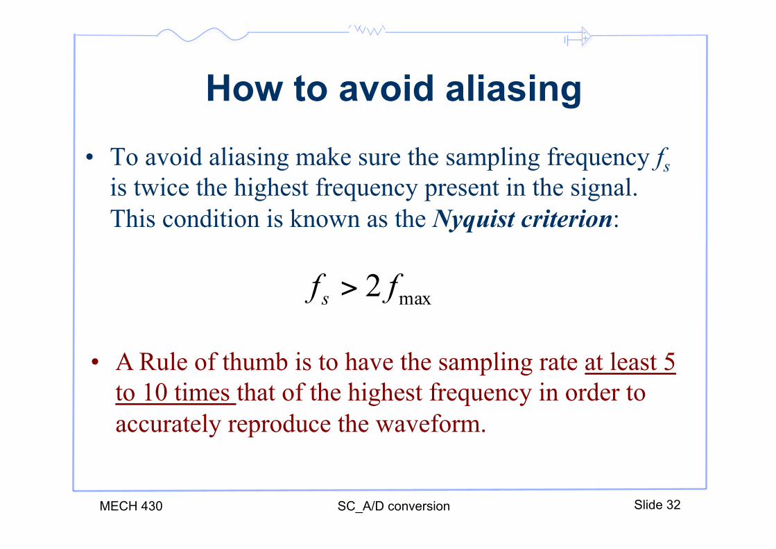
MECH 430 SC_A/D conversion Slide 32
How to avoid aliasing
• To avoid aliasing make sure the sampling frequency fs is twice the highest frequency present in the signal. This condition is known as the Nyquist criterion:
max2 ffs >
• A Rule of thumb is to have the sampling rate at least 5 to 10 times that of the highest frequency in order to accurately reproduce the waveform.