instruction manual model 225 current source -...
TRANSCRIPT
Instruction Manual Model 225
Current Source
Publication Date: August 1976 Keithley Instruments, Inc.
Cleveland, Ohio, U.S.A. Document Nufnber: 29039

WARRANTY
Keithley Instruments, Inc. warrants this product to be free from defects in material and workmanship for a period of 1 year from date of shipment.
Keithley Instruments, Inc. warrants the following items for 90 days from the date of shipment: probes, cables, rechargeable batteries, diskettes. and documentation.
During the Wmanty period, we will, at OUT option, either repair or replace any product that proves to be defective.
To exercise this warranty, write or call your local Keithley representative, or contact Keithley headquarters in Cleveland, Ohio, You will be given prompt assistance and return instructions. Send the product, transportation prepaid, to the indicated service facility. Repairs will be made and the product returned, transportation prepaid. Repaired or replaced products are warranted for the balance of the origi- nal warranty period, or at least 90 days.
LIMITATION OF WARRANTY
This warranty does not apply to defects resulting from product modification without Keithley’s express written consent, or misuse of any product or part. This warranty also does not apply to fuses, software, non-rechargeable batteries, damage from battery leakage, or problems arising from normal wear or failure to follow instructions.
THIS WARRANTY IS IN LIEU OF ALL OTHER WARRANTIES, EXPRESSED OR IMPLIED, INCLUDING ANY IMPLIED WARRANTY OF MERCHANTABILITY OR FITNESS FOR A PARTICULAR USE. THE REMEDIES PROVIDED HEREIN ARE BUYER’S SOLE AND EXCLUSIVE REMEDIES.
NEITHER KEITHLEY INSTRUMENTS, INC. NOR ANY OF ITS EMPLOYEES SHALL BE LIABLE FOR ANY DIRECT, INDI- RECT, SPECIAL, INCIDENTAL OR CONSEQUENTIAL DAMAGES ARISING OUT OF THE USE OF ITS INSTRUMENTS AND SOFTWARE EVEN IF KEITHLEY INSTRUMENTS, INC., HAS BEEN ADVISED IN ADVANCE OF THE POSSIBILITY OF SUCH DAMAGES. SUCH EXCLUDED DAMAGES SHALL INCLUDE, BUT ARE NOT LIMITED TO: COSTS OF REMOVAL AND INSTALLATION, LOSSES SUSTAINED AS THE RESULT OF INJURY TO ANY PERSON, OR DAMAGE TO PROPERTY.
CONTENTS MODEL 225
CONTENTS
SP*CIFICATIONS---------------------------------------------------------------------
1. GENERAL DESCRIPTION------------------------------------------------------------
2. OPERATION----------------------------------------------------------------------
3. CIRCUIT DESCRIPTION------------------------------------------------------------
4. ACCESSORIES--------------------------------------------------------------------
5. SER”ICING----------------------------------------------------------------------
lj. CALIBRATION--------------------------------------------------------------------
7. REPLACEABLE PARTS--------------------------------------------------------------
SCH~rIC------------------------------------------------------------------------
1
2
4
8
10
11
12
19
31
ii 3
ILLUSTRATIONS
ILLUSTRATIONS
I Figure NO. Title Page
1 Prone Panel. ............................ 1
2 Front Panel Controls ........................ 3
3 Rear Panel Controls. ........................ 3
4 Connections. ............................ 4
5 Resistive Load ............................ 6
6 Currenf Sink ............................ 6
7 Capacitive Load. .......................... 6
8 Inductive Load ........................... 6
9 Floating Supply. .......................... 6
10 Volt Limit Characteristic. ..................... 7
11 Modulation ............................. 7
12 Block.Diagram. ........................... 8
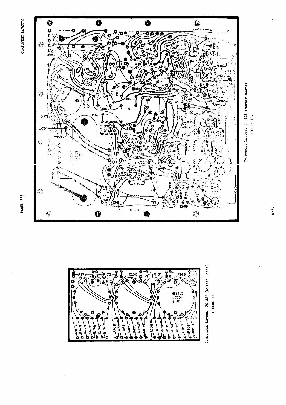
13 Component Layout, PC-227 (Switch Board). .............. 13
14 Component Layauc, PC-228 (Mother Board). .............. 13
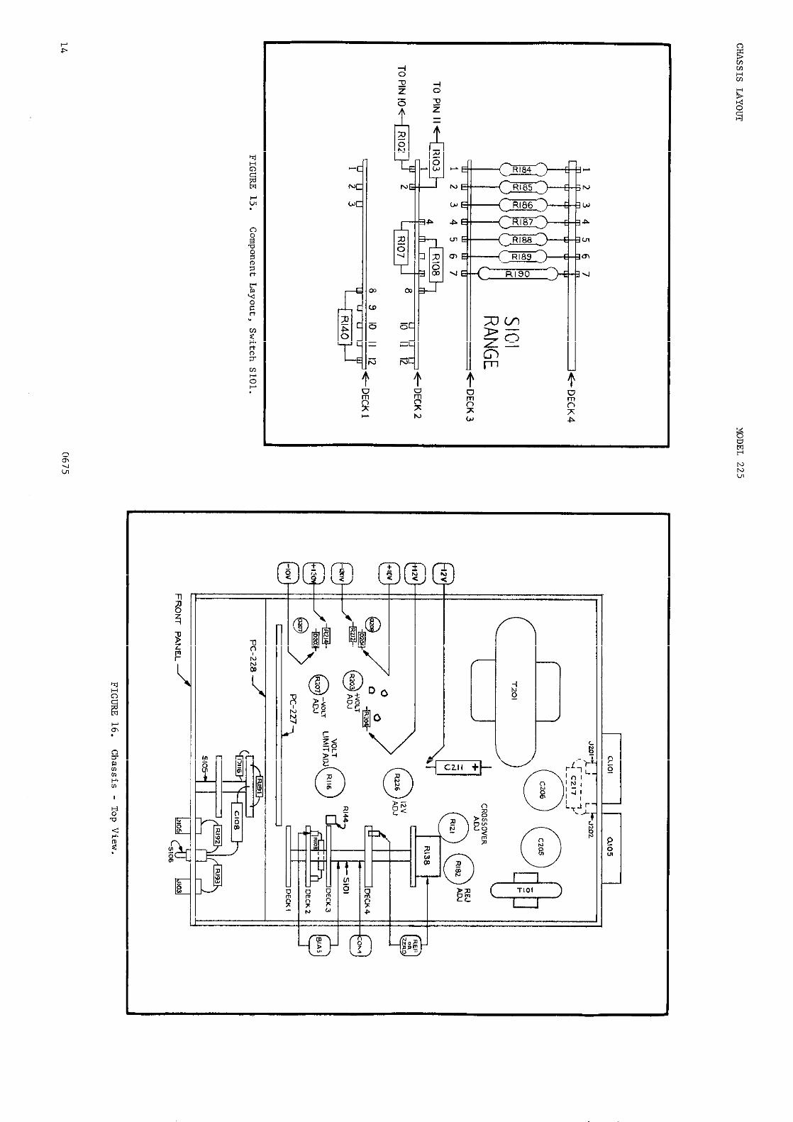
15 Component Layout, Switch 5101. ................... 14
16 Chassis - Top View ......................... 14
17 Accuracy Check ........................... 18
18 Regulation Check .......................... 18
19 Modulation Check .......................... 18
20 Inductive Load Check ........................ 18
21 current Mode "S Voltage Made Waveforms ............... 18
22 Top Cover Assembly ......................... 21
23 Bortom Cover Assembly. ....................... 21
I
0676 iii
4
CAUTION
CAUTION
MODEL 225
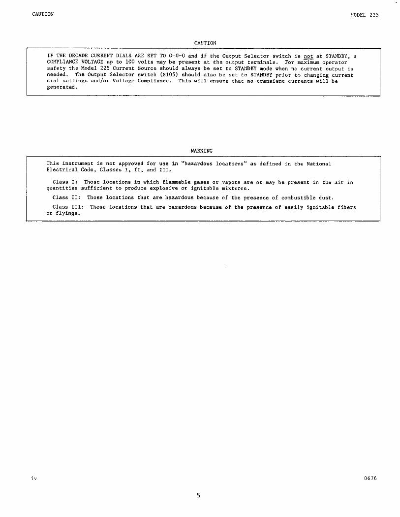
IF THE DECADE CURRENT DIALS ARE SET TO O-O-O and if the Output Selector switch is not at STANDBY, a COMPLIANCE VOLTAGE up to 100 volts may be present at the oucpuc terminals. For r&x"rn operator safety the Model 225 Current Source should always be set to STA!IDBY mode when no current output is needed. The Output Selector switch (S105) should also be set to STANDBY prior to changing current dial seteings and/or Voltage Compliance. This will ensure that no transient currente will be generated.
WARNING
This insrrument is no? approved for use in "hazardous locations" as defined in the National Electrical Code, Classes I, II, and III.
Class I: Those locations in which flameble gases or vapors are or may be present in the air in quantifies sufficient to produce explosive or ignitable mixcures.
Class II: Those locations that are hazardous because of the presence of combustible dust.
Class III: Those locations that are hazardous because of the presence of easily ignitable fibers or flyings.
0676
5
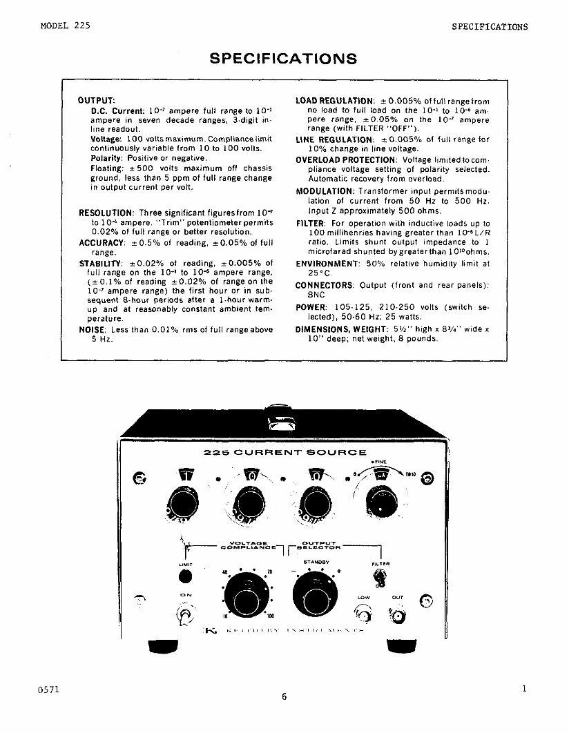
MODEL 225 SPECIFICATIONS
SPECIFICATIONS
OUTPUT: D.C. Current: lo-’ ampere full range to lo-’ ampere in seven decade ranges, 3.digit in. line readout. Voltage: 100 voltsmaximum. Compliancelimit continuously variable from 10 to 100 volts. Polarity: Positive or negative. Floating: c 500 volts maximum off chassis ground, less than 5 ppm of full range change in output current per volt.
RESOLUTION: Three significant figuresfrom lo-’ to 10-l ampere. “Trim” potentiometer permits 0.02% of full range or better resolution.
ACCURACY: z 0.5% of reading. 2 0.05% of full ra”ge.
STABILITY: -0.02% of reading, _cO.O05% of full range on the 10-l to 1O-6 ampere range, (e-0.1% of reading 20.02% of range on the 10-T ampere range) the first hour or in sub. sequent E-hour periods after a l.hour warm- up and at reasonably constant ambient tern. perature.
NOISE: Less than 0.01% rms of full rangeabove 5 HZ.
LOADREGULATION: t0.005% offullrangefrom no load to full load on the lo-’ to 10-6 am. pere range, 50.05% on the lo-’ ampere range (with FILTER “OFF”).
1
LINE REGULATION: k 0.005% Of full range for 10% change in line voltage.
OVERLOAD PROTECTION: Voltage limited tocorn. pliance voltage setting of polarity selected. Automatic recovery from overload.
MODULATION: Transformer input permitsmodw lation of current from 50 Hz to 500 Hr. Input 2 approximately 500 ohms.
FILTER: For operation with inductive loads up to 100 millihenries having greater than 10.6L/R ratio. Limits shunt output impedance to 1 microfarad shunted bygreaterthan 1010ohms.
ENVIRONMENT: 50% relative humidity limit at 25’C.
CONNECTORS: Output (front and rear panels): BNC
POWER: 105.125, 210.250 volts (switch se. lected), 50.60 Hz; 25 watts.
DIMENSIONS, WEIGHT: 5%” high x 8%” wide x 10” deep; net weight, 8 pounds.
225 CURRENT SOURCE .IWE
0571 6
1
GENERAL DESCRIPTION
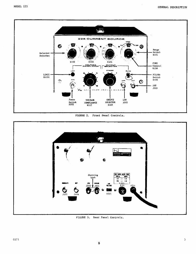
SECTION 1. GENERAL DESCRIPTION
MODEL 225
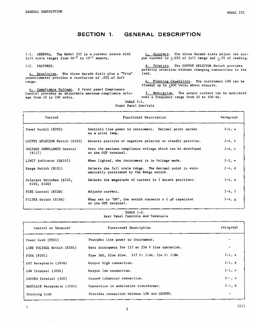
1-I. GENERAL. The Model 225 is a current source with full scale ranges frarn 10-7 to 10-l ampere.
1-2. FEATURES.
a. Resolution. The thpe decade dials plus a "Trim" potentiometer provides a resolution of .02% of full range.
b. Compliance Voltage. A front panel Compliance Cantral provides a" adjustable maximum compliance volt- see from 10 to 100 volts.
c. Accuracy. The three decade dials adjust the out- put current to +.05% of full range and +.5% of reading.
d. Polarity. The OUTPUT SELECTOR Switch provides polarity selection without changing connections c" the load.
e. Floating Capability. The instrument LOW can be floated up t" 2500 volts above chassis.
f. Modulation. The ""tput current can be modulated over a frequency range from 50 t" 500 Hz.
TABLE l-l. Front Panel Controls
CQ"trOl Punctianal Description Paragraph
Power Switch (S202) Controls line power to instrument. Decimal point serves 2-4, a as a pilot lamp.
OUTPUT SELECTOR Switch (SlO5) Selects positive or negative polarity or standby pasitio". 2-4, b
VOLTAGE COMPLIANCE Control Sets the maximum compliance voltage which can be developed 2-4, c (R117> at the OUT terminal.
LIMIT Indicator (DSlOl) When lighted, the instrument is in Voltage mode. 2-2, e
Range Switch (SlOl) Selects the full scale range. The decimal point is auto- 2-4, d matically positioned by the Range switch.
Selectar Switches (S102, Selects the magnitude af current in 3 decade positions. 2-4, e s103, SlO4)
FINE Control (R13S) Adjusts current. 2-4, f
FILTER Switch (5106) When set to "ON", the switch connects a 1 p capacitor 2-4, s at the OUT terminal.
TABLE 1-2. Rear Panel Controls end Termirals
Control or Terminal Functional Description Paragraph
Power Cord (P201) Pravides line power to instrument.
LINE VOLTAGE Switch (S201) Sets instrument for 117 or 234 V line operatia".
FUSE (F201) Type 3AG. slow slow. 117 v: 1,4A; 234 Y: l/S‘4 2-1, a
OUT Receptacle (3104) Output high cannectio". 2-1, a
LOW Terminal (5201) Output law connection. 2-1, a
GROOND Terminal (520) Ground (chassis) connection. 2.1, a
!4ODUlATE Receptacle (5101) Connection to modulation transformer. 2-1, b
Shorting Link Provides cbnnection between LOW and GROUND.
7 7
0571
MODEL 225 GENERAL DESCRIPTION
0571 3 8
OPERATION MODEL 225
SECTION 2.
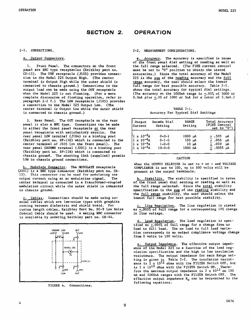
2-l. CONNECTIONS.
8. OUtPUt conneerors.
1. Front Panel. The connectors on the front panel are BNC type receptacles (Keithley part no. cs-15). The OVP receptacle (5103) provides conr,ec- tion to the Model 225 Output High. (The center terminal is Output High while the outer shield is connected to chassis ground.) Connections to the output load can be made using the OUT receptacle when the Model 225 is not floating. (For a more complete discussion of floating operation, refer to paragraph 2-2 f.) The LOW receptacle (JlO5) provides a connection to the Model 225 Output Low. (The center terminal is Output Low while the outer shield is connected to chassis ground.)
2. asac Panel. The OUT receptacle on the rear panel is also a BNC type. Connections can be made to either the front panel receptacle s the rear panel receptacle with satisfactory results. The rear panel LOW terminal (3104) is a binding post (Keithley part no. BP-1lG) which is connected to the center terminal of 5105 (on the front panel). The rear panel GROUND terminal (3201) is a binding past (Keithley part’no. BP-118) which is connected to chassis ground. The shorting link (supplied) permits LOW to chassis ground connections.
b. Modulate Connector. The NOD”UTE receptacle 0101) is a BNC type connector (Keithley part no. CS- 15). This connector can be used for modulating the output current using an ac modulation signal. The center terminal is connected to a transformer-coupled modulation circuit while the outer shield is connected to chassis ground.
c. Cables. Connections should be made using co- axial cables which are low-noise types with graphite coating between dielectric and shield braid. For custom length cables, Keithley Part No. SC-9 Low Noise Coaxial Cable should be used. A mating BNC connector is available by ordering Keithley part no. CS-44.
OPERATION
2-2. MEASUREMENT CONSIDERATIONS.
a. Accuracy. The accuracy is specified in terms of the front panel dial setting or reading as well as the full range selected. (The FINE current control must be set to “0” position to obtain the stated accuracies.) Since the total accuracy of the Model 225 is the s of the readina accuracy and the full a accuracy, the user should select the lowest full range for best possible accuracy. Table 2-l. shows the total accuracy for typical dial settings. (The accuracy on the lOOkA range is +.05% of 1000 or o.s”A plus 2.5% of 1000 or %A for a coca1 of 5.5nA.)
TABLE 2-l. Accuracy For Typical Dial Settings
Output Decade Dial RANGE Total Accuracy lhrL-elLt setting Setting (FINE c0ntr01
set to “0”)
1 x lo-6A o-o-1 1000 &k4 + .505 VA 1 x lo-6A O-1-0 100 $ + .055 NA 1 x 10⁴A 1-o-o 1 x lo-6A
10 @ + .OlO * 10-O-O 1000 UA + .0055 p.4
CAUTION CAUTION
When the OUTPUT SELECTOR is set to + or - and VOLTAGE When the OUTPUT SELECTOR is set to + or - and VOLTAGE COMPLIANCE is set to 100, up to 100 volts will be COMPLIANCE is set to 100, up to 100 volts will be present at the output terminals. present at the output terminals.
b. Stability. The stability is specified in terms of the front panel dial setting or reading as well as the full range selected. Since the m stability specification is the e of the readinR stability and the full range stability, the user should select the lowest full range for best possible stability.
c. Line Regulation. The line regulation is stated as +..005% of full range for a corresponding 10% change in line voltage.
d. Load Rezulation. The load regulation is spec- ified a8 2.005% of full range far a change from no load to full load. The no load to full load varia- tion corresponds to an output compliance voltage change from 0 volts to 100 volts.
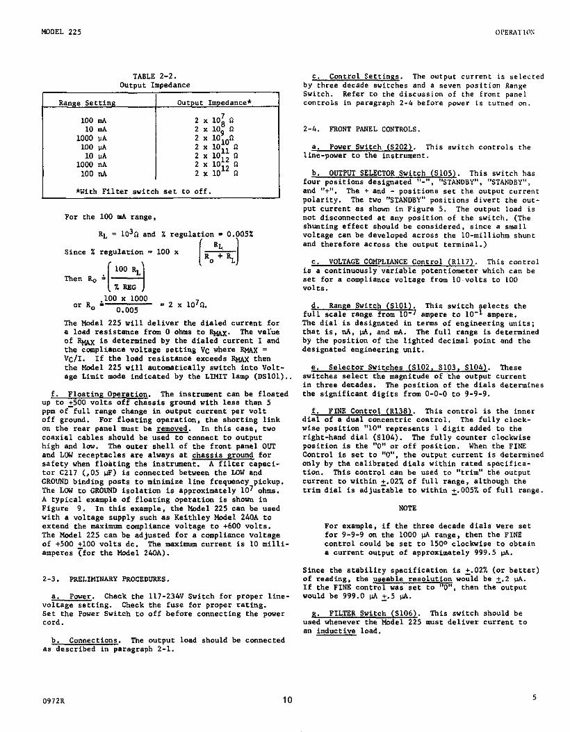
e. Output Impedance. The effective output imped- ance of the Model 225 is a function of the load reg- ulation specification and the high to low insulation resistance. The output impedance for each Range set- ting is given in Table 2-2. The insulation resist- ance is 2 x 10¹² ohms with the FILTER Switch OFF, but is 1 x lOlo ohms with the’FILTER Switch ON. There- fore the maximum output impedance is 2 x lOl2 on 100 nA and 1OOOti ranges with the FILTER Switch OFF. The effective output impedance R. ~a” be decermtned by the following equations.
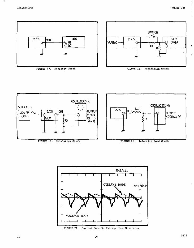
FIGURE 4. Co”*ectm”s.
0676
MODEL 225
2 x 10; n 2 x log n 2 x lOlOG 2 x 1OlI R
2 x l0l2 “, “, : :;12 n
TABLE 2-2. Output Impedance
Range setting O”tput Impedance*
100 m.4 10 mA
1000 liA 100 ,,A 10 UA
1000 nA 100 nA
*With Filter switch set to off. I
For the 100 mA range,
R,, = 103n and % regulation = 0.005%
since I regulation = 100 x RL
I 1 qq
Then % -
The Model 225 will deliver the dialed current for a load resistance from 0 ohms to WK. The val’ue of w is determined by the dialed current I and the compliance voltage setting VC where Rw.K = WI. If the load resistance exceeds RMAx then the Mcdel 225 will automatically switch into Volt- age Limit mode indicated by the LIMIT lamp (DSlOl)..
f. Floatiw Operation. The instrument can be floated “I) to +500 volts off chassis nround with less than 5 ppm of-full range change in &put current per volt off ground. For floating operation, the shorting link on the rear panel m,,st be m. In this case, two coaxial cables should be used to connect to output high and low. The outer shell of the front panel O!Jf and LOW receptacles are always at chassis ground for safety when flokting the instrument. A filter capaci- tor C217 (,05 ~0 is connected between the LOW and GROUND binding posts to minimize line frequency pickup. The LOW to GROUND isolation is approximately lo7 ohms. A typical example of floating operation is shown in Fig”re 9. In this example, the Model 225 can be used with a voltage supply such 8s Keithley Model 240A to extend the maximum compliance voltage to +600 volts. The Model 225 can be adjusted for a compliance voltage of +500 2100 volts de. The maximum current is 10 milli- amperes (for the Model 24OA).
2-3. PRELIMINARY PROCEDURES.
a. Power. Check the 117-234V Switch for proper line- voltage setting. Check the fuse for proper rating. Set the Power Switch to off before connecting the power card.
b. Connections. The output load should be cwnected as described in paragraph 2-l.
c. contra1 setti”*s. The output current is selected by three decade switches and a seven position Range Switch. Refer to the discussion of the fronr panel concrok in paragraph 2-4 before power is turned on.
2-4. FRONT PANEL CONTROLS.
a. Power Switch (S2022. This switch controls the line-power to the instrument.
b. OUTPUT SELECTOR Switch (SlO5). This switch has four positions designated “-“, “STANDBY”, “STANDBY”, and “+“. The + and - positions set the output current polarity. The two “STANDBY” positions divert ehe out- put current as shown in Figure 5. The output load is not disconnected at any position of the switch. (The shunting effect should be considered, since a small voltage can be developed across the lo-milliahm shunt and therefore across the output terminal.)
c. VOLTAGE COMPLIANCE Control (R1171. This control is a continuously variable potentiometer which can be see for a compliance voltage from lo~volts to 100 volts.
d. Range Switch (SlOl). This switch selects the full scale ranpe from 10-7 BmDePe to 10-l amoere. The dial is deiignated in re&s of engineering Airs; that is, nA, IJA, and mA. The full range is determined by the position of the lighted decimal point end the designated engineering unit.
e. Selector Switches (SIOZ, SlO3. S104L. These switches select the magnitude of ‘the o”tput current in three decades. The position of the dials determines the significant digits from O-O-O to V-9-9.
f. FINB Control (Rl38)-. This control is the inner dial of a dual concentric control. The fully clock- wise position “10” represents 1 digit added t., the right-hand dial (S104). The fully counter clockwise position is the “0” or off position. When the FINE Control is set to “0”. the output current is determined only by the calibrated dials within rated specifica- tion. This control cm be used to “trim” the output current to within +.02% of full range, although the trim dial is adjustable t., within 2.005% of full range.
NOTE
For example, if the three decade dials were set for 9-9-9 on the 1000 !,A range, then the FINE control could be set to 1500 clockwise to obtain a current .Y”tp”t of approximately 999.5 +4.
Since the stabilitv specification is +.02% (or better) of reading, the useebie resolution w&d be ~i.2 ,,A. If the FINE control was set to “O”, then the output would be 999.0 ti 2.5 ,JA.
g. FILTER Switch (S106). This switch should be used whenever the Model 225 must deliver current to an inductive load.
0972B 10 5
OPERATION MODEL 225
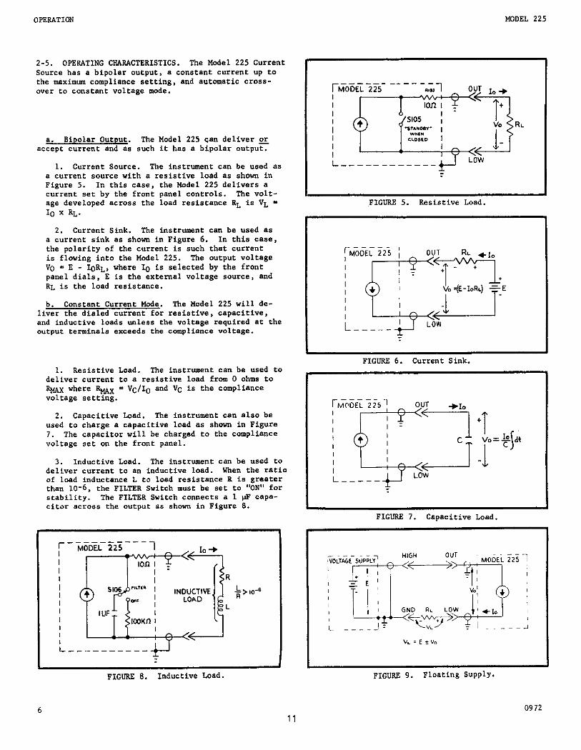
2-5. OPERATING CHARACTERISTICS. The Model 225 Current Source has a bipolar output, a constant cnreent up to the maximum compliance setting, and automatic cross- over to constant voltage mode.
a. Bipolar Output. The Model 225 can deliver 0’ accept current and as such it has a bipolar output.
1. Current Source. The instrument can be used as a current source with a resistive load as shown in Figure 5. In this case, the Model 225 delivers B current set by the front panel controls. Tbe volt- age developed across the load resistance RL is V, = IO x RL.
2. Current Sink. The instrument can be used as a current sink as shown in Figure 6. In this case. the polarity of the current is such that cw’eent is flowing into the Model 225. The output voltage “0 = E - IORL, where IC is selected by the front panel dials, E is the external voltage source, and RL is the load resistance.
b. Constant Current Mode. Tbe Model 225 will de- liver the dialed current for resistive, capacitive, and inductive loads unless the voltage required at the output terminals exceeds the compliance voltage.
1. Resistive Load. The instrument can be used to deliver current to a resistive load from 0 ohms to w where k = VC/IO and VC is the compliance voltage setting.
2. Capacitfve Load. The instrument can also be used to charge a capacitive load as shown in Figure 7. The capacitor will be charged to the compliance voltage set on the front panel.
3. Inductive Load. The instrument can be used to deliver current to an inductive load. When the ratio of load inductance L to load resistance R is greeter than 10-6, the FILTER Switch m”st be set to “ON” for stability. The FILTER Switch connects a 1 pF cap*- citor across the output as shown in Figure 8.
:- I I I I
I
FIGURE 8. Inductive Load.
-‘Iff!?++iJ RI ___----------
I
FIGURE 5. Resistive Load.
I FIGURE 6. Current Sink.
FIGURC 7. Capacitive Load.
FIGURE 9. FIGURE 9. Floating Supply. Floating Supply.
6 11
0972
MODEL 225 OPERATION
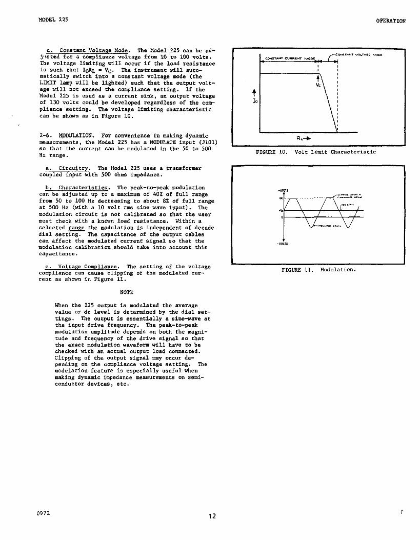
C. constant “Oltsge Mode. The Model 225 can be ed- jwted for a compliance voltaza from 10 to 100 volts. The voltage limiiing will o&r if the load resistance is such that IORL - "C. The instrument "ill auto- marically switch into a constant voltage mode (the LIMIT lamp will be lighted) such that the output volt- age will not exceed the compliance setting. If the Mcdel 225 is used as a current sink, a,, output voltage of 130 volts could be developed regardless of the con- pliance setting. The voltage limiting characteristic can be shown as in Figure 10.
t 1.3
I 2-6.
, M!JDULATION. For convenience in making dynamic
measurements, the Model 225 has a MODULATE input (JlOl) I RL-+
so that the current can be modulated in the 50 to 500 I
HZ range. F1mP.E 10. Volt Limit Characteristic
a. Circuirry. The Model 225 uses a transformer coupled input with 500 ohms impedance.
b. Characteristics. The peak-to-peak modulation can be adjusted up to a maximum of 40% of full range from 50 CD 100 Hz decreasing to about 8% of full range at 500 Hz (with a 10 volt rms sine wave input). The modulation circuit is not calibrated so that the user m"st check with a knwn load resistance. Within a selected w the modulation is independent of decade dial setting. The capacitance of the output cables can affect the modulated current signal so that the modulation calibration should take into account this CapC.CitaWX.
I I C. "Olcage Complia*ce. The serring of the voltage
compliance can cause clipping of the modulated cur- FIGURE 11. Modulation. rent as shovn in Figure 11.
NOTE
When the 225 output is modulated the average value or dc level is determined by the dial set- rings. The outpllt is essentially a sine-wave at the input drive frequency. The peak-to-peak modulation amplitude depends on both the magni- tude and frequency of the drive signal so that the exact modulation waveform will have to be checked tith an actual output load connected. Clipping of the output signal may occur de- pending on the compliance voltage setting. The modulation feature is especially useful when making dynamic impedance measurements on semi- conductor devices, etc.
0972 12 7
CIRCUIT DESCRIPTION
SECTION 3. CIRCUIT DESCRIPTION
MODEL 225
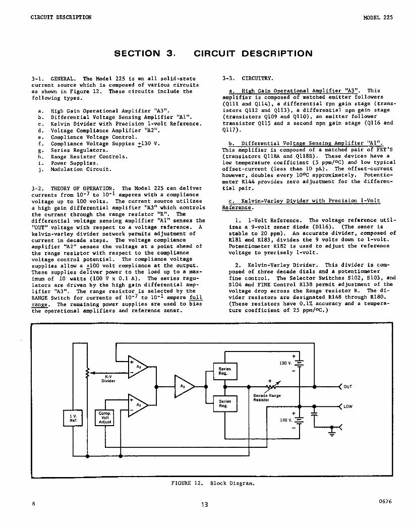
3-1. GENERAL. The Model 225 is an all solid-state current source which is composed of varicus circuits as shown in Figure 12. These circuits include the following types.
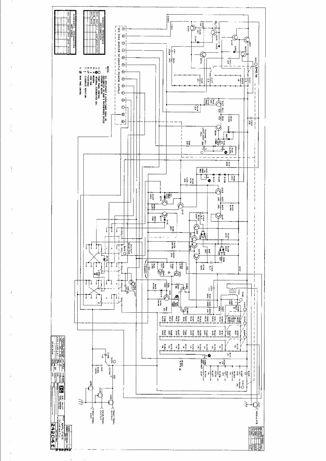
a. High Gain Operational Amplifier “A3”. b. Differential Voltage Sensing Amplifier “Al”. c. Kelvin Divider with Precision l-volt Reference. d. Voltage Compliance Amplifier ‘A2”. e. Compliance Voltage Control. f. Compliance Voltage Suppies 2130 V. g. Series Regulators. h. Range Resistor Controls. i. Power Supplies. j. Modulation Circuit.
3-2. THEORY OF OPERATION. The Model 225 can deliver currents from 10-7 to 10-l amperes with a compliance voltage up t0 100 volts. The current source utilizes a high gain differential amplifier “A3” which controls the current through the range resistor “R”. The differential voltage sensing amplifier ‘Al” senses the “OUT” voltage with respect to a voltage reference. A kelvin-varley divider network permits adjustment of current in decade steps. The voltage compliance amplifier ‘AZ” eenses the voltage at a point ahead of the range resistor with respect to the compliance voltage contra1 patenrial. The compliance voltage supplies allw a 2100 volt compliance at the output. These supplies deliver power to the load up to B mex- imm of 10 watts (100 V x 0.1 A). The series regu- lators are driven by the high gain differential amp- lifier ‘A3”. The range resistor is selected by the RANGE Switch for currents of 10-7 ta 10-l ampere full w. The remaining power supplies are used to bias the operational amplifiers and reference zener.
3-3. CIRCUITRY.
a. High Gain Operational Amplifier ‘A3”. This amplifier is composed of matched emitter followers (4111 and Q114). e differential rpn gain stage (trans- istors Qlli and Q113), a differential npn gain stage (transistors QlOS and QllO), an emitter follower transistor Q115 and a second npn gain stage (Q116 and Ql17).
b. Differential Voltage Sensing Amplifier “Al”. This amplifier is composed of a marched pair of FET’S (transistors Q118A and Q118B). These devices have a low temperature coefficient (5 ppm/W) and low typical offset-current (less than 10 pA). The offset-current however, doubles every 10°C approximately. Potentia- meter R144 provides zero adjustment for the differen- tial pair.
c. Kelvin-Varley Divider with Precision l-Volt Reference.
1. l-Volt Reference. The voltage reference util- izes a S-volt zenee diode (D116). (The zener is stable to 20 ppm). An accurate divider, composed of R181 and R183, divides the 9 volts down to l-volt. Potentiameter R182 is used to adjust the reference voltage ta precisely l-volt.
2. Kelvin-Varley Divider. This divider is com- posed of three decade dials and a potentiometer fine control. The Selector Switches 5102, S103, and S104 and PINE Control Rl38 permit adjustment of the voltage drap across the Range resistor R. The di- vider resistors are designated R148 through R18D. (These resistors have 0.1% accuracy and a tempera- ture coefficient of 25 ppmlW.)
FIGURE 12. Block Diagram.
0676
MODEL 225
d. Voltage Compliance Am”lifier ‘A2”. This ampli- fier is comwsed of a differential nain staee: trans- istors Q107’and QlO8. The fr”“t p&e1 compii&ce con- trol R117 sets the maximum compliance voltage desires up to +100 volts. The bias reference for transistor QlO8 is provided by a divider string camposed of re- sistors Rl15, R116, R117, and R118. Potentiometer R116 provides a” internal compliance voltage edjust- ment. The amplifier is biased “off” in the constant- current mode of operatian. When the voltage at the “series regulator output” reaches the preselected CMI\- pliance limit, the amplifier “A2” is t”rned “ON” and the Model 225 automatically changes to a voltage limit made. The LIMIT indicator US101 is turned on a”t”- matically when in the “valtage limit mode”. F”r pos- itive polarity, transistor QlO8 turns on in the volt- age limit mode while 4107 is turned aff. The differ- ence voltage is buffered by emitter-follower stage, Q201 and Q204. Transistor Q202 is turned on and chere- fore drives transistor Q207. (The LIMIT indicator is cannecced in series with Q207.) Transistor Q2D2 pro- vides valtage level translation. Far negative polar- ity, the difference voltage between Q107 and Q108 is such that transistors 4205 and QZO6 are driven. (Transistors Q201 and 9204 act as buffer stages.) Transistor Q206 provides voltage level translation and drives Q208. The LIMIT indicator is connected in series with Q208 and is turned an. Potentiometers R203 and R207 provide control of the LIMIT indicator turn-on for + limit and - limit respectively.
e. Compliance VoltaRe Control. This control adjusts the maximum compliance voltaee from +lO volts t” cl00 Volts. This is’accomplishedwby “sing a linear 5D-kil- ohm potentiometer designated R117. A constant c”rrent is driven through the resistor divider. The polarity is controlled by the ODTPIPT SELECTOR Switch S105.
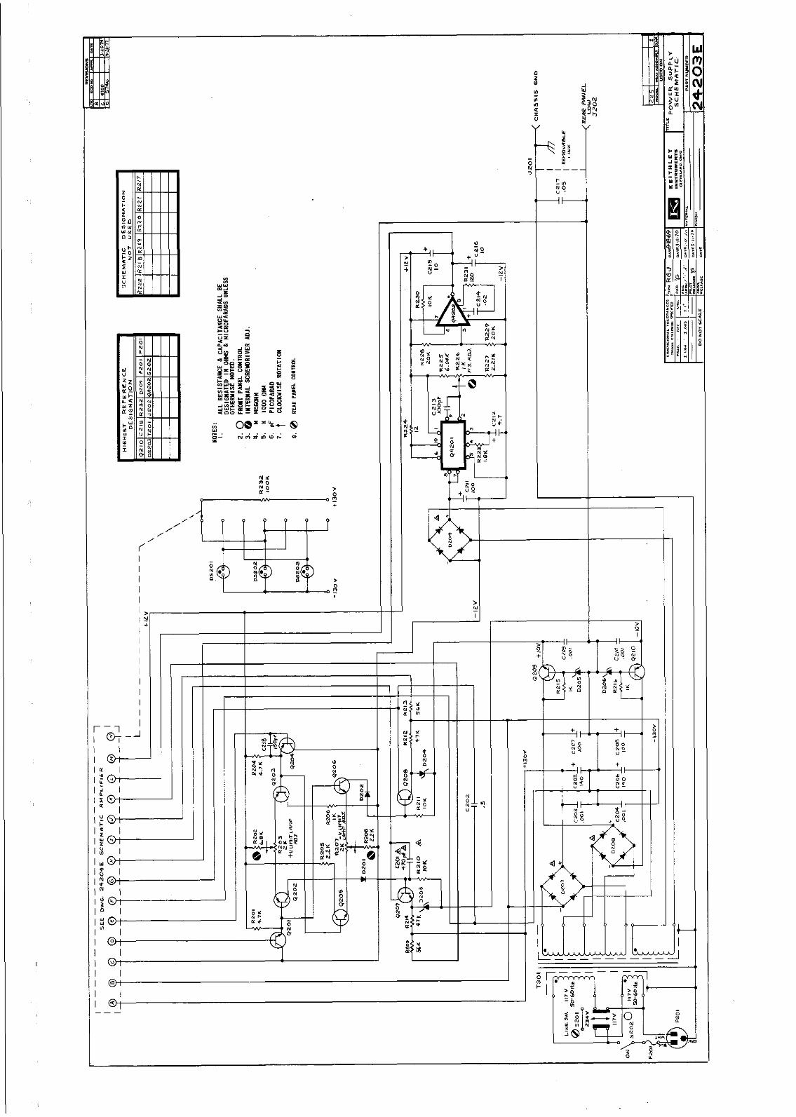
f. Compliance Voltage Supplies. These voltage suoolies orovide unresulated +130 volts for the series .~ regulatarb. AC pover”is obe&ed fram a secondary of transformer T201. Diodes D207 thru D21D form a full- wave rectifier. Capacitors C203 thru C206 provide filtering of *c ripple.
g. Series Resulators. Transistors QlOl and 9105 form a comolimentarv-svmmetrv 0”tp”t staw. (These transistor; are rated at 300.vol&, 35 watts.) Tran- sistors Q103 and 9106 are c”rrent limiting transistors which shut down the output transistors during a change in the selected polarity.
h. Range Resistor Controls. The Range Switch SlOl selecees full range current fram lop7 to 10-l amperes. Range resistors R184 thr” R190 are selected such that, for each selected current, the voltage drop across the Range resistor R is 1 volt for full range.
CIRCUIT DESCRIPTION
i. Power Supplies. The remaining power supplies provide power to the amplifier stages and voltage references.
1. 510 volts. Diodes D211 tbr” D214 form a fu.ll- wave rectifier which provides unregulated voltages for the 210 vole regulator stages. Capacitors C207 and C2D8 provide filtering, Transistors Q209 and Q210 and reference zeners D205 and D206 form the 210 volt regulators. This supply provides bias voltages for the voltage LIMIT indicator circuit.
2. 212 volts. This supply provides power t” the amplifier stages and reference diode D116. The supplies consist of a full-wave rectifier (Diodes D215 thru D218), a” integrated circuit QA201, and a linear operational amplifier QA202. The voltage developed by QA201 is 24 volts. This output is split to form separate 212 volt supplies. (These supplies are referenced to the output high.) Po- tentiometer R226 provides adjustment af the 24 volt OUCPUL.
j. Modulatian Circuit. The modulation circuit consists of transformer TlOl which is connected so that the voltage feedback to amplifier “Rl” can be modulated by an external source. Therefare the currentoutputwill likewise be modulated. The primary of TlOl is connected between the center terminal of JlOl and chassis graund.
3-4. SWITCHING. The 0lppP”T SELECTOR Switch S105 has four positions labeled “-“, “STANDBY”. “STANDBY”, and ,a+,, . The “-” and “+” positions connect the internal circuitry such that the polarity of the current at the “OVP” terminal can be changed with respect to “LOW”. This is accomplished by reversing the polarity of the voltage references since amplifier ‘A3” is a bipolar amplifier. The two “STANDBY” positions permit a change of polarity to be made without developing large transients. The “STANDBY” positions connect the high output LO “LOW” through a 10 milliohm shunt as shown in Figure 5. Since the selected c”rrent will be shunted thraugh the 10 milliohms, up t” 10 millivolts can be developed between the “OUT” and “LOW” terminals with no load. Resistor R193 limits the voltage drop to 1 millivalt for a 1 ahm laad.
0571 14
9
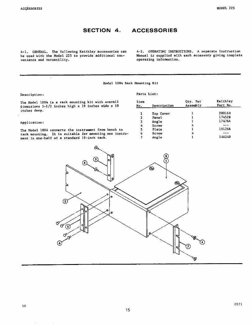
SECTION 4. ACCESSORIES
MorJE?. 225
4-1. GENERAL. The following Keithley accessories can 4-2. OPEBAlmG 1NSTK"CTlONS. A separate InstrUction be used with the Model 225 to provide additional con- Manual is supplied with each accessory giving complete venience and versatility. operating information.
Model 1004 Rack Mounting Kit
Description:
The Model 1004 is a rack mounting kit with overall dimensions 5-l/2 inches high x 19 inches wide x 10 inches deep.
Application:
The Model 1004 converts the instrument from bench to rack mounting. It is suitable for mounting one instru- ment in one-half of a standard 19-inch rack.
Parts Litit:
item Qty. Per Keithley NO. Description Assembly Part NO.
1 Top Cover 1 200168 2 Panel 1 174528 3 Angle 1 17476A 4 screw 4 _-- 5 Plate 1 191266 6 Screw 4 __- 7 Angle 1 146248
10 15
0571
SERVICING MODEL 225
SECTION 5.
5-l. GENERAL. This section contains procedures for checkout and servicing the instrument. Follow the step-by-step procedures for complete servicing.
5-2. SERVICING SCHEDULE. This instrument requires no periodic maintenance beyond the normal care required for high-quality electronic equipment,
5-3. PARTS REPLACEMENT. Refer to the Replaceable Parts List, Section 7, for information regarding corn- ponent specifications and part numbers. Replace corn- ponents as indicated using replacement parts which meet the listed specifications.
SERVICING
5-4. TROUBLESHOOTING.
a. Test Equipment. Refer to Table 5-l for recom- mended test equipment for servicing and calibrating this instrument.
b. Troubleshooting Guide. Refer to Figure 16 for voltages and test points.
NOTE
If the instrument problem cannot be readily located or repaired, contact a Keithley rep- resentative or the Sales Service Department. Cleveland, Ohio.
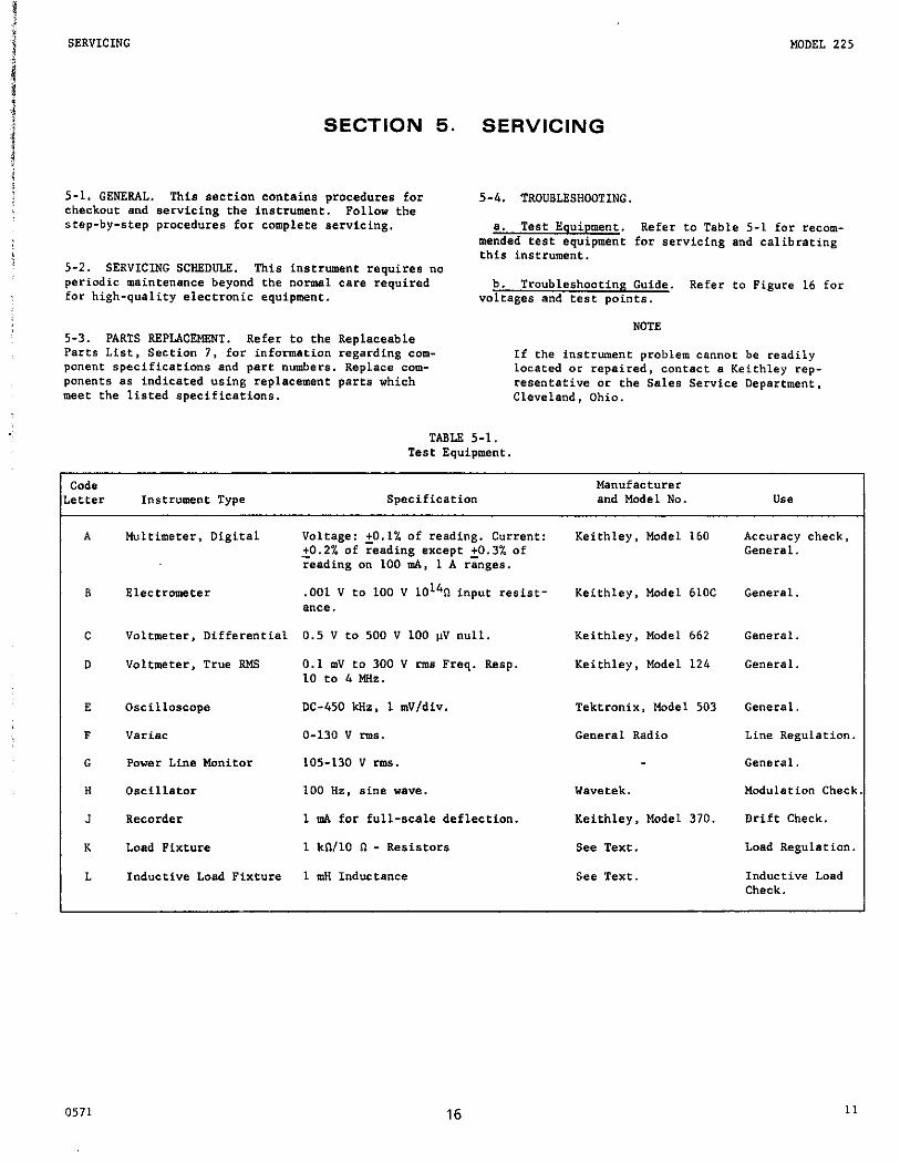
TABLE 5-1. Test Equipment.
Code Manufacturer Letter Instrument Type Specification and Model No. Use
A Multimeter, Digital Voltage: 20.1% of reading. Current: Keithley, Model 160 Accuracy check, 20.2% of reading except 50.3% of General. reading on 100 mA, 1 A ranges.
* Electrometer .OOl V to 100 V lo’“0 input resist- Keithley, Model 610C General. enee
C Voltmeter, Differential 0.5 V to 500 V 100 VV null. Keithley, Model 662 General.
D Voltmeter, True RMS 0.1 mV to 300 V rmm8 Freq. Resp. Keithley, Model 124 General 10 to 4 MHZ.
E Oscilloscope DC-450 kllz, 1 mV/div. Tektronix, Model 503 General
F Variae O-130 ” lms. Genersl Radio Line Regulation.
G Power Line Monitor 105-130 V nos. General
H Oscillator 100 Hz, sine wave. Wavetek. Modulation Check
.I Recorder 1 WA for full-scale deflection. Keithley, Model 370. Drift Check.
K Load Pixture 1 kC/lO 0 - Resistors See Text. Load Regulation.
L Indwtive Load Fixture 1 mH Inductance See Text. Inductive Load Check.
0571 16 11
CALIBRATION
SECTION 6. CALIBRATION
MODEL 225
6-1. GENERAL. This section contains procedures for checking the instrument in order to verify.aperation within specificetions.
6-2. TEST EQUIPMENT. Refer to Table 5-1 for recom- mended test equipment for servicing end calibrating this instrument.
6-3. CALIBRATION PROCEDURE. Refer to Table 6-l far step-by-step procedures for calibrating this instru- ment.
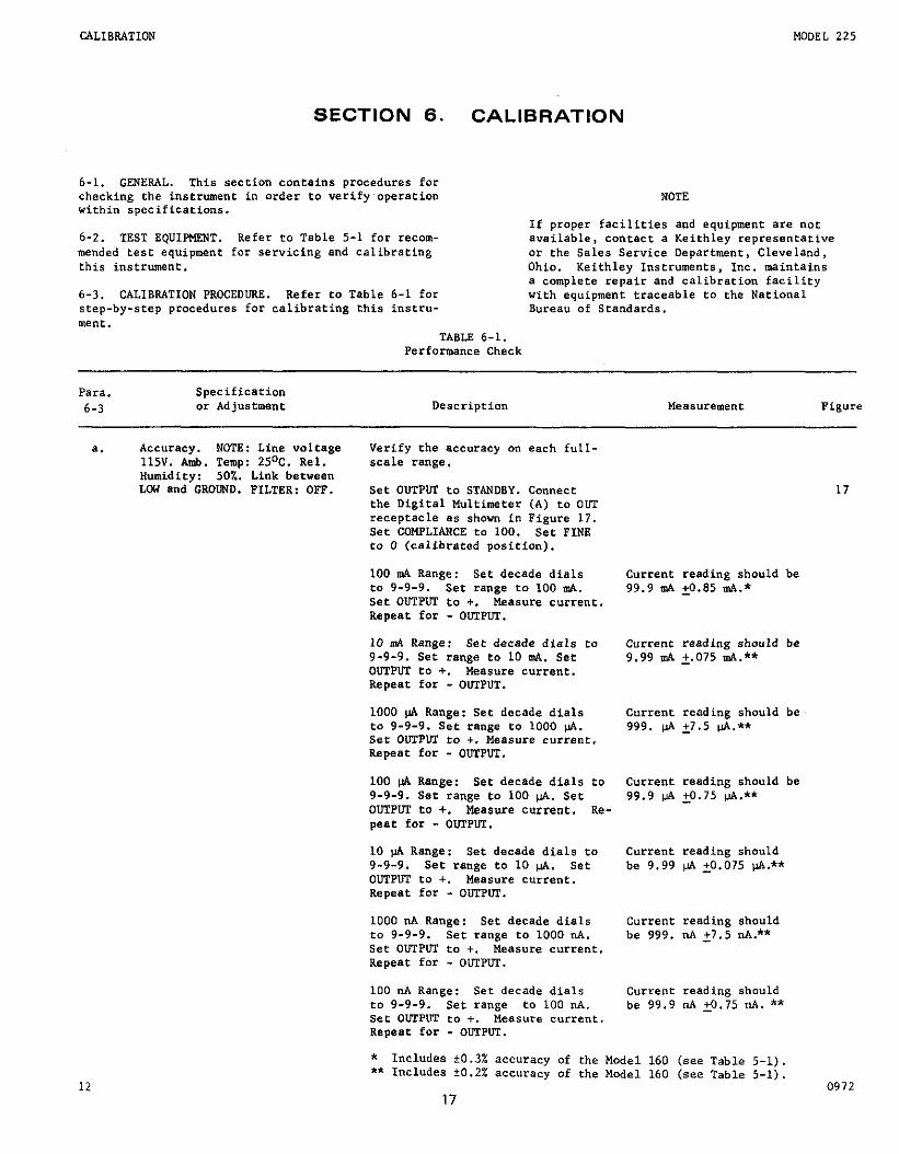
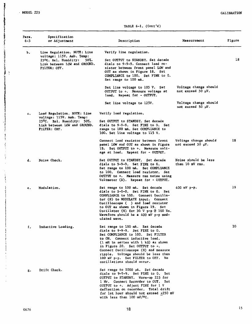
TABLE 6-l. Performance Check
NOTE
If proper facilities end equipment ere not available, contact a Keithley representative or the Sales Service Department, Cleveland, Ohio. Keithley Instruments, Inc. maintains a complete repair end calibration facility with equipment traceable to the National Bureau of Standards.
Par*. Specification 6-3 or Adjustment Description Measurement Figure
a. Accuracy. NOTE: Line voltage Verify the accuracy on each full- 115V. Amb. Temp: 25OC. Rel. scale range. Humidity: 50%. Link between LOW end CROWD. FILTER: OPP. Set OUTPUT to STANDBY. Connect
the Digital Multimeter (A) to OUT receptacle es shown in Figure 17. Set COMPLIANCE to 100. Set FINE to 0 (calibrated position).
100 mA Range: Set decade dials to 9-9-9. Set range to 100 mA. Set OUTPUI to +. Measure current. Repeat for - OUTPUT.
10 18~4 Range: Set decade dials to 9-9-9. Set range to 10 mA. Set OOTPOT to +. Measure current. Repeet for - OUTPUT.
1000 pA Range: Set decade dials to 9-9-9. Set range to 1000 pA. Set OUrPUT to +. Measure current. Repeat for - OUTPUT.
100 pi Range: Set decade dials to 9-9-9. Set range to 100 @.. Set OOTPDT to c. Measure current. Re peat for - ODTPW.
17
Current reading should be 99.9 CA +o.l35 u&4.*
Current reading should be 9.99 EA +.075 !“A.**
Current reading should be 999. “A 27.5 WA.**
Current reading should be 99.9 LLA 20.75 PA.**
12
10 @ Range: Set decade dials to Current reading should 9-9-9. Set range to 10 @. Set be 9.99 fi 20.075 )rA.** OUTPUT to f. Measure current. Repeat for - ODTPW.
1000 nA Range: Set decade dials Current reading should to 9-9-9. Set range to 1000 nA. be 999. nA 27.5 “A.** Set ODTPL’I to +. Measure current. Repeat for - OWIPOT.
100 nA Range: Set decade dials Current reading should to 9-9-9. Set range to 100 “A. be 99.9 nA LO.75 nA. ** Set OLTPUT to +. Measure current. Repeat for - OUTPDT.
* Includes 33.3% accuracy of the Model 160 (see Table 5-I). ** Includes 20.2% accuracy of the Model 160 (see Table 5-l).
17 0972
MODEL 225 CALIBRATION
TABLE 6-1. (Cont'd)
pera. 6-3
Specification or Adjustment Description Measurement
b. Line Regulation. NOTE: Line voltage: 115V. Amb. Temp: 25W. Rel. Humidity: 50%. Link between LOW end GROUND. FILTER: OFF.
C. Lasd Regulation. NOTE: Line voltage: 115". Amb. Temp: 25%. Rel. Humidity: 50%. Link between LOW end GROUND. FILTER: OFF.
d. Noise Check.
e. Modulation.
Inductive Loading.
Drift Check.
0676 18
Verify line regulation.
Set OUIPb"f to STANDBY. Set decade dials to 9-9-9. Connect load re- sistor between front panel Loh( and Om es shown in Figure 18. Set COMPLIANCE to 100. Set FINE to 0. Set renge to 100 mA.
Set line voltage to 105 V. Set 0uT'pvT to +. Measure voltage at load. Repeet for - ODTPDT.
Set line voltage to 125V.
Verify load regulation.
Set ODTPDT to STANDBY. Set decade dials to 9-9-9. Set FINS to 0. Set range to 100 s&i. Set COMPLIANCE to 100. Set line voltage to 115 V.
Connect load resistor between front panel LOW end ODT es shown in Figure 18. Set ODTPUT to l . Measure volt- age et load. Repeat for - OUTPUT.
Set OUl'PuT to STANDBY. Set decade dials to 9-9-9. Set FINE to 0. Set range to 100 mA. Set COMPLIANCE to 100. Connect load resistor. Set ODTPlrr to +. Measure cm* noise using Voltmeter (D). Repeat for - ODTPUT.
Set range to 100 mA. Set decade dials to 5-O-O. Set FINS to 0. Set COMPLIANCE to 100. Connect Oscilla- tor (H) to MODDIATE input. Connect Oscilloscope ( ) end loed resistor to OUT es shown in Figure 19. Set Oscillator (H) for 30 V p-p @ 100 Hz. Waveform should be e 400 mV p-p mcd- ulated "eve.
Set range to 100 mA. Set decede disls to 9-9-9. Set FINE to 0. Set COMPLIANCE to 100. Set FILTER to ON. Connect inductive load. (1 mH in series with 1 kG) es shown in Figure 20. Set OUTPUT to +. Connect Oscilloscope (H) and measure ripple. Voltage should be less than 100 mv p-p. Set FILTER to OFF. No oscillations should occur.
Set range to 1000 PA. Set decade dials to 9-9-9. Set FINS to 0. Set OUTPUI to STANDBY, Warm-up 225 for 1 Hr. Connect Recorder to OUT. Set OUTPUT to +. Adjust FINE for 1 V deflection on recorder. Total drift for 1st hour should not exceed 2250 mV with less then 100 mV/W.
18
Voltage change should not exceed 50 pV.
Voltage change should not exceed 50 uV.
Voltage change should not exceed 50 WV.
18
Noise should be less then 10 m" rms.
400 mv p-p. 19
20
15
CALIBRATION
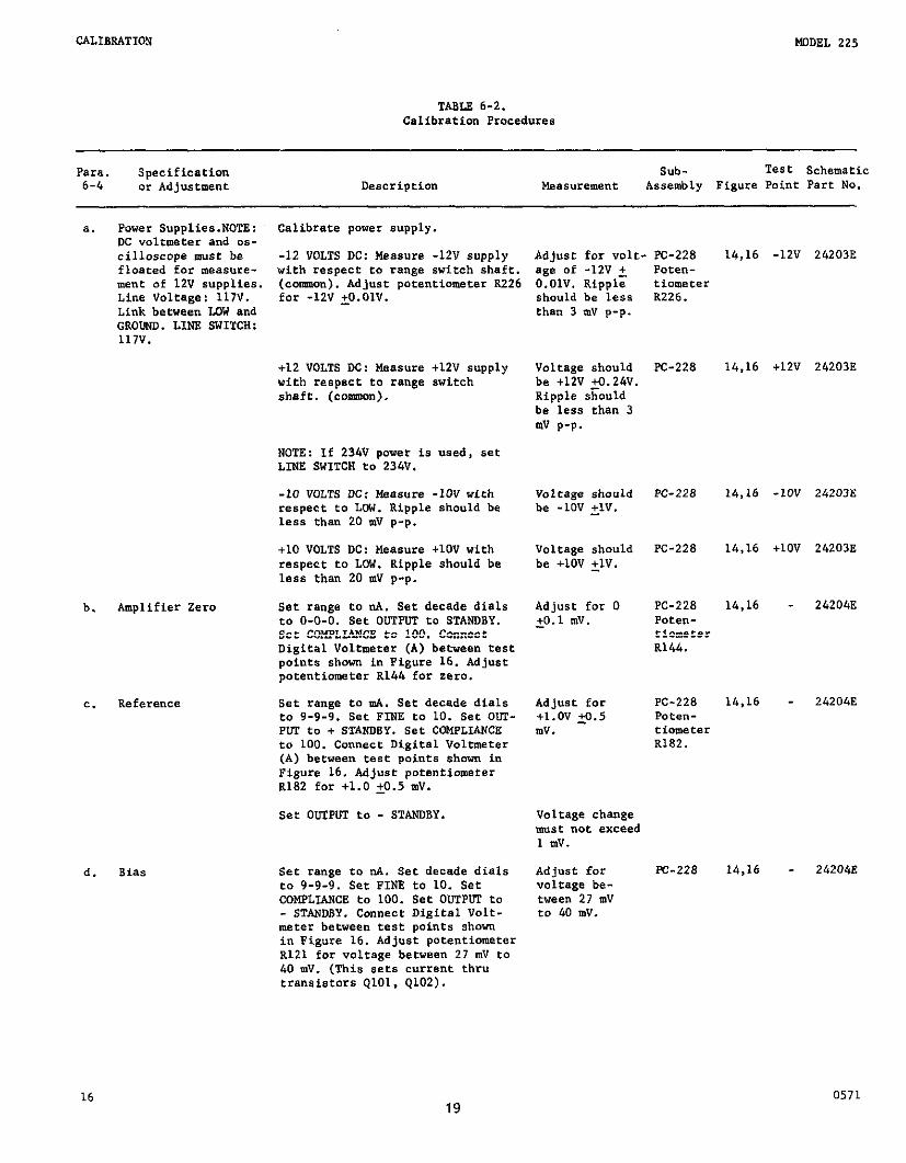
TABLE 6-2, Calibration Procedures
MODEL 225
Para. Specification Sub- Test Schematic 6-4 or Adjustment Description Me~S”r~tlEtlt Assembly Figure Point Part No.
a.
b.
e.
Power Supplies.NOTE: DC voltmeter and os- cilloscope must be floated for measure- ment of 12v supplies. Line Voltage: 117v. Link between LOW and CRODND. LINE SWITCH: 117v.
Amplifier Zero
Reference
d. Bias
Calibrate power supply.
-12 VOLTS DC: Measure -12V supply with respect to range switch shaft. (cnmnon). Adjust pcaentlometer B226 for -17.v +o.o1v.
+12 VOLTS DC: Measure +lZV supply with respect to range switch shaft, (common).
NOTE: If 234V power 1s used, set LINE SWITCH to 234V.
-10 VOLTS DC: Measure -lOV with respect to LOW. Ripple should be less than 20 mV p-p.
+lO VOLTS DC: Measure +lOV with respect to LOW. Ripple should be less than 20 SIV p-p.
Set range to nA. Set decade dials to O-O-O. Set OUTPUT to STANDBY. set COMPLIANCE to 100. COnnecc Digital Voltmeter (A) between test points shown in Figure 16. Adjust potentiometer R144 for zero.
Set range to mA. Set decade dials to 9-9-9. Set FINE to 10. Set OUT- PUT to + STANDBY. set COMPLIANCE to 100. connect Digital Voltmeter (A) between test points ehown in Figure 16. Adjust potentiometer R182 for +1.0 LO.5 mv.
Set OIJCPCT to - STANDBY.
Set rsn~e to nA. Set decade dials to 9-9-G. Set FINE to 10. Set COMPLIANCE to 100. Set OUTFliT to - STANDBY. Connect Digital Volt- meter between test points shown in Figure 16. Adjust potentiometer X121 for voltage between 27 mV to 40 mV. (This sets current thru transistors QlOl, Q102).
Ad~just for volt- PC-228 ag; of -12v + O.OlV. Ripple should be less than 3 mV p-p.
Voltage should be +12V +o.ZW. Ripple should be less than 3 mv p-p.
Voltage should be -lOV +lV.
Voltage should be +lOV +‘V.
Adjust for 0 20.1 mv.
Adjust for +,.ov 20.5 SIV.
Voltage change must not exceed 1 mv.
Adjust for voltaSe be- tween 27 mV to 40 mv.
poten- tiometer R226.
PC-228
PC-228
PC-228
PC-228 Poten- riometer R144.
PC-228 Poten- tiometer RlS2.
PC-228
14,16 -12V
14.16 +12V
14316 -lOV
14,16 +lOV
14.16 -
14.16 -
14.16 -
24203E
242038
242032:
24203E
24204E
24204E
242043
16 19
0571
MODEL 225 CALIBRATION
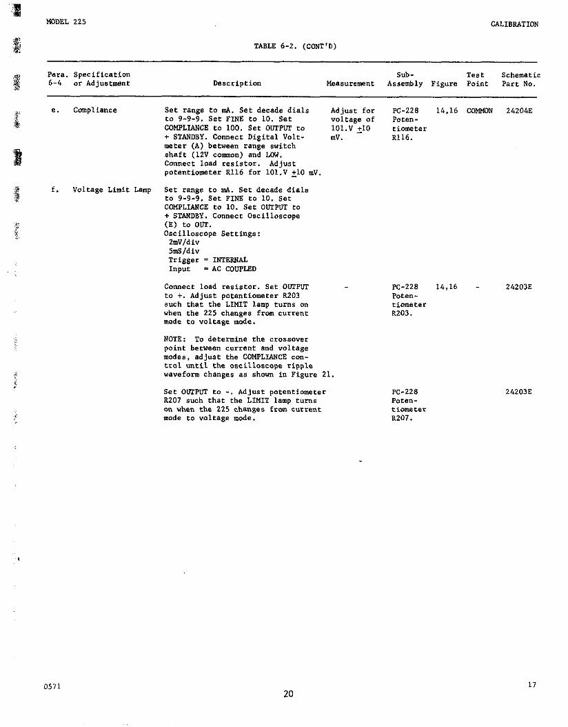
TABLE 6-2. (CONT’D)
Para. Specification 6-4 or Adjustment Description
Sub- Test Schematic Measurement Assembly Figure Point Part No.
Compliance
Voltage Limit Lamp
Set range to mA. Set decade dials Adjust for PC-228 14,16 COMNON 24204E to 9-9-9. Set FINE to 10. Set voltage Of potan- COMPLIANCE to 100. Set OUTPm to 1Ol.V +10 tiorseter + STANDBY. Connect Digital Volt- mV. R116. meter (A) between range switch shaft (12V eonrmon) and LOW. Connect load resistor. Adjust potentiometer R116 for 1Ol.V +lO mv.
Set range to mA. Set decade dials to 9-9-9. set FINE to 10. set COMPLIANCE to 10. Set OUTPUT to + STANDBY. Connect Oscilloscope (E) to OUT. Oscilloscope settings:
2mVldiv SmS/div Trigger = INTERNAL Input = AC COWLED
Connect load resistor. Set OUTPW to +. Adjust potentiometer R203 such that the LIMIT lamp turns an when the 225 changes from current mode to voltage mode.
PC-228 14,16 - 24203E Poten- tiometer R203.
NOTE: To determine the crowover point between current and voltage modes, adjust the COMPLIANCE con- trol until the oscilloscope ripple waveform changes as shown in Figure 21.
Set OUTPCT to -. Adjust potentiometer PC-228 R207 such that the LIMIT lamp turns Poten- on when the 225 changes from current tiometer mode to voltage mode. R207.
24203E
0571 20
17
i
CALIBRATION MODEL 225 -
FIGURE 17. Accuracy Check FIGURE 18. Regulation Check
I ~- I
I LLOSCOPE OSCILLOScOPE
MILLATOR osc
XIVPP ‘L 225 OUT 0
OUTPUT 225
IOOHz ?A00
IS 40% OF F.S. &J-P)
OUTFUT <ImnY PP
m A 07 m
FIGURE 19. Modulation Check FIGURE 20. Inductive Load Check
FIGURE 21. Current Mode Vs Voltage Mode Waveforms
18 21 0676
MODEL 225
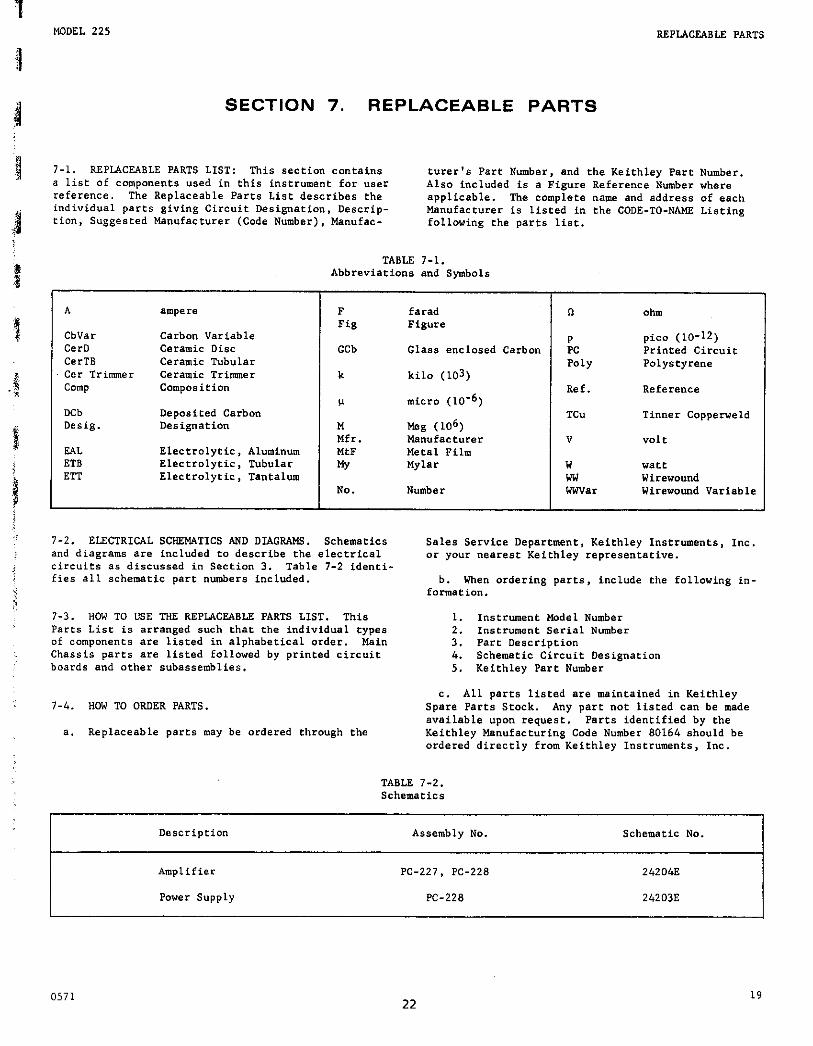
SECTION 7. REPLACEABLE PARTS
KKPLACKAStE PARTS
7-l. REPLACEABLE PARTS LIST: This section contains a list of components used in this instrument for user reference. The Replaceable Parts List describes the
turer.‘s Part Number, and the Keithley Part Number. Also included is a Figure Reference Number where applicable.
individual parts giving Circuit Designaticn, Descrip- The complete name and address of each
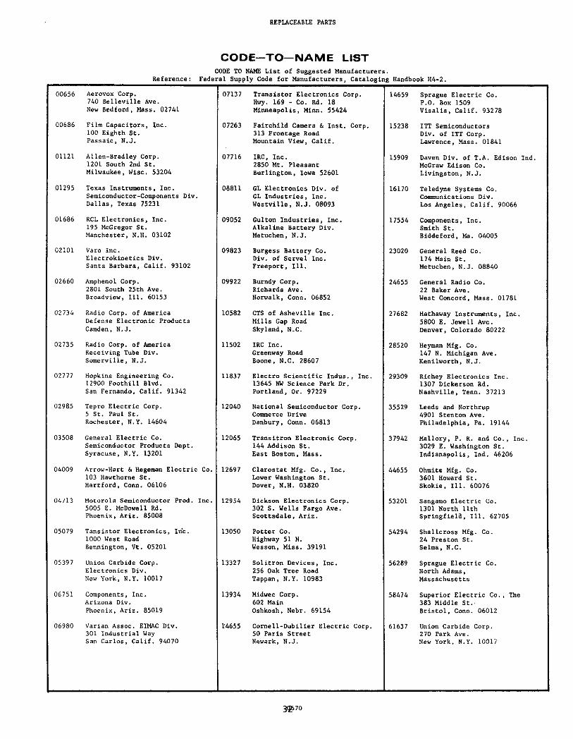
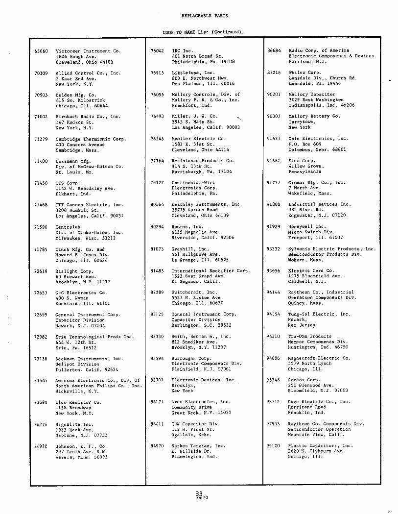
tion, Suggested Manufacturer (Code Number), Manufac- Manufacturer is listed in the CODE-TO-NAME Listing following the parts list.
A ampere
CbVar Carbon Variable CerD Ceramic Disc CerTB Ceramic Tubular Cer Trimmer Ceramic Trimmer Camp Composition
DCb Deposited Carbon Desig. Designation
F.AL Electrolytic, Aluminum ETB Electrolytic, Tubular ETI Electrolytic, Tantalum
TABLE 7-l. Abbreviations and symbols
F farad Fig Figure
GCb Glass enclosed Carbon
k kilo (103)
!-I micro (10-6)
M Meg (10% Mfr. Manufacturer MtF Metal Film MY Mylar
NO. Number
0 ohm
FC pica (10-12) Printed Circuit
Paly Polystyrene
Ref. Reference
TC” Tinner COpperweld
V VOlL
” watt mi Wirewound War Wirewound Variable
7-2. ELECTRICAL SCHEMATICS AND DIAGRAMS. Schematics Sales Service Department, KeithLey Instruments, Inc. and diagrams are included to describe the electrical or your nearest Keithley representative. circuits ss discussed in Section 3. Table 7-2 ldenti- fies all schematic part numbers included. b. When ordering parts, include the following in-
formation.
7-3. HOW TO USE THE REPLACEABLE PARTS LIST. This Parts List is arranged such that the individual types of camponencs are Listed in alphabetical order. Main Chassis parts are listed followed by printed circuit boards and other subassemblies.
1. Instrument Model Number 2. Instrument Serial Number 3. Part Description 4. Schematic Circuit Designatian 5. Keithley Part Number
7-4. HOW TO ORDER PARTS.
a. Replaceable parts may be ordered through the
c. All parts listed are maintained in Keithley Spare Parts Stock. Any part not listed can be made available upon request. Parts identified by the Keithley Manufacturing Code Number 80164 should be ordered directly fram Keithley Instruments, Inc.
TABLE 7-2. Schematics
Description Assembly No. Schematic No.
Amplifier
Power Supply
PC-227, PC-228
PC-228
242048
24203E
0571 22 19
REPlACEABu3 PARTS
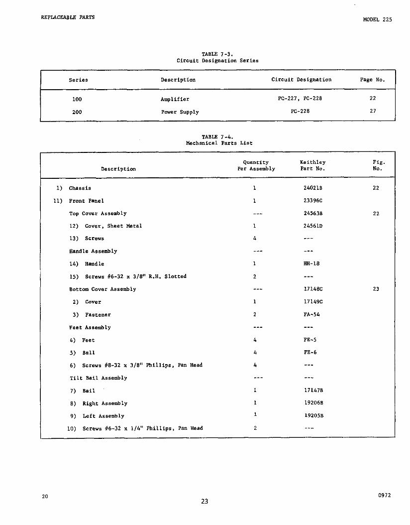
TABLE l-3. Cfrcult Designation series
MODEL 225
series Description
100 Amplifier
200 Power supply
Circuit Designation
PC-227, PC-228
PC-228
Page No.
22
27
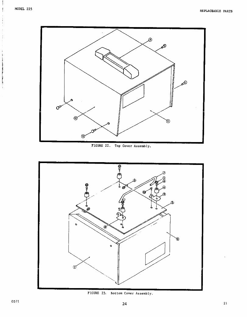
TABLE 7-4. Mechanical Parts List
Quantity K.Sithley Fig. De*CdptiD” Per Assembly Fart No. NO.
1) Chassis 1 240218 22
11) Front Panel 1 2339%
Top Cover Assembly --- 245630 22
12) Cover, Sheet Metal 1 24561D
13) screws 4 _--
Handle Assembly _-- __-
14) Handle 1 m-18
15) Screws 86-32 x 3/S” R.H. Slotted 2 _--
Bottom Cover Assembly --- 17148C 23
2) cover 1 17149c
3) Fastener 2 FA-54
Feet Assembly -_- ---
4) Feet 4 FE-5
5) Ball 4 FE-6
6) Screws OS-32 x 3/S” Phillips, Pan Head 4 --_
Tilt Bail Assembly _-- ---
7) Bail 1 171478
8) Right Assembly 1 192068
9) left Assembly 1 19205B
10) Screws 06-32 x l/4” Phillips, Pan Head 2 ---
20 23
0972
MODEL 225 REPlACEABLE PARTS
FIGURE 22. Top Cover Assembly.
0571
Botkm Cover Assembly.
24 21
REPLACEABLE PARTS MODEL 225
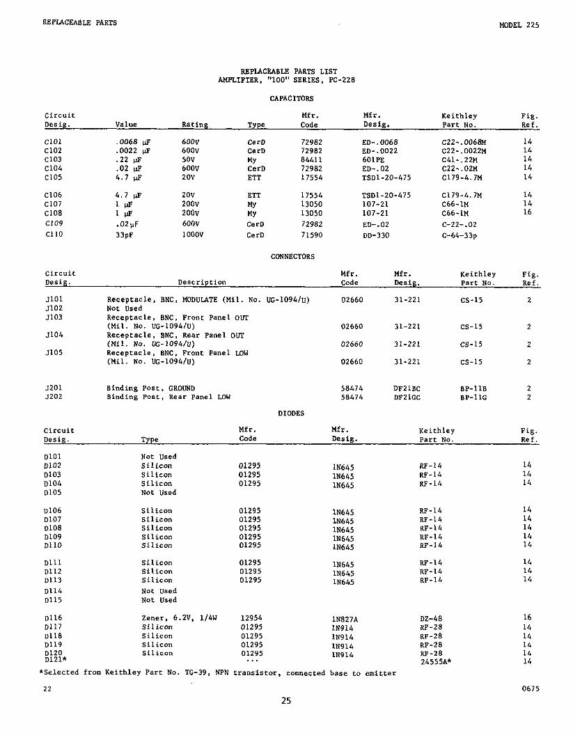
REPIACEABLE PARTS LIST AMPLIFIER, “100” SERIES, PC-228
CAPACITORS
CiCC”if Desig.
Cl01 Cl02 Cl03 Cl04 Cl05
Cl06 Cl07 cl08 Cl09 Cl10
Value Raring
.0068 fl 6OOV
.0022 p 600~
.22 &dJ 501)
.02 $2 600~ 4.7 pF 2ov
4.7 @ 2ov lllF zoov lP 2oov .OZuF 600” 33PF 1ooov
Mfr. Mfr. Keithley Fig. Type Code Desig. Part No. Ref.
&L-D 72982 ED-.0068 C22-.006SM 14 CerD 72982 ED-.0022 C22-.0022M 14 MY 84411 601PE C61-.22M 14 CerD 72982 ED-.02 C22-.02M 14 ETT 17556 TSDl-20-475 C179-4.7M 14
ETT 17554 TSDl-20-475 C17Y-4.7M 14 MY 13050 107-21 C66-1M 14 MY 13050 107-21 C66-1M 16 CerD 72982 ED-.02 c-22-.02 CerD 71590 DD-330 C-64-33~
CONNECTORS
Cik-C”it Desig. Description
Mfr. Mfr. Code Desig.
Keithley Fig. Part No. Ref.
3101 Receptacle, BNC, MODUuTE (Mil. NO. UG-1094/u) 02660 31-221 cs-15 2 5102 Not Used 3103 Receptacle, BNC, Front Panel om
(Mil. No. W-1096/U) 02660 31-221 cs-15 2 5106 Receptacle, BNC, Rear Panel OLPP
(nil. ii*. UG-1094kl) 02660 31-221 cs-15 2 J105 Receptacle, SNC, Front Panel LOW
(Mil. No. UG-1094/U) 02660 31-221 cs-15 2
J201 Binding Post, GROUND 58474 DF21BC BP-118 2 5202 Binding Post, Rear Panel LOW 58474 DF21GC BP-11G 2
DIODES
Circuit Desig. Type
Mfr. Mfr. Keithley Fig. Code Desig. Parr NO. Ref.
DlOl 0102 D103 D104 D105
0106 0107 0108 D109 DllO
Dill 0112 D113 0114 D115
0116 D117 0118 Ill19 D120 n121*
Not Used Silicon Silicon Silicon Not Used
01295 lN645 RF-14 01295 lN645 RF-14 01295 lN645 RF-14
s11icon 01295 lN645 RF-14 Silicon 01295 lN645 RF-16 Silicon 01295 lN645 RF-14 Silicon 01295 lN645 RF-14 Silicon 01295 lN645 RF-14
Silicon Silicon Silicon Not Used Not Used
01295 18645 RF-14 01295 lN665 RF-14 01295 lN645 RF-l&
Zener, 6.2V, 1/6W Si 1 icon Silicon Silicon Silicon
12956 01295 01295 01295 01295
. . .
lN827A lN916 lN914 lN914 lNY14
DZ-68 RF-28 RF-28 RF-28 RF-28 26555A*
*Selected from Keithley Part No. TG-39, NPN transistor, connected base to emitter
22 25
14 14 14
14 14 14 14 14
14 14 14
16 14 14 14 14 14
0675
MODEL 225 RRPIACFABLE PARTS
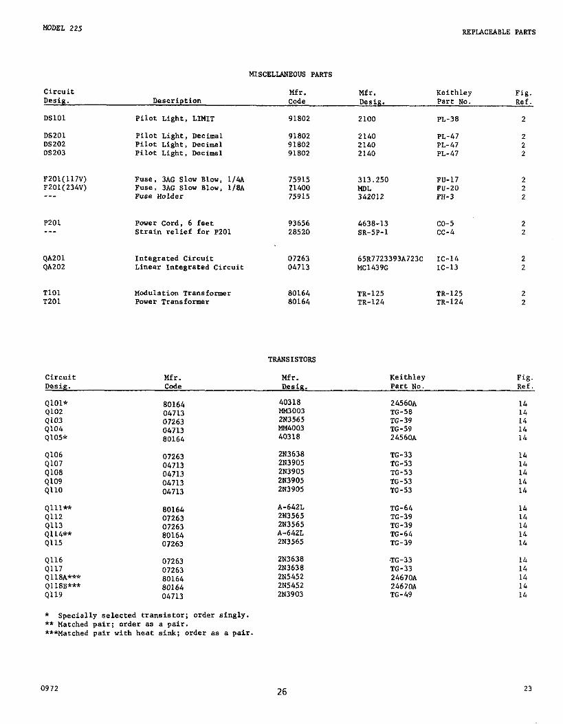
MISCELIANEOUS PARTS
Circuit Desig. Description
Mfr. Mfr. Keithley Fig. Code Desk. Part No. Ref.
DSlOl
DS201 DS202 OS203
FZOl(117V) FZOl(236V)
P201 Power Cord, 6 feet 93656 4638-13 _-_ Strain relief for P201 28520 SR-SP-1
QA201 Integrated Circuit 07263 65R7723393A723C QA202 Linear Integrated Circuit 04713 MCl639G
TlOl Modulation Transformer 80164 TR-125 T201 Power Transformer 80164 TR-124
Pilot Light, LIMIT 91802 2100
Pilot Light, Decimal 91802 2140 Pilot Light, Decimal 91802 2140 Pilot Light, Decimal 91802 2160
Fuse, 3AG slow Blow, 1/4A 75915 313.250 Fuse, 3AG slow Slow, 1/8A /1600 MDL Fuse Holder 75915 342012
PL-38 2
PL-47 2 PL-47 2 PL-47 2
FU-17 2 FU-20 2 FH-3 2
co-5 2 cc-4 2
IC-14 2 IC-13 2
TR-125 2 TR-124 2
TRANSISTORS
circuit Mfr. Mfr. Keithley Fig. Desig. Code Desig. Part No. Ref.
80164 04713
9103 07263 Q106 04713 Q105* 80164
Q106 07263 Q107 04713 QlO8 04713 Q109 04713 QllO 04713
Qlll** 80164 Q112 07263 Q113 07263 Q114** 80164 Q115 07263
Q116 07263 Q117 07263 QllSA*** 80164 QllsB*** 80164 Q119 04713
* Specially selected transistor: order singly. ** Matched pair; order as a pair. ***Matched pair with heat sink; order as a pair.
40318 MM3003 2N3565 MM6003 40318
2133638 2N3905 283905 2N3905 2N3905
A-642L 2N3565 2N3565 A-642L 2N3565
2N3638 2N3638 2N5652 2N5452 2N3903
2456011 TG-58 TG-39 TG-59 26560A
TG-33 TG-53 TG-53 TG-53 TG-53
TG-64 TG-39 TG-39 TG-64 TG-39
,TG-33 TG-33 24670~ 24671X TG-49
14 14 14 14 16
14 14 14 14 14
14 14 14 14 14
14 14 14 14 14
0972 26 23
REPlACEABLE PARTS MODEL 225
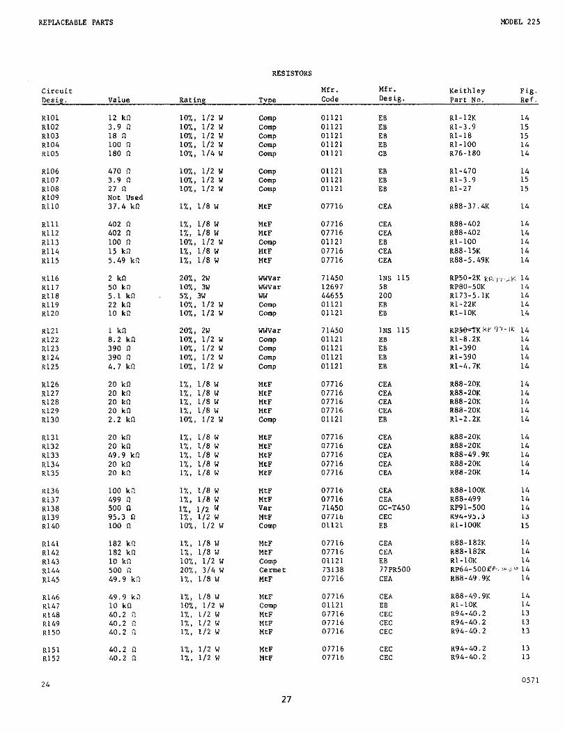
RESISTORS
circuit Oesig. Value Rating Type
Mfr. Mfr. Keithley Fig. Code Des&. Part NO. Ref.
RIO1 12 k* RI02 3.9 n R103 18 R RI04 100 n RIO5 180 n
IO%, l/2 w 10%. l/2 w 10%, l/2 w 10%, l/2 w lO%, l/4 w
camp camp camp camp comp
01121 01121 01121 01121 01121
RlO6 RI07 RI08 R109 RllO
470 n 3.9 n 27 R Not USed 37.4 k0
lO%, l/2 w lO%, l/2 " lO%, l/2 "
camp camp camp
01121 01121 01121
l%, l/8 W MtF 07716
Rlll 402 c-t I%, l/8 W MeF 07716 R112 402 !-I l%, l/8 W MCF 07716 R113 100 R lO%, l/2 w camp 01121 Rl14 15 kil I%, 1/a w MtF 07716 Rl15 5.49 k0 l%, l/8 w MCF 07716
~116 RI17 Rl18 Rll9 RI20
2 k0 50 kn 5.1 kfl 22 k0 10 kR
R121 R122 R123 R124 R125
20%, 2w 10%. 3w 5%, 3w 10%, l/2 w IO%, l/2 w
20%, 2w lO%, l/2 W IO%, l/2 w lO%, l/2 w IO%, l/2 w
1%. l/8 w 1%; l/8 w I%, l/8 W I%, l/8 W IO%, l/2 W
WWVX 71450 WW"ar 12697 ww 44655 camp 01121 camp 01121
1 kIl 8.2 k0 390 n 390 n 4.7 kfl
wwvar camp camp camp camp
71450 01121 01121 01121 01121
R126 R127 RI28 R129 R130
20 kQ 20 kn 20 kR 20 k0 2.2 kR
MfF 07716 MtF 07716 MtF 07716 MtF 07716 camp 01121
Rl31 20 kR l%, l/8 W MtF 07716 R132 20 kn 1%, l/8 W MW 07716 R133 49.9 ks-, l%, l/8 W MY3 07716 R134 20 kQ l%, l/8 W MtF 07716 RL35 20 kR l%, l/8 W MCF 07716
~136 100 kl? l%, l/8 W MtF 07716 R137 499 n 1%, l/8 w ?-RF 07716 R138 500 n l%, l/2 W "ar 71450 R139 95.3 n l%, I/2 w MtF 07716 R140 100 n lo%, l/2 w camp 01121
R141 R142 R143 RI44 R145
182 k0 182 kR 10 kn 500 0 49.9 kt?
l%, 1/a w l%, l/8 w lo%, l/2 w 20%, 314 w l%, 1/a w
I%, l/8 w lO%, l/2 w l%, 1/z w l%, l/2 " l%, l/2 W
l%, l/2 w I%, l/Z w
MtF 07716 MtF 07716 Camp 01121 cermee 73138 MtF 07716
RI46 R147 RI48 R149 R150
49.9 kfi 10 kR 40.2 0 40.2 i? 40.2 0
07716 01121 07716 07716 07716
Rl51 RI52
24
40.2 R 40.2 0
MfF COUIP MCF MfF MeF
MtF me
27
07716 CRC 07716 CEC
88 EB EB ER cs
E8 RR EB
CEA
CEA CEA E8 CEA CEA
INS 115 58 200 EB EL3
1NS 115 EB EB ES RR
CEA CEA CEA CEA EE
CEA CEA CEA cl?* CEA
CEA CEA GC-T450 CRC ES
CEA CEA E8 77PR500 CEA
a.4 R88-49.9K 14 ES RL-1OK 14 CEC R94-40.2 13 CRC CEC
Rl-12K 14 RI-3.9 15 RI-18 15 Rl-100 14 R76-180 14
RI-470 14 RI-3.9 15 RI-27 15
R88-37.4K 14
R88-402 14 R88-402 14 RI-100 14 R88-15K 14 R88-5.49K 14
RP50-2K @.,,~,~'K 14 RP80-50K 14 Rl73-5.lK 14 Rl-22K 14 RI-1OK 14
Rp!&=TKw1'-il: 14 RI-8.2K 14 RI-390 14 Rl-390 14 RI-4.7K 14
R88-20K 14 R88-20K 14 R88-20K 14 R88-20K 14 Rl-2.2K 14
R88-20K 14 R88-20K 14 R88-49.9K 14 R88-20K 14 R88-20K 14
R88-LOOK 14 R88-499 14 RP91-500 14 R94-95.3 13 RI-1OOK 15
R88-182K 14 R88-182K 14 Rl-LOK 14 RP64-500PP.!1?~." 14 R88-49.9K 14
R94-40.2 13 R94-40.2 13
R94-40.2 13 894-40.2 13
0571
MODEL 225 REPLACEABLE PART’S
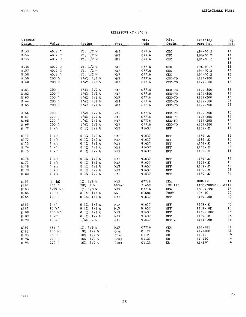
RESISTORS (Conc’d.)
circuit Oesig. Rating TYPe
Mfr. Mfr. Code oesig.
Keichley Fig. Part NO. Ref.
RL53 40.2 ? Rl54 40.2 1 R155 40.2 :
RI56 R157 Rl58 Ri59 Rib0
40.2 :! 40.2 0 40. 2 ‘5 200 2 200 :I
RI61 RI62 Rl63 RI64 R165
200 ? 200 I 200 ? 200 : 200 1
RI66 RI67 RI68 Rib9 Rl70
200 ‘1 200 ,2 200 ? 200 ‘2 1 k-i
Kiil Rii? RI73 R174 R175
1 k,? 1 k.1 1 k’l 1 kl 1 kl
RI76 KL77 8178 K179 Ri80
1 k.! 1 k.3 , k(l 1 k:! 1 k!-l
11181 K182 Rl83 R184 RI85
1 kn 200 2 4.99 kn 10 R 100 2
RI86 R187 Rl88 R189 Ii190
I k:! 10 k? 100 k? 1 w: 10 M:l
RI91 RI92 RI93 RI94 Ri95
681 3 100 k:! 10 ,) 220 > 220 :?
I%, l/2 w I%, l/2” I%, l/2 w
l%, l/2 w l%, l/2 w 1%. 112 w l/4%, 1/z W l/4%, 112 W
l/4’/., l/2 w 1/a, l/2 w l/4%, 112 w l/4%, l/2 w l/4%, L/2 w
l/4%, l/2 w l/4%, l/2 w l/4%. l/2 w l/4%, 1/z w O.l%, l/2 w
O.l%, l/2 w O.l%, 112 w O.l%, l/2 w O.l%, l/2 w O.l%, l/2 w
O.l%, l/2 W O.l%, l/2 W o.l%, L/2 w O.l%, l/2 w O.l%, l/2 w
l%, l/8 W 20%, 2 w l%, l/8 W O.l%, l/4 w O.l%, l/2 w
0.1%. l/2 w O.l%, 1/z W O.l%, l/2 w O.l%, 112 w 114%. 2 w
1%. l/8 W lo%, l/2 w lO%, l/2 w lo%, l/2 w lo%, l/2 W
MtF 07716 CEC R94-40.2 MtF 07716 CEC R94-40.2 MtF 07716 CEC R94-40.2
MtF l-lee MfF MtF MtF
MtF MtF MtF MtF MfF
MtF MCF MCF MtF MtF
MW MW MtF MW MtF
MtF lee MtF MtF MfF
MtF ww”a r MtF ww MLF
MtF MtF MCF MtF MCF
07716 CEC R94-40.2 07716 CEC R94-40.2 07716 CEC R94-40.2 07716 CEC-TO Rl27-200 07716 CRC-TO R127-200
07716 CEC-TO RL27-200 07716 CEC-TO KL27-200 07716 CEC-TO R127-200 07716 CEC-TO R127-200 07716 CEC-TO Rl27-200
07716 CEC-TO 07716 CEC-TO 07716 CRC-TO 07716 CEC-TO 91637 MFF
RL27-200 R127-200 R127-200 R127-200 Rl69-1K
91637 MFF R169-IK 91637 MFF R169-1K 91637 MFF Rl69-lK 91637 MFF Rl69-lK 91637 MTF RL69-1K
91637 MFF R169-1K 91637 MFF R169-1K 91637 Mm R169-1K 9,637 Mm R169-lK 91637 MFF Rl69-1K
07716 CEA 71450 INS 115 07716 CEA 01686 7009 91637 MTF
R88-lk 14 RP50-200RP.iG'+i)o 14 R88-4.99K 14 R95-10 15 Rl69-100 15
91637 MFF R169-1K 15 91637 MFF Rl69-1OK 15 91637 MFF R169-100K 15 91637 MFF Rl69-lM 15 91637 MIT-2 RL61-1OM 15
13 13 13 13 13 13 13 13 13
13 13 13 13 13
13 13 13 13 13
13 13 13 13 13
L3 13 13 13 13
07716 CEA R88-681 16 01121 EL3 RI-100K 16 01121 EB ill-10 16 01121 EB RI-220 14 01121 E8 KL-220 14
0774 25
28
REPLACEABLE PARTS MODEL 225
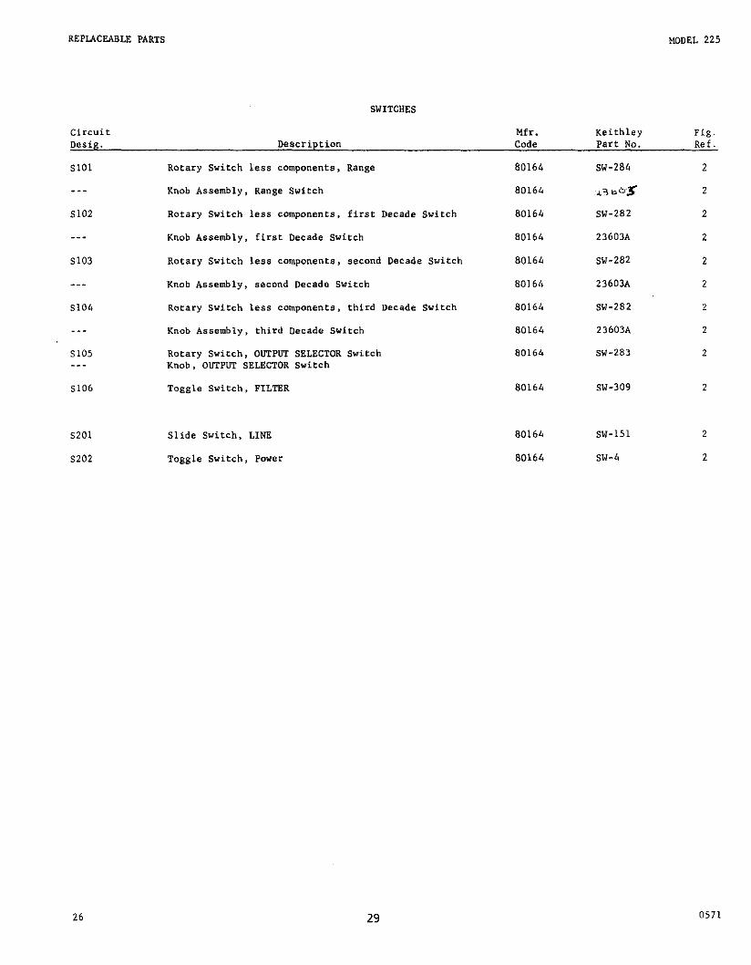
SWITCHES
circuit Desig. Description
Mfr. Code
Keithley ear-t No.
Fig. Ref.
SlOl
---
5102
___
s103
__-
SlO4
_-_
SlO5 ---
5106
Rotary Switch less components, Range
Knob Assembly, Range Switch
Rotary Switch less components, first Decade Switch
Knob Assembly, first Decade Switch
Rotary Switch less components, second Decade Switch
Knob Assembly, second Decade Switch
Rotary Switch less components, third Decade Switch
Knob Assembly, third Decade Switch
Rotary Swifch, DDTPDT SELECTOR Switch Knob, OUTPUT SELECTOR Switch
Toggle Switch, FILTBR
80164 SW-284
80164 23 bti3
80164 SW-282
80164 2360311
80164 SW-282
80164 23603.4
80164 SW-282
80164 23603A
80164 SW-283
80164 SW-309
5201 Slide Switch, LINE 8016L SW-151 2
s202 Toggle Switch, Power 80164 SW-4 2
26 23 0571
MODEL 225 REPlACEABLE PARTS
POWER SUPPLY, "200 SERIES
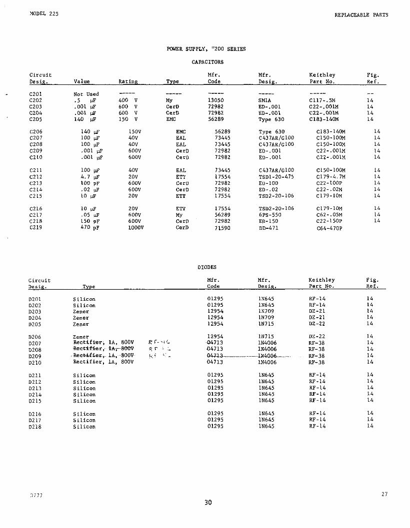
CAPACITORS
Circuit Desig. Value Rating Type
Mfr. Code
Mfr. Desig.
Keithley Part No.
Fig. Ref.
C201 c202 C203 C204 C205
Not Used .5 P .OOl !AF .OOl pF 140 NF
_---- -____ 400 " 600 " 600 " 150 "
_--_- MY CerD CWD EMC
13050 72982 72982 56289
SMl.4 ED-.001 ED-.001 Type 630
C206 140 p 15ov EMC 56289 Type 630 C207 100 &IF 4ov EAL 73445 C437ARfGlOO C208 100 p 4ov SAL 73445 C437ARfGlDO C209 ,001 g 600" CerD 72982 ED-.001 c210 ,001 fl 600V cero 72982 ED-.001
C211 c212 C213 c214 C215
100 pF 4.7 &J 100 PF .02 pF 10 w
4ov zov 600" 600" 2ov
EAL ETT CerD cerD ETT
73445 17554 72982 72982 17554
C437ARfGlOO TSDl-20-475 ED-100 ED-.02 TSD2-20-106
C216 10 IrF 2ov ET-r 17554 TSDZ-20-106 c217 .05 p 600" MY 56289 6PS-550 C218 150 pF 600~ &k-D 72982 ED-150 C219 470 pF 1ooov tern 71590 DD-471
----- -- Cll7-.5M 14 C22-.OOlM 14 czz-.OOlM 14 Cl83-14OM 14
C183-140M 14 Cl50-1OOM 14 c150-IOOM 14 c22-.OOlM 14 c22- .OOlM 14
Cl50-100M 14 Cl79-4.7M c22-LOOP C22-.02M c179-low
C179-10M C62-.05M C22-150P C64-470P
14 14 14 14
14 14 14
DIODES
Mfr. Mfr. Keiehley Fig. Code DesiF,. Part No. Ref.
0201 0202 0203 0204 D205
D206 0207 0208 D209 D210
zener Rectifier, IA, 800V uectifier,~ -fit,-8mv
-ReeEGieer,. lA,~-800V Rectifier, 1.4, 800V
0211 Silicon D212 Silicon 0213 Silicon 0214 Silicon 0215 Silicon
D216 Silicon Silicon Silicon
D217 D218
01295 lN645 RF-14 01295 lN645 RF-14 12954 lN709 DZ-21 12954 IN709 DZ-21 12954 IN715 DZ-22
12954 ~04713 04713 04&&L 04713
01295 01295 01295 01295 01295
01295 01295 01295
lN715 lN4006 lN4006
-----B14006-- IN4006
lN645 lN645 IN645 lN645 lN645
lN645 113645 lN645
DZ-22 RF-38 RF-38 RF-38 RF-38
RF-14 RF-14 RF-14 RF-14 RF-14
RF-14 RF-14 RF-14
14 14 14 14 14
14 14 14 14 14
14 14 14 14 14
14 14 14
0777 27 30
REPlACEmLE PARTS MODEL 225
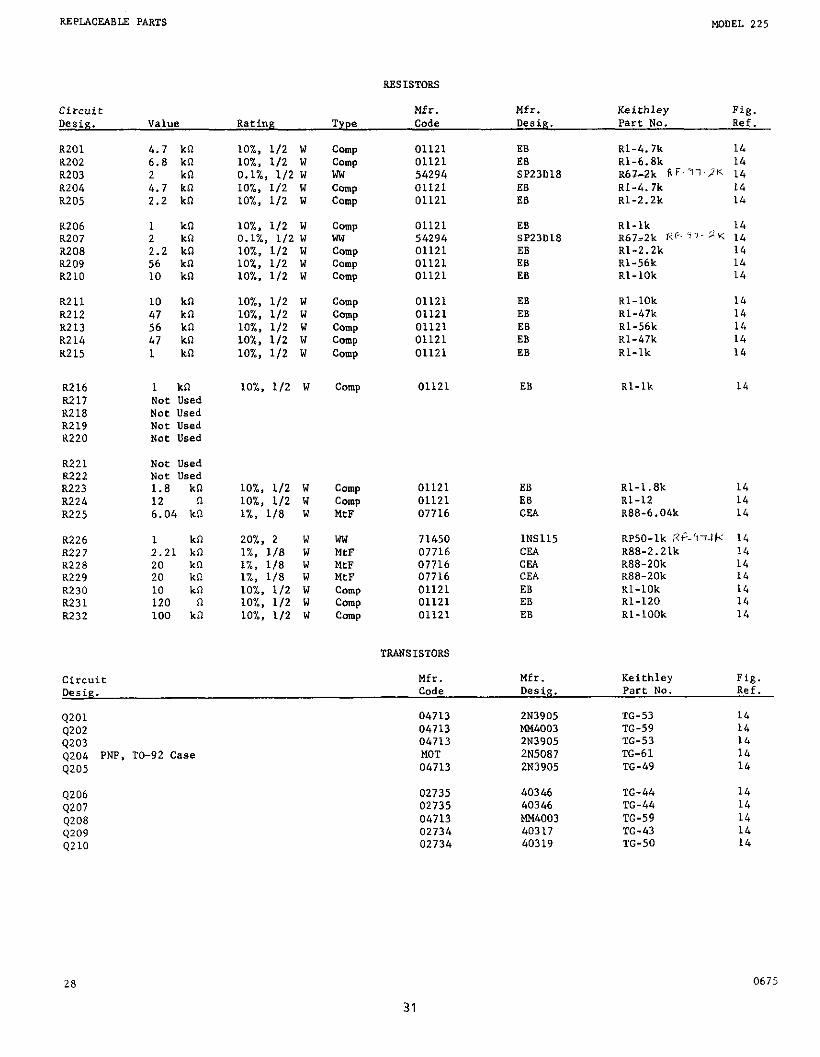
Circuit Desig. Value Rating Type
Mfr. Mfr. Keithley Fig. Code llesig. Pare NO. Ref.
R201 4.7 kR R202 6.8 kR R203 2 kfi R204 4.7 k0 R205 2.2 k0
R206 R207 RZOS R209 R210
1 k0 2 kn 2.2 kft 56 kfl 10 kfl
It211 R212 R213 R214 R215
10 kfl 47 kfl 56 ktl 47 kC 1 kn
R216 R217 R218 R219 R220
1 kC Not Used Not Used Not Used Not Used
R221 R222 8223 R224 R225
Not Used Not Used 1.8 kfl 12 n 6.04 k0
R226 R227 R228 R229 R230 R231 R232
1 kfl 2.21 kfl
kfl ii kR 10 kfl 120 R 100 kC
lO%, l/2 w lO%, l/2 w O.l%, l/2 w lG%, l/2 w lO%, l/2 w
10%. l/2 w O.l%, l/Z w lO%, l/2 w 10%, l/2 w 10%. l/2 w
lO%, l/2 w lO%, l/2 " 10%. l/2 w lO%, l/2 w lO%, l/2 w
lO%, l/2 w
10%. l/2 w camp 01121 lo%, l/2 w camp 01121 l%, l/S w MtF 07716
20%, 2 w I%, l/S w 1%. l/S w l%, l/8 W lO%, l/2 w lo%, l/2 w lO%, 1/z w
ww MtF MtP MtF Comp Camp ComP
71450 07716 07716 07716 01121 01121 01121
C0Uip Comp hw camp camp
ww’ camp camp C0mp
Come
01121 ES Rl-4.7k 14 01121 EL3 Rl-6.8k 14 54294 SP23DlS R6L2k RF.'Il-Jx 14 01121 E8 Rl-4.7k 14 01121 EB Rl-2.2k I4
01121 54294
RI-lk 14 R67;Zk RF- 5-e sr. 14 Rl-2.2k 14 RI-56k 14 Rl-lOk 14
Comp camp Camp
01121 E8 RI-lk 14
01121 01121 01121
01121 01121 01121 01121 01121
TRANSISTORS
Mfr. Code
04713 04713 04713 MOT 04713
02735 02735 04713 02734 02734
ES CEA
lNS115 CR.4 CSA CEA EL3 E8 RR
Rl-1Ok 14 Rl-47k 14 Rl-56k 14 Rl-47k 14 Rl-lk 14
Rl-l.Sk 14 Rl-12 14 RES-6.04k 14
RPSO-lk R~-'17-Iti 14 R88-2.21k 14 RSS-20k 14 RS8-20k 14 Rl-lOk 14 Rl-120 14 Rl-100k 14
CiTC”if _ "IZSLR.
Q201 Q202 Q203 Q204 PNP, TO-92 Case Q205
9206 Q207 QZOS 9209 Q210
Desis.
2N3905 MM4003 2N3905 2~5087 2N3905
40346 40346 MM4003 40317 40319
Keithley Fig. Pact No. Ref.
l-G-53 14 TG-59 14 TG-53 14 TG-61 14 TG-49 14
TG-44 14 TG-44 14 TG-59 14 TG-43 14 TG-50 14
28 0675
31
r
0
1 P G
I P e
r
I I I @)I I I I Oi
t I
L
I
I I I I I I I I I I I I I I I
.O I / I /n I
.& I 1’ I
I 0 I ‘7
/ I -i
-

SERVICE FORM
Model No.
Name
Company
Address
City
Serial No.
State
P.O. No. Date
Phone
Zip
List all control settings and describe problem.
(Attach additional sheets as necessary.)
Show a block diagram of your measurement system including all instruments connected (whether power is turned on or not). Also describe signal source.
Where is the measurement being performed? (factory, controlled laboraton/, out-of-doors, etc.1
What power line voltage is used? Variation?
Frequency? Ambient Temperature?
Variation? OF. Rel. Humidity? Other?
OF.
Any additional information. (If special modifications have been made by the user, please describe below.)
*Se sure to include your name and phone number on this service form.
35