innovative rapid replication of microlens arrays using...
TRANSCRIPT

IOP PUBLISHING JOURNAL OF MICROMECHANICS AND MICROENGINEERING
J. Micromech. Microeng. 19 (2009) 025012 (6pp) doi:10.1088/0960-1317/19/2/025012
Innovative rapid replication of microlensarrays using electromagneticforce-assisted UV imprinting
T-T Wen1 and H Hocheng
Department of Power Mechanical Engineering, National Tsing Hua University, Hsinchu 300, Taiwan,Republic of China
E-mail: [email protected] (T-T Wen)
Received 16 September 2008, in final form 10 November 2008Published 14 January 2009Online at stacks.iop.org/JMM/19/025012
Abstract
This paper reports an innovative method for the rapid replication of microlens arrays. In usingelectromagnetic force to press uniformly a ferromagnetic soft mold written with microlensarray cavity into a UV-curable resin on a glass substrate, a polymer microlens array can berapidly fabricated. In this study, an electromagnetic force-assisted imprinting facility with UVexposure capacity has been designed, constructed and tested. The 300 × 300 microlens arraywith a diameter of 150 μm and a pitch of 200 μm is successfully produced. Scanning electronmicroscopy (SEM) and optical observations confirm that the polymer microlens arrays areproduced without defects or distortion and with good pattern fidelity over a large area. Themicrolens arrays have a smooth surface and fine focusing function. This technique shows greatpotential for the efficient replication of the microlens array at room temperature and with lowpressure on large substrates with high productivity and low cost.
(Some figures in this article are in colour only in the electronic version)
1. Introduction
In recent years, polymer microlens arrays have played animportant role in the field of micro-optics. There areextensive applications such as charge-coupled device cameras,flat panel display, light-emitting diode array, micro-scanningsystem, fiber coupling and optical communication, etc.Various fabrication methods have been proposed for polymermicrolens arrays. Some examples are photoresist melting [1],gray scale mask photolithography [2], microjet fabrication[3] and polymer electrodeposition [4]. These techniquesare complex, expensive and require the use of clean-roomfacilities and extensive process control. Therefore, precisionreplication technology is regarded as the best mass-productionprocess. It offers significant possibilities for reducing the costof polymer microlens array manufacture when large volumesare required. There have been several replication methodsfor polymer microlens arrays such as injection molding [5],hot embossing [6] and UV molding with a Ni mold [7].
1 Author to whom any correspondence should be addressed.
The injection molding and hot embossing with a metal moldinvolve high temperature and high pressure. They are time-consuming batch-wise processes. To reduce heating/coolingcycle time, UV molding has been explored. It uses UV-curableresist and employs UV light to cure the photopolymer at lowpressure and room temperature. However, this procedurestill requires metal stamps that apply a complex fabricationprocess and needs expensive facilities. To further improve theproductivity and lower the cost, soft lithography replication[8] was developed. This approach utilizes a soft PDMSmold and low viscosity UV-curable resists, allowing a shortprocess cycle and accurate structure transfer. Compared withthe conventional electroformed metal mold, the PDMS moldcan be fabricated by a casting process without expensivefacilities. However, low rigidity of PDMS often causes themicrostructures on the PDMS stamp to deform or to distortgenerating defects in the pattern. In addition, this replicationmethod produces a microlens array by solid parallel plates ofthe press machine. The waviness and non-parallel alignmentof pressing plates will cause the non-uniformity of imprintpressure between the stamp and substrate. To overcome
0960-1317/09/025012+06$30.00 1 © 2009 IOP Publishing Ltd Printed in the UK

J. Micromech. Microeng. 19 (2009) 025012 T-T Wen and H Hocheng
(a) The first step
(b) The second step
(c) The third step
(d ) Ferromagnetic soft stamp
Microlens array master
PDMS layer Spacer
Ferromagnetic PPDMS
Figure 1. Procedure for fabricating a ferromagnetic soft mold withmicrolens cavities.
these problems, the authors propose an innovative method,the electromagnetic force-assisted UV-imprint process [9],which employs the electromagnetic force to pull uniformlythe ferromagnetic mold with micro-structure cavities into anUV-curable resist on the substrate. The liquid photopolymeris then cured by UV irradiation at room temperature anddoes not involve temperature cycling or high pressing actionduring processing. In the previous work, the nickel piecewas adhered to the PDMS mold with a submicron structureto be a ferromagnetic mold. Under the proper processingconditions, high quality and uniformity of submicron opticalcomponents can be achieved. However, the nickel pieceand the PDMS layer are different materials. Therefore, thenickel piece is hard adhered to the PDMS layer perfectly.To improve the utility of the ferromagnetic mold for use in
Figure 2. Photo image and SEM image of the ferromagnetic soft mold with microlens array cavity.
the electromagnetic force-assisted UV-imprinting process, anovel method is performed. In this study, a hybrid layeredferromagnetic soft mold is developed, which consists of aferromagnetic PDMS layer as a mechanical support coveredwith a thin PDMS layer with a micro-structured relief. Also,an electromagnetic force-assisted imprinting facility with UVexposure capacity has been designed, constructed and tested.The effects of processing conditions on the shape and quality ofthe molded microlens are investigated. The optical property ofthe fabricated microlens array is also measured and analyzed.
2. Fabrication of a ferromagnetic soft mold withmicrolens array cavity
Figure 1 shows the procedure for fabricating a ferromagneticsoft mold with microlens array cavity. The first step is tofabricate a 300 × 300 microlens array master by the UV-LIGAprocess. The second step is casting. The polydimethylsiloxane(PDMS) pre-polymer solution (Dow Corning SYLGARD184), a mixture of 8:1 silicon elastomer and the curing agent,is then poured on the microlens array master and cured at80 ◦C for 30 min. The PDMS layer is formed. The third stepis to produce a ferromagnetic layer over the PDMS layer. Amixed solution composed of the micro-Fe powders and PDMSpre-polymer is coated onto the PDMS layer. After being curedat 80 ◦C for 2 h, the hybrid layered soft mold is removed fromthe master and the ferromagnetic soft mold with microlensarray cavity is obtained. Figure 2 shows the photo image andthe SEM image of the ferromagnetic soft mold with microlensarray cavity. The microlens array cavity with a diameter of150 μm, a depth of 34.4 μm and a pitch of 200 μm is measuredby a surface profiler (Alpha-Step 500, TENCOR, USA).
3. Electromagnetic force-assisted UV-imprintfacility and process
Figure 3 shows the electromagnetic force-assisted UV-imprintsystem used in the experiments. The system consists of a
2

J. Micromech. Microeng. 19 (2009) 025012 T-T Wen and H Hocheng
Figure 3. Schematic diagram of electromagnetic force-assistedimprinting equipment.
UV-transparent top plate (glass plate), an imprinted substrate,a UV lamp and an electromagnet with a power supply.The current of the electromagnet is controlled by the powersupply, through which the imprinted forced is controlled. Thewavelength of the UV lamp is between 365 and 410 nm. TheUV intensity at 365 nm is 100 mJ cm−2. The UV-curing doseis equal to the intensity of UV light times the curing time. AUV-curable resin Ormocomp (micro resist technology GmbH)is used. The refractive index is 1.52 at the 633 nm wavelength.
The electromagnetic force-assisted UV-imprint processis illustrated in figure 4. The detail stages are described asfollows.
(1) Preload stage. The stack of ferromagnetic soft stampwith microlens array cavity and the glass substrate coated
Figure 4. Processing stage of the electromagnetic force-assisted imprinting process.
(Unit: kgf/cm2)
6cm
6cm
0.88 0.86 0.79
0.82 0.85 0.89
0.91 0.88 0.86
Figure 5. Pressure distribution of electromagnetic force-assistedimprinting.
with UV-curable resist is placed on the top plate offacility. Consequently, the weight of the ferromagneticsoft mold is applied to the resist layer as preload on thesubstrate.
(2) Pressing stage. The voltage is applied between themold and the substrate; the ferromagnetic soft mold withmicrolens array cavity is pressed against the UV-curableresist layer on the glass substrate with proper imprintingpressure for a certain period of time. The liquid resistfills into the microlens cavities on the surface of theferromagnetic soft mold.
3

J. Micromech. Microeng. 19 (2009) 025012 T-T Wen and H Hocheng
Figure 6. Correlation between imprinting pressure and electric current.
Magnetic pressure Kg/cm2
Fil
lin
g (
μm)
Figure 7. Effects of imprinting pressure on the filling of imprinted microlens.
(3) Curing and packing stage. After the pressing time period,the UV-curable resist is cured by UV irradiation at roomtemperature, while maintaining the pressure to preventuncontrolled shrinkage.
(4) De-molding stage. After the curing time period, theferromagnetic mold is removed from the substrate, andthe substrate with microlens array structures on its surfacecan be obtained.
4. Results and analysis
4.1. Pressure distribution measurement
To verify the feasibility and uniformity of the electromagneticforce-assisted UV-imprint process, the pressure distributionduring the imprinting stage is measured by the KSP-microstrain gage. Figure 5 shows the pressure distribution ofthe electromagnetic force-assisted UV-imprint process underthe condition of a 10 A electric current. The measured
Figure 8. Photo image and SEM image of the imprinted microlensarray.
4

J. Micromech. Microeng. 19 (2009) 025012 T-T Wen and H Hocheng
(a) Light spot image of a microlens array
(b) Intensity profiles at the focal plane of a microlens array
Figure 9. Light spot pattern and intensity profile of a microlensarray.
Figure 10. Measured surface roughness of a microlens.
pressure distribution values over the contact area were0.85 ± 0.06 kgf cm−2. The average measured pressure is0.86 kgf cm−2. This result shows that the pressure distributionof the electromagnetic force-assisted UV-imprint process isuniform. Figure 6 shows the magnitude of the electromagneticpressure as a function of the electric current which is controlledby the power supply. The magnitude of the electromagneticpressure increases with the increase in the electric current. Theimprint pressure of the experiment lies between 0.26 kgf cm−2
and 1.04 kgf cm−2.
4.2. The effects of processing conditions on the replicationquality of the microlens
To study the effects of processing conditions on the replicationquality of the microlens array structures, a set of threeprocessing parameters including the pressing time, UV-curing dose and imprinting pressure is examined. Figure 7shows the effect of imprinting pressure on the moldedfilling of the microlens structure. The feature height of theimprinted microlens increases significantly with the increasein processing pressure because of the polymer flow behavior.At the pressing time of 10 s, a UV-curing dose of 495 mJ cm−2
and a processing pressure of 0.96–1.04 kgf cm−2, the patternsof a microlens array can be successfully fabricated across thewhole glass substrate. Figure 8 shows a photo image and an
5
J. Micromech. Microeng. 19 (2009) 025012 T-T Wen and H Hocheng
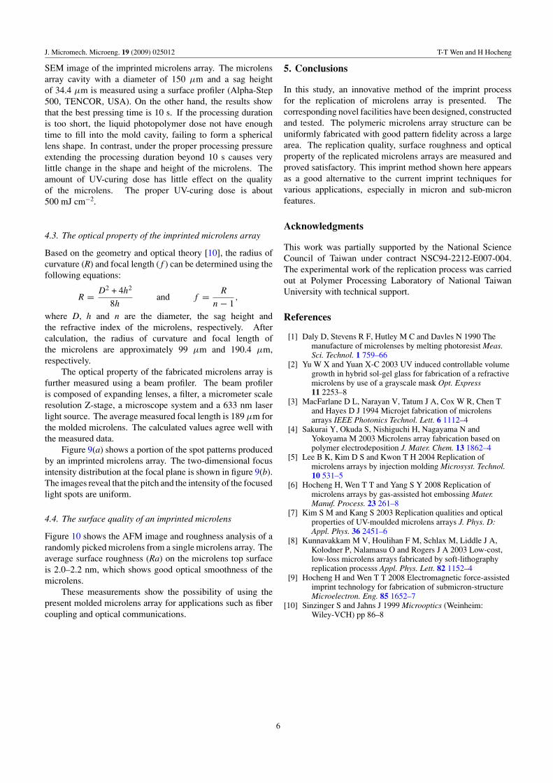
SEM image of the imprinted microlens array. The microlensarray cavity with a diameter of 150 μm and a sag heightof 34.4 μm is measured using a surface profiler (Alpha-Step500, TENCOR, USA). On the other hand, the results showthat the best pressing time is 10 s. If the processing durationis too short, the liquid photopolymer dose not have enoughtime to fill into the mold cavity, failing to form a sphericallens shape. In contrast, under the proper processing pressureextending the processing duration beyond 10 s causes verylittle change in the shape and height of the microlens. Theamount of UV-curing dose has little effect on the qualityof the microlens. The proper UV-curing dose is about500 mJ cm−2.
4.3. The optical property of the imprinted microlens array
Based on the geometry and optical theory [10], the radius ofcurvature (R) and focal length ( f ) can be determined using thefollowing equations:
R = D2 + 4h2
8hand f = R
n − 1,
where D, h and n are the diameter, the sag height andthe refractive index of the microlens, respectively. Aftercalculation, the radius of curvature and focal length ofthe microlens are approximately 99 μm and 190.4 μm,respectively.
The optical property of the fabricated microlens array isfurther measured using a beam profiler. The beam profileris composed of expanding lenses, a filter, a micrometer scaleresolution Z-stage, a microscope system and a 633 nm laserlight source. The average measured focal length is 189 μm forthe molded microlens. The calculated values agree well withthe measured data.
Figure 9(a) shows a portion of the spot patterns producedby an imprinted microlens array. The two-dimensional focusintensity distribution at the focal plane is shown in figure 9(b).The images reveal that the pitch and the intensity of the focusedlight spots are uniform.
4.4. The surface quality of an imprinted microlens
Figure 10 shows the AFM image and roughness analysis of arandomly picked microlens from a single microlens array. Theaverage surface roughness (Ra) on the microlens top surfaceis 2.0–2.2 nm, which shows good optical smoothness of themicrolens.
These measurements show the possibility of using thepresent molded microlens array for applications such as fibercoupling and optical communications.
5. Conclusions
In this study, an innovative method of the imprint processfor the replication of microlens array is presented. Thecorresponding novel facilities have been designed, constructedand tested. The polymeric microlens array structure can beuniformly fabricated with good pattern fidelity across a largearea. The replication quality, surface roughness and opticalproperty of the replicated microlens arrays are measured andproved satisfactory. This imprint method shown here appearsas a good alternative to the current imprint techniques forvarious applications, especially in micron and sub-micronfeatures.
Acknowledgments
This work was partially supported by the National ScienceCouncil of Taiwan under contract NSC94-2212-E007-004.The experimental work of the replication process was carriedout at Polymer Processing Laboratory of National TaiwanUniversity with technical support.
References
[1] Daly D, Stevens R F, Hutley M C and Davles N 1990 Themanufacture of microlenses by melting photoresist Meas.Sci. Technol. 1 759–66
[2] Yu W X and Yuan X-C 2003 UV induced controllable volumegrowth in hybrid sol-gel glass for fabrication of a refractivemicrolens by use of a grayscale mask Opt. Express11 2253–8
[3] MacFarlane D L, Narayan V, Tatum J A, Cox W R, Chen Tand Hayes D J 1994 Microjet fabrication of microlensarrays IEEE Photonics Technol. Lett. 6 1112–4
[4] Sakurai Y, Okuda S, Nishiguchi H, Nagayama N andYokoyama M 2003 Microlens array fabrication based onpolymer electrodeposition J. Mater. Chem. 13 1862–4
[5] Lee B K, Kim D S and Kwon T H 2004 Replication ofmicrolens arrays by injection molding Microsyst. Technol.10 531–5
[6] Hocheng H, Wen T T and Yang S Y 2008 Replication ofmicrolens arrays by gas-assisted hot embossing Mater.Manuf. Process. 23 261–8
[7] Kim S M and Kang S 2003 Replication qualities and opticalproperties of UV-moulded microlens arrays J. Phys. D:Appl. Phys. 36 2451–6
[8] Kunnavakkam M V, Houlihan F M, Schlax M, Liddle J A,Kolodner P, Nalamasu O and Rogers J A 2003 Low-cost,low-loss microlens arrays fabricated by soft-lithographyreplication processs Appl. Phys. Lett. 82 1152–4
[9] Hocheng H and Wen T T 2008 Electromagnetic force-assistedimprint technology for fabrication of submicron-structureMicroelectron. Eng. 85 1652–7
[10] Sinzinger S and Jahns J 1999 Microoptics (Weinheim:Wiley-VCH) pp 86–8
6