innovative device structures and new materials for...
TRANSCRIPT
1
Tahir Ghani
Intel Fellow and Director,
Transistor Technology and Integration,
Intel Corporation
Innovative Device Structures and New
Materials for Scaling Nano-CMOS
Logic Transistors to the Limit
2
Key Messages
• End of traditional dimensional scaling era
• New and rapid innovations in transistor structure and
materials are now key to sustaining Moore’s Law:
Uniaxial strained silicon and HiK + Metal Gate
• Power Limited Era: New Transistor Architectures are
needed to meet the performance improvements while keeping within power budget
• Nanoscale Design Rule Regime: Dimensional scaling does
not mean better transistor performance.
• This is the most exciting time to be doing transistor research
and development
3
Outline� End of Traditional Scaling Era
– Traditional scaling limiters and implications
� Intel’s Response
– Uniaxial Strain (90nm and 65nm Nodes)
– HiK + Metal Gate + Strain (45nm Node)
� Challenges and Solutions Beyond 45nm Node
– Uniaxial Strain: Ultimate limit of silicon mobility enhancement
– Power Limitation: Implications on future transistor structures
– Parasitics Dominated Era: How to address increasing
negative impact of parasitics?
– New Channel Materials: III-V QW FET’s at Vcc~0.5-0.7V
Key requirements for implementing
III-V channels into mainstream?
4
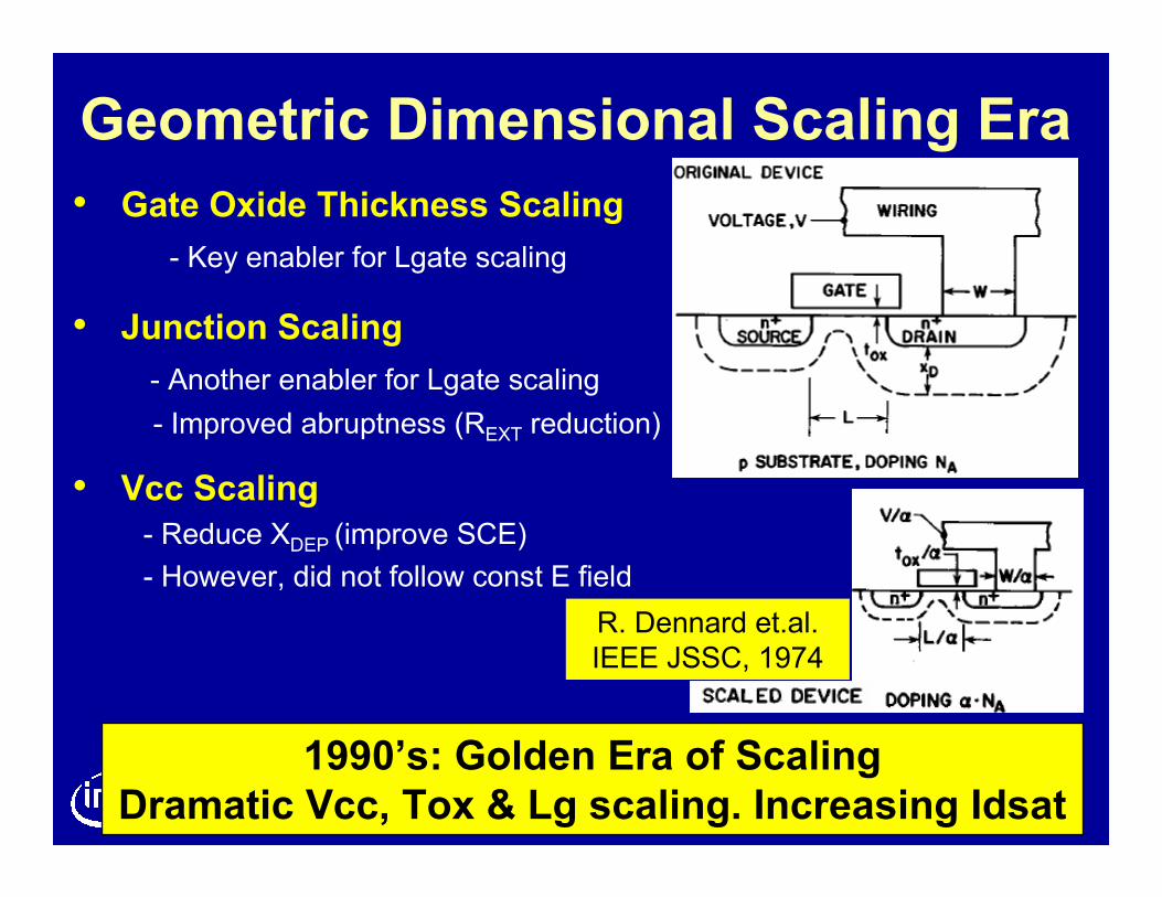
Geometric Dimensional Scaling Era
• Gate Oxide Thickness Scaling
- Key enabler for Lgate scaling
• Junction Scaling
- Another enabler for Lgate scaling
- Improved abruptness (REXT reduction)
• Vcc Scaling
- Reduce XDEP (improve SCE)
- However, did not follow const E field
1990’s: Golden Era of Scaling
Dramatic Vcc, Tox & Lg scaling. Increasing Idsat
R. Dennard et.al.
IEEE JSSC, 1974
5
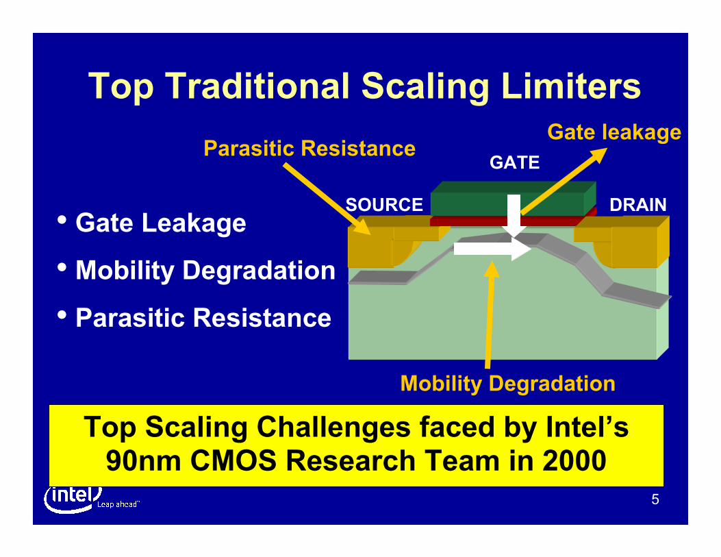
• Gate Leakage
• Mobility Degradation
• Parasitic Resistance
SOURCE DRAIN
GATE
Gate leakage
Mobility Degradation
Top Traditional Scaling Limiters
Top Scaling Challenges faced by Intel’s 90nm CMOS Research Team in 2000
Parasitic Resistance
6
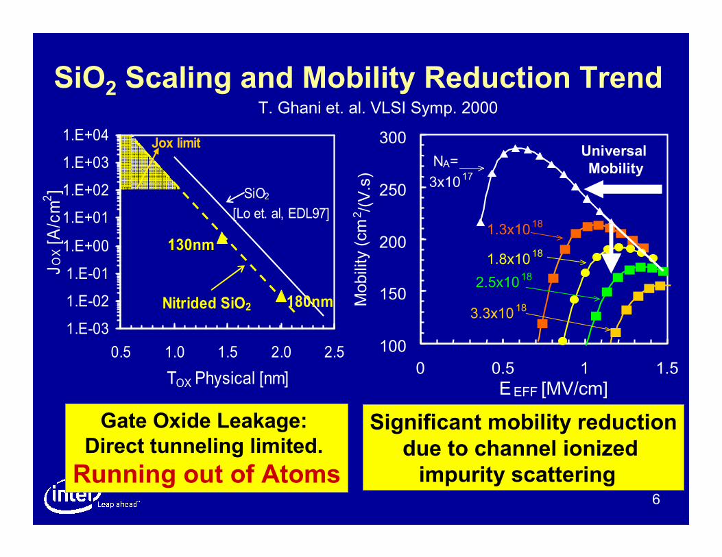
1.E-03
1.E-02
1.E-01
1.E+00
1.E+01
1.E+02
1.E+03
1.E+04
0.5 1.0 1.5 2.0 2.5
TOX Physical [nm]
JOX [A/cm2]
180nmNitrided SiO2
SiO2
[Lo et. al, EDL97]
130nm
Jox limit
T. Ghani et. al. VLSI Symp. 2000
Mobility (cm
2/(V.s)100
150
200
250
300
0 0.5 1 1.5
EEFF [MV/cm]
NA=
3x10¹⁷
1.3x10¹⁸
1.8x10¹⁸
2.5x10¹⁸
3.3x10¹⁸
Universal
Mobility
SiO2 Scaling and Mobility Reduction Trend
Gate Oxide Leakage:
Direct tunneling limited.
Running out of Atoms
Significant mobility reduction
due to channel ionized
impurity scattering
7
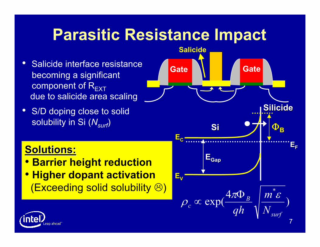
Parasitic Resistance Impact
• Salicide interface resistance
becoming a significant
component of REXTdue to salicide area scaling
• S/D doping close to solid
solubility in Si (Nsurf)
Solutions:Solutions:
• Barrier height reduction • Higher dopant activation(Exceeding solid solubility �)
Gate Gate
Salicide
)4
exp(*
surf
Bc
N
m
qh
επρ
Φ∝
SilicideSilicide
SiSi
EEFF
EEGapGap
EEVV
EECC
ΦΦΦΦΦΦΦΦBB
8
Outline� End of Traditional Scaling Era
– Traditional scaling limiters and implications
� Intel’s Response
– Uniaxial Strain (90nm and 65nm Nodes)
– HiK + Metal Gate + Strain (45nm Node)
� Challenges and Solutions Beyond 45nm Node
– Higher Strain: Ultimate limit of silicon mobility enhancement?
– Power Limitation: Implications on future transistor structures
– Parasitics Dominated Era: How to address increasing
negative impact of parasitics?
– New Channel Materials: III-V QW channels at Vcc~0.5-0.7V
9
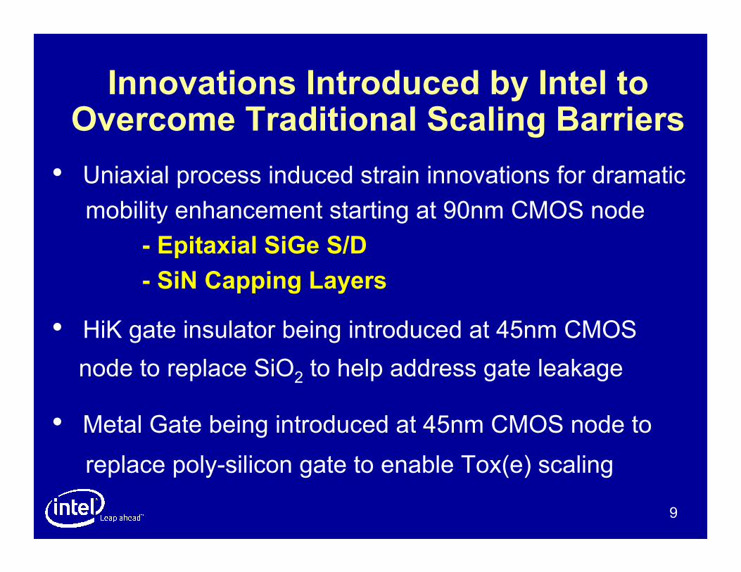
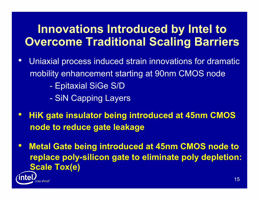
Innovations Introduced by Intel to Overcome Traditional Scaling Barriers
• Uniaxial process induced strain innovations for dramatic
mobility enhancement starting at 90nm CMOS node
- Epitaxial SiGe S/D
- SiN Capping Layers
• HiK gate insulator being introduced at 45nm CMOS
node to replace SiO2 to help address gate leakage
• Metal Gate being introduced at 45nm CMOS node to
replace poly-silicon gate to enable Tox(e) scaling
10
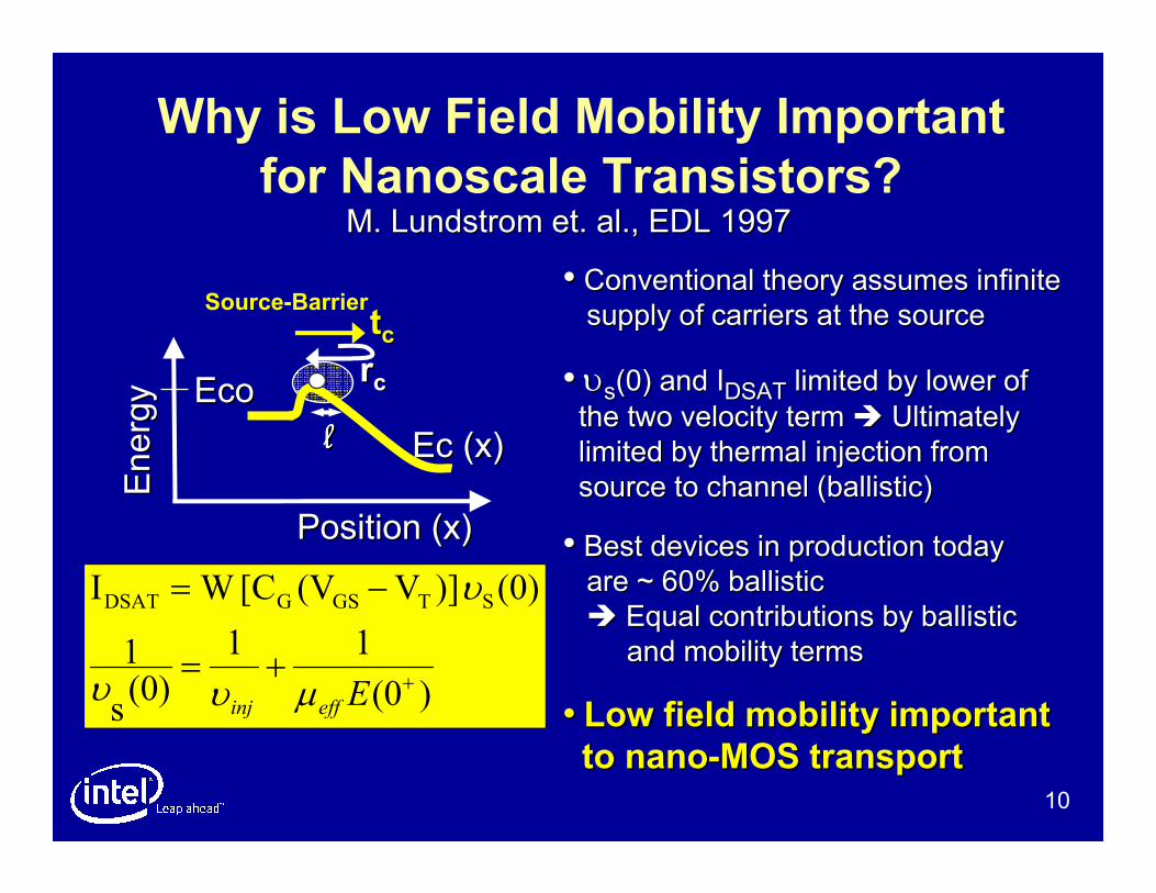
Why is Low Field Mobility Important
for Nanoscale Transistors?M. M. LundstromLundstrom et. al., EDL 1997 et. al., EDL 1997
•• Conventional theory assumes infinite Conventional theory assumes infinite
supply of carriers at the sourcesupply of carriers at the source
•• υυss(0) and I(0) and IDSATDSAT limited by lower of limited by lower of
the two velocity term the two velocity term �� UUltimately ltimately
limited by thermal injection from limited by thermal injection from
source to channel (ballistic)source to channel (ballistic)
•• Best devices in production todayBest devices in production today
are ~ 60% ballistic are ~ 60% ballistic
�� Equal contributions by ballistic Equal contributions by ballistic
and mobility termsand mobility terms
•• Low field mobility important Low field mobility important
to to nanonano--MOS transport MOS transport
)(0
11
(0)s
1
(0) )]V(V[CW I STGSGDSAT
++=
−=
Eeffinj µυυ
υ
EcEc (x)(x)
EcoEco
Position (x)Position (x)
Energy
Energy
llllllll
Source-Barrierttccrrcc
11
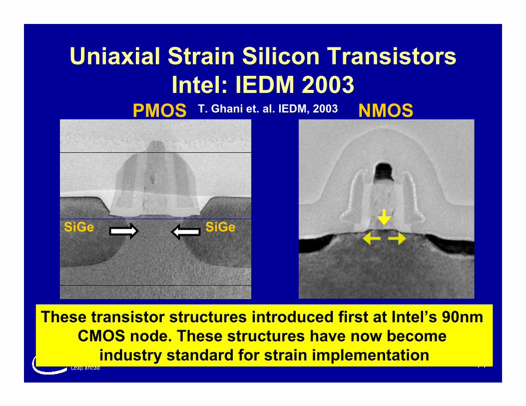
Uniaxial Strain Silicon Transistors
Intel: IEDM 2003PMOS NMOS
SiGeSiGe
These transistor structures introduced first at Intel’s 90nm
CMOS node. These structures have now become
industry standard for strain implementation
T. Ghani et. al. IEDM, 2003
12
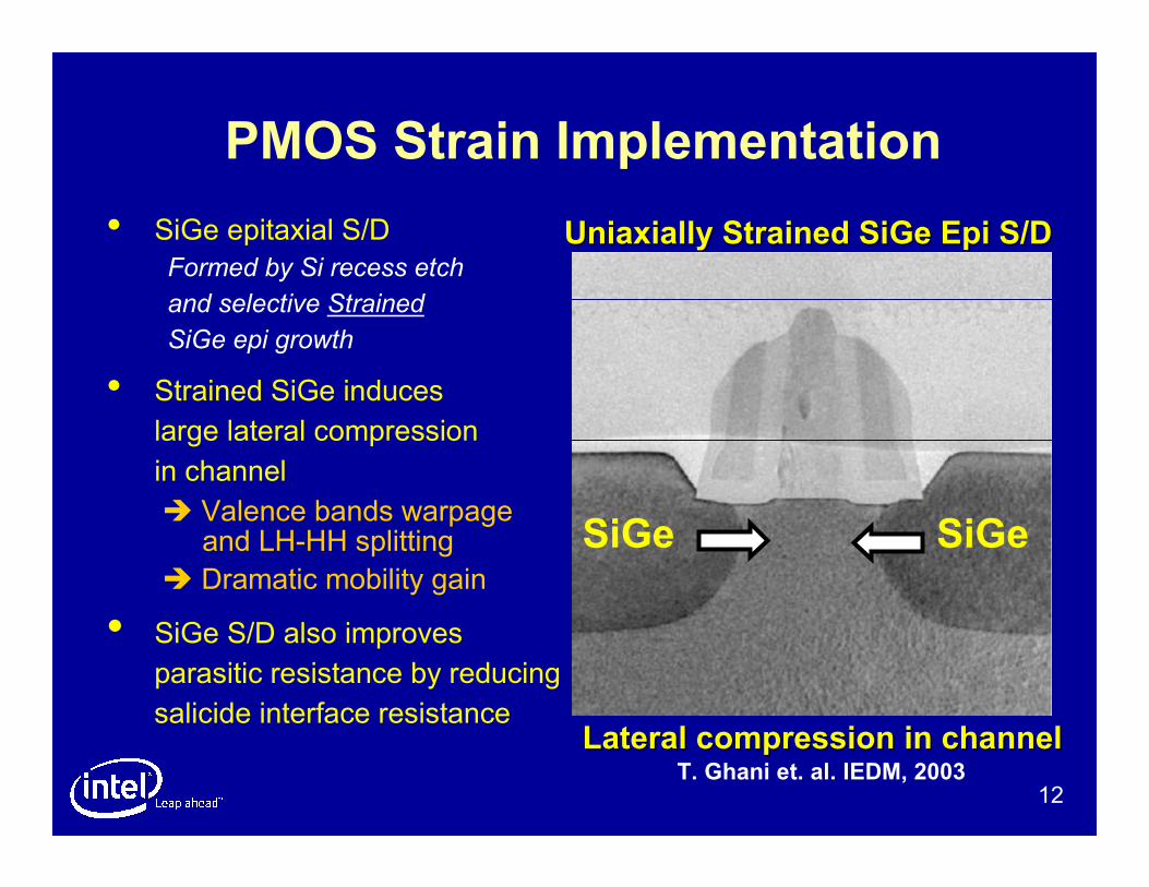
PMOS Strain Implementation
• SiGe epitaxial S/D
Formed by Si recess etch
and selective Strained
SiGe epi growth
• Strained SiGe induces
large lateral compression
in channel
� Valence bands warpageand LH-HH splitting
� Dramatic mobility gain
• SiGe S/D also improves
parasitic resistance by reducing
salicide interface resistanceLateral compression in channelLateral compression in channel
SiGeSiGe
UniaxiallyUniaxially Strained Strained SiGeSiGe EpiEpi S/DS/D
T. Ghani et. al. IEDM, 2003
13
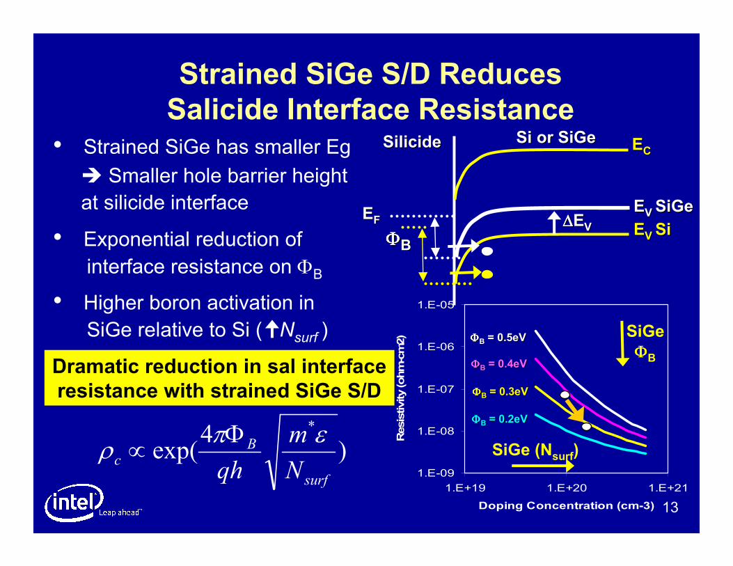
Strained SiGe S/D Reduces
Salicide Interface Resistance • Strained SiGe has smaller Eg
� Smaller hole barrier height
at silicide interface
• Exponential reduction of
interface resistance on ΦB
• Higher boron activation in
SiGe relative to Si ( Nsurf )
Dramatic reduction in sal interface
resistance with strained SiGe S/D
1.E-09
1.E-08
1.E-07
1.E-06
1.E-05
1.E+19 1.E+20 1.E+21
Doping Concentration (cm-3)
Resistivity (ohm-cm2) ΦΦΦΦΦΦΦΦBB = 0.5eV= 0.5eV
ΦΦΦΦΦΦΦΦBB = 0.4eV= 0.4eV
ΦΦΦΦΦΦΦΦBB = 0.3eV= 0.3eV
ΦΦΦΦΦΦΦΦBB = 0.2eV= 0.2eV
SiGe
ΦΦΦΦB
SiGe (Nsurf)
EEFF
ΦΦΦΦΦΦΦΦBB
SilicideSilicide Si or Si or SiGeSiGe EECC
EEV V SiSi
EEV V SiGeSiGe∆∆∆∆∆∆∆∆EEV V
)4
exp(*
surf
Bc
N
m
qh
επρ
Φ∝
14
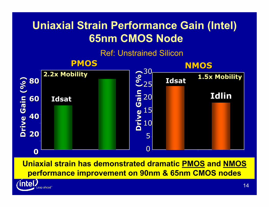
Uniaxial Strain Performance Gain (Intel)
65nm CMOS Node
00
IdlinIdlin
PMOSPMOS
2020
4040
6060
8080
Drive Gain (%)
Drive Gain (%)
00
55
1010
1515
2020
2525
3030
Drive Gain (%)
Drive Gain (%)
IdsatIdsat
IdlinIdlin
NMOSNMOS
IdsatIdsat
Ref: Unstrained Silicon
Uniaxial strain has demonstrated dramatic PMOS and NMOS
performance improvement on 90nm & 65nm CMOS nodes
2.2x Mobility 1.5x Mobility
15
Innovations Introduced by Intel to Overcome Traditional Scaling Barriers
• Uniaxial process induced strain innovations for dramatic
mobility enhancement starting at 90nm CMOS node
- Epitaxial SiGe S/D
- SiN Capping Layers
• HiK gate insulator being introduced at 45nm CMOS
node to reduce gate leakage
• Metal Gate being introduced at 45nm CMOS node to
replace poly-silicon gate to eliminate poly depletion: Scale Tox(e)
16
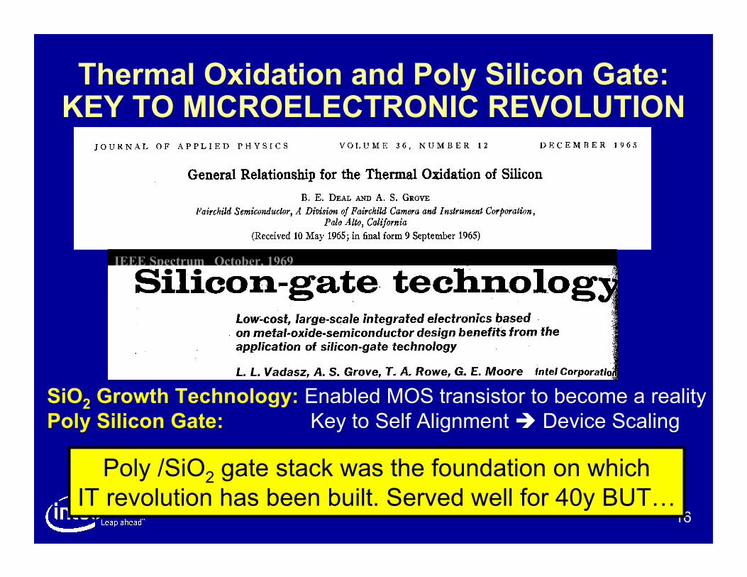
IEEE Spectrum October, 1969
28
Thermal Oxidation and Poly Silicon Gate: KEY TO MICROELECTRONIC REVOLUTION
SiO2 Growth Technology: Enabled MOS transistor to become a reality
Poly Silicon Gate: Key to Self Alignment � Device Scaling
Poly /SiO2 gate stack was the foundation on which
IT revolution has been built. Served well for 40y BUT…
17
1E1E--66
1E1E--44
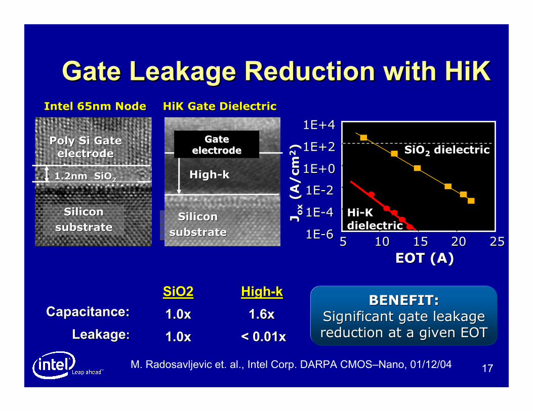
1E1E--22
1E+01E+0
1E+21E+2
1E+41E+4
55 1010 1515 2020 2525
EOT (A)EOT (A)
JJoxox(A/cm
(A/cm
22)) SiOSiO22 dielectricdielectric
HiHi--KK
dielectricdielectric
BENEFIT:BENEFIT:
Significant gate leakageSignificant gate leakage
reduction at a given EOTreduction at a given EOT
SiO2SiO2
1.0x1.0x
1.0x1.0x
HighHigh--kk
1.6x1.6x
< 0.01x< 0.01x
Capacitance:Capacitance:
LeakageLeakage::
Gate Leakage Reduction with Gate Leakage Reduction with HiKHiK
Silicon Silicon
substratesubstrate
Gate Gate
electrodeelectrode
HighHigh--kk
Silicon Silicon
substratesubstrate
1.2nm SiO1.2nm SiO2 2
Poly Si Gate Poly Si Gate
electrodeelectrode
Intel 65nm NodeIntel 65nm Node HiKHiK Gate DielectricGate Dielectric
M. Radosavljevic et. al., Intel Corp. DARPA CMOS–Nano, 01/12/04
18
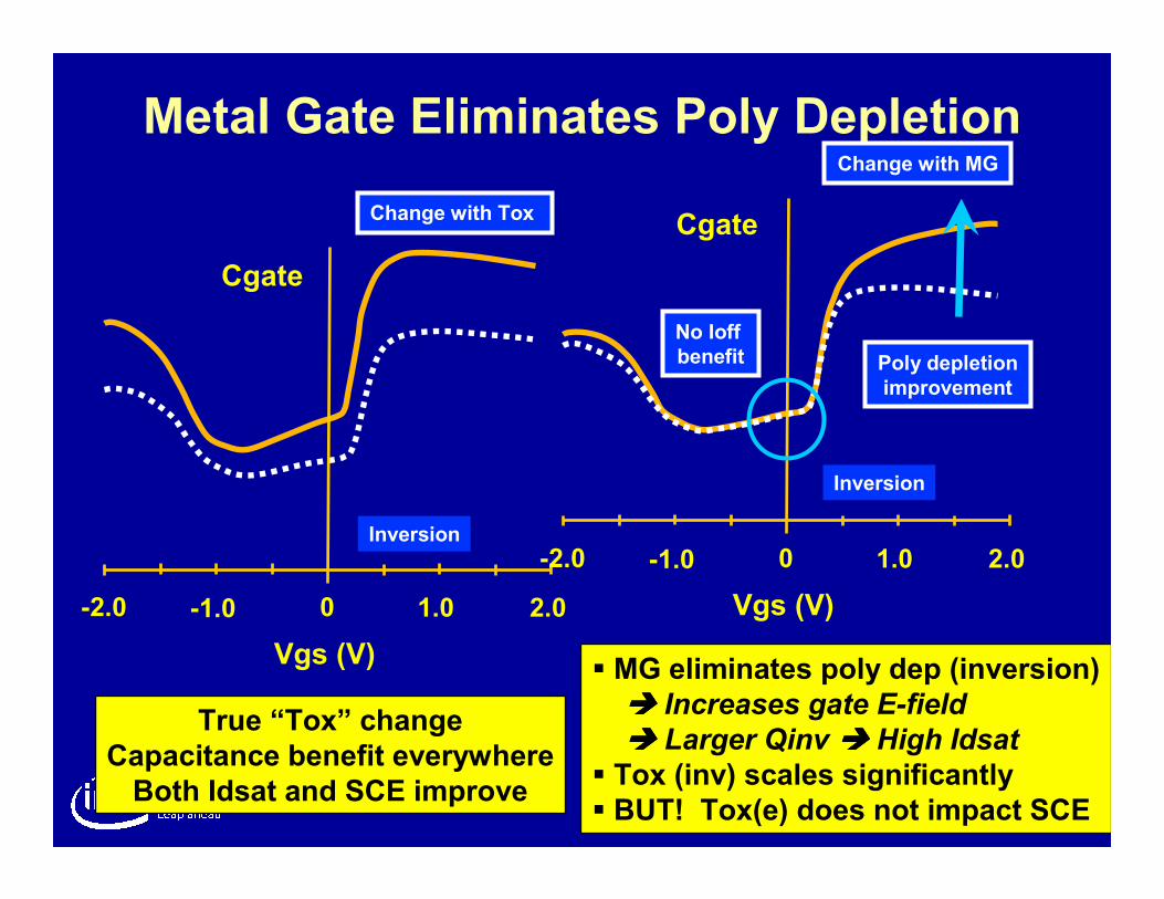
Metal Gate Eliminates Poly Depletion
-2.0 -1.0 0 2.01.0
Vgs (V)
Cgate
Change with Tox
True “Tox” change
Capacitance benefit everywhere
Both Idsat and SCE improve
Inversion
� MG eliminates poly dep (inversion)
���� Increases gate E-field
���� Larger Qinv���� High Idsat
� Tox (inv) scales significantly
� BUT! Tox(e) does not impact SCE
-2.0 -1.0 0 2.01.0
Vgs (V)
Cgate
Change with MG
Inversion
Poly depletion
improvement
No Ioff
benefit
19
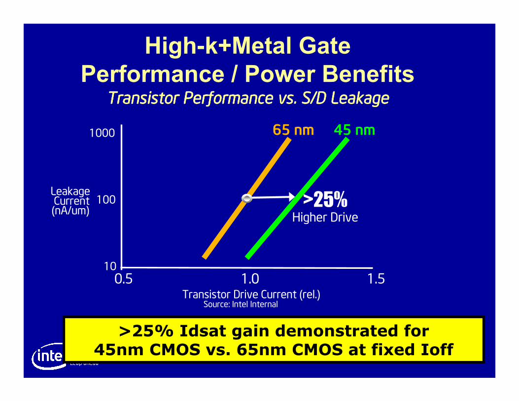
Transistor Drive Current (rel.)
>25%Higher Drive
65 nm 45 nm
10
100
1000
0.5 1.0 1.5
Leakage Current
(nA/um)
Source: Intel Internal
High-k+Metal Gate
Performance / Power BenefitsTransistor Performance vs. S/D LeakageTransistor Performance vs. S/D LeakageTransistor Performance vs. S/D LeakageTransistor Performance vs. S/D Leakage
>25% Idsat gain demonstrated for 45nm CMOS vs. 65nm CMOS at fixed Ioff
20
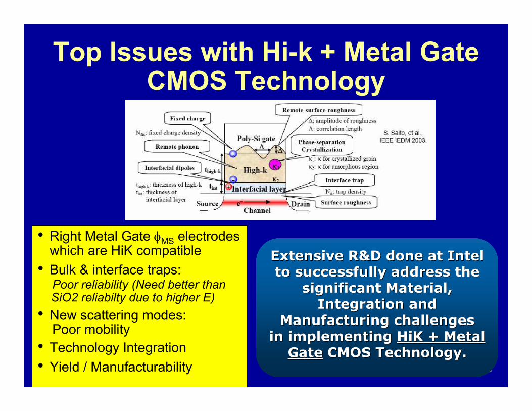
Extensive R&D done at Intel Extensive R&D done at Intel
to successfully address the to successfully address the
significant Material, significant Material,
Integration and Integration and
Manufacturing challenges Manufacturing challenges
in implementing in implementing HiKHiK + Metal + Metal
GateGate CMOS Technology.CMOS Technology.
• Right Metal Gate φMS electrodes which are HiK compatible
• Bulk & interface traps:Poor reliability (Need better thanSiO2 reliabilty due to higher E)
• New scattering modes: Poor mobility
• Technology Integration • Yield / Manufacturability
Top Issues with Hi-k + Metal GateCMOS Technology
21
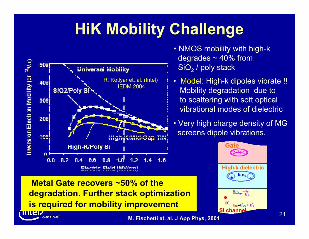
HiK Mobility Challenge
Metal Gate recovers ~50% of the
degradation. Further stack optimization
is required for mobility improvement
• Model: High-k dipoles vibrate !!
Mobility degradation due to
to scattering with soft optical
vibrational modes of dielectric
• Very high charge density of MG
screens dipole vibrations.
• NMOS mobility with high-k
degrades ~ 40% from
SiO2 / poly stack
ELO
Gate
High-k dielectric
Si channel
e-
+ -
-+Eg
E′′′′LOE′′′′g
ETOT=E′′′′LO +E′′′′g
M. Fischetti et. al. J App Phys, 2001
R. Kotlyar et. al. (Intel)
IEDM 2004
22
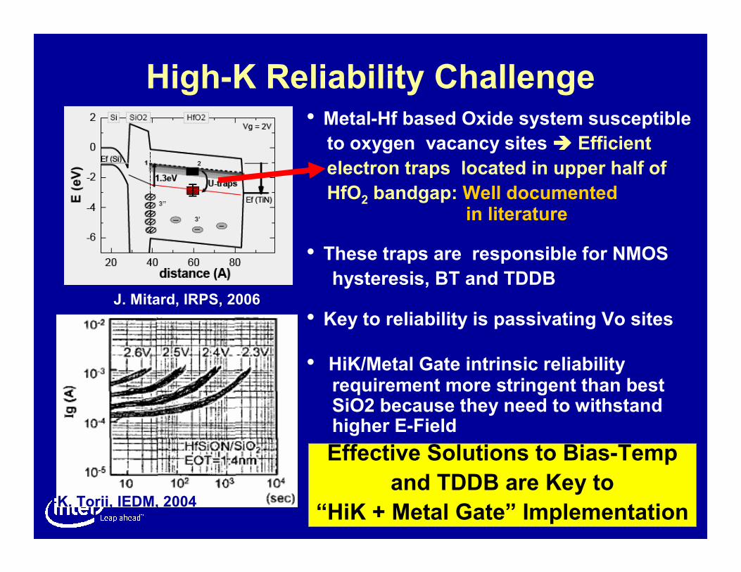
• Metal-Hf based Oxide system susceptible to oxygen vacancy sites ���� Efficient
electron traps located in upper half of
HfO2 bandgap: Well documentedin literature
• These traps are responsible for NMOS hysteresis, BT and TDDB
• Key to reliability is passivating Vo sites
• HiK/Metal Gate intrinsic reliability requirement more stringent than best SiO2 because they need to withstand higher E-Field
K. Torii, IEDM, 2004
J. Mitard, IRPS, 2006
Effective Solutions to Bias-Temp
and TDDB are Key to
“HiK + Metal Gate” Implementation
High-K Reliability Challenge
23
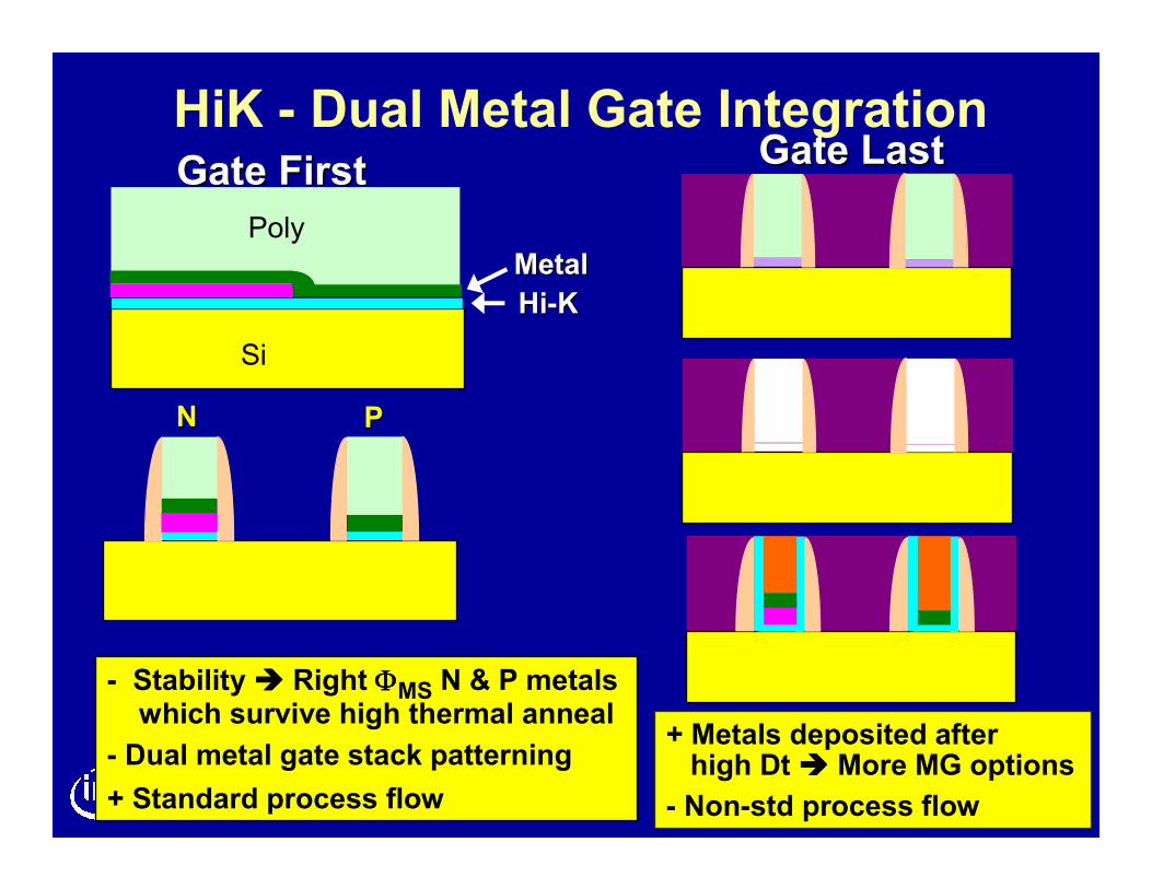
HiK - Dual Metal Gate IntegrationGate FirstGate First
Gate LastGate Last
- Stability ���� Right ΦΦΦΦMS N & P metals which survive high thermal anneal
- Dual metal gate stack patterning
+ Standard process flow
+ Metals deposited after high Dt���� More MG options
- Non-std process flow
Si
Poly
HiHi--KK
MetalMetal
NN PP
24
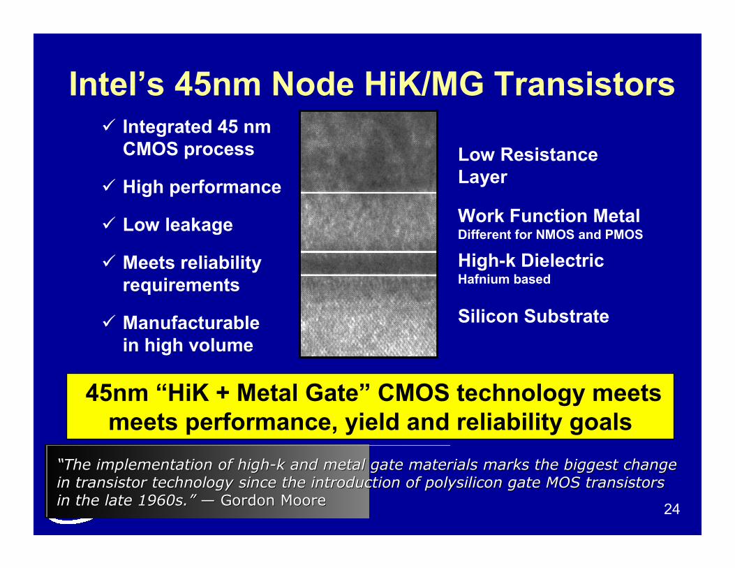
Intel’s 45nm Node HiK/MG Transistors
Low Resistance
Layer
� Integrated 45 nm
CMOS process
� High performance
� Low leakage
� Meets reliability
requirements
� Manufacturable
in high volume
High-k Dielectric Hafnium based
Silicon Substrate
Work Function MetalDifferent for NMOS and PMOS
45nm “HiK + Metal Gate” CMOS technology meets
meets performance, yield and reliability goals
““The implementation of highThe implementation of high--k and metal gate materials marks the biggest change k and metal gate materials marks the biggest change
in transistor technology since the introduction of polysilicon gin transistor technology since the introduction of polysilicon gate MOS transistors ate MOS transistors
in the late 1960s.in the late 1960s.”” —— Gordon MooreGordon Moore
25
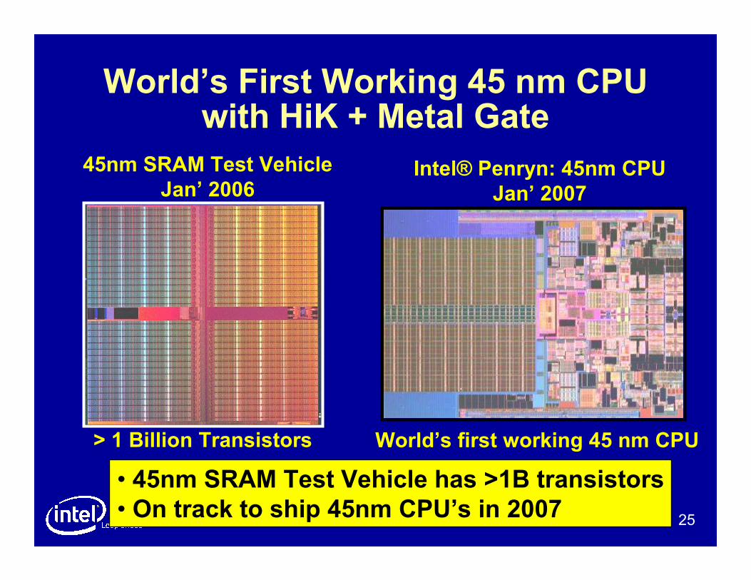
World’s First Working 45 nm CPUwith HiK + Metal Gate
World’s first working 45 nm CPU
Intel® Penryn: 45nm CPU
Jan’ 2007
45nm SRAM Test Vehicle
Jan’ 2006
> 1 Billion Transistors
• 45nm SRAM Test Vehicle has >1B transistors
• On track to ship 45nm CPU’s in 2007

26
Outline� End of Traditional Scaling Era
– Traditional scaling limiters and implications
� Intel’s Response
– Uniaxial Strain (90nm and 65nm Nodes)
– HiK + Metal Gate + Strain (45nm Node)
� Challenges and Solutions Beyond 45nm Node
– Higher Strain: Ultimate limit of silicon mobility enhancement?
– Power Limitation: Implications on future transistor structures
– Parasitics Dominated Era: How to address increasing
negative impact of parasitics?
– New Channel Materials: III-V QW channels at Vcc~0.5-0.7V
27
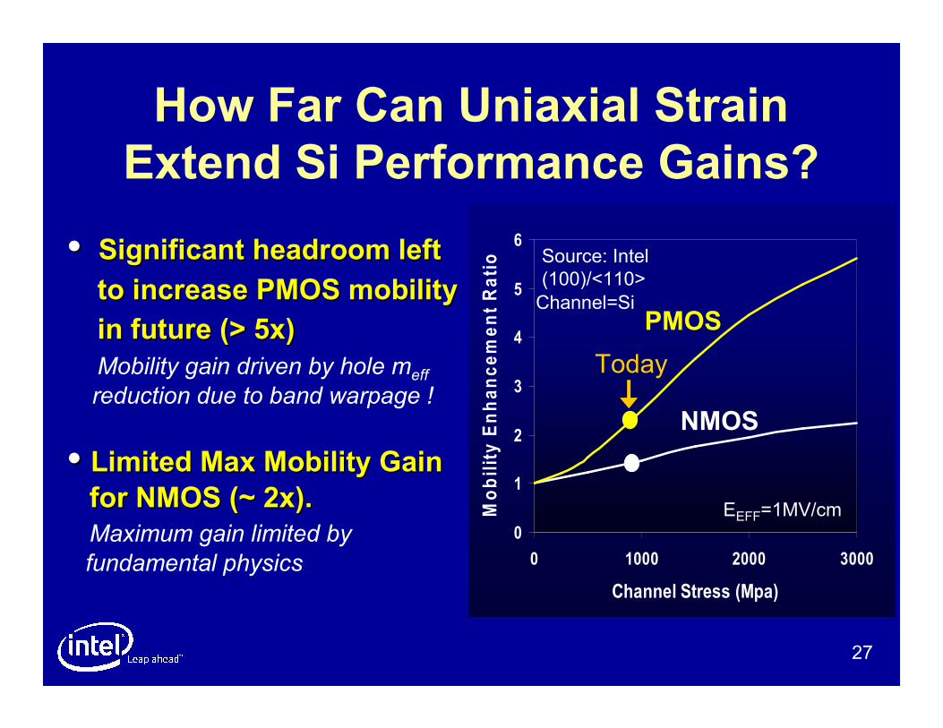
How Far Can Uniaxial Strain
Extend Si Performance Gains?
�� Significant headroomSignificant headroom leftleft
to increase PMOS mobilityto increase PMOS mobility
in future (> 5x) in future (> 5x)
Mobility gain driven by hole meff
reduction due to band warpage !
�� Limited Max Mobility Gain Limited Max Mobility Gain
for NMOS (~ 2x).for NMOS (~ 2x).
Maximum gain limited by
fundamental physics
0
1
2
3
4
5
6
0 1000 2000 3000
Channel Stress (Mpa)
Mobility Enhancement Ratio
PMOS
NMOS
Source: Intel
(100)/<110>
Channel=Si
EEFF=1MV/cm
Today
28
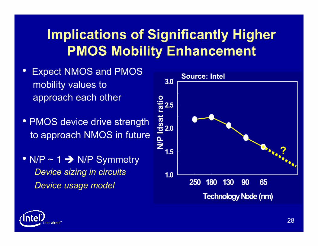
Implications of Significantly Higher
PMOS Mobility Enhancement
• Expect NMOS and PMOSmobility values to
approach each other
• PMOS device drive strength to approach NMOS in future
• N/P ~ 1 � N/P Symmetry
Device sizing in circuits
Device usage model
1.0
1.5
2.0
2.5
3.0
0 1 2 3 4 5 6 7
Technology Node (nm)
N/P Idsat ratio
250 180 130 90 65
Source: Intel
?

29
Outline� End of Traditional Scaling Era
– Traditional scaling limiters and implications
� Intel’s Response
– Uniaxial Strain (90nm and 65nm Nodes)
– HiK + Metal Gate + Strain (45nm Node)
� Challenges and Solutions Beyond 45nm Node
– Higher Strain: Ultimate limit of silicon mobility enhancement?
– Power Limitation: Implications on future transistor structures
– Parasitics Dominated Era: How to address increasing
negative impact of parasitics?
– New Channel Materials: III-V QW channels at Vcc~0.5-0.7V
30
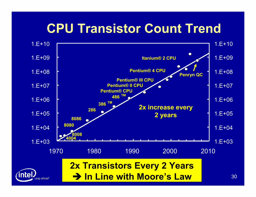
CPU Transistor Count Trend
2x Transistors Every 2 Years
���� In Line with Moore’s Law
1.E+03
1.E+04
1.E+05
1.E+06
1.E+07
1.E+08
1.E+09
1.E+10
1970 1980 1990 2000 2010
1.E+03
1.E+04
1.E+05
1.E+06
1.E+07
1.E+08
1.E+09
1.E+10
4004 8008
8080
8086
286
386 TM
486TM
Pentium® CPU
Pentium® II CPU
Pentium® III CPU
Pentium® 4 CPU
Itanium® 2 CPU
2x increase every
2 years
Penryn QC
31
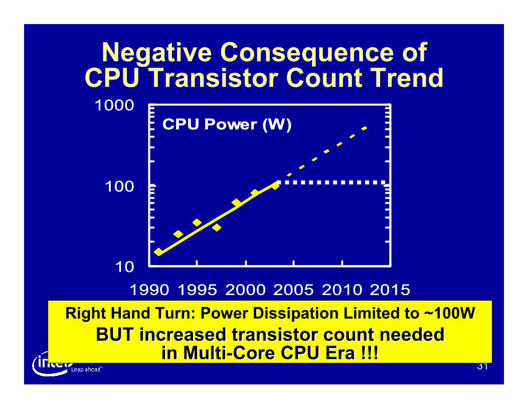
Negative Consequence of CPU Transistor Count Trend
Right Hand Turn: Power Dissipation Limited to ~100W
BUT increased transistor count needed BUT increased transistor count needed in Multiin Multi--Core CPU Era !!!Core CPU Era !!!
CPU Power (W)
10
100
1000
1990 1995 2000 2005 2010 2015
CPU Power (W)
10
100
1000
1990 1995 2000 2005 2010 2015
32
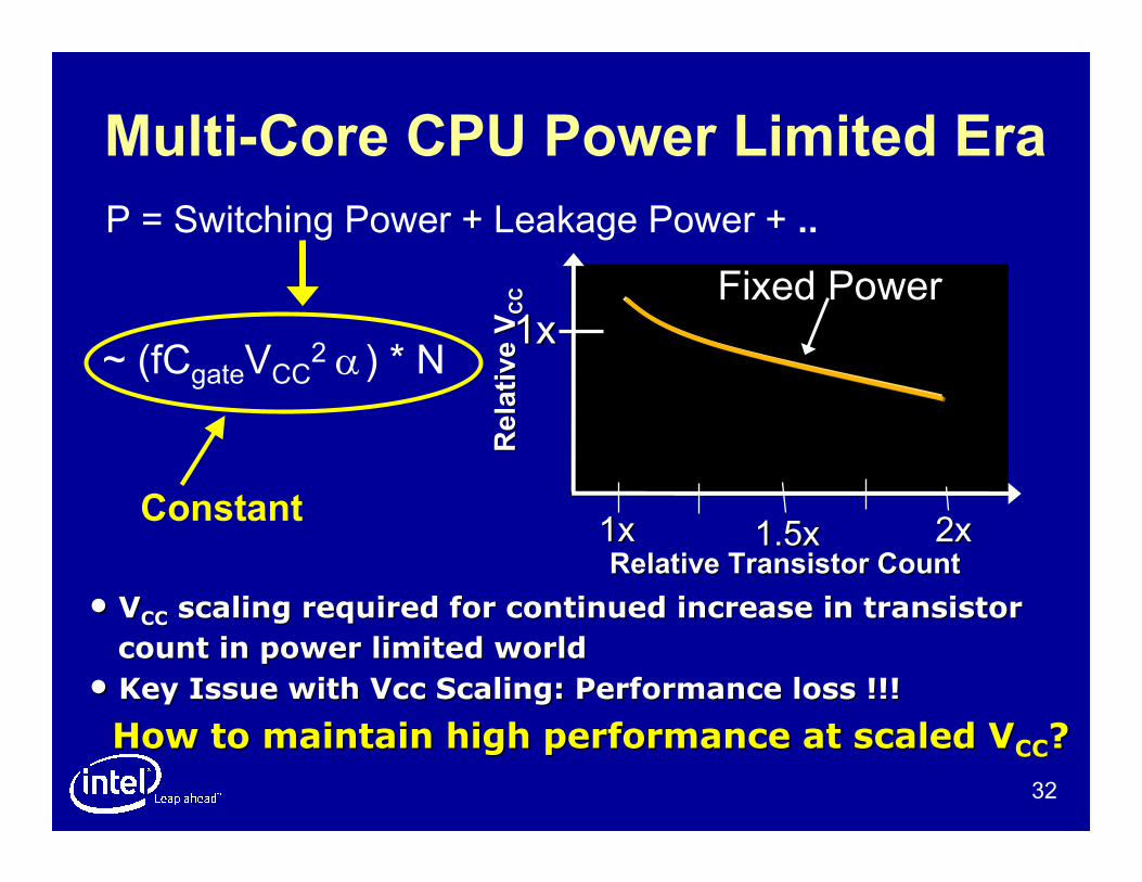
Multi-Core CPU Power Limited Era
P = Switching Power + Leakage Power + ..
~ (fCgateVCC2 ) * N α
Relative V
Relative VCCCC
Relative Transistor CountRelative Transistor Count1x1x 1.5x1.5x 2x2x
Fixed PowerFixed Power1x1x
•• VVCCCC scaling required for continued increase in transistor scaling required for continued increase in transistor
count in power limited worldcount in power limited world
•• Key Issue with Key Issue with VccVcc Scaling: Performance loss !!!Scaling: Performance loss !!!
How to maintain high performance at scaled VHow to maintain high performance at scaled VCCCC??
Constant
33
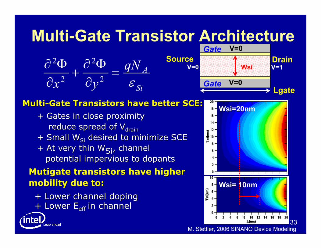
Multi-Gate Transistor ArchitectureV=0
V=0
V=1V=0 WsiDrain
Lgate
Gate
Gate
Source
Wsi=20nm
Wsi= 10nm
Si
AqN
yx ε=
∂
Φ∂+
∂
Φ∂2
2
2
2
M. Stettler, 2006 SINANO Device Modeling
MultiMulti--Gate Transistors have better SCE:Gate Transistors have better SCE:
+ Gates in close proximity+ Gates in close proximity
reduce spread of reduce spread of VVdraindrain
+ Small + Small WWSiSi desired to minimize SCE desired to minimize SCE
+ At very thin + At very thin WWSiSi, channel , channel
potential impervious to potential impervious to dopantsdopants
MutigateMutigate transistors have higher transistors have higher
mobility due to:mobility due to:
+ Lower channel doping + Lower channel doping + Lower + Lower EEeffeff in channel in channel
34
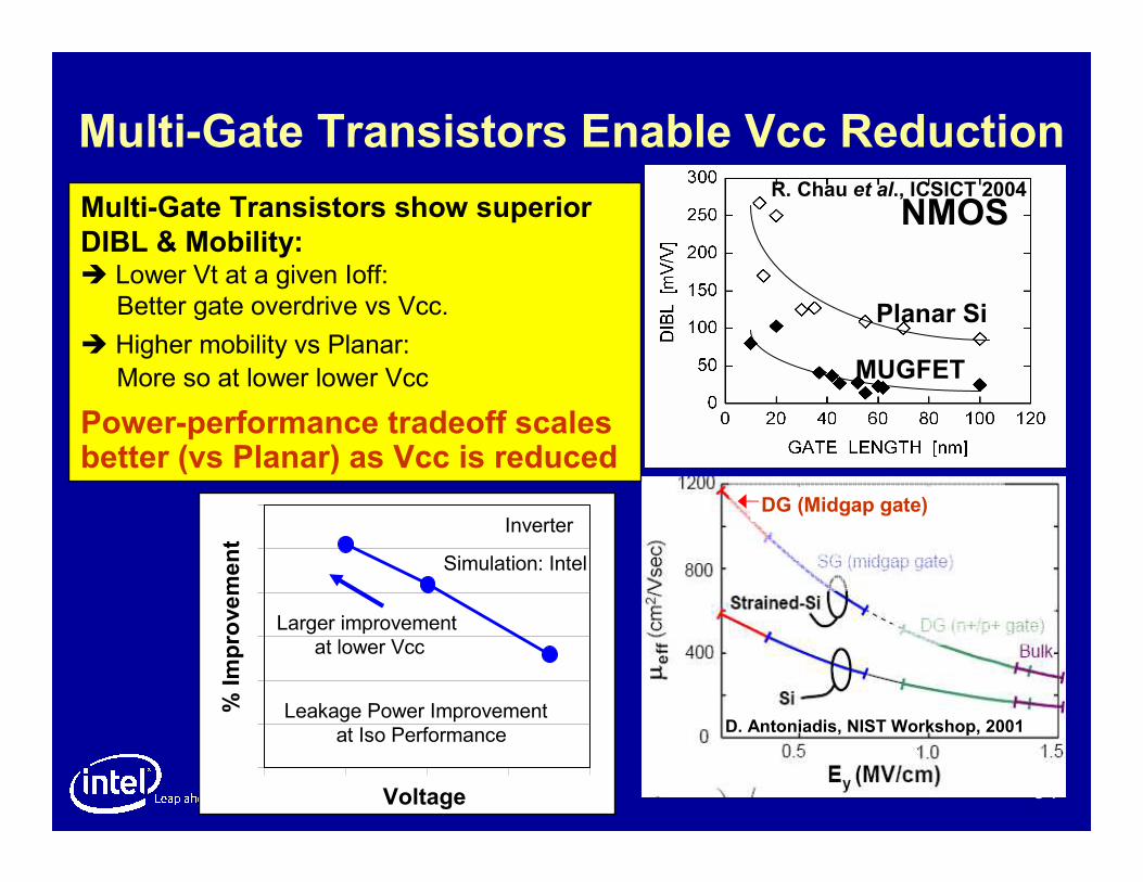
Multi-Gate Transistors Enable Vcc Reduction
MUGFET
Planar Si
NMOSR. Chau et al., ICSICT 2004
DG (Midgap gate)
D. Antoniadis, NIST Workshop, 2001Leakage Power Improvement
at Iso Performance
Inverter
Voltage
% Improvement
Larger improvement
at lower Vcc
Simulation: Intel
Multi-Gate Transistors show superior
DIBL & Mobility:� Lower Vt at a given Ioff:
Better gate overdrive vs Vcc.
� Higher mobility vs Planar:
More so at lower lower Vcc
Power-performance tradeoff scalesbetter (vs Planar) as Vcc is reduced
35
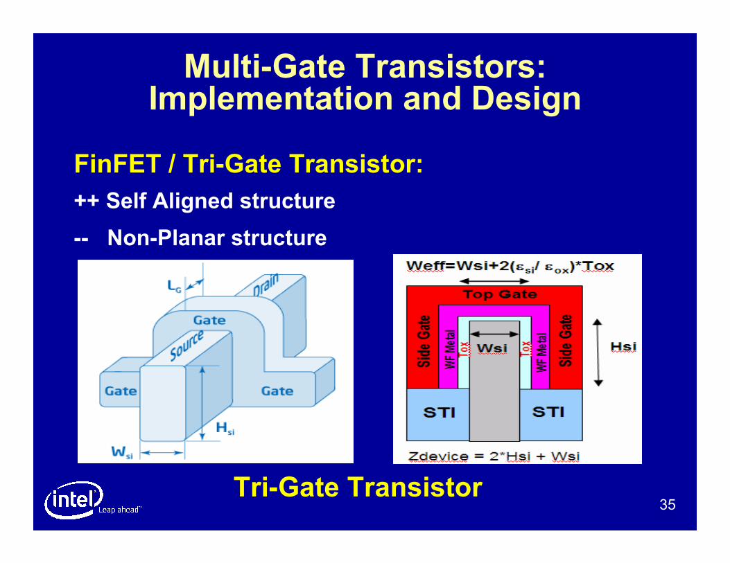
Multi-Gate Transistors: Implementation and Design
FinFET / Tri-Gate Transistor:
++ Self Aligned structure
-- Non-Planar structure
Tri-Gate Transistor
36
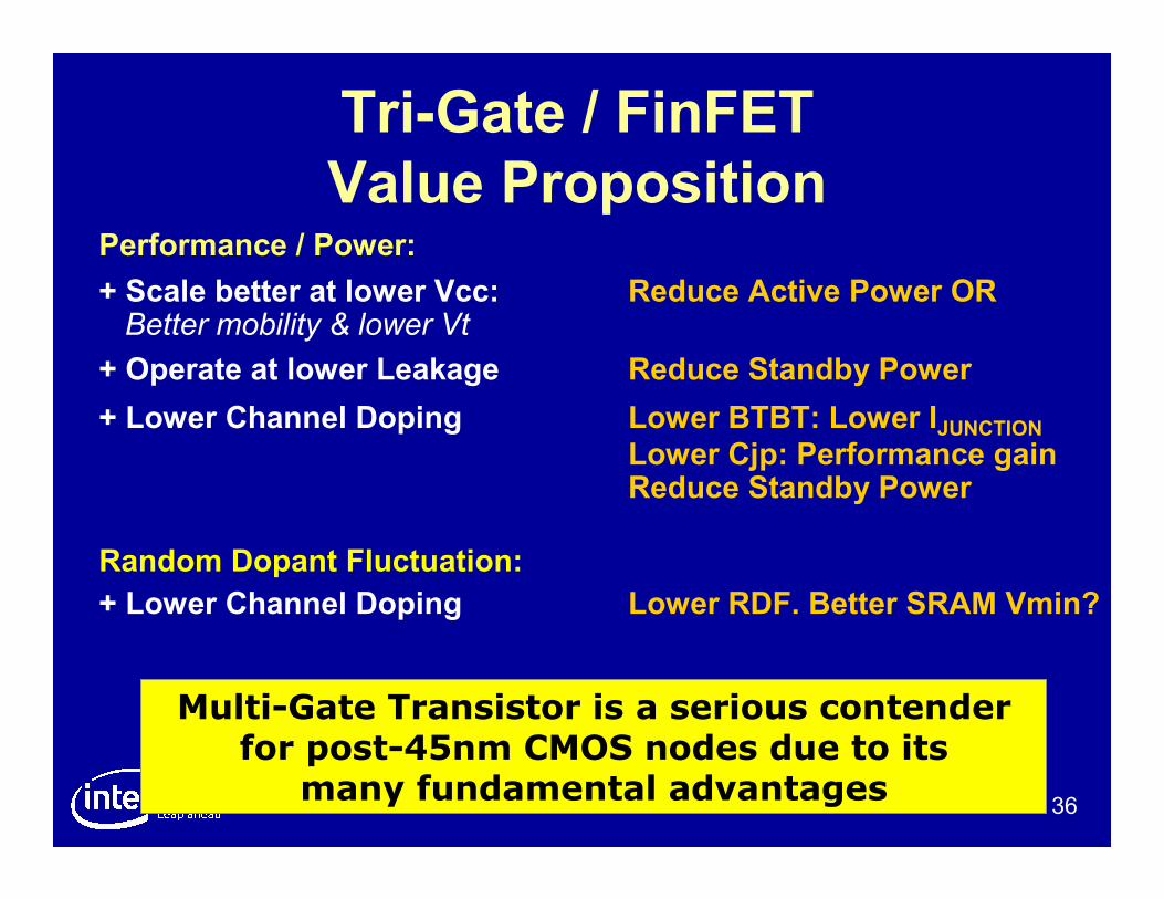
Tri-Gate / FinFET
Value PropositionPerformance / Power:
+ Scale better at lower Vcc: Reduce Active Power ORBetter mobility & lower Vt
+ Operate at lower Leakage Reduce Standby Power
+ Lower Channel Doping Lower BTBT: Lower IJUNCTION Lower Cjp: Performance gainReduce Standby Power
Random Dopant Fluctuation:
+ Lower Channel Doping Lower RDF. Better SRAM Vmin?
Multi-Gate Transistor is a serious contender for post-45nm CMOS nodes due to its
many fundamental advantages
37
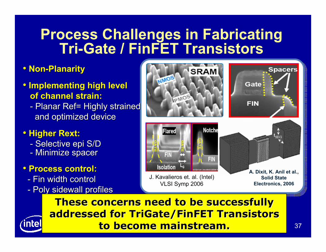
Process Challenges in Fabricating Tri-Gate / FinFET Transistors
J. Kavalieros et. al. (Intel)
VLSI Symp 2006
A. Dixit, K. Anil et al.,
Solid State
Electronics, 2006
•• NonNon--Planarity Planarity
•• Implementing high level Implementing high level
of channel strain:of channel strain:
-- Planar Ref= Highly strainedPlanar Ref= Highly strained
and optimized deviceand optimized device
•• Higher Higher RextRext::
-- Selective Selective epiepi S/DS/D-- Minimize spacerMinimize spacer
•• Process control: Process control:
-- Fin width controlFin width control
-- Poly sidewall profilesPoly sidewall profiles
These concerns need to be successfully These concerns need to be successfully
addressed for addressed for TriGate/FinFETTriGate/FinFET Transistors Transistors
to become mainstream.to become mainstream.

38
Outline� End of Traditional Scaling Era
– Traditional scaling limiters and implications
� Intel’s Response
– Uniaxial Strain (90nm and 65nm Nodes)
– HiK + Metal Gate + Strain (45nm Node)
� Challenges and Solutions Beyond 45nm Node
– Higher Strain: Ultimate limit of silicon mobility enhancement?
– Power Limitation: Implications on future transistor structures
– Parasitics Dominated Era: How to address increasing
negative impact of parasitics?
– New Channel Materials: III-V QW channels at Vcc~0.5-0.7V
39
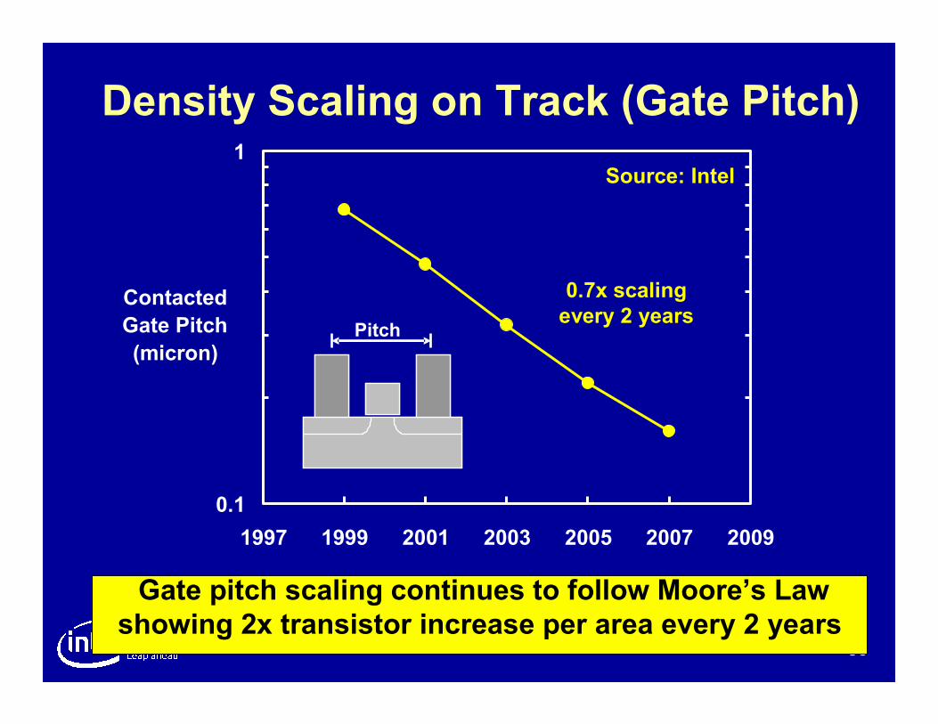
Density Scaling on Track (Gate Pitch)
0.1
1
1997 1999 2001 2003 2005 2007 2009
Contacted
Gate Pitch
(micron)
Source: Intel
Pitch
0.7x scaling
every 2 years
Gate pitch scaling continues to follow Moore’s Law
showing 2x transistor increase per area every 2 years
40
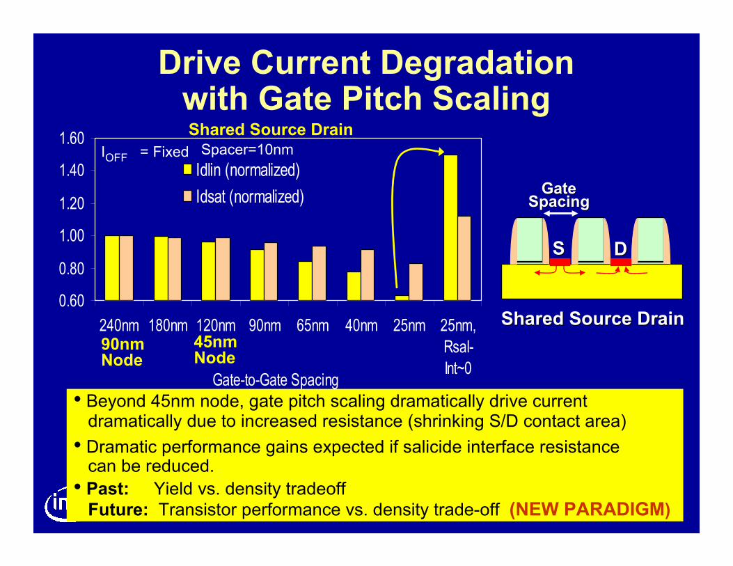
Gate Gate Spacing Spacing
SS DD
Shared Source DrainShared Source Drain
IOFF = Fixed
• Beyond 45nm node, gate pitch scaling dramatically drive currentdramatically due to increased resistance (shrinking S/D contact area)
• Dramatic performance gains expected if salicide interface resistancecan be reduced.
• Past: Yield vs. density tradeoff
Future: Transistor performance vs. density trade-off (NEW PARADIGM)
Drive Current Degradation with Gate Pitch Scaling
0.60
0.80
1.00
1.20
1.40
1.60
240nm 180nm 120nm 90nm 65nm 40nm 25nm 25nm,
Rsal-
Int~0Gate-to-Gate Spacing
Idlin (normalized)
Idsat (normalized)
45nm Node
90nm Node
Shared Source DrainSpacer=10nm
41
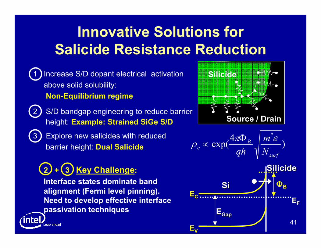
Innovative Solutions for
Salicide Resistance Reduction
1 Increase S/D dopant electrical activation
above solid solubility:
Non-Equilibrium regime
2 S/D bandgap engineering to reduce barrier
height: Example: Strained SiGe S/D
3 Explore new salicides with reduced
barrier height: Dual Salicide
2 + 3 Key Challenge:
Interface states dominate band
alignment (Fermi level pinning).
Need to develop effective interface
passivation techniques
)4
exp(*
surf
Bc
N
m
qh
επρ
Φ∝
Silicide
Source / Drain
SilicideSilicide
SiSi
EEFF
EEGapGap
EEVV
EECC
ΦΦΦΦΦΦΦΦBB
42
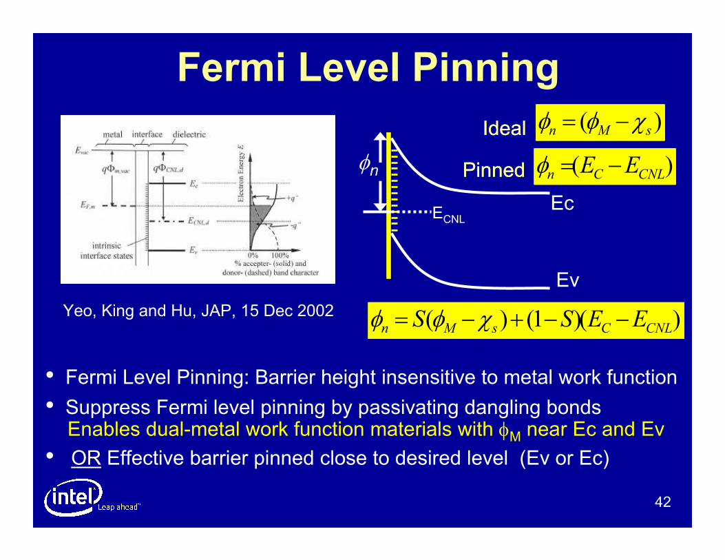
Fermi Level Pinning
Yeo, King and Hu, JAP, 15 Dec 2002 )()1()( CNLCsMn EESS −−+−= χφφ
)( sMn χφφ −=
)( CNLCn EE −=φ
Ideal
Pinned
• Fermi Level Pinning: Barrier height insensitive to metal work function• Suppress Fermi level pinning by passivating dangling bonds Enables dual-metal work function materials with φM near Ec and Ev
• OR Effective barrier pinned close to desired level (Ev or Ec)
)()1()( CNLCsMn EESS −−+−= χφφ
ECNL
φn
)( sMn χφφ −=
)( CNLCn EE −=φ
Ideal
Pinned
Ec
Ev

43
Outline� End of Traditional Scaling Era
– Traditional scaling limiters and implications
� Intel’s Response
– Uniaxial Strain (90nm and 65nm Nodes)
– HiK + Metal Gate + Strain (45nm Node)
� Challenges and Solutions Beyond 45nm Node
– Higher Strain: Ultimate limit of silicon mobility enhancement?
– Power Limitation: Implications on future transistor structures
– Parasitics Dominated Era: How to address increasing
negative impact of parasitics?
– New Channel Materials: III-V QW channels at Vcc~0.5-0.7V
44
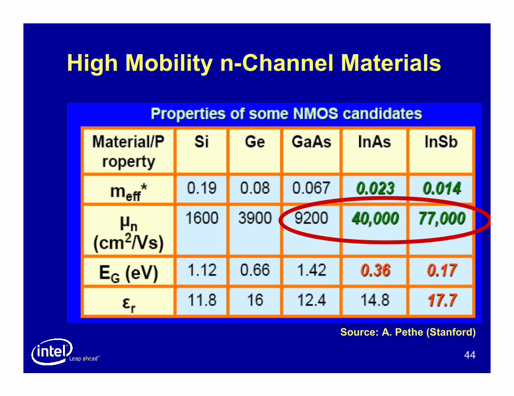
High Mobility n-Channel Materials
Source: A. Pethe (Stanford)
45
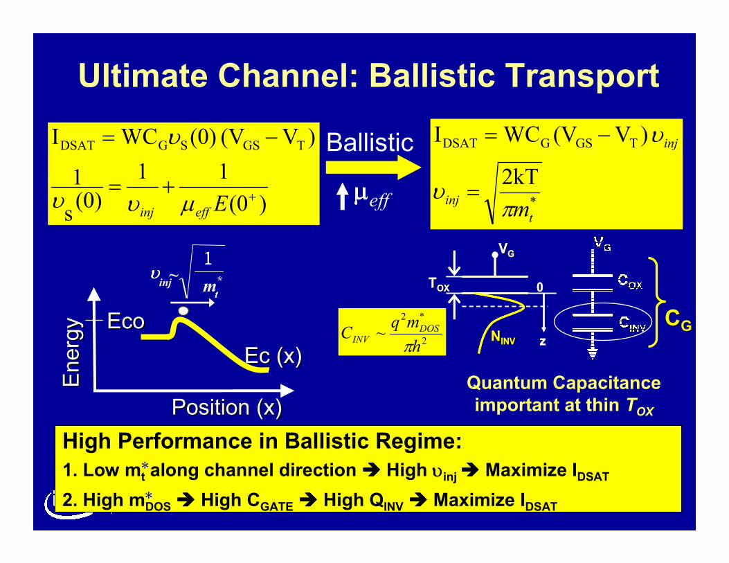
Ultimate Channel: Ballistic Transport
CCGG
Quantum Capacitance
important at thin TOX
)(0
11
(0)s
1
)V(V (0)WCI TGSSGDSAT
++=
−=
Eeffinj µυυ
υ
*
TGSGDSAT
2kT
)V(VWCI
t
inj
inj
mπυ
υ
=
−=
EcEc (x)(x)
EcoEco
Position (x)Position (x)
Energy
Energy
z
0
VVGG
TTOXOX
NNINVINV z
0
VVGG
TTOXOX
NNINVINV
~t
*
1111
minjυυυυ
Ballistic
2
*2
~h
mqC DOSINV
π
High Performance in Ballistic Regime:
1. Low mt along channel direction ���� High υυυυinj���� Maximize IDSAT
2. High mDOS ���� High CGATE ���� High QINV ���� Maximize IDSAT
**
**
µµµµeff
46
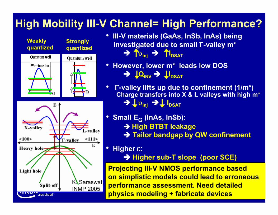
High Mobility III-V Channel= High Performance?
Weakly
quantizedStrongly
quantized
• III-V materials (GaAs, InSb, InAs) being investigated due to small ΓΓΓΓ-valley m*
� υυυυinj � IDSAT
• However, lower m* leads low DOS���� QINV ���� IDSAT
• ΓΓΓΓ-valley lifts up due to confinement (1/m*)Charge transfers into X & L valleys with high m*
���� υυυυinj ���� IDSAT
• Small EG (InAs, InSb):���� High BTBT leakage
���� Tailor bandgap by QW confinement
• Higher ε:ε:ε:ε:���� Higher sub-T slope (poor SCE)
Projecting III-V NMOS performance based
on simplistic models could lead to erroneous
performance assessment. Need detailed
physics modeling + fabricate devices
K. Saraswat,
INMP 2005
47
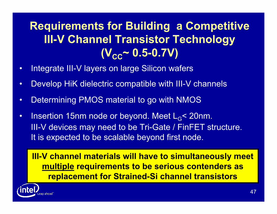
Requirements for Building a Competitive
III-V Channel Transistor Technology
(VCC~ 0.5-0.7V)
• Integrate III-V layers on large Silicon wafers
• Develop HiK dielectric compatible with III-V channels
• Determining PMOS material to go with NMOS
• Insertion 15nm node or beyond. Meet LG< 20nm.
III-V devices may need to be Tri-Gate / FinFET structure.
It is expected to be scalable beyond first node.
III-V channel materials will have to simultaneously meet
multiple requirements to be serious contenders as
replacement for Strained-Si channel transistors
48
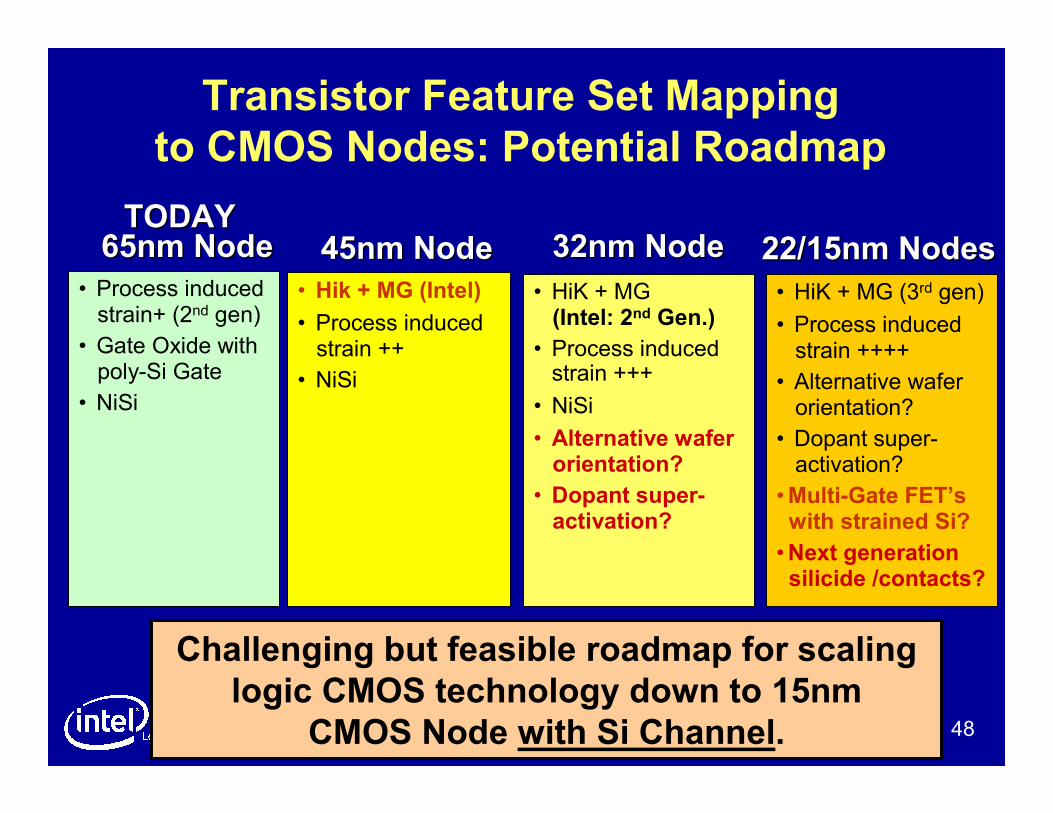
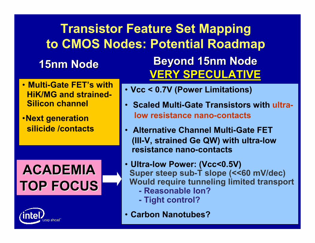
Transistor Feature Set Mapping
to CMOS Nodes: Potential Roadmap
• Process induced strain+ (2nd gen)
• Gate Oxide withpoly-Si Gate
• NiSi
• Hik + MG (Intel)
• Process induced strain ++
• NiSi
• HiK + MG (Intel: 2nd Gen.)
• Process induced strain +++
• NiSi
• Alternative waferorientation?
• Dopant super-activation?
• HiK + MG (3rd gen)
• Process induced strain ++++
• Alternative waferorientation?
• Dopant super-activation?
•Multi-Gate FET’swith strained Si?
•Next generationsilicide /contacts?
65nm Node65nm Node 45nm Node45nm Node 32nm Node32nm Node 22/15nm Nodes22/15nm NodesTODAYTODAY
Challenging but feasible roadmap for scaling
logic CMOS technology down to 15nm
CMOS Node with Si Channel.
49
• Multi-Gate FET’s withHiK/MG and strained-Silicon channel
•Next generation
silicide /contacts
Beyond 15nm NodeBeyond 15nm Node
VERY SPECULATIVEVERY SPECULATIVE15nm Node15nm Node
• Vcc < 0.7V (Power Limitations)
• Scaled Multi-Gate Transistors with ultra-
low resistance nano-contacts
• Alternative Channel Multi-Gate FET
(III-V, strained Ge QW) with ultra-low resistance nano-contacts
• Ultra-low Power: (Vcc<0.5V)Super steep sub-T slope (<<60 mV/dec) Would require tunneling limited transport- Reasonable Ion?- Tight control?
• Carbon Nanotubes?
Transistor Feature Set Mapping
to CMOS Nodes: Potential Roadmap
ACADEMIAACADEMIA
TOP FOCUSTOP FOCUS
50
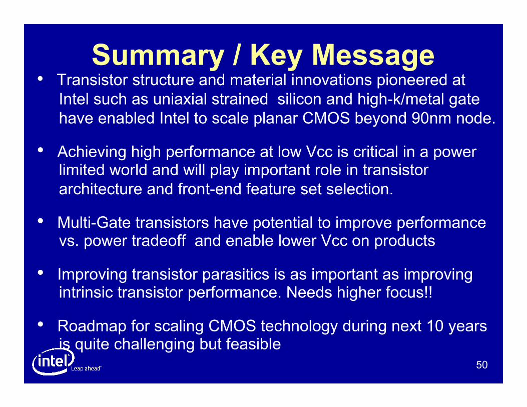
Summary / Key Message• Transistor structure and material innovations pioneered at
Intel such as uniaxial strained silicon and high-k/metal gate
have enabled Intel to scale planar CMOS beyond 90nm node.
• Achieving high performance at low Vcc is critical in a powerlimited world and will play important role in transistor
architecture and front-end feature set selection.
• Multi-Gate transistors have potential to improve performance vs. power tradeoff and enable lower Vcc on products
• Improving transistor parasitics is as important as improving intrinsic transistor performance. Needs higher focus!!
• Roadmap for scaling CMOS technology during next 10 yearsis quite challenging but feasible

51
THANK YOU!