iniŢiere in realizarea practicĂ - · pdf file•schematic drawing in orcad ... fiducial...
TRANSCRIPT

1
INIŢIERE IN REALIZAREA PRACTICĂ A SCHEMELOR ELECTRONICE-PRACTICAL ELECTRONICS-
Web: http://www.cetti.ro
- IRPSE 3-

22
Light-emitting diodes (LEDs) are two-lead devices that are similar to pn-junction diodes, except that they are designed to emit visible or infrared light. When a LED’s anode lead is made more positive in voltage than its cathode lead (by at least 0.6 to 4.1 V), current flows through the device and light is emitted. However, if the polarities are reversed (anode is made more negative than the cathode), the LED will not conduct, and hence it will not emit light. The symbol of a LED is shown in following picture:
LIGHT EMITTING DIODES
Different type of LEDs
Classic "5mm LED" and SMD power LED
Electric drawing symbols for LEDs

33
LED Structure
In conventional package the LED is cylindrical with a hemispherical top that acts as a lens. The leads are relatively thick, to conduct heat away from the component.The cathode leadframehas highly reflective metal (like silver) deposit on the contact surface with semiconductor chip, to form a reflective cavity.

44
Current-Voltage characteristics of the LED
Current-Voltage characteristics of the LED is very important for LED applications. The I-V characteristic of LED is from a typical semiconductor diode.It shows that current increases exponentially as voltage increases. I-V characteristics of different colors of LED are given in the graph, where can be seen different forward voltages according to the color of the LED.
The reverse breakdown voltage of rectifier diodes is usually very high, for instance for 1N4002 this is 200 V and for 1N4007 1000 V.LEDs have usually very low reverse breakdown voltage (Vbr ~5 V)!

55
When a LED is to be connected to a power supply it should be current limitedusing a series resistor to protect it from excessive current flow. The amount of current that flows through an LED must not exceed the value of IF as stated on the LED datasheet.Never connect an LED directly to a battery or power supply as it will be destroyed almost instantly because too much current will pass through and burn it out!From the picture above we can observe that each LED has its own forward voltage drop across the PN junction
In most cases LEDs are operated from a low voltage DC supply, a battery, with a series resistor, RS used to limit the forward current to a safe value from say IF=10 mA for a simple LED indicator.LED Series ResistanceThe series resistor value RS is calculated by simply using Ohm's Law, by knowing the required forward current IF of the LED, the supply voltage VS across the circuit and the expected forward voltage drop of the LED, VF at the required current level.The current limiting resistor is calculated as:
F
FSS I
VVR −=
LED operation

66
Light Emitting Diode Example A blue coloured LED with a forward volt drop of 3.5 volts is to be connected to a 5.0V stabilised DC power supply. Calculate the value of the series resistor required to limit the forward current to less than 10mA. Also calculate the current flowing through the diode if a 100Ω series resistor is used instead of the calculated first.
1. series resistor required at 10mA.
Ω1501010
1.510mA
3.5V5VI
VVR 3F
FSS =
×=−=−= −
2. with a 100Ω series resistor.
mA151001.5
100Ω3.5V5V
RVVI
S
FSF ==−=−=

7

8

9

10
Electric circuit and electronic components mounted on a breadboard
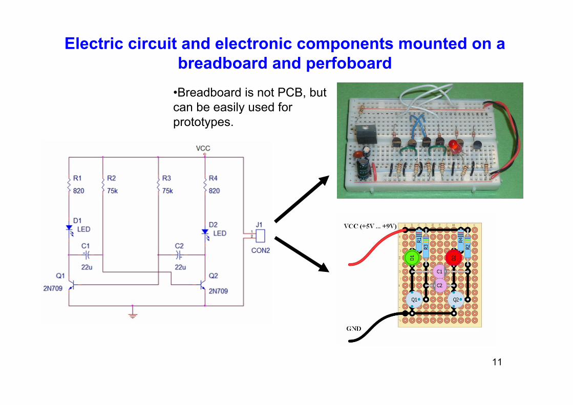
11
Electric circuit and electronic components mounted on a breadboard and perfoboard
•Breadboard is not PCB, but can be easily used for prototypes.
1212
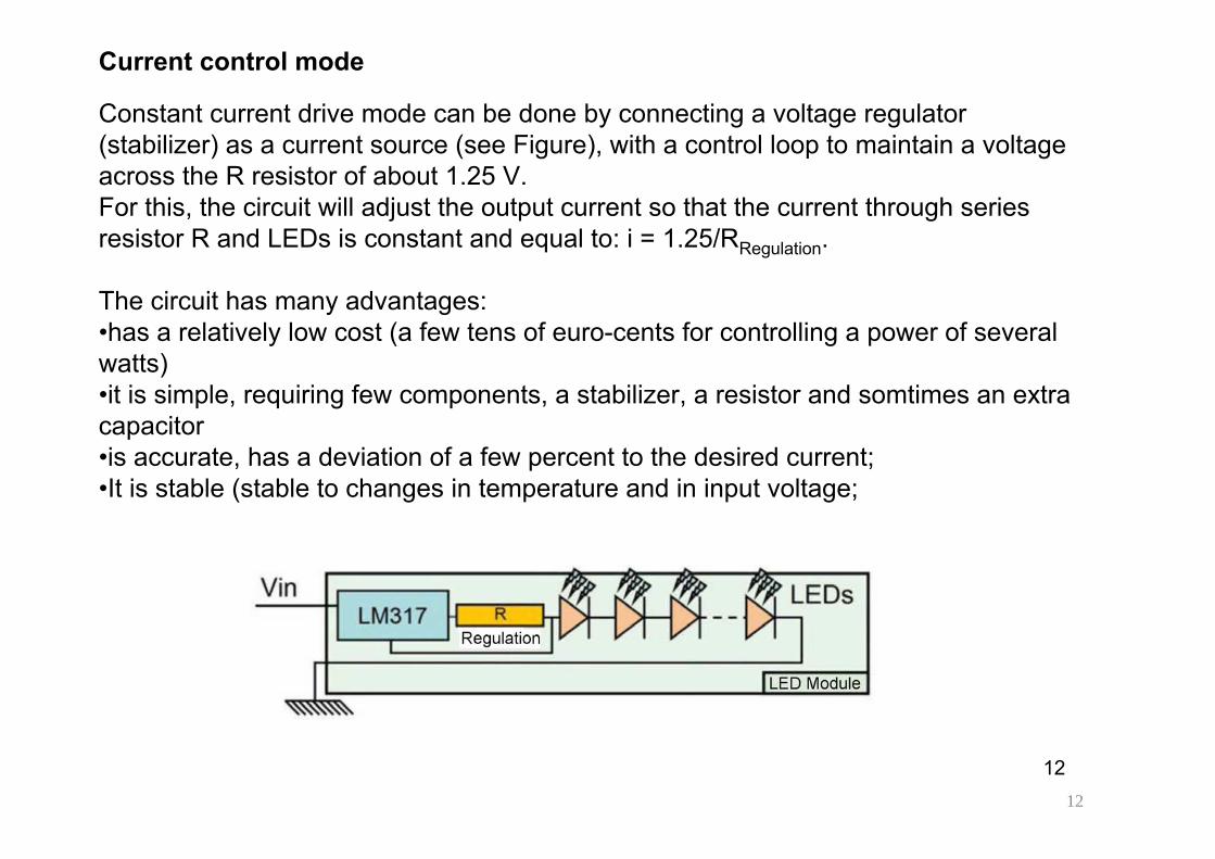
Current control mode
Constant current drive mode can be done by connecting a voltage regulator (stabilizer) as a current source (see Figure), with a control loop to maintain a voltage across the R resistor of about 1.25 V. For this, the circuit will adjust the output current so that the current through series resistor R and LEDs is constant and equal to: i = 1.25/RRegulation.
The circuit has many advantages:•has a relatively low cost (a few tens of euro-cents for controlling a power of several watts)•it is simple, requiring few components, a stabilizer, a resistor and somtimes an extra capacitor•is accurate, has a deviation of a few percent to the desired current;•It is stable (stable to changes in temperature and in input voltage;

1313
The main disadvantage of the circuit is the high power consumption. If the input voltage is too high compared to the voltage across the LED corresponding to selected current, the voltage difference will lead to a higher dissipation in the regulator element, in addition to the resistor. The input voltage can be neither too small, the stabilizing circuit (controller) needs an input voltage higher than the output voltage that ranges between 1.5- 2 V. If we take into account the voltage drop across the resistor, the required voltage at input is at least 3 V higher than the voltage across the LED, for a proper operation of the circuit.
A situation which arises in practice is the supply with an usual voltage of 12V of a series connection with three white LEDs. If the desired mode is current control drive shown in the figure, we compute quickly that at the rated current the LEDs require three 3x3.1V, plus the voltage drop across the resistor 1,25V and at least 1.5-2V for the stabilizer circuit, and we found that the available voltage of 12V is exceeded. There are some stabilizers called "low dropout" LDO having a voltage drop of less than 0.5-0.7 V, which in this case can achieve adequate control of the three white LEDs.
1414
Solid-State Lighting - SSLSSL is an emerging and promising technology that brings benefit over classic incandescent (tungsten) lighting. Some of them are listed below:
1. Energy efficiency: It is energy-efficient; it provides much higher energy conversion efficiency than incandescent lamps which are known to transform only 5% of the consumed energy into visible light, and fluorescent tube lights that are able to change 25% of the energy. 2. Low heat generation: LED lamps are cold devices, producing and radiating less heat into the illuminated regions than bulbs or fluorescent tubes, without any infrared content.3. Can be used to produce light of an intended color without using color filters: LEDsproducing lights of disparate colors are fabricated from different semiconductor materials. Thus, light of each color requires a different LED. 4. Possibility of low voltage, safe battery-driven operation: LED operation does not require high voltages. Low voltages are very safe for users. LED-based lighting may be implemented without the mains supply concerns. 5. Environment friendliness: SSL is pollution-free lighting so that it protects the environment and the climate. It is essentially environment friendly and responsible lighting. It is a “green” light source, free of hazardous substances found in conventional lamp technologies, for example, each fluorescent tube contains 3–5 mg of mercury, which is released into the environment when its glass cover breaks.

1515
LED Packaging (1)
LED packages have evolved from the 5mm circular package (a) to "Piranha" (b) and (c) to LEDs with "thermal pad" (d)
(a)
(b) (c) (d)

1616
The actual packages for high power LEDs have the construction based on ceramic, having on top a protection resin or a silicone material (dome). For the white LEDs, the silicone dome represents a conversion layer, that transforms the blue light into white light.
LED Packaging (2)
A very new package for high power LED is the so called COB (Chip On Board).Different from other package styles, it leaves to user the contacting method to the circuit (PCB).

1717
LEDs thermal managementOne important issue in LED technology is that the emitted light flux is temperature sensitive, as can be seen in the picture.
There are studies to minimize the supplemental costs associated with thermal control in LED lamps.

18
Astable multivibrator circuit with 2 LEDs realized using PCB in THT variant
•Schematic drawing in Orcadsoftware
•Realization of virtual printed circuit (layout) in Orcad

19
Nr. Name Component Value Alternative
1 R1 Resistor 1MΩ, 0603 100kΩ-1MΩ,0603
2 R2 Resistor 100kΩ, 0603
3 R3 Resistor 1kΩ, 0603
4 R4 Resistor 0 Ω, 1210
5 C1, C2 Capacitor 4.7μF, 3216 3.3 - 10μF, 3216
6 D1 LED SMD, 0805
7 U1 IC CD4001 CD4011
Electrolytic capacitor
Fiducial marker
Integrated circuit
Interconnection structure (track)
Solder Pad
Resistor
LED
Astable multivibrator circuit with 2 LEDs and IC in SMT Technology

20
Printed Circuit Boardsand
Assembly and Contacting Technologies for Electronic Components
(continuation)
21
Classification• “Number of layers” criteria: - single layer
- double layer- multi-layer
• “Substrate” criteria: - rigid substrate- flexible substrate- rigid–flex substrate
• “Connection of layers/via” criteria:- with non plated through holes - with plated through holes (PTH)- with special vias- with connection obtained by additive technology

22
Types of PCBs
Single layer PCB (single side )
Double layer PCB with metallized holes (PTH -plated through-hole)
Four layer PCB (multilayer) having two inner planes layers: power and ground.

23
“Special core” PCB Structures“Special core” PCB Structures
Substrat de sticlă Traseu de semnal
Folie inscripţionare Strat de răşină
Applications to circuits with high thermal dissipation (high power LEDs)
Example of “special core” PCB structures, based on glass and Aluminium
Solid Alum inium substrate
Signal track
Resin layer
24
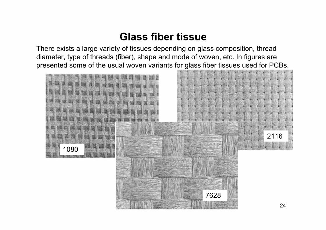
Glass fiber tissue There exists a large variety of tissues depending on glass composition, thread diameter, type of threads (fiber), shape and mode of woven, etc. In figures are presented some of the usual woven variants for glass fiber tissues used for PCBs.
1080
7628
2116
25
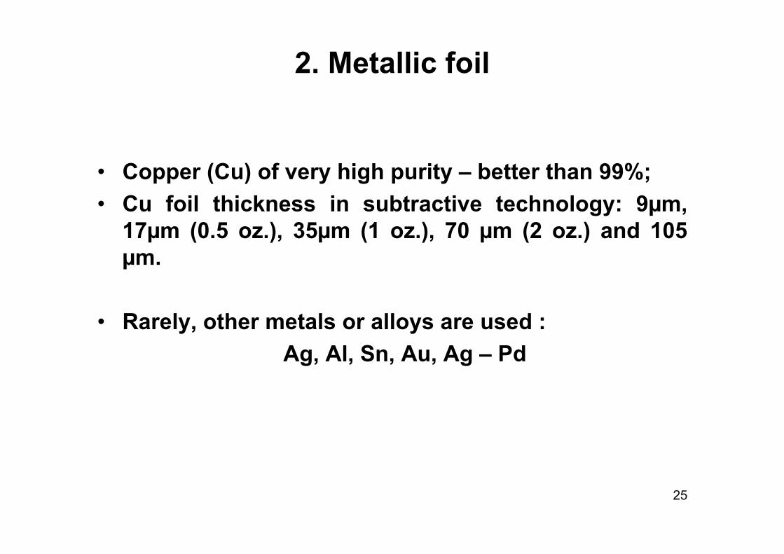
• Copper (Cu) of very high purity – better than 99%;• Cu foil thickness in subtractive technology: 9µm,
17µm (0.5 oz.), 35µm (1 oz.), 70 µm (2 oz.) and 105 µm.
• Rarely, other metals or alloys are used : Ag, Al, Sn, Au, Ag – Pd
2. Metallic foil
26
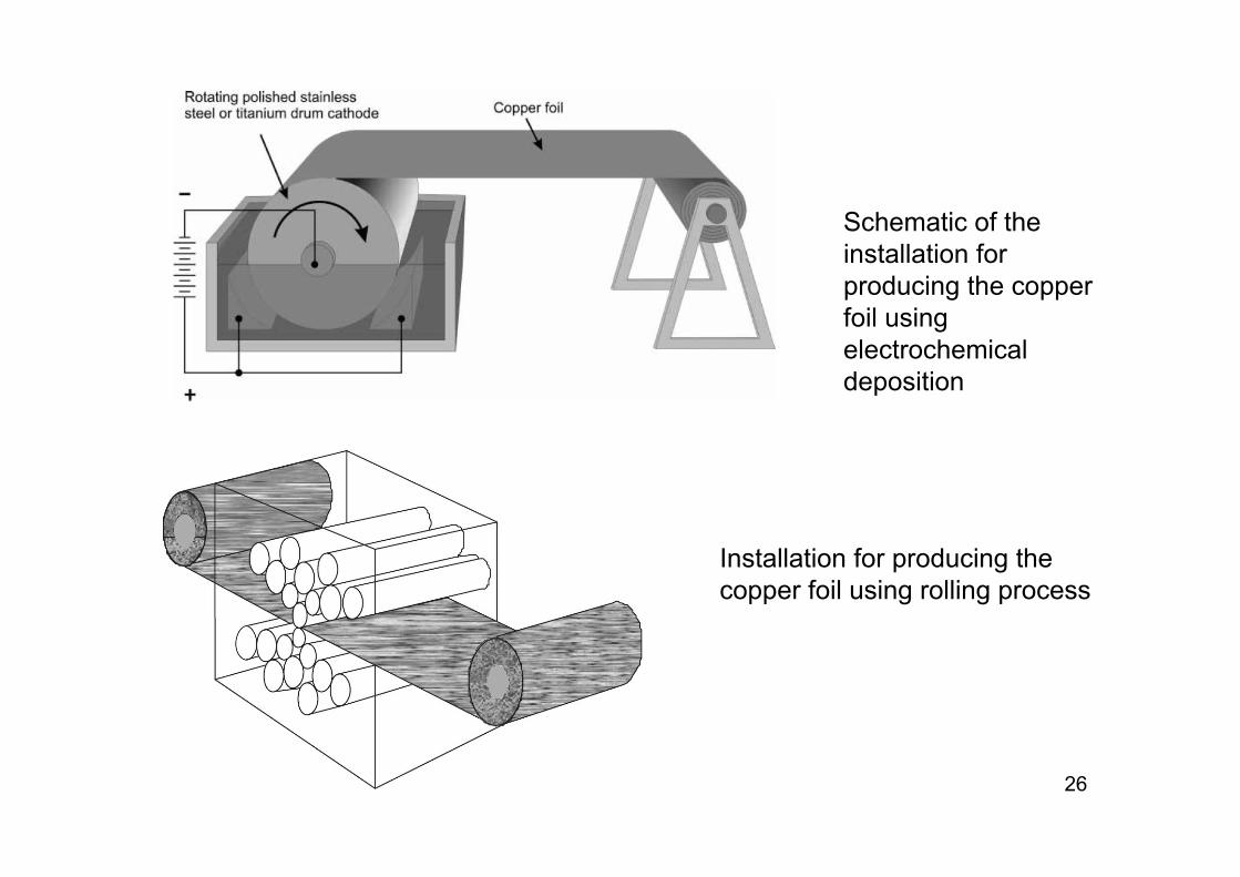
Schematic of the installation for producing the copper foil using electrochemical deposition
Installation for producing the copper foil using rolling process

27
Manufacturing Technologies
Manufacturing Technologies:
1. subtractive;
2. additive;

28
Subtractive Technology Additive Technology

29
Subtractive technologySubtractive technology - mostly used for standard
PCB fabrication on rigid substrate. It is based on“etching” method and “plated through hole” item.
Plated Through Hole (PTH) - the foundation for all electronic packaging and on-board
interconnection of components.

30
1L-PCB (SL-PCB, single-layer PCB) with non-plated through holes (non-PTH)
ManufacturingManufacturing basedbased onon negative negative imageimage
1. Cutting2. Drilling, milling3. Brushing4. Surface preparation5. Transfer of negative image
(silk-screen, offset, photo)
ManufacturingManufacturing basedbased onon positivepositiveimageimage
1. Cutting2. Drilling, milling3. Brushing4. Surface preparation5. Transfer of positive image (silk-
screen, offset)
Two main methods :
Technology of single layer PCBs
31
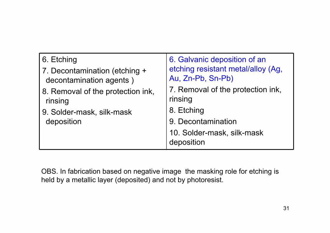
6. Galvanic deposition of an etching resistant metal/alloy (Ag, Au, Zn-Pb, Sn-Pb)7. Removal of the protection ink, rinsing8. Etching9. Decontamination10. Solder-mask, silk-maskdeposition
6. Etching7. Decontamination (etching + decontamination agents )
8. Removal of the protection ink, rinsing
9. Solder-mask, silk-maskdeposition
OBS. In fabrication based on negative image the masking role for etching is held by a metallic layer (deposited) and not by photoresist.
32
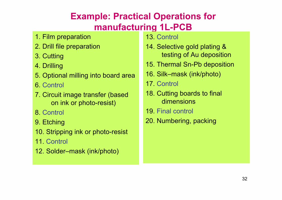
Example: Practical Operations for manufacturing 1L-PCB
1. Film preparation2. Drill file preparation3. Cutting4. Drilling5. Optional milling into board area6. Control7. Circuit image transfer (based
on ink or photo-resist)8. Control9. Etching10. Stripping ink or photo-resist11. Control12. Solder–mask (ink/photo)
13. Control14. Selective gold plating &
testing of Au deposition15. Thermal Sn-Pb deposition16. Silk–mask (ink/photo)17. Control18. Cutting boards to final
dimensions19. Final control20. Numbering, packing

33
Technology of single sided printed circuit boardsBase material (laminate): board covered with copper foil
Positive Mask(photoresist, screen printing)
Etching
Undercutting
Positive Metal Mask (Sn, Sn/Pb…)
Negative Mask(photoresist, screen printing)
"Mushroom" Effect
Mask Removal
Etching
[Metal Mask Removal („orange effect”)
Copper
Photoresist

34
Tehnology of single side printed circuit boards
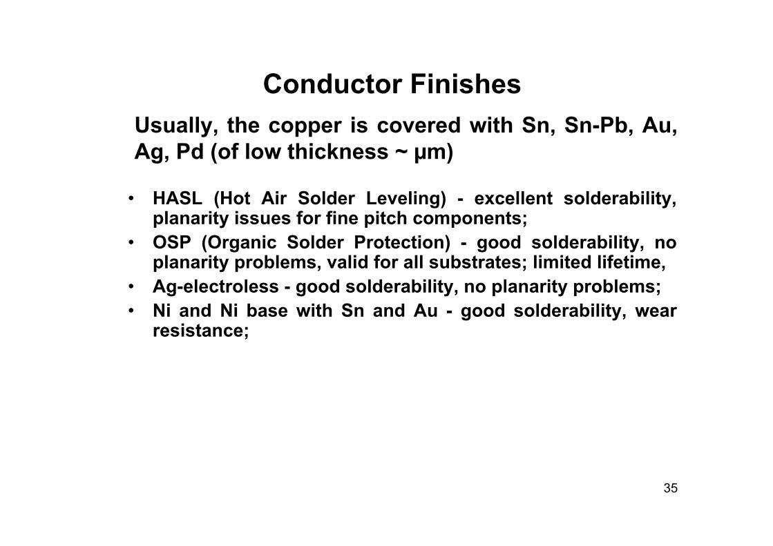
- surface protection
Soldermask
track pad
To improve solderability and for protection : • hot air leveling (plating with eutectic Sn/Pb or SAC alloys )• electroless Ni + Au • immersion Sn• immersion Ag• deposition of organic films (OSP)
35
Conductor Finishes
• HASL (Hot Air Solder Leveling) - excellent solderability, planarity issues for fine pitch components;
• OSP (Organic Solder Protection) - good solderability, no planarity problems, valid for all substrates; limited lifetime,
• Ag-electroless - good solderability, no planarity problems;• Ni and Ni base with Sn and Au - good solderability, wear
resistance;
Usually, the copper is covered with Sn, Sn-Pb, Au, Ag, Pd (of low thickness ~ µm)

36
General manufacturing flow of a 2L-PCB
• Basic cutting 2L PCB laminate;• Drilling and cleaning the holes;• Covering the surface (and the holes) with catalist;• Chemical copper deposition;• Circuit image transfer based on prepared manufacturing
films (ink, photo);• Electro-chemical copper deposition for increasing of copper
thickness;• Electro-chemical deposition of etching protection layer (Sn-
Pb, Zn-Pb, etc.);• Stripping ink, photo-resist;• Etching;• Stripping protection layer;• Drilling holes and milling cut areas;• Applying solder-mask, silk-mask;

37
Technological Flux for PTH double layer printed circuit boards
Double layer laminate
Drilling
Activation; Chemical Cudeposition (electroless)
Photoresist deposition
Photoresist developing
Galvanic Cu deposition (thicker Cu)
Galvanic deposition of an etch resistant layer (Sn-Pb, Sn, Ag, Au)
Photoresist removal
Cu etching
Removal of metallic protective layer
Solder mask printing
Final protective deposition (conductor finish): Sn, OSP, Au-Ni (ENIG), SnPb

38
Solder Mask
Majority of printed circuits are covered with a lacquered deposition we call Solder Mask.Solder Mask is made on a material used for covering the printed circuit board in order to protect it against environmental factors. Solder Mask ensures also a good electrical insulation.
The name of the deposition suggests it's major role: Aid in the soldering process to avoid the solder bridges.

39
Materials used in contacting process
• Alloys used for electric contact - solder alloys;• Flux;• Paste for contact - solder paste;• Auxiliary materials
39

4040
Alloys used for contactingClassification
After melting temperature solder alloys are:
easy melting, having a melting temperature below 450ºC, based on tin (Sn), lead (Pb), cadmium (Cd), bismuth (Bi), zinc (Zn);
hard melting alloys, with melting temperature above 450ºC, based on copper (Cu), silver (Ag), nickel (Ni), manganese (Mn).

4141

42
•Dimensions and particle distribution for solder pastes:•- according Standard ANSI/J-STD-005 and IPC-SF-819
specifications
TypeMax.size
(non larger than)
<0.005% larger than
<1% larger than
>90% between
>10% smaller than
1 180µm 150µm 150-75µm 20µm2 90µm 75µm 75-45µm 20µm3 53µm 45µm 45-25µm 20µm4 45µm 38µm 38-20µm 20µm5 30µm 32µm 25µm 25-15µm 15µm
6 20µm 25µm 15µm 15-5µm 5µm
7 15µm 11µm 11-2µm8 11µm 10µm 8 - 2µm
42

43
Metal content: solder alloy particle content, shape, dimensions, oxygen content.
43

44
•Auxiliary materials used for contacting/soldering
•Solder flux
44

45
Fluxes for solderingPerform two essential functions:•It dissolves and removes impurities from the surface of molten metal before solder alloy extent;•Protect surfaces not to be contaminated the during soldering. Secondary, it ensures the reduction of the surface tension alloy -environment (gas), favoring the alloy spreading.Fluxes must meet several requirements:•To have a melting temperature (TTF) lower than the melting temperature of the alloy (TTA), but shall not completely "burn" at the soldering temperature (TL);•to be in liquid state with a sufficient fluidity at Tt, easy to spread and to get in the interstices;•to dissolve completely and in the time (prior to the melting of the alloy) all impurities, that action must continue as long as the soldering process.
45
46
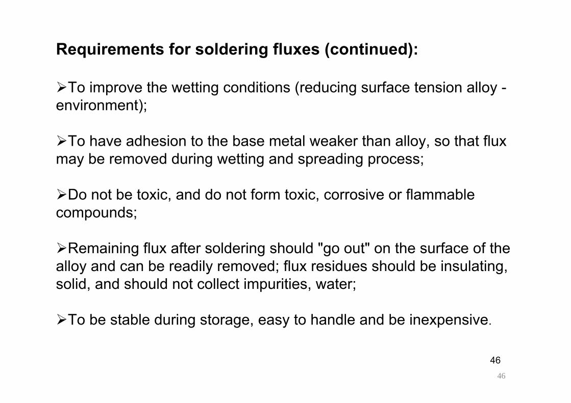
Requirements for soldering fluxes (continued):
To improve the wetting conditions (reducing surface tension alloy -environment);
To have adhesion to the base metal weaker than alloy, so that flux may be removed during wetting and spreading process;
Do not be toxic, and do not form toxic, corrosive or flammable compounds;
Remaining flux after soldering should "go out" on the surface of the alloy and can be readily removed; flux residues should be insulating, solid, and should not collect impurities, water;
To be stable during storage, easy to handle and be inexpensive.
46

47
Types of solder fluxes
active fluxes (corrosive, acidic or caustic remover), typically of inorganic acid (hydrochloric acid, ammonium or zinc chloride, etc.), which cleans the surfaces by chemical attack, forming non-adherent compounds, soluble; to be removed immediately after soldering because the corrosive action continues;
mild activated fluxes – low caustic action, clean the surfaces mainly by dissolving impurities and are formed of organic substances (natural resin with with weak organic acids);
non-activated fluxes (non-corrosive acid-free) without etching action, clean surfaces only by dissolving the impurities and areformed of organic substances (natural resins), often with solvents and wetting improving agents.
In electronics large usage have fluxes without acids and activated fluxes. Acid fluxes are used for mechanical parts or thick cables.
47

48
Fluxes for solderingWidely used fluxes in electronics are based on colophony, a natural resin obtained through distillation of resinous substances from pine wood. Colophony (or rosin) is a mixture of abietic acid (C20H30O2, more than 80%) with other acids and esters. Is a solid substance, glassy aspect, translucent, colored from light yellow to dark brown, with reduced mechanical strength, good insulation properties, non-hygroscopic; is insoluble in water but soluble in majority of organic solvents (alcohol, ether, glycerine).
48
Colophony for violinists, used here for soldering, Source: Wikipedia

49
Colophony softens at 70 ° C and is completely liquid at 125ºC. Colophony dissolves oxides; at 150 °C, dissolve very well copperoxides.
At usual soldering temperatures - more than 210ºC, it boils and burn, releasing smoke with characteristic odor, practically non-toxic.Colophony can be used in solid state as non-activated flux, taken on solder iron tip,or as a film - resulting from the deposit of a colophony lacquer.
Colophony for soldering, used in laboratory, from TME
Colophony for industrial use, mainly used as solved in organic solvents